US6084798A - Non-volatile memory structure - Google Patents

Non-volatile memory structure Download PDF

Info

Publication number
US6084798A
US6084798A US09/345,086 US34508699A US6084798A US 6084798 A US6084798 A US 6084798A US 34508699 A US34508699 A US 34508699A US 6084798 A US6084798 A US 6084798A
Authority
US
United States
Prior art keywords
nonvolatile memory
memory device
metal
transistor
column
Prior art date
Legal status (The legal status is an assumption and is not a legal conclusion. Google has not performed a legal analysis and makes no representation as to the accuracy of the status listed.)
Expired - Lifetime
Application number
US09/345,086
Inventor
Jong Seuk Lee
Current Assignee (The listed assignees may be inaccurate. Google has not performed a legal analysis and makes no representation or warranty as to the accuracy of the list.)
Individual
Original Assignee
Individual
Priority date (The priority date is an assumption and is not a legal conclusion. Google has not performed a legal analysis and makes no representation as to the accuracy of the date listed.)
Filing date
Publication date
Application filed by Individual filed Critical Individual
Priority to US09/345,086 priority Critical patent/US6084798A/en
Application granted granted Critical
Publication of US6084798A publication Critical patent/US6084798A/en
Anticipated expiration legal-status Critical
Expired - Lifetime legal-status Critical Current

Links

Images

Classifications

    • GPHYSICS
    • G11INFORMATION STORAGE
    • G11CSTATIC STORES
    • G11C16/00Erasable programmable read-only memories
    • G11C16/02Erasable programmable read-only memories electrically programmable
    • G11C16/04Erasable programmable read-only memories electrically programmable using variable threshold transistors, e.g. FAMOS
    • G11C16/0408Erasable programmable read-only memories electrically programmable using variable threshold transistors, e.g. FAMOS comprising cells containing floating gate transistors
    • G11C16/0416Erasable programmable read-only memories electrically programmable using variable threshold transistors, e.g. FAMOS comprising cells containing floating gate transistors comprising cells containing a single floating gate transistor and no select transistor, e.g. UV EPROM
    • GPHYSICS
    • G11INFORMATION STORAGE
    • G11CSTATIC STORES
    • G11C16/00Erasable programmable read-only memories
    • GPHYSICS
    • G11INFORMATION STORAGE
    • G11CSTATIC STORES
    • G11C16/00Erasable programmable read-only memories
    • G11C16/02Erasable programmable read-only memories electrically programmable
    • G11C16/06Auxiliary circuits, e.g. for writing into memory
    • G11C16/08Address circuits; Decoders; Word-line control circuits
    • HELECTRICITY
    • H10SEMICONDUCTOR DEVICES; ELECTRIC SOLID-STATE DEVICES NOT OTHERWISE PROVIDED FOR
    • H10BELECTRONIC MEMORY DEVICES
    • H10B41/00Electrically erasable-and-programmable ROM [EEPROM] devices comprising floating gates
    • H10B41/10Electrically erasable-and-programmable ROM [EEPROM] devices comprising floating gates characterised by the top-view layout

Definitions

  • the present invention relates generally to nonvolatile memory devices and more specifically to a Flash EEPROM memory design utilizing a novel NOR-gate transistor array architecture.
  • disk drives tend to be bulky and have a number of moving parts. Consequently, they are prone to reliability problems and consume a significant amount of power.
  • PC's and other digital devices such as cameras and PDA's become smaller and smaller, magnetic disk drive storage becomes even more impractical.
  • Flash electrically erasable programmable read-only memory has emerged as a new source of nonvolatile memory storage.
  • Flash EEPROM memory devices typically comprise an array of floating gate transistors for storing data in digital form.
  • FIG. 1 illustrates the cross-section of a typical NMOS floating gate transistor cell 100 used in Flash EEPROM devices.
  • NMOS transistor cell 100 typically comprises a p-type substrate 102 having a drain region 104 and a source region 106. Drain region 104 and source region 106 typically consist of N+ diffusion regions within p-type substrate 102. A channel region 108 in substrate 102 separates drain region 104 from source region 108.
  • Floating gate 110 is separated from substrate 102 by a thin dielectric layer 114, which in most cases, comprises silicon dioxide.
  • a dielectric layer 116 separates floating gate 110 and control gate 112.
  • the entire structure is overlaid by an oxide insulating layer 118, and means are provided for applying a source voltage VS through oxide layer 118 to source region 106, a gate voltage VG to control gate 112, and a drain voltage VD through oxide layer 118 to drain region 104.
  • drain 104 and control gate 112 are raised to voltage potentials above the voltage potential of source 106.
  • drain 104 is raised to a potential VD of about 5 volts and control gate 112 is raised to a potential VG of about 12 volts.
  • Source 106 is typically grounded. As illustrated in FIG. 1, under such conditions, the current generates hot electrons which become trapped in floating gate 110. This electron injection increases the floating gate threshold by about 3 to 5 volts.
  • drain 104 is typically floated, control gate 112 is grounded and a voltage of about 9 to 12 volts is applied to source 106 for a few milliseconds. As a result, the electrons stored on the floating gate 110 will tunnel through dielectric 114 to drain 104.
  • source 106 is typically held at ground potential and a voltage of about 5 volts is applied to control gate 112. A potential of about 1 to 2 volts is applied to drain 104. Under these conditions, an unprogrammed cell (i.e., no electrons on the floating gate) conducts a current of about 25 to 50 microamps. A programmed cell does not conduct.
  • a typical Flash EEPROM array 200 comprises a plurality of transistors 202 arranged in rows and columns.
  • the drains D of each cell 202 in a column are connected to a common bit line 204.
  • the control gates of each cell 202 in each row are connected to a common word line 206.
  • the source lines of all the cells 202 in the entire array are tied to a common source line 208.
  • cells 202 of array 200 may be individually programmed, but all the cells in array 200 are erased simultaneously because the sources of all the cells are tied together. Thus, to re-program any portion of the array, the entire array first must be erased and then re-programmed. If some of the information stored in the array is to remain the same, that information must be saved in memory during the erase process and then re-programmed back into the array. As one skilled in the art can appreciate, a complex control and memory system is needed to program this type of Flash EEPROM array.
  • Flash EEPROM array designs have been developed to overcome some of the problems associated with having to erase an entire memory array before re-programming it.
  • NAND-gate transistor Flash EEPROM designs have been developed to overcome some of the large block erasing problems associated with the NOR-gate designs. See, for example, "An Experimental 4-Mbit CMOS EEPROM with a NAND-Structured Cell,” M. Momodomi, et al., IEEE Journal of Solid-State Circuits, vol. 24, No. 5, October 1989, pp. 1238-1243, and "A High-Density NAND EEPROM with Block-Page Programming for Microcomputer Applications," Y.
  • the present invention provides a novel nonvolatile Flash EEPROM array design which allows for array, block or sector erase capabilities.
  • the relatively simple transistor design layout of the present invention allows small portions of the EEPROM array to be erased without affecting data stored in the remaining portions of the array.
  • adjacent blocks in the array can share transistor control circuitry, thus minimizing the size of the array.
  • the novel nonvolatile Flash EEPROM array comprises a NOR-gate transistor matrix having at least two rows and two columns of transistors. Each transistor has a drain, a source, and a control gate.
  • the drains of each transistor in a column are electrically coupled
  • the control gates of each transistor in a row are electrically coupled
  • the sources of all the transistors in the matrix are electrically coupled.
  • a sector of the nonvolatile Flash EEPROM array preferably comprises 8 rows and 512 columns of transistors in which the drains in each column of the sector are electrically coupled, the control gates in each row of the sector are electrically coupled and all the sources within the sector are electrically coupled.
  • a sector preferably comprises 512 bytes of nonvolatile memory.
  • a block of the nonvolatile Flash EEPROM array preferably comprises a plurality of vertically stacked sectors.
  • the drains of all transistors within a column of the block are electrically coupled with a common bit line. That is, the drains in a column of one sector are electrically coupled to the drains in the corresponding column of adjacent sectors. In this manner, a block comprises a plurality of continuous columns.
  • control gates in each row of the block are electrically coupled.
  • only the sources within each sector are coupled together.
  • the common sources in each sector are not tied to the common sources of other sectors in the block.
  • a block preferably comprises 128 vertically stacked sectors.
  • a block preferably comprises 64 Kbytes of nonvolatile memory.
  • the nonvolatile Flash EEPROM array may comprise a plurality of rows and or columns of blocks, and adjacent blocks can share control circuitry.
  • FIG. 1 is a side cross-sectional view of a typical NMOS floating gate transistor
  • FIG. 2 is a schematic diagram of a prior art Flash EEPROM transistor array configuration
  • FIG. 3 is a schematic diagram of the transistor configuration of one sector of the Flash EEPROM design of the present invention.
  • FIG. 4 is a top plan view of a circuit layout of a portion of the sector shown in FIG. 3;
  • FIG. 5 is a schematic diagram of the transistor configuration of one block of the Flash EEPROM design of the present invention.
  • FIG. 6 is a block diagram of the Flash EEPROM planar array of the present invention.
  • FIG. 7 is a circuit diagram of a local decoder used in the embodiment of the Flash EEPROM planar array illustrated in FIG. 6.
  • the present invention provides a novel nonvolatile Flash EEPROM array design which allows for array, block or sector erase capabilities. Accordingly, a portion (i.e., a block or sector) of the memory array of the present invention can be erased and reprogrammed with new data without affecting the entire array. While the preferred embodiment of the present invention is described herein with reference to a specific number of transistors in a sector and a specific number of sectors in a block, one skilled in the art will appreciate that any number of transistor may make-up a sector, and any number of sectors may make-up a block. Moreover, any number of blocks may be combined to form the entire Flash EEPROM array. Accordingly, the present invention is not limited to the specific embodiments disclosed herein.
  • a sector of Flash EEPROM memory 300 preferably comprises a plurality of MOS NOR-gate transistor cells 302 arranged in rows and columns.
  • sector 300 comprises 8 rows and 512 columns of transistor cells 302.
  • sector 300 is configured to store 512 bytes of data; each column being 8 bits or 1 byte of data.
  • Each transistor cell 302 comprises a drain 304, a source 306, a control gate 308, and a floating gate 310. As illustrated in FIG. 3, drains 304 of each cell 302 in a column are connected via a bit line 312. Similarly, control gates 308 of each cell 302 in a row are connected via a word line 314. Sources 306 of each cell 302 in sector 300 are connected to a single source connection 316.
  • FIG. 4 illustrates the layout of transistor cells 302 of a portion of sector 300.
  • transistor cells 302 in a column may share common source wells 306 and common drain wells 304.
  • transistor cell 302-1 shares a common source well 306 with transistor cell 302-2
  • transistor cell 302-2 shares a common drain well 304 with cell 302-3.
  • transistor cell 302-3 shares a common source well 306 with transistor cell 302-4, and so on. This configuration allows the transistors to be more densely packed in the array, thus, permitting greater storage capacity in an area smaller than other NOR-gate Flash EEPROM devices currently known in the art.
  • bit lines 312 preferably comprise first metal lines 402 connected to drains 304 by metal to N+ diffusion vias 404.
  • bit lines 312 may be controlled by a common bit line driver, column selector, and sense amplifier, thus reducing the analog circuitry overhead necessary for implementing the memory device.
  • Control gates 308 of transistor cells 302 in a row are all connected via word line 314, which, in accordance with a preferred embodiment, is a polysilicon layer 406.
  • polysilicon layer 406 forms the actual control gates 308 of the transistor cells, as well as the connections between the adjacent gates 308.
  • Floating gates 310 of transistor cells 302 also preferably are formed of polysilicon, but are not connected between the individual transistor cells.
  • the polysilicon floating gates 310 typically reside below polysilicon layer 406 but, for clarity, are not illustrated in FIG. 4.
  • sources 306 of each transistor cell 302 in a sector are tied to a common source connection 316.
  • all sources 306 of transistor cells 302 in a common row are coupled together with an N+ diffusion layer/line 408.
  • N+ diffusion layer 408 forms the source wells 306 of each transistor cell 302, as well as connects source wells 306 along a row.
  • N+ diffusion lines 408 preferably are tied together within sector 300.
  • one or more second metal lines 414 run perpendicular to N+ diffusion lines 408 and are connected to N+ diffusion lines 408 with metal to N+ diffusion vias 416. In this manner, second metal lines 414 interconnect all the parallel N+ diffusion lines 408 in sector 300, effectively linking all sources 306 in sector 300 to common source connection 316.
  • second metal lines 414 may reside either at the same fabrication layer or at a different fabrication layer as first metal lines 402. However, in accordance with a preferred embodiment of the present invention, second metal lines 414 reside at the same layer as first metal lines 402.
  • third metal lines 410 preferably run parallel to N+ diffusion lines 408 and connect to second metal lines 414 with metal to metal vias 412. By connecting third metal lines 410 to N+ diffusion lines 408 via second metal lines 414, the overall resistance of N+ diffusion lines 408 are effectively reduced, thus reducing the power requirements of the Flash EEPROM array.
  • third metal lines 410 are located at different layer from first and second metal lines 402, 414.
  • second metal lines 414 may have any suitable spacing in sector 300.
  • first metal lines can be positioned between about every 16 lines 312 or every 32 lines 312, depending on the resistance of the N+ lines between one contact (416) and another contact (416).
  • second metal line 414 may be utilized.
  • third metal lines 410 positioned over about every other row of drains 304, one should appreciate that any number of third metal lines 410 may be used.
  • third metal lines 410 may be positioned directly over and coupled to N+ diffusion lines 408 with metal to N+ diffusion vias. Alternatively, only one third metal line 410 may be utilized. Accordingly, the present invention is not limited to the illustrated embodiment.
  • block 500 preferably comprises a plurality of sectors 300 stacked vertically one on top of the next. All drains 304 of transistor cells 302 in a column of block 500 are connected to a common bit line 312 via first metal lines 402 (see FIG. 4). In this manner, the vertically stacked sectors 300 all share common bit lines 312. Also, just as transistor cells 302 within a column of a sector can share common source 306 and drain 304 wells (see FIG. 4), transistor cells 302 in adjacent sectors 300 within block 500 can also share common source 306 and drain 304 wells. As mentioned previously, this configuration permits the transistors to be more densely packed within the array. Also, by sharing common bit lines between sectors 300, the total number of bit line drivers, sense amplifiers and column selectors are reduced.
  • block 500 preferably comprises 128 stacked sectors 300. Accordingly, each block 500 comprises 1024 word lines 314 (8 per sector), 128 source connections 316 (one for each sector), and 512 bit lines 312. Thus, block 500 can store up to 64 Kbytes of information:
  • Planar array 600 preferably comprises a plurality of blocks 500 aligned in a one or two dimensional configuration. In accordance with the illustrated embodiment, two rows 602 and four columns 604 of blocks 500 are shown.
  • word line decoders 606, source decoders 608, global decoders 610, and bit line decoders 612 are used. As illustrated in FIG. 6, adjacent horizontal blocks 500 share word line decoders 606 and source decoders 608. For example, in row 602-1 of FIG. 6, block 500-1-1 shares word line decoder 606-1-1 with block 500-1-2, and block 500-1-3 shares word line decoder 606-1-2 with block 5-1-4. Similarly, blocks 500-1-2 and 500-1-3 share source decoder 608-1-2. The second row 602-2 of planar array 600 is similarly configured.
  • planar array 600 is configured so that vertically adjacent blocks 500 share bit line drivers, column selectors and sense amplifiers.
  • bit line drivers, column selectors and sense amplifiers have been grouped together as bit line decoders 612. However, one skilled in the art will appreciate that these components may comprise separate circuitry and they need not be group as one component.
  • a controller In reading, writing and erasing planar array 600 or any block 500 or sector 300 therein, a controller (not shown) typically sends control signals to the various decoders 606-612, directing the decoders to apply suitable voltages to the various bit lines 312, word lines 314 and source connections 316 of the transistors cells 302 being read, written to, or erased.
  • the controller sends the appropriate signals to the specific word line decoder(s) 606, source decoder(s) 608, global decoder(s) 610, and bit line decoder(s) 612 which control the particular transistor cells 302 being read.
  • the various decoders 606-612 then control the voltages on the particular word lines 314, bit lines 312, and common source connections 316 connected to the particular transistor cells 302 being read. Similar operations occur for the write and erase processes.
  • a voltage in the range of about 4 to about 7 volts and preferably about 5 volts is applied to control gate 308 of the transistor cell being read via word line 314.
  • source 306 preferably are grounded and the voltage on drain 304 is measured using bit line decoder 612.
  • transistor cell 302 is programmed with a zero (0) if the voltage on drain 304 is in the range of about 0.5 to about 2 volts and preferably about 1 volt.
  • Transistor cell 302 contains a one (1) if no voltage is detected on drain 304.
  • a voltage of about 0.5 to about 2 volts and preferably about 1 volt is applied to drain 304 via bit line 312, and the current flow in transistor cell 302 is detected using bit line decoder 612.
  • An unprogrammed cell typically conducts about 25 to 50 microamps. A programmed cell does not conduct.
  • a voltage in the range of about 4 to about 7 volts and preferably about 5 volts is applied to control gate 308 of the transistor cell being programmed via word line 314.
  • source 306 of the transistor cell preferably is grounded and a voltage in the range of about 5 to about 9 volts and preferably about 6 volts is applied to drain 304. Under these conditions, electrons from the P-substrate of the transistor cell tunnel through an oxide layer to floating gate 310, thus "programming" a zero (0) therein.
  • the erase function preferably is performed on one or more sectors 300 or one or more blocks 500 of EEPROM array 600.
  • all control gates 308 in sector(s) 300 preferably are grounded, all drains 304 are allowed to float, and a voltage in the range of about 8 to about 12 volts and preferably about 9.5 volts is applied to all sources 306 via common source connection 316. Under these conditions, electrons that were placed in floating gates 310 during the programming process tunnel back through the oxide insulating layer and into drains 304.
  • transistor cells 302 within the sector(s) 300 being erased which were initially programmed with a zero (0) are "erased" back to a one (1) state (i.e., no voltage is detected on drain 304 during the read process.
  • each source decoder 608 is configured to control the voltage potentials on each one of the 128 common source connections 316 in block 500.
  • source decoder 608 applies a suitable voltage to or "selects" one or more entire sectors at a time. If source decoder 608 is shared by two or more blocks 500, source decoder 608 preferably is configured to control the sectors in the blocks separately. For example, referring to FIG. 6, source decoder 608-1-2 can select a specific sector 300 in block 500-1-2 and a different sector 300 in block 500-1-3 simultaneously.
  • each bit line decoder 612 is configured to control each one of the 512 bit lines 312 in block 500 separately
  • each word line decoder 606 is configured to control each one of the 1024 word lines 314 in block 500 separately.
  • specific transistor cells 302 within a particular sector can be read or programmed by applying suitable voltages to specific bit lines 312 and word lines 314 within the sector.
  • suitable voltages are applied to the drains 304 and control gates 308 of the particular transistor cells 302 by bit line decoder 612-1 and word line decoder 606-1-1, respectively.
  • word line decoder 606 is electrically coupled to a global decoder 610 and comprises a partial decoder 702 and a plurality of AND-gates 704.
  • Global decoder 610 receives control signals from a controller and generates a plurality of outputs 706 which act as inputs to AND-gates 704.
  • global decoder 610 includes 128 outputs 706, one for each sector 300 in block 500.
  • partial decoder 702 receives control signals from the controller and generates a plurality of outputs 708 (preferably 8) which also act as inputs to AND-gates 704.
  • the combination of input signals from global decoder 610 and partial decoder 702 generates signals which control one or more word lines 314 in block 500 (See FIGS. 3-5).
  • the output of word line decoder 606 is a plurality of word line connections 710 which are configured to electrically couple to word lines 314.
  • word line decoder 606 comprises 1024 word line connections 710; one for each word line 314 in block 500.
  • global decoder 610 For example, for word line decoder 606 to apply a voltage to or "select" the word line WL12 (see FIG. 7), global decoder 610 generates a signal on output 706-2 pursuant to a control signal from the controller. Similarly, partial decoder 702 generates a signal on partial decoder output 708-4.
  • AND-gate 704 combines the two signals and generates a signal on word line connection 710-12 which is coupled to word line WL12. As one skilled in the art will appreciate, a particular AND-gate 704 will not generate an output unless both the global decoder 606 and the partial decoder 702 transmit high voltages to the particular AND-gate.
  • global decoder 606 To select all word lines 314 within a sector, global decoder 606 generates a high voltage signal for the particular sector selected, and all eight partial decoder outputs 708 are sent high. In accordance with this aspect of the invention, the combination of the output(s) from global decoder 606 with the high outputs from partial decoder 702 produces high voltage signals on all word line connection 710 in the selected sector.
  • the controller for the nonvolatile Flash EEPROM array of the present invention includes circuitry configured to receive externally generated control signals and convert the external signals to internal Flash EEPROM control and data signals.
  • the external signals may be particular address and data signals generated by an Address+Data Pin Interface Protocol.
  • the external address and data signals may be multiplexed into one external signal which can be processed by the control circuitry of the EEPROM array.
  • the Flash EEPROM control circuitry may be configured to interface with and support MSDOS, MSDOS Disk Internal Operations, ATA signal protocol, PCMCIA/ATA signal protocol, Compact Flash signal protocol, and any other memory access protocols currently known or developed in the future.
  • MSDOS MSDOS Disk Internal Operations
  • ATA signal protocol PCMCIA/ATA signal protocol
  • Compact Flash signal protocol Compact Flash signal protocol
  • control circuitry may comprise an error control circuit implementing a fault tolerance scheme such as a 1-bit error correcting Hamming Code to support fault tolerance in a multiple bit per transistor coding scheme.
  • a fault tolerance scheme such as a 1-bit error correcting Hamming Code to support fault tolerance in a multiple bit per transistor coding scheme.
  • the Flash EEPROM control circuitry further comprises a cache memory to optimize both read and write operations. For example, to perform a fast read operation, data stored in the flash memory cell can be dumped into the cache memory, and the data subsequently can be read serially from the cache memory. Similarly, to perform a fast write operation, the data to be written to the flash memory cell can be dumped into the cache memory, and the write operation can occur from the cache memory to the flash memory cell.
  • all the Flash EEPROM control circuitry is fabricated into a single IC chip.
  • the single IC chip may include the cache memory device.
  • the nonvolatile Flash EEPROM transistor array of the present invention may be fabricated into the same IC chip as the control circuitry and cache memory.
  • one IC chip will include everything necessary to implement the Flash EEPROM array of the present invention.
  • the present invention comprises a novel EEPROM design configured for implementing nonvolatile memory structures into large arrays which can be used to form hierarchical memory organizations. While the above is a complete description of the preferred embodiments of the invention, various alternatives, modifications, and equivalents may be used. For example, the size of each array, block and/or sector may be altered to achieve specific design considerations. In addition, a different control circuitry design may be utilized to implement the nonvolatile memory array of the present invention. Therefore, the above description should not be taken as limiting the scope of the invention which is defined by the appended claims.

Landscapes

  • Engineering & Computer Science (AREA)
  • Microelectronics & Electronic Packaging (AREA)
  • Semiconductor Memories (AREA)
  • Non-Volatile Memory (AREA)
  • Read Only Memory (AREA)

Abstract

The present invention provides a novel nonvolatile Flash EEPROM array design which allows for array, block or sector erase capabilities. The relatively simple transistor design layout of the present invention allows small portions of the EEPROM array to be erased without affecting data stored in the remaining portion of the array. In addition, given the block structured layout of the Flash EEPROM array, adjacent blocks in the array can share transistor control circuitry, thus minimizing the size of the array. The novel nonvolatile Flash EEPROM array preferably comprises a plurality of blocks which comprise a plurality of sectors of NOR-gate transistors. Each transistor has a drain, a source, and a control gate. Preferably, the drains of each transistor in a column are electrically coupled, the control gates of each transistor in a row are electrically coupled, and the sources of all the transistors in a sector are electrically coupled. A sector of the nonvolatile Flash EEPROM array preferably comprises 8 rows and 512 columns of transistors and a block preferably comprises 128 vertically stacked sectors.

Description

CROSS-REFERENCES TO RELATED APPLICATIONS
This application is a continuation of U.S. application Ser. No. 09/023,019, filed Feb. 11, 1998, now U.S. Pat. No. 5,956,268, which claims the benefit of U.S. Provisional Application No. 60/037,911, filed Feb. 12, 1997, both of which are incorporated herein by reference.
BACKGROUND OF THE INVENTION
The present invention relates generally to nonvolatile memory devices and more specifically to a Flash EEPROM memory design utilizing a novel NOR-gate transistor array architecture.
Most computers currently use magnetic disk drives for data storage. However, disk drives tend to be bulky and have a number of moving parts. Consequently, they are prone to reliability problems and consume a significant amount of power. Moreover, as PC's and other digital devices such as cameras and PDA's become smaller and smaller, magnetic disk drive storage becomes even more impractical.
Recently, Flash electrically erasable programmable read-only memory (EEPROM) has emerged as a new source of nonvolatile memory storage. Flash EEPROM memory devices typically comprise an array of floating gate transistors for storing data in digital form.
FIG. 1 illustrates the cross-section of a typical NMOS floating gate transistor cell 100 used in Flash EEPROM devices. NMOS transistor cell 100 typically comprises a p-type substrate 102 having a drain region 104 and a source region 106. Drain region 104 and source region 106 typically consist of N+ diffusion regions within p-type substrate 102. A channel region 108 in substrate 102 separates drain region 104 from source region 108.
Positioned above substrate 102 and drain and source regions 104, 106 are a floating gate 110 and a control gate 112, both which typically are formed of polysilicon. Floating gate 110 is separated from substrate 102 by a thin dielectric layer 114, which in most cases, comprises silicon dioxide. Similarly, a dielectric layer 116 separates floating gate 110 and control gate 112. The entire structure is overlaid by an oxide insulating layer 118, and means are provided for applying a source voltage VS through oxide layer 118 to source region 106, a gate voltage VG to control gate 112, and a drain voltage VD through oxide layer 118 to drain region 104.
To program Flash EEPROM transistor cell 100, drain 104 and control gate 112 are raised to voltage potentials above the voltage potential of source 106. For example, drain 104 is raised to a potential VD of about 5 volts and control gate 112 is raised to a potential VG of about 12 volts. Source 106 is typically grounded. As illustrated in FIG. 1, under such conditions, the current generates hot electrons which become trapped in floating gate 110. This electron injection increases the floating gate threshold by about 3 to 5 volts.
To erase the Flash EEPROM transistor cell 100, drain 104 is typically floated, control gate 112 is grounded and a voltage of about 9 to 12 volts is applied to source 106 for a few milliseconds. As a result, the electrons stored on the floating gate 110 will tunnel through dielectric 114 to drain 104.
Finally, to read cell 100 (i.e., to determine whether a one or a zero is stored in the cell), source 106 is typically held at ground potential and a voltage of about 5 volts is applied to control gate 112. A potential of about 1 to 2 volts is applied to drain 104. Under these conditions, an unprogrammed cell (i.e., no electrons on the floating gate) conducts a current of about 25 to 50 microamps. A programmed cell does not conduct.
As illustrated in FIG. 2, a typical Flash EEPROM array 200 comprises a plurality of transistors 202 arranged in rows and columns. In accordance with this well known arrangement, the drains D of each cell 202 in a column are connected to a common bit line 204. Similarly, the control gates of each cell 202 in each row are connected to a common word line 206. The source lines of all the cells 202 in the entire array are tied to a common source line 208.
With this configuration, cells 202 of array 200 may be individually programmed, but all the cells in array 200 are erased simultaneously because the sources of all the cells are tied together. Thus, to re-program any portion of the array, the entire array first must be erased and then re-programmed. If some of the information stored in the array is to remain the same, that information must be saved in memory during the erase process and then re-programmed back into the array. As one skilled in the art can appreciate, a complex control and memory system is needed to program this type of Flash EEPROM array.
Various different Flash EEPROM array designs have been developed to overcome some of the problems associated with having to erase an entire memory array before re-programming it. For example, NAND-gate transistor Flash EEPROM designs have been developed to overcome some of the large block erasing problems associated with the NOR-gate designs. See, for example, "An Experimental 4-Mbit CMOS EEPROM with a NAND-Structured Cell," M. Momodomi, et al., IEEE Journal of Solid-State Circuits, vol. 24, No. 5, October 1989, pp. 1238-1243, and "A High-Density NAND EEPROM with Block-Page Programming for Microcomputer Applications," Y. Iwata, et al., IEEE Journal of Solid-State Circuits, vol. 25, No. 2, April 1990, pp. 417-424. However, while these NAND-gate transistor designs allow for smaller sector sizes and, thus, smaller block erasures, they also tend to have more overhead, causing much slower processing speeds.
Thus, a NOR-gate Flash EEPROM design which permits easy erasing and programming control of smaller transistor sectors and blocks is needed which overcomes the shortcomings of the prior art.
SUMMARY OF THE INVENTION
The present invention provides a novel nonvolatile Flash EEPROM array design which allows for array, block or sector erase capabilities. The relatively simple transistor design layout of the present invention allows small portions of the EEPROM array to be erased without affecting data stored in the remaining portions of the array. In addition, given the block structured layout of the Flash EEPROM array of the present invention, adjacent blocks in the array can share transistor control circuitry, thus minimizing the size of the array.
According to one aspect of the present invention, the novel nonvolatile Flash EEPROM array comprises a NOR-gate transistor matrix having at least two rows and two columns of transistors. Each transistor has a drain, a source, and a control gate. In accordance with a preferred embodiment of the invention, the drains of each transistor in a column are electrically coupled, the control gates of each transistor in a row are electrically coupled, and the sources of all the transistors in the matrix are electrically coupled.
In accordance with another aspect of the present invention, a sector of the nonvolatile Flash EEPROM array preferably comprises 8 rows and 512 columns of transistors in which the drains in each column of the sector are electrically coupled, the control gates in each row of the sector are electrically coupled and all the sources within the sector are electrically coupled. In accordance with this aspect of the invention, a sector preferably comprises 512 bytes of nonvolatile memory.
In accordance with yet another aspect of the present invention, a block of the nonvolatile Flash EEPROM array preferably comprises a plurality of vertically stacked sectors. In accordance with this aspect of the invention, the drains of all transistors within a column of the block are electrically coupled with a common bit line. That is, the drains in a column of one sector are electrically coupled to the drains in the corresponding column of adjacent sectors. In this manner, a block comprises a plurality of continuous columns.
Also, as with the sector design of the present invention, the control gates in each row of the block are electrically coupled. However, in accordance with a preferred embodiment of the invention, only the sources within each sector are coupled together. The common sources in each sector are not tied to the common sources of other sectors in the block.
In accordance with yet another aspect of the present invention, a block preferably comprises 128 vertically stacked sectors. In accordance with this aspect of the invention, a block preferably comprises 64 Kbytes of nonvolatile memory.
In accordance with still another aspect of the present invention, the nonvolatile Flash EEPROM array may comprise a plurality of rows and or columns of blocks, and adjacent blocks can share control circuitry.
BRIEF DESCRIPTION OF THE DRAWINGS
FIG. 1 is a side cross-sectional view of a typical NMOS floating gate transistor;
FIG. 2 is a schematic diagram of a prior art Flash EEPROM transistor array configuration;
FIG. 3 is a schematic diagram of the transistor configuration of one sector of the Flash EEPROM design of the present invention;
FIG. 4 is a top plan view of a circuit layout of a portion of the sector shown in FIG. 3;
FIG. 5 is a schematic diagram of the transistor configuration of one block of the Flash EEPROM design of the present invention;
FIG. 6 is a block diagram of the Flash EEPROM planar array of the present invention;
FIG. 7 is a circuit diagram of a local decoder used in the embodiment of the Flash EEPROM planar array illustrated in FIG. 6.
DESCRIPTION OF THE SPECIFIC EMBODIMENTS
The present invention provides a novel nonvolatile Flash EEPROM array design which allows for array, block or sector erase capabilities. Accordingly, a portion (i.e., a block or sector) of the memory array of the present invention can be erased and reprogrammed with new data without affecting the entire array. While the preferred embodiment of the present invention is described herein with reference to a specific number of transistors in a sector and a specific number of sectors in a block, one skilled in the art will appreciate that any number of transistor may make-up a sector, and any number of sectors may make-up a block. Moreover, any number of blocks may be combined to form the entire Flash EEPROM array. Accordingly, the present invention is not limited to the specific embodiments disclosed herein.
In the figures, similar components and/or features have the same reference label. The various components are distinguished by following the reference label by a dash and a second label that distinguishes among the similar components. If only the first reference label is used, the description is applicable to any one of the several similar components.
Referring now to FIG. 3, a sector of Flash EEPROM memory 300 preferably comprises a plurality of MOS NOR-gate transistor cells 302 arranged in rows and columns. In accordance with a preferred embodiment, sector 300 comprises 8 rows and 512 columns of transistor cells 302. Thus, in accordance with this aspect of the present invention, sector 300 is configured to store 512 bytes of data; each column being 8 bits or 1 byte of data.
Each transistor cell 302 comprises a drain 304, a source 306, a control gate 308, and a floating gate 310. As illustrated in FIG. 3, drains 304 of each cell 302 in a column are connected via a bit line 312. Similarly, control gates 308 of each cell 302 in a row are connected via a word line 314. Sources 306 of each cell 302 in sector 300 are connected to a single source connection 316.
FIG. 4 illustrates the layout of transistor cells 302 of a portion of sector 300. As shown in FIG. 4, transistor cells 302 in a column (i.e., along bit line 312) may share common source wells 306 and common drain wells 304. For example, in accordance with the illustrated embodiment, transistor cell 302-1 shares a common source well 306 with transistor cell 302-2, and transistor cell 302-2 shares a common drain well 304 with cell 302-3. Similarly, transistor cell 302-3 shares a common source well 306 with transistor cell 302-4, and so on. This configuration allows the transistors to be more densely packed in the array, thus, permitting greater storage capacity in an area smaller than other NOR-gate Flash EEPROM devices currently known in the art.
As mentioned previously with reference to FIG. 3, drains 304 of cells 302 in a column are connected via bit line 312. As illustrated more clearly in FIG. 4, bit lines 312 preferably comprise first metal lines 402 connected to drains 304 by metal to N+ diffusion vias 404. In accordance with this aspect of the invention, by connecting all cells 302 in a column with bit line 312, and transistor cells 302 along the bit line may be controlled by a common bit line driver, column selector, and sense amplifier, thus reducing the analog circuitry overhead necessary for implementing the memory device.
Control gates 308 of transistor cells 302 in a row are all connected via word line 314, which, in accordance with a preferred embodiment, is a polysilicon layer 406. As one skilled in the art will appreciate, polysilicon layer 406 forms the actual control gates 308 of the transistor cells, as well as the connections between the adjacent gates 308. Floating gates 310 of transistor cells 302 also preferably are formed of polysilicon, but are not connected between the individual transistor cells. The polysilicon floating gates 310 typically reside below polysilicon layer 406 but, for clarity, are not illustrated in FIG. 4.
As mentioned previously, sources 306 of each transistor cell 302 in a sector are tied to a common source connection 316. In accordance with a preferred embodiment of the present invention, all sources 306 of transistor cells 302 in a common row are coupled together with an N+ diffusion layer/line 408. As one skilled in the art will appreciate, N+ diffusion layer 408 forms the source wells 306 of each transistor cell 302, as well as connects source wells 306 along a row.
In order for all sources 306 within sector 300 to be tied to single source connection 316, N+ diffusion lines 408 preferably are tied together within sector 300. As illustrated in FIG. 4, one or more second metal lines 414 run perpendicular to N+ diffusion lines 408 and are connected to N+ diffusion lines 408 with metal to N+ diffusion vias 416. In this manner, second metal lines 414 interconnect all the parallel N+ diffusion lines 408 in sector 300, effectively linking all sources 306 in sector 300 to common source connection 316. As one skilled in the art will appreciate, second metal lines 414 may reside either at the same fabrication layer or at a different fabrication layer as first metal lines 402. However, in accordance with a preferred embodiment of the present invention, second metal lines 414 reside at the same layer as first metal lines 402.
In addition, one or more third metal lines 410 preferably run parallel to N+ diffusion lines 408 and connect to second metal lines 414 with metal to metal vias 412. By connecting third metal lines 410 to N+ diffusion lines 408 via second metal lines 414, the overall resistance of N+ diffusion lines 408 are effectively reduced, thus reducing the power requirements of the Flash EEPROM array. In accordance with a preferred embodiment of the invention, third metal lines 410 are located at different layer from first and second metal lines 402, 414.
While the illustrated embodiment shows second metal lines 414 positioned between about every third bit line 312, one skilled in the art will appreciate that second metal lines 414 may have any suitable spacing in sector 300. For example, first metal lines can be positioned between about every 16 lines 312 or every 32 lines 312, depending on the resistance of the N+ lines between one contact (416) and another contact (416). Alternatively, only one second metal line 414 may be utilized. Similarly, while the illustrated embodiment shows third metal lines 410 positioned over about every other row of drains 304, one should appreciate that any number of third metal lines 410 may be used. For example, third metal lines 410 may be positioned directly over and coupled to N+ diffusion lines 408 with metal to N+ diffusion vias. Alternatively, only one third metal line 410 may be utilized. Accordingly, the present invention is not limited to the illustrated embodiment.
Referring now to FIG. 5, a memory block 500 of the Flash EEPROM array of the present invention is illustrated. In particular, block 500 preferably comprises a plurality of sectors 300 stacked vertically one on top of the next. All drains 304 of transistor cells 302 in a column of block 500 are connected to a common bit line 312 via first metal lines 402 (see FIG. 4). In this manner, the vertically stacked sectors 300 all share common bit lines 312. Also, just as transistor cells 302 within a column of a sector can share common source 306 and drain 304 wells (see FIG. 4), transistor cells 302 in adjacent sectors 300 within block 500 can also share common source 306 and drain 304 wells. As mentioned previously, this configuration permits the transistors to be more densely packed within the array. Also, by sharing common bit lines between sectors 300, the total number of bit line drivers, sense amplifiers and column selectors are reduced.
In accordance with a preferred embodiment of the invention, block 500 preferably comprises 128 stacked sectors 300. Accordingly, each block 500 comprises 1024 word lines 314 (8 per sector), 128 source connections 316 (one for each sector), and 512 bit lines 312. Thus, block 500 can store up to 64 Kbytes of information:
1 sector=512 columns and 8 rows of transistors=512 bytes of storage
1 block=128 sectors×512 bytes=64 Kbytes of storage
Referring now to FIG. 6, a preferred embodiment of a nonvolatile Flash EEPROM planar array 600 of the present invention is illustrated. Planar array 600 preferably comprises a plurality of blocks 500 aligned in a one or two dimensional configuration. In accordance with the illustrated embodiment, two rows 602 and four columns 604 of blocks 500 are shown.
To control the operation of planar array 600, word line decoders 606, source decoders 608, global decoders 610, and bit line decoders 612 are used. As illustrated in FIG. 6, adjacent horizontal blocks 500 share word line decoders 606 and source decoders 608. For example, in row 602-1 of FIG. 6, block 500-1-1 shares word line decoder 606-1-1 with block 500-1-2, and block 500-1-3 shares word line decoder 606-1-2 with block 5-1-4. Similarly, blocks 500-1-2 and 500-1-3 share source decoder 608-1-2. The second row 602-2 of planar array 600 is similarly configured.
Also, in accordance with a preferred embodiment of the present invention, planar array 600 is configured so that vertically adjacent blocks 500 share bit line drivers, column selectors and sense amplifiers. For clarity purposes bit line drivers, column selectors and sense amplifiers have been grouped together as bit line decoders 612. However, one skilled in the art will appreciate that these components may comprise separate circuitry and they need not be group as one component.
In reading, writing and erasing planar array 600 or any block 500 or sector 300 therein, a controller (not shown) typically sends control signals to the various decoders 606-612, directing the decoders to apply suitable voltages to the various bit lines 312, word lines 314 and source connections 316 of the transistors cells 302 being read, written to, or erased. For example, to read one or more transistor cells 302 in planar array 600, the controller sends the appropriate signals to the specific word line decoder(s) 606, source decoder(s) 608, global decoder(s) 610, and bit line decoder(s) 612 which control the particular transistor cells 302 being read. The various decoders 606-612 then control the voltages on the particular word lines 314, bit lines 312, and common source connections 316 connected to the particular transistor cells 302 being read. Similar operations occur for the write and erase processes.
To read a transistor cells 302 in planar array 600, a voltage in the range of about 4 to about 7 volts and preferably about 5 volts is applied to control gate 308 of the transistor cell being read via word line 314. Similarly, source 306 preferably are grounded and the voltage on drain 304 is measured using bit line decoder 612. In accordance with this aspect of the invention, transistor cell 302 is programmed with a zero (0) if the voltage on drain 304 is in the range of about 0.5 to about 2 volts and preferably about 1 volt. Transistor cell 302 contains a one (1) if no voltage is detected on drain 304.
In accordance with another embodiment of the present invention, instead of detecting the voltage on drain 304 to read transistor cell 302, a voltage of about 0.5 to about 2 volts and preferably about 1 volt is applied to drain 304 via bit line 312, and the current flow in transistor cell 302 is detected using bit line decoder 612. An unprogrammed cell typically conducts about 25 to 50 microamps. A programmed cell does not conduct.
Similarly, to program a transistor cell 302 in EEPROM array 600, a voltage in the range of about 4 to about 7 volts and preferably about 5 volts is applied to control gate 308 of the transistor cell being programmed via word line 314. In addition, source 306 of the transistor cell preferably is grounded and a voltage in the range of about 5 to about 9 volts and preferably about 6 volts is applied to drain 304. Under these conditions, electrons from the P-substrate of the transistor cell tunnel through an oxide layer to floating gate 310, thus "programming" a zero (0) therein.
Finally, in accordance with the present invention, the erase function preferably is performed on one or more sectors 300 or one or more blocks 500 of EEPROM array 600. Thus, to erase one or more sectors 300, all control gates 308 in sector(s) 300 preferably are grounded, all drains 304 are allowed to float, and a voltage in the range of about 8 to about 12 volts and preferably about 9.5 volts is applied to all sources 306 via common source connection 316. Under these conditions, electrons that were placed in floating gates 310 during the programming process tunnel back through the oxide insulating layer and into drains 304. In accordance with this aspect of the invention, transistor cells 302 within the sector(s) 300 being erased which were initially programmed with a zero (0) are "erased" back to a one (1) state (i.e., no voltage is detected on drain 304 during the read process.
Given the particular configuration of the EEPROM array of the present invention, one or more transistor cells 302 can be read or programmed at any particular time. However, to erase a transistor cell in a particular sector, the entire sector must be erased. Accordingly, each source decoder 608 is configured to control the voltage potentials on each one of the 128 common source connections 316 in block 500. In accordance with this aspect of the invention, during the erase process, source decoder 608 applies a suitable voltage to or "selects" one or more entire sectors at a time. If source decoder 608 is shared by two or more blocks 500, source decoder 608 preferably is configured to control the sectors in the blocks separately. For example, referring to FIG. 6, source decoder 608-1-2 can select a specific sector 300 in block 500-1-2 and a different sector 300 in block 500-1-3 simultaneously.
Similarly, each bit line decoder 612 is configured to control each one of the 512 bit lines 312 in block 500 separately, and each word line decoder 606 is configured to control each one of the 1024 word lines 314 in block 500 separately. Thus, specific transistor cells 302 within a particular sector can be read or programmed by applying suitable voltages to specific bit lines 312 and word lines 314 within the sector. For example, to program one or more transistor cells 302 within a sector of block 500-1-1, suitable voltages are applied to the drains 304 and control gates 308 of the particular transistor cells 302 by bit line decoder 612-1 and word line decoder 606-1-1, respectively.
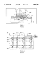
Referring now to FIG. 7, the configuration and operation of word line decoder 606 will be discussed. Specifically, word line decoder 606 is electrically coupled to a global decoder 610 and comprises a partial decoder 702 and a plurality of AND-gates 704. Global decoder 610 receives control signals from a controller and generates a plurality of outputs 706 which act as inputs to AND-gates 704. In accordance with a preferred embodiment of the present invention, global decoder 610 includes 128 outputs 706, one for each sector 300 in block 500.
Similarly, partial decoder 702 receives control signals from the controller and generates a plurality of outputs 708 (preferably 8) which also act as inputs to AND-gates 704. The combination of input signals from global decoder 610 and partial decoder 702 generates signals which control one or more word lines 314 in block 500 (See FIGS. 3-5). In accordance with this aspect of the invention, the output of word line decoder 606 is a plurality of word line connections 710 which are configured to electrically couple to word lines 314. In accordance with a preferred embodiment, word line decoder 606 comprises 1024 word line connections 710; one for each word line 314 in block 500.
For example, for word line decoder 606 to apply a voltage to or "select" the word line WL12 (see FIG. 7), global decoder 610 generates a signal on output 706-2 pursuant to a control signal from the controller. Similarly, partial decoder 702 generates a signal on partial decoder output 708-4. AND-gate 704 combines the two signals and generates a signal on word line connection 710-12 which is coupled to word line WL12. As one skilled in the art will appreciate, a particular AND-gate 704 will not generate an output unless both the global decoder 606 and the partial decoder 702 transmit high voltages to the particular AND-gate.
To select all word lines 314 within a sector, global decoder 606 generates a high voltage signal for the particular sector selected, and all eight partial decoder outputs 708 are sent high. In accordance with this aspect of the invention, the combination of the output(s) from global decoder 606 with the high outputs from partial decoder 702 produces high voltage signals on all word line connection 710 in the selected sector.
In accordance with another aspect of the present invention, the controller for the nonvolatile Flash EEPROM array of the present invention includes circuitry configured to receive externally generated control signals and convert the external signals to internal Flash EEPROM control and data signals. For example, the external signals may be particular address and data signals generated by an Address+Data Pin Interface Protocol. In accordance with this aspect of the present invention, the external address and data signals may be multiplexed into one external signal which can be processed by the control circuitry of the EEPROM array. In addition, the Flash EEPROM control circuitry may be configured to interface with and support MSDOS, MSDOS Disk Internal Operations, ATA signal protocol, PCMCIA/ATA signal protocol, Compact Flash signal protocol, and any other memory access protocols currently known or developed in the future. For a more detailed discussion of these well known protocols and how they interface with EEPROM or Flash EEPROM devices, see for example, AIMS Specification Release 1.01 and PC Card ATA Mass Storage Specification Release 1.02, both of which are incorporated herein by reference.
In accordance with yet a further aspect of the present invention, the control circuitry may comprise an error control circuit implementing a fault tolerance scheme such as a 1-bit error correcting Hamming Code to support fault tolerance in a multiple bit per transistor coding scheme. As one skilled in the art will appreciate, such error control circuits are well known in the art.
In accordance with yet another aspect of the present invention, the Flash EEPROM control circuitry further comprises a cache memory to optimize both read and write operations. For example, to perform a fast read operation, data stored in the flash memory cell can be dumped into the cache memory, and the data subsequently can be read serially from the cache memory. Similarly, to perform a fast write operation, the data to be written to the flash memory cell can be dumped into the cache memory, and the write operation can occur from the cache memory to the flash memory cell.
In accordance with yet a further aspect of the present invention, all the Flash EEPROM control circuitry is fabricated into a single IC chip. In accordance with one embodiment of the invention, the single IC chip may include the cache memory device.
In addition, in accordance with another embodiment of the invention, the nonvolatile Flash EEPROM transistor array of the present invention may be fabricated into the same IC chip as the control circuitry and cache memory. In accordance with this aspect of the invention, one IC chip will include everything necessary to implement the Flash EEPROM array of the present invention.
In conclusion, the present invention comprises a novel EEPROM design configured for implementing nonvolatile memory structures into large arrays which can be used to form hierarchical memory organizations. While the above is a complete description of the preferred embodiments of the invention, various alternatives, modifications, and equivalents may be used. For example, the size of each array, block and/or sector may be altered to achieve specific design considerations. In addition, a different control circuitry design may be utilized to implement the nonvolatile memory array of the present invention. Therefore, the above description should not be taken as limiting the scope of the invention which is defined by the appended claims.

Claims (47)

What is claimed is:
1. A nonvolatile memory device comprising:
a plurality of floating gate transistor cells disposed in a matrix of at least two rows and at least two columns, each floating gate transistor cell having a drain, a source, and a control gate, said drains of each transistor cell in each column being electronically coupled by a first metal, said control gates of each transistor cell in each row being electronically coupled by a second metal, said second metal at least partially forming said control gates of each transistor cell, and all of said sources being electronically coupled by said first metal.
2. The nonvolatile memory device of claim 1 wherein said first metal at least partially forms said drains of each said transistor cell.
3. The nonvolatile memory device of claim 1 wherein said first metal at least partially forms said sources of each said transistor cell.
4. The nonvolatile memory device of claim 1 wherein said first metal and said second metal are generally disposed at a first layer.
5. The nonvolatile memory device of claim 4 wherein each said transistor cell further comprises a floating gate at least partially formed by said second metal.
6. The nonvolatile memory device of claim 5 wherein said second metal at least partially forming said floating gate is disposed at a second layer generally below said second metal disposed at said first layer.
7. The nonvolatile memory device of claim 1 wherein at least a portion of said transistor matrix forms a sector of nonvolatile memory, said sector comprising 8 rows and 512 columns.
8. The nonvolatile memory device of claim 7 wherein a plurality of vertically stacked sectors form a block of nonvolatile memory.
9. The nonvolatile memory device of claim 8 wherein said block comprises 128 sectors.
10. The nonvolatile memory device of claim 7 wherein said nonvolatile memory comprises a plurality of said sectors disposed in a matrix of at least one row and at least on column of said blocks.
11. The nonvolatile memory device of claim 10 further comprising control circuitry comprising at least one word line decoder, at least one source decoder and at least one bit line decoder.
12. The nonvolatile memory device of claim 1 wherein said plurality of floating gate transistor cells comprise MOS NOR-gate transistor cells.
13. The nonvolatile memory device of claim 1 wherein said first metal comprises N+ diffusion and said second metal comprises polysilicon.
14. The nonvolatile memory device of claim 1 wherein said first metal electronically coupling said drains of each transistor cell in each column is a bit line and each said transistor cell coupled to said bit line is controlled by a common bit line driver, a common selector and a common sense amplifier.
15. A nonvolatile NOR-gate transistor matrix comprising:
a plurality of MOS transistor cells disposed in a matrix of at least two rows and at least two columns, each transistor cell having a drain, a source and a control gate, said drains of each transistor cell in each column being electronically coupled, said control gates of each transistor cell in each row being electronically coupled, all of said sources being electronically coupled, and adjacent transistor cells in each column sharing a common well, said common well selected from a group consisting of a common source well and a common drain well.
16. The nonvolatile NOR-gate transistor matrix of claim 15 wherein adjacent transistor cells in each column share at least a common drain well.
17. The nonvolatile NOR-gate transistor matrix of claim 15 wherein adjacent transistor cells in each column share at least a common source well.
18. The nonvolatile NOR-gate transistor matrix of claim 16 wherein said adjacent transistor cells having a common drain well in each column have a common source well with an adjacent transistor cell in each column.
19. The nonvolatile NOR-gate transistor matrix of claim 17 wherein said adjacent transistor cells having a common source well in each column have a common drain well with an adjacent transistor cell in each column.
20. A nonvolatile memory device comprising:
a plurality of MOS NOR-gate transistor cells disposed in a transistor matrix of at least two rows and at least two columns, each transistor cell having a source, a drain and a control gate, said control gates of each transistor cell in a row being electrically coupled, said drains of each transistor cell in each column being electrically coupled, said sources of each transistor cell in a row being electrically coupled by a first metal disposed at a first layer, and all of said sources being electronically coupled by a second metal electrically coupled to said first metal.
21. The nonvolatile memory device of claim 20 wherein said transistor matrix comprises at least one sector of a Flash EEPROM array.
22. The nonvolatile memory device of claim 21 wherein said at least one sector comprises 8 rows and 512 columns.
23. The nonvolatile memory device of claim 21 wherein a plurality of said sectors are stacked vertically forming a block.
24. The nonvolatile memory device of claim 23 wherein said block comprises 128 sectors.
25. The nonvolatile memory device of claim 20 wherein said first metal forms at least part of a well of each said source of each transistor cell.
26. The nonvolatile memory device of claim 20 wherein said first metal forms a first metal line and said second metal forms a second metal line.
27. The nonvolatile memory device of claim 26 wherein said first metal line comprises an N+ diffusion layer.
28. The nonvolatile memory device of claim 27 wherein said first metal line is electrically coupled to said second metal line by metal to N+ diffusion vias.
29. The nonvolatile memory device of claim 26 wherein said second metal line is generally perpendicular to said first metal line.
30. The nonvolatile memory device of claim 20 wherein said second metal is generally disposed at said first layer.
31. The nonvolatile memory device of claim 20 further comprising a third metal electrically coupled to said second metal.
32. The nonvolatile memory device of claim 31 wherein said third metal forms a third metal line.
33. The nonvolatile memory device of claim 32 wherein said third metal line is disposed substantially parallel to said first metal line wherein the resistance of the first metal line is reduced thereby reducing the overall power requirement for said nonvolatile memory device.
34. The nonvolatile memory device of claim 31 wherein said third metal is disposed at a second layer different than said first layer.
35. A nonvolatile memory device comprising:
a plurality of floating gate transistor cells disposed in a matrix of at least two rows and two columns, each transistor cell in a column sharing at least one common region, said common region selected from a group consisting of a source region and a drain region, said source region and said drain region comprising a first conductive material.
36. The nonvolatile memory device of claim 35 wherein said floating gate transistor cells are disposed in a matrix of 8 rows and 512 columns.
37. The nonvolatile memory device of claim 36 wherein six of said floating gate transistor cells disposed in a column share both a source region and a drain region with an adjacent transistor cell.
38. The nonvolatile memory device of claim 35 wherein each floating gate transistor has a source, a drain and a control gate, said drains of each transistor in a column being electronically coupled, said control gates of each transistor in a row being electronically coupled, and all of said sources being electronically coupled.
39. The nonvolatile memory device of claim 35 wherein said first conductive material comprises N+ diffusion.
40. The nonvolatile memory device of claim 35 wherein at least one of said floating gate transistor cells disposed in a column share both a source region and a drain region with an adjacent transistor cell.
41. A nonvolatile memory device comprising:
a plurality of sectors each comprising a plurality of floating gate transistor cells disposed in a matrix of 8 rows and 512 columns, each floating gate transistor cell having a drain, a source and a control gate, said drains of each transistor cell in each column being electronically coupled by a first metal, said control gates of each transistor cell in each row being electronically coupled by a second metal, and all of said sources being electronically coupled by said first metal.
42. The nonvolatile memory device of claim 41 wherein said drain of each transistor in each column in vertically stacked sectors is coupled to drains in corresponding columns of transistors in vertically adjacent sectors.
43. The nonvolatile memory device of claim 41 wherein said plurality of sectors form one or more blocks, each of said blocks comprising two or more of said plurality of sectors vertically stacked.
44. The nonvolatile memory device of claim 43 wherein each of said one or more blocks comprises 128 vertically stacked sectors.
45. The nonvolatile memory device of claim 43 wherein each of said one or more blocks are arranged in a matrix of at least one row and at least one column comprising a nonvolatile Flash EEPROM array.
46. The nonvolatile memory device of claim 43 further comprising control circuitry comprising at least one source decoder, at least one bit line decoder and at least one word line decoder.
47. The nonvolatile memory device of claim 46 wherein said word line decoder comprises a partial decoder and a plurality of AND gates, said partial decoder configured to receive control signals from a controller and to generate a plurality of outputs which comprise inputs to said AND gates, the output of said word line decoder coupled to word lines in said block.
US09/345,086 1997-02-12 1999-06-30 Non-volatile memory structure Expired - Lifetime US6084798A (en)

Priority Applications (1)

Application Number Priority Date Filing Date Title
US09/345,086 US6084798A (en) 1997-02-12 1999-06-30 Non-volatile memory structure

Applications Claiming Priority (3)

Application Number Priority Date Filing Date Title
US3791197P 1997-02-12 1997-02-12
US09/023,019 US5956268A (en) 1997-02-12 1998-02-11 Nonvolatile memory structure
US09/345,086 US6084798A (en) 1997-02-12 1999-06-30 Non-volatile memory structure

Related Parent Applications (1)

Application Number Title Priority Date Filing Date
US09/023,019 Continuation US5956268A (en) 1997-02-12 1998-02-11 Nonvolatile memory structure

Publications (1)

Publication Number Publication Date
US6084798A true US6084798A (en) 2000-07-04

Family

ID=21897018

Family Applications (2)

Application Number Title Priority Date Filing Date
US09/023,019 Expired - Lifetime US5956268A (en) 1997-02-12 1998-02-11 Nonvolatile memory structure
US09/345,086 Expired - Lifetime US6084798A (en) 1997-02-12 1999-06-30 Non-volatile memory structure

Family Applications Before (1)

Application Number Title Priority Date Filing Date
US09/023,019 Expired - Lifetime US5956268A (en) 1997-02-12 1998-02-11 Nonvolatile memory structure

Country Status (6)

Country Link
US (2) US5956268A (en)
JP (1) JP2000504504A (en)
KR (1) KR100323970B1 (en)
DE (1) DE19880311B3 (en)
GB (1) GB2326748B (en)
WO (1) WO1998035344A2 (en)

Cited By (6)

* Cited by examiner, † Cited by third party
Publication number Priority date Publication date Assignee Title
US20020003270A1 (en) * 2000-07-10 2002-01-10 Mitsubishi Denki Kabushiki Kaisha Semiconductor device
US20030235949A1 (en) * 2002-06-24 2003-12-25 Texas Instruments Incorporated Memory device with reduced cell size
US20040246778A1 (en) * 2002-06-28 2004-12-09 Tsu-Jae King Two terminal silicon based negative differential resistance device
US20050078528A1 (en) * 2003-10-14 2005-04-14 Tsang Sai K. Group erasing system for flash array with multiple sectors
US7512015B1 (en) 2006-07-17 2009-03-31 Lattice Semiconductor Corporation Negative voltage blocking for embedded memories
US7636259B1 (en) 2006-07-17 2009-12-22 Lallice Semiconductor Corporation Flash memory array with independently erasable sectors

Families Citing this family (84)

* Cited by examiner, † Cited by third party
Publication number Priority date Publication date Assignee Title
JP2000504504A (en) * 1997-02-12 2000-04-11 ヒュンダイ エレクトロニクス アメリカ インコーポレイテッド Non-volatile memory structure
US6033955A (en) * 1998-09-23 2000-03-07 Advanced Micro Devices, Inc. Method of making flexibly partitioned metal line segments for a simultaneous operation flash memory device with a flexible bank partition architecture
DE69832609D1 (en) * 1998-09-30 2006-01-05 St Microelectronics Srl Emulated EEPROM memory device and corresponding method
US6466476B1 (en) 2001-01-18 2002-10-15 Multi Level Memory Technology Data coding for multi-bit-per-cell memories having variable numbers of bits per memory cell
US6958940B2 (en) * 2002-02-28 2005-10-25 Renesas Technology Corp. Nonvolatile semiconductor memory device capable of realizing optimized erasing operation in a memory array
US6795348B2 (en) * 2002-05-29 2004-09-21 Micron Technology, Inc. Method and apparatus for erasing flash memory
JP2004021956A (en) * 2002-06-12 2004-01-22 Jenoa:Kk Portable storage medium provided with access restriction circuit
US6850438B2 (en) * 2002-07-05 2005-02-01 Aplus Flash Technology, Inc. Combination nonvolatile memory using unified technology with byte, page and block write and simultaneous read and write operations
ITMI20022240A1 (en) * 2002-10-22 2004-04-23 Atmel Corp FLASH MEMORY ARCHITECTURE WITH MODE CANCELLATION
KR100546342B1 (en) * 2003-07-12 2006-01-26 삼성전자주식회사 Row decoder providing for improved layout of repetitively disposed pre-decoded signal lines, semiconductor memory device having it, and method thereof
JP4768504B2 (en) * 2006-04-28 2011-09-07 株式会社東芝 Storage device using nonvolatile flash memory
US8365040B2 (en) 2007-09-20 2013-01-29 Densbits Technologies Ltd. Systems and methods for handling immediate data errors in flash memory
US8650352B2 (en) 2007-09-20 2014-02-11 Densbits Technologies Ltd. Systems and methods for determining logical values of coupled flash memory cells
US8694715B2 (en) 2007-10-22 2014-04-08 Densbits Technologies Ltd. Methods for adaptively programming flash memory devices and flash memory systems incorporating same
WO2009053961A2 (en) 2007-10-25 2009-04-30 Densbits Technologies Ltd. Systems and methods for multiple coding rates in flash devices
WO2009072104A2 (en) 2007-12-05 2009-06-11 Densbits Technologies Ltd. Flash memory device with physical cell value deterioration accommodation and methods useful in conjunction therewith
US8607128B2 (en) 2007-12-05 2013-12-10 Densbits Technologies Ltd. Low power chien-search based BCH/RS decoding system for flash memory, mobile communications devices and other applications
WO2009072103A2 (en) 2007-12-05 2009-06-11 Densbits Technologies Ltd. Flash memory apparatus and methods using a plurality of decoding stages including optional use of concatenated bch codes and/or designation of 'first below' cells
WO2009074978A2 (en) 2007-12-12 2009-06-18 Densbits Technologies Ltd. Systems and methods for error correction and decoding on multi-level physical media
WO2009074979A2 (en) * 2007-12-12 2009-06-18 Densbits Technologies Ltd. Chien-search system employing a clock-gating scheme to save power for error correction decoder and other applications
US8327246B2 (en) 2007-12-18 2012-12-04 Densbits Technologies Ltd. Apparatus for coding at a plurality of rates in multi-level flash memory systems, and methods useful in conjunction therewith
WO2009118720A2 (en) 2008-03-25 2009-10-01 Densbits Technologies Ltd. Apparatus and methods for hardware-efficient unbiased rounding
US8332725B2 (en) * 2008-08-20 2012-12-11 Densbits Technologies Ltd. Reprogramming non volatile memory portions
US8458574B2 (en) 2009-04-06 2013-06-04 Densbits Technologies Ltd. Compact chien-search based decoding apparatus and method
US8819385B2 (en) 2009-04-06 2014-08-26 Densbits Technologies Ltd. Device and method for managing a flash memory
US8566510B2 (en) 2009-05-12 2013-10-22 Densbits Technologies Ltd. Systems and method for flash memory management
US8305812B2 (en) 2009-08-26 2012-11-06 Densbits Technologies Ltd. Flash memory module and method for programming a page of flash memory cells
US8868821B2 (en) 2009-08-26 2014-10-21 Densbits Technologies Ltd. Systems and methods for pre-equalization and code design for a flash memory
US8995197B1 (en) 2009-08-26 2015-03-31 Densbits Technologies Ltd. System and methods for dynamic erase and program control for flash memory device memories
US9330767B1 (en) 2009-08-26 2016-05-03 Avago Technologies General Ip (Singapore) Pte. Ltd. Flash memory module and method for programming a page of flash memory cells
US8730729B2 (en) 2009-10-15 2014-05-20 Densbits Technologies Ltd. Systems and methods for averaging error rates in non-volatile devices and storage systems
US8724387B2 (en) 2009-10-22 2014-05-13 Densbits Technologies Ltd. Method, system, and computer readable medium for reading and programming flash memory cells using multiple bias voltages
US8626988B2 (en) 2009-11-19 2014-01-07 Densbits Technologies Ltd. System and method for uncoded bit error rate equalization via interleaving
US9037777B2 (en) 2009-12-22 2015-05-19 Densbits Technologies Ltd. Device, system, and method for reducing program/read disturb in flash arrays
US8607124B2 (en) 2009-12-24 2013-12-10 Densbits Technologies Ltd. System and method for setting a flash memory cell read threshold
US8700970B2 (en) 2010-02-28 2014-04-15 Densbits Technologies Ltd. System and method for multi-dimensional decoding
US9104610B2 (en) 2010-04-06 2015-08-11 Densbits Technologies Ltd. Method, system and medium for analog encryption in a flash memory
US8527840B2 (en) 2010-04-06 2013-09-03 Densbits Technologies Ltd. System and method for restoring damaged data programmed on a flash device
US8745317B2 (en) 2010-04-07 2014-06-03 Densbits Technologies Ltd. System and method for storing information in a multi-level cell memory
US9021177B2 (en) 2010-04-29 2015-04-28 Densbits Technologies Ltd. System and method for allocating and using spare blocks in a flash memory
US8539311B2 (en) 2010-07-01 2013-09-17 Densbits Technologies Ltd. System and method for data recovery in multi-level cell memories
US8468431B2 (en) 2010-07-01 2013-06-18 Densbits Technologies Ltd. System and method for multi-dimensional encoding and decoding
US8467249B2 (en) 2010-07-06 2013-06-18 Densbits Technologies Ltd. Systems and methods for storing, retrieving, and adjusting read thresholds in flash memory storage system
US8964464B2 (en) 2010-08-24 2015-02-24 Densbits Technologies Ltd. System and method for accelerated sampling
US8508995B2 (en) 2010-09-15 2013-08-13 Densbits Technologies Ltd. System and method for adjusting read voltage thresholds in memories
US9063878B2 (en) 2010-11-03 2015-06-23 Densbits Technologies Ltd. Method, system and computer readable medium for copy back
US8850100B2 (en) 2010-12-07 2014-09-30 Densbits Technologies Ltd. Interleaving codeword portions between multiple planes and/or dies of a flash memory device
US10079068B2 (en) 2011-02-23 2018-09-18 Avago Technologies General Ip (Singapore) Pte. Ltd. Devices and method for wear estimation based memory management
US8693258B2 (en) 2011-03-17 2014-04-08 Densbits Technologies Ltd. Obtaining soft information using a hard interface
US8990665B1 (en) 2011-04-06 2015-03-24 Densbits Technologies Ltd. System, method and computer program product for joint search of a read threshold and soft decoding
US9501392B1 (en) 2011-05-12 2016-11-22 Avago Technologies General Ip (Singapore) Pte. Ltd. Management of a non-volatile memory module
US9372792B1 (en) 2011-05-12 2016-06-21 Avago Technologies General Ip (Singapore) Pte. Ltd. Advanced management of a non-volatile memory
US8996790B1 (en) 2011-05-12 2015-03-31 Densbits Technologies Ltd. System and method for flash memory management
US9396106B2 (en) 2011-05-12 2016-07-19 Avago Technologies General Ip (Singapore) Pte. Ltd. Advanced management of a non-volatile memory
US9110785B1 (en) 2011-05-12 2015-08-18 Densbits Technologies Ltd. Ordered merge of data sectors that belong to memory space portions
US9195592B1 (en) 2011-05-12 2015-11-24 Densbits Technologies Ltd. Advanced management of a non-volatile memory
US8667211B2 (en) 2011-06-01 2014-03-04 Densbits Technologies Ltd. System and method for managing a non-volatile memory
US8588003B1 (en) 2011-08-01 2013-11-19 Densbits Technologies Ltd. System, method and computer program product for programming and for recovering from a power failure
US8553468B2 (en) 2011-09-21 2013-10-08 Densbits Technologies Ltd. System and method for managing erase operations in a non-volatile memory
US8996788B2 (en) 2012-02-09 2015-03-31 Densbits Technologies Ltd. Configurable flash interface
US8947941B2 (en) 2012-02-09 2015-02-03 Densbits Technologies Ltd. State responsive operations relating to flash memory cells
US8996793B1 (en) 2012-04-24 2015-03-31 Densbits Technologies Ltd. System, method and computer readable medium for generating soft information
US8838937B1 (en) 2012-05-23 2014-09-16 Densbits Technologies Ltd. Methods, systems and computer readable medium for writing and reading data
US8879325B1 (en) 2012-05-30 2014-11-04 Densbits Technologies Ltd. System, method and computer program product for processing read threshold information and for reading a flash memory module
US9921954B1 (en) 2012-08-27 2018-03-20 Avago Technologies General Ip (Singapore) Pte. Ltd. Method and system for split flash memory management between host and storage controller
US9368225B1 (en) 2012-11-21 2016-06-14 Avago Technologies General Ip (Singapore) Pte. Ltd. Determining read thresholds based upon read error direction statistics
US9069659B1 (en) 2013-01-03 2015-06-30 Densbits Technologies Ltd. Read threshold determination using reference read threshold
US9136876B1 (en) 2013-06-13 2015-09-15 Densbits Technologies Ltd. Size limited multi-dimensional decoding
US9413491B1 (en) 2013-10-08 2016-08-09 Avago Technologies General Ip (Singapore) Pte. Ltd. System and method for multiple dimension decoding and encoding a message
US9348694B1 (en) 2013-10-09 2016-05-24 Avago Technologies General Ip (Singapore) Pte. Ltd. Detecting and managing bad columns
US9397706B1 (en) 2013-10-09 2016-07-19 Avago Technologies General Ip (Singapore) Pte. Ltd. System and method for irregular multiple dimension decoding and encoding
US9786388B1 (en) 2013-10-09 2017-10-10 Avago Technologies General Ip (Singapore) Pte. Ltd. Detecting and managing bad columns
US9536612B1 (en) 2014-01-23 2017-01-03 Avago Technologies General Ip (Singapore) Pte. Ltd Digital signaling processing for three dimensional flash memory arrays
US10120792B1 (en) 2014-01-29 2018-11-06 Avago Technologies General Ip (Singapore) Pte. Ltd. Programming an embedded flash storage device
US9542262B1 (en) 2014-05-29 2017-01-10 Avago Technologies General Ip (Singapore) Pte. Ltd. Error correction
US9892033B1 (en) 2014-06-24 2018-02-13 Avago Technologies General Ip (Singapore) Pte. Ltd. Management of memory units
US9972393B1 (en) 2014-07-03 2018-05-15 Avago Technologies General Ip (Singapore) Pte. Ltd. Accelerating programming of a flash memory module
US9584159B1 (en) 2014-07-03 2017-02-28 Avago Technologies General Ip (Singapore) Pte. Ltd. Interleaved encoding
US9449702B1 (en) 2014-07-08 2016-09-20 Avago Technologies General Ip (Singapore) Pte. Ltd. Power management
US9524211B1 (en) 2014-11-18 2016-12-20 Avago Technologies General Ip (Singapore) Pte. Ltd. Codeword management
US10305515B1 (en) 2015-02-02 2019-05-28 Avago Technologies International Sales Pte. Limited System and method for encoding using multiple linear feedback shift registers
US10628255B1 (en) 2015-06-11 2020-04-21 Avago Technologies International Sales Pte. Limited Multi-dimensional decoding
US9851921B1 (en) 2015-07-05 2017-12-26 Avago Technologies General Ip (Singapore) Pte. Ltd. Flash memory chip processing
US9954558B1 (en) 2016-03-03 2018-04-24 Avago Technologies General Ip (Singapore) Pte. Ltd. Fast decoding of data stored in a flash memory

Citations (9)

* Cited by examiner, † Cited by third party
Publication number Priority date Publication date Assignee Title
US5278785A (en) * 1988-02-05 1994-01-11 Emanuel Hazani Non-volatile memory circuits and architecture
US5315541A (en) * 1992-07-24 1994-05-24 Sundisk Corporation Segmented column memory array
US5345416A (en) * 1991-08-29 1994-09-06 Sony Corporation High density nonvolatile memory and decoder of the same
US5546339A (en) * 1993-10-29 1996-08-13 Nec Corporation Nonvolatile semiconductor memory device equipped with means for suppressing drain disturbance phenomenon
US5592419A (en) * 1991-12-09 1997-01-07 Fujitsu Limited Flash memory with improved erasability and its circuitry
US5646888A (en) * 1993-02-26 1997-07-08 Kabushiki Kaisha Toshiba Semiconductor device having isolating regions
US5781476A (en) * 1989-02-06 1998-07-14 Hitachi, Ltd. Nonvolatile semiconductor memory device
US5889699A (en) * 1996-02-26 1999-03-30 Sanyo Electric Co., Ltd. Non-volatile semiconductor memory device
US5956268A (en) * 1997-02-12 1999-09-21 Hyundai Electronics America Nonvolatile memory structure

Family Cites Families (38)

* Cited by examiner, † Cited by third party
Publication number Priority date Publication date Assignee Title
JP3059442B2 (en) * 1988-11-09 2000-07-04 株式会社日立製作所 Semiconductor storage device
JP2732601B2 (en) * 1987-11-18 1998-03-30 株式会社東芝 Nonvolatile semiconductor memory device
US5198380A (en) * 1988-06-08 1993-03-30 Sundisk Corporation Method of highly compact EPROM and flash EEPROM devices
US5315547A (en) * 1988-07-11 1994-05-24 Hitachi, Ltd. Nonvolatile semiconductor memory device with selective tow erasure
EP0617363B1 (en) * 1989-04-13 2000-01-26 SanDisk Corporation Defective cell substitution in EEprom array
US5535328A (en) * 1989-04-13 1996-07-09 Sandisk Corporation Non-volatile memory system card with flash erasable sectors of EEprom cells including a mechanism for substituting defective cells
US5172338B1 (en) * 1989-04-13 1997-07-08 Sandisk Corp Multi-state eeprom read and write circuits and techniques
US5126808A (en) * 1989-10-23 1992-06-30 Advanced Micro Devices, Inc. Flash EEPROM array with paged erase architecture
EP0550751B1 (en) * 1990-09-25 1998-01-07 Kabushiki Kaisha Toshiba Nonvolatile semiconductor memory
JP3204666B2 (en) * 1990-11-21 2001-09-04 株式会社東芝 Nonvolatile semiconductor memory device
GB2251324B (en) * 1990-12-31 1995-05-10 Intel Corp File structure for a non-volatile semiconductor memory
US5191556A (en) * 1991-03-13 1993-03-02 Advanced Micro Devices, Inc. Method of page-mode programming flash eeprom cell arrays
JPH04311897A (en) * 1991-04-11 1992-11-04 Toshiba Corp Semiconductor memory
EP0520505B1 (en) * 1991-06-27 1997-03-05 Kabushiki Kaisha Toshiba Nonvolatile semiconductor memory device and its operating method
US5359569A (en) * 1991-10-29 1994-10-25 Hitachi Ltd. Semiconductor memory
JP3178909B2 (en) * 1992-01-10 2001-06-25 株式会社東芝 Semiconductor memory device
JP2904645B2 (en) * 1992-05-28 1999-06-14 株式会社東芝 Non-volatile semiconductor memory
JP3328321B2 (en) * 1992-06-22 2002-09-24 株式会社日立製作所 Semiconductor storage device
KR960006272B1 (en) * 1992-09-04 1996-05-13 삼성전자주식회사 Flash write circuit of semiconductor memory device
US5581723A (en) * 1993-02-19 1996-12-03 Intel Corporation Method and apparatus for retaining flash block structure data during erase operations in a flash EEPROM memory array
JP2839819B2 (en) * 1993-05-28 1998-12-16 株式会社東芝 Nonvolatile semiconductor memory device
US5592641A (en) * 1993-06-30 1997-01-07 Intel Corporation Method and device for selectively locking write access to blocks in a memory array using write protect inputs and block enabled status
US5422842A (en) * 1993-07-08 1995-06-06 Sundisk Corporation Method and circuit for simultaneously programming and verifying the programming of selected EEPROM cells
US5365484A (en) * 1993-08-23 1994-11-15 Advanced Micro Devices, Inc. Independent array grounds for flash EEPROM array with paged erase architechture
US5349558A (en) * 1993-08-26 1994-09-20 Advanced Micro Devices, Inc. Sector-based redundancy architecture
US5537350A (en) * 1993-09-10 1996-07-16 Intel Corporation Method and apparatus for sequential programming of the bits in a word of a flash EEPROM memory array
US5477499A (en) * 1993-10-13 1995-12-19 Advanced Micro Devices, Inc. Memory architecture for a three volt flash EEPROM
JPH07253929A (en) * 1994-03-14 1995-10-03 Hitachi Ltd Semiconductor storage device
US5603001A (en) * 1994-05-09 1997-02-11 Kabushiki Kaisha Toshiba Semiconductor disk system having a plurality of flash memories
US5523972A (en) * 1994-06-02 1996-06-04 Intel Corporation Method and apparatus for verifying the programming of multi-level flash EEPROM memory
EP0690452A3 (en) * 1994-06-28 1999-01-07 Advanced Micro Devices, Inc. Electrically erasable memory and method of erasure
KR0144818B1 (en) * 1994-07-25 1998-08-17 김광호 Nand type flash memory ic card
US5606529A (en) * 1994-12-20 1997-02-25 Hitachi, Ltd. Semiconductor disk storage
US5541886A (en) * 1994-12-27 1996-07-30 Intel Corporation Method and apparatus for storing control information in multi-bit non-volatile memory arrays
US5491657A (en) * 1995-02-24 1996-02-13 Advanced Micro Devices, Inc. Method for bulk (or byte) charging and discharging an array of flash EEPROM memory cells
US5579259A (en) * 1995-05-31 1996-11-26 Sandisk Corporation Low voltage erase of a flash EEPROM system having a common erase electrode for two individually erasable sectors
US5657268A (en) * 1995-11-20 1997-08-12 Texas Instruments Incorporated Array-source line, bitline and wordline sequence in flash operations
US5682350A (en) * 1996-03-29 1997-10-28 Aplus Integrated Circuits, Inc. Flash memory with divided bitline

Patent Citations (9)

* Cited by examiner, † Cited by third party
Publication number Priority date Publication date Assignee Title
US5278785A (en) * 1988-02-05 1994-01-11 Emanuel Hazani Non-volatile memory circuits and architecture
US5781476A (en) * 1989-02-06 1998-07-14 Hitachi, Ltd. Nonvolatile semiconductor memory device
US5345416A (en) * 1991-08-29 1994-09-06 Sony Corporation High density nonvolatile memory and decoder of the same
US5592419A (en) * 1991-12-09 1997-01-07 Fujitsu Limited Flash memory with improved erasability and its circuitry
US5315541A (en) * 1992-07-24 1994-05-24 Sundisk Corporation Segmented column memory array
US5646888A (en) * 1993-02-26 1997-07-08 Kabushiki Kaisha Toshiba Semiconductor device having isolating regions
US5546339A (en) * 1993-10-29 1996-08-13 Nec Corporation Nonvolatile semiconductor memory device equipped with means for suppressing drain disturbance phenomenon
US5889699A (en) * 1996-02-26 1999-03-30 Sanyo Electric Co., Ltd. Non-volatile semiconductor memory device
US5956268A (en) * 1997-02-12 1999-09-21 Hyundai Electronics America Nonvolatile memory structure

Cited By (8)

* Cited by examiner, † Cited by third party
Publication number Priority date Publication date Assignee Title
US20020003270A1 (en) * 2000-07-10 2002-01-10 Mitsubishi Denki Kabushiki Kaisha Semiconductor device
US6635935B2 (en) * 2000-07-10 2003-10-21 Mitsubishi Denki Kabushiki Kaisha Semiconductor device cell having regularly sized and arranged features
US20030235949A1 (en) * 2002-06-24 2003-12-25 Texas Instruments Incorporated Memory device with reduced cell size
US6958269B2 (en) * 2002-06-24 2005-10-25 Texas Instruments Incorporated Memory device with reduced cell size
US20040246778A1 (en) * 2002-06-28 2004-12-09 Tsu-Jae King Two terminal silicon based negative differential resistance device
US20050078528A1 (en) * 2003-10-14 2005-04-14 Tsang Sai K. Group erasing system for flash array with multiple sectors
US7512015B1 (en) 2006-07-17 2009-03-31 Lattice Semiconductor Corporation Negative voltage blocking for embedded memories
US7636259B1 (en) 2006-07-17 2009-12-22 Lallice Semiconductor Corporation Flash memory array with independently erasable sectors

Also Published As

Publication number Publication date
JP2000504504A (en) 2000-04-11
US5956268A (en) 1999-09-21
GB2326748B (en) 2001-09-12
KR100323970B1 (en) 2002-03-08
WO1998035344A2 (en) 1998-08-13
DE19880311T1 (en) 1999-05-12
GB9820270D0 (en) 1998-11-11
KR20000064879A (en) 2000-11-06
DE19880311B3 (en) 2017-06-22
WO1998035344A3 (en) 1998-12-17
GB2326748A (en) 1998-12-30

Similar Documents

Publication Publication Date Title
US6084798A (en) Non-volatile memory structure
US6850438B2 (en) Combination nonvolatile memory using unified technology with byte, page and block write and simultaneous read and write operations
US5798968A (en) Plane decode/virtual sector architecture
US5270980A (en) Sector erasable flash EEPROM
US6532172B2 (en) Steering gate and bit line segmentation in non-volatile memories
US6181597B1 (en) EEPROM array using 2-bit non-volatile memory cells with serial read operations
US6954382B2 (en) Multiple use memory chip
KR100187196B1 (en) Non-volatile semiconductor memory device
KR960001320B1 (en) Semiconductor memory device
US5815441A (en) Non-volatile semiconductor memory device
JP2002313090A5 (en)
KR100639827B1 (en) 1 transistor cell for eeprom application
US6487125B2 (en) Integrated circuit having an EEPROM and flash EPROM
US6697281B2 (en) Byte-selectable EEPROM array utilizing single split-gate transistor for non-volatile storage cell
JP3540881B2 (en) Writing method for nonvolatile semiconductor memory device
JPH07169288A (en) Batch erasing type non-volatile memory
JP3362917B2 (en) Semiconductor memory device

Legal Events

Date Code Title Description
STCF Information on status: patent grant

Free format text: PATENTED CASE

FEPP Fee payment procedure

Free format text: PAYOR NUMBER ASSIGNED (ORIGINAL EVENT CODE: ASPN); ENTITY STATUS OF PATENT OWNER: LARGE ENTITY

FEPP Fee payment procedure

Free format text: PAYER NUMBER DE-ASSIGNED (ORIGINAL EVENT CODE: RMPN); ENTITY STATUS OF PATENT OWNER: LARGE ENTITY

Free format text: PAYOR NUMBER ASSIGNED (ORIGINAL EVENT CODE: ASPN); ENTITY STATUS OF PATENT OWNER: LARGE ENTITY

FPAY Fee payment

Year of fee payment: 4

FPAY Fee payment

Year of fee payment: 8

FEPP Fee payment procedure

Free format text: PAYER NUMBER DE-ASSIGNED (ORIGINAL EVENT CODE: RMPN); ENTITY STATUS OF PATENT OWNER: LARGE ENTITY

Free format text: PAYOR NUMBER ASSIGNED (ORIGINAL EVENT CODE: ASPN); ENTITY STATUS OF PATENT OWNER: LARGE ENTITY

FPAY Fee payment

Year of fee payment: 12