US6091152A - Semiconductor device and method for fabricating the same - Google Patents
Semiconductor device and method for fabricating the same Download PDFInfo
- Publication number
- US6091152A US6091152A US09/073,272 US7327298A US6091152A US 6091152 A US6091152 A US 6091152A US 7327298 A US7327298 A US 7327298A US 6091152 A US6091152 A US 6091152A
- Authority
- US
- United States
- Prior art keywords
- film
- titanium
- silicon
- tisi
- silicide film
- Prior art date
- Legal status (The legal status is an assumption and is not a legal conclusion. Google has not performed a legal analysis and makes no representation as to the accuracy of the status listed.)
- Expired - Lifetime
Links
- 239000004065 semiconductor Substances 0.000 title claims abstract description 29
- 238000000034 method Methods 0.000 title abstract description 70
- 229910021332 silicide Inorganic materials 0.000 claims abstract description 29
- FVBUAEGBCNSCDD-UHFFFAOYSA-N silicide(4-) Chemical compound [Si-4] FVBUAEGBCNSCDD-UHFFFAOYSA-N 0.000 claims abstract description 29
- 229910021341 titanium silicide Inorganic materials 0.000 claims description 88
- 229910008479 TiSi2 Inorganic materials 0.000 claims description 63
- DFJQEGUNXWZVAH-UHFFFAOYSA-N bis($l^{2}-silanylidene)titanium Chemical compound [Si]=[Ti]=[Si] DFJQEGUNXWZVAH-UHFFFAOYSA-N 0.000 claims description 61
- NRTOMJZYCJJWKI-UHFFFAOYSA-N Titanium nitride Chemical compound [Ti]#N NRTOMJZYCJJWKI-UHFFFAOYSA-N 0.000 claims description 49
- 239000013078 crystal Substances 0.000 claims description 32
- 229910052710 silicon Inorganic materials 0.000 abstract description 111
- 239000010703 silicon Substances 0.000 abstract description 104
- XUIMIQQOPSSXEZ-UHFFFAOYSA-N Silicon Chemical compound [Si] XUIMIQQOPSSXEZ-UHFFFAOYSA-N 0.000 abstract description 93
- 229910052760 oxygen Inorganic materials 0.000 abstract description 56
- QVGXLLKOCUKJST-UHFFFAOYSA-N atomic oxygen Chemical compound [O] QVGXLLKOCUKJST-UHFFFAOYSA-N 0.000 abstract description 51
- 239000001301 oxygen Substances 0.000 abstract description 51
- 229910052751 metal Inorganic materials 0.000 abstract description 24
- 239000002184 metal Substances 0.000 abstract description 24
- 238000000151 deposition Methods 0.000 abstract description 23
- 239000010936 titanium Substances 0.000 description 70
- 229910052719 titanium Inorganic materials 0.000 description 65
- RTAQQCXQSZGOHL-UHFFFAOYSA-N Titanium Chemical compound [Ti] RTAQQCXQSZGOHL-UHFFFAOYSA-N 0.000 description 59
- IJGRMHOSHXDMSA-UHFFFAOYSA-N Atomic nitrogen Chemical compound N#N IJGRMHOSHXDMSA-UHFFFAOYSA-N 0.000 description 53
- 238000004151 rapid thermal annealing Methods 0.000 description 41
- VYPSYNLAJGMNEJ-UHFFFAOYSA-N Silicium dioxide Chemical compound O=[Si]=O VYPSYNLAJGMNEJ-UHFFFAOYSA-N 0.000 description 36
- 238000006243 chemical reaction Methods 0.000 description 34
- 229910021420 polycrystalline silicon Inorganic materials 0.000 description 33
- 239000000758 substrate Substances 0.000 description 31
- 238000007796 conventional method Methods 0.000 description 27
- 238000000137 annealing Methods 0.000 description 25
- ATJFFYVFTNAWJD-UHFFFAOYSA-N Tin Chemical compound [Sn] ATJFFYVFTNAWJD-UHFFFAOYSA-N 0.000 description 24
- 229910052718 tin Inorganic materials 0.000 description 24
- 229910052757 nitrogen Inorganic materials 0.000 description 20
- 238000005530 etching Methods 0.000 description 19
- XKRFYHLGVUSROY-UHFFFAOYSA-N Argon Chemical compound [Ar] XKRFYHLGVUSROY-UHFFFAOYSA-N 0.000 description 18
- 229910052681 coesite Inorganic materials 0.000 description 18
- 229910052906 cristobalite Inorganic materials 0.000 description 18
- 229910001873 dinitrogen Inorganic materials 0.000 description 18
- 239000000377 silicon dioxide Substances 0.000 description 18
- 229910052682 stishovite Inorganic materials 0.000 description 18
- 229910052905 tridymite Inorganic materials 0.000 description 18
- 238000004544 sputter deposition Methods 0.000 description 17
- KRHYYFGTRYWZRS-UHFFFAOYSA-N Fluorane Chemical compound F KRHYYFGTRYWZRS-UHFFFAOYSA-N 0.000 description 16
- 239000007789 gas Substances 0.000 description 16
- -1 Arsenic ions Chemical class 0.000 description 15
- 238000004518 low pressure chemical vapour deposition Methods 0.000 description 15
- 229910021417 amorphous silicon Inorganic materials 0.000 description 14
- 238000005054 agglomeration Methods 0.000 description 13
- 230000002776 aggregation Effects 0.000 description 13
- 238000004140 cleaning Methods 0.000 description 11
- 230000008569 process Effects 0.000 description 10
- 239000000243 solution Substances 0.000 description 10
- 239000012212 insulator Substances 0.000 description 9
- 238000005468 ion implantation Methods 0.000 description 9
- 239000000370 acceptor Substances 0.000 description 8
- 230000004913 activation Effects 0.000 description 8
- 229910052786 argon Inorganic materials 0.000 description 8
- 239000012535 impurity Substances 0.000 description 8
- 238000004519 manufacturing process Methods 0.000 description 8
- 125000006850 spacer group Chemical group 0.000 description 8
- GWEVSGVZZGPLCZ-UHFFFAOYSA-N Titan oxide Chemical compound O=[Ti]=O GWEVSGVZZGPLCZ-UHFFFAOYSA-N 0.000 description 6
- 230000015572 biosynthetic process Effects 0.000 description 6
- 150000002500 ions Chemical class 0.000 description 6
- 230000007704 transition Effects 0.000 description 6
- 239000000203 mixture Substances 0.000 description 5
- QAOWNCQODCNURD-UHFFFAOYSA-N Sulfuric acid Chemical compound OS(O)(=O)=O QAOWNCQODCNURD-UHFFFAOYSA-N 0.000 description 4
- 230000008021 deposition Effects 0.000 description 4
- 238000002513 implantation Methods 0.000 description 4
- 238000001953 recrystallisation Methods 0.000 description 4
- 230000009467 reduction Effects 0.000 description 4
- UFHFLCQGNIYNRP-UHFFFAOYSA-N Hydrogen Chemical compound [H][H] UFHFLCQGNIYNRP-UHFFFAOYSA-N 0.000 description 3
- 230000008859 change Effects 0.000 description 3
- 238000009792 diffusion process Methods 0.000 description 3
- 238000002474 experimental method Methods 0.000 description 3
- 239000001257 hydrogen Substances 0.000 description 3
- 229910052739 hydrogen Inorganic materials 0.000 description 3
- 229920002120 photoresistant polymer Polymers 0.000 description 3
- 238000005546 reactive sputtering Methods 0.000 description 3
- 238000001004 secondary ion mass spectrometry Methods 0.000 description 3
- 235000017166 Bambusa arundinacea Nutrition 0.000 description 2
- 235000017491 Bambusa tulda Nutrition 0.000 description 2
- 241001330002 Bambuseae Species 0.000 description 2
- MHAJPDPJQMAIIY-UHFFFAOYSA-N Hydrogen peroxide Chemical compound OO MHAJPDPJQMAIIY-UHFFFAOYSA-N 0.000 description 2
- 235000015334 Phyllostachys viridis Nutrition 0.000 description 2
- BLRPTPMANUNPDV-UHFFFAOYSA-N Silane Chemical compound [SiH4] BLRPTPMANUNPDV-UHFFFAOYSA-N 0.000 description 2
- 229910008484 TiSi Inorganic materials 0.000 description 2
- 238000004458 analytical method Methods 0.000 description 2
- 229910052785 arsenic Inorganic materials 0.000 description 2
- 239000011425 bamboo Substances 0.000 description 2
- 230000008901 benefit Effects 0.000 description 2
- 230000003749 cleanliness Effects 0.000 description 2
- 229910021419 crystalline silicon Inorganic materials 0.000 description 2
- 230000006378 damage Effects 0.000 description 2
- 238000001514 detection method Methods 0.000 description 2
- 230000006866 deterioration Effects 0.000 description 2
- 230000000694 effects Effects 0.000 description 2
- 230000007246 mechanism Effects 0.000 description 2
- 238000002844 melting Methods 0.000 description 2
- 230000008018 melting Effects 0.000 description 2
- 238000002156 mixing Methods 0.000 description 2
- 238000010926 purge Methods 0.000 description 2
- 239000000126 substance Substances 0.000 description 2
- 238000005406 washing Methods 0.000 description 2
- YCKRFDGAMUMZLT-UHFFFAOYSA-N Fluorine atom Chemical compound [F] YCKRFDGAMUMZLT-UHFFFAOYSA-N 0.000 description 1
- 229910052774 Proactinium Inorganic materials 0.000 description 1
- 229910020489 SiO3 Inorganic materials 0.000 description 1
- HAYXDMNJJFVXCI-UHFFFAOYSA-N arsenic(5+) Chemical compound [As+5] HAYXDMNJJFVXCI-UHFFFAOYSA-N 0.000 description 1
- 125000004429 atom Chemical group 0.000 description 1
- 230000005540 biological transmission Effects 0.000 description 1
- 230000000903 blocking effect Effects 0.000 description 1
- 229910052796 boron Inorganic materials 0.000 description 1
- 239000007795 chemical reaction product Substances 0.000 description 1
- 150000001875 compounds Chemical class 0.000 description 1
- 238000011109 contamination Methods 0.000 description 1
- 230000007547 defect Effects 0.000 description 1
- 238000010586 diagram Methods 0.000 description 1
- 229910052731 fluorine Inorganic materials 0.000 description 1
- 239000011737 fluorine Substances 0.000 description 1
- 238000005247 gettering Methods 0.000 description 1
- 238000010438 heat treatment Methods 0.000 description 1
- 229910001385 heavy metal Inorganic materials 0.000 description 1
- 239000011261 inert gas Substances 0.000 description 1
- 230000008595 infiltration Effects 0.000 description 1
- 238000001764 infiltration Methods 0.000 description 1
- 238000001465 metallisation Methods 0.000 description 1
- 150000002739 metals Chemical class 0.000 description 1
- 230000005012 migration Effects 0.000 description 1
- 238000013508 migration Methods 0.000 description 1
- 239000011259 mixed solution Substances 0.000 description 1
- 230000004048 modification Effects 0.000 description 1
- 238000012986 modification Methods 0.000 description 1
- 150000004767 nitrides Chemical group 0.000 description 1
- QJGQUHMNIGDVPM-UHFFFAOYSA-N nitrogen group Chemical group [N] QJGQUHMNIGDVPM-UHFFFAOYSA-N 0.000 description 1
- 230000003647 oxidation Effects 0.000 description 1
- 238000007254 oxidation reaction Methods 0.000 description 1
- 125000004430 oxygen atom Chemical group O* 0.000 description 1
- 238000000059 patterning Methods 0.000 description 1
- 238000001020 plasma etching Methods 0.000 description 1
- 238000005498 polishing Methods 0.000 description 1
- 239000002244 precipitate Substances 0.000 description 1
- 238000001556 precipitation Methods 0.000 description 1
- 239000003870 refractory metal Substances 0.000 description 1
- 150000003376 silicon Chemical class 0.000 description 1
- OGIDPMRJRNCKJF-UHFFFAOYSA-N titanium oxide Inorganic materials [Ti]=O OGIDPMRJRNCKJF-UHFFFAOYSA-N 0.000 description 1
- XLYOFNOQVPJJNP-UHFFFAOYSA-N water Substances O XLYOFNOQVPJJNP-UHFFFAOYSA-N 0.000 description 1
Images


Classifications
-
- H—ELECTRICITY
- H01—ELECTRIC ELEMENTS
- H01L—SEMICONDUCTOR DEVICES NOT COVERED BY CLASS H10
- H01L29/00—Semiconductor devices adapted for rectifying, amplifying, oscillating or switching, or capacitors or resistors with at least one potential-jump barrier or surface barrier, e.g. PN junction depletion layer or carrier concentration layer; Details of semiconductor bodies or of electrodes thereof ; Multistep manufacturing processes therefor
- H01L29/66—Types of semiconductor device ; Multistep manufacturing processes therefor
- H01L29/66007—Multistep manufacturing processes
- H01L29/66075—Multistep manufacturing processes of devices having semiconductor bodies comprising group 14 or group 13/15 materials
- H01L29/66227—Multistep manufacturing processes of devices having semiconductor bodies comprising group 14 or group 13/15 materials the devices being controllable only by the electric current supplied or the electric potential applied, to an electrode which does not carry the current to be rectified, amplified or switched, e.g. three-terminal devices
- H01L29/66409—Unipolar field-effect transistors
- H01L29/66477—Unipolar field-effect transistors with an insulated gate, i.e. MISFET
- H01L29/66568—Lateral single gate silicon transistors
- H01L29/66575—Lateral single gate silicon transistors where the source and drain or source and drain extensions are self-aligned to the sides of the gate
-
- H—ELECTRICITY
- H01—ELECTRIC ELEMENTS
- H01L—SEMICONDUCTOR DEVICES NOT COVERED BY CLASS H10
- H01L21/00—Processes or apparatus adapted for the manufacture or treatment of semiconductor or solid state devices or of parts thereof
- H01L21/02—Manufacture or treatment of semiconductor devices or of parts thereof
- H01L21/04—Manufacture or treatment of semiconductor devices or of parts thereof the devices having at least one potential-jump barrier or surface barrier, e.g. PN junction, depletion layer or carrier concentration layer
- H01L21/18—Manufacture or treatment of semiconductor devices or of parts thereof the devices having at least one potential-jump barrier or surface barrier, e.g. PN junction, depletion layer or carrier concentration layer the devices having semiconductor bodies comprising elements of Group IV of the Periodic System or AIIIBV compounds with or without impurities, e.g. doping materials
- H01L21/22—Diffusion of impurity materials, e.g. doping materials, electrode materials, into or out of a semiconductor body, or between semiconductor regions; Interactions between two or more impurities; Redistribution of impurities
- H01L21/225—Diffusion of impurity materials, e.g. doping materials, electrode materials, into or out of a semiconductor body, or between semiconductor regions; Interactions between two or more impurities; Redistribution of impurities using diffusion into or out of a solid from or into a solid phase, e.g. a doped oxide layer
- H01L21/2251—Diffusion into or out of group IV semiconductors
- H01L21/2254—Diffusion into or out of group IV semiconductors from or through or into an applied layer, e.g. photoresist, nitrides
- H01L21/2257—Diffusion into or out of group IV semiconductors from or through or into an applied layer, e.g. photoresist, nitrides the applied layer being silicon or silicide or SIPOS, e.g. polysilicon, porous silicon
-
- H—ELECTRICITY
- H01—ELECTRIC ELEMENTS
- H01L—SEMICONDUCTOR DEVICES NOT COVERED BY CLASS H10
- H01L21/00—Processes or apparatus adapted for the manufacture or treatment of semiconductor or solid state devices or of parts thereof
- H01L21/02—Manufacture or treatment of semiconductor devices or of parts thereof
- H01L21/04—Manufacture or treatment of semiconductor devices or of parts thereof the devices having at least one potential-jump barrier or surface barrier, e.g. PN junction, depletion layer or carrier concentration layer
- H01L21/18—Manufacture or treatment of semiconductor devices or of parts thereof the devices having at least one potential-jump barrier or surface barrier, e.g. PN junction, depletion layer or carrier concentration layer the devices having semiconductor bodies comprising elements of Group IV of the Periodic System or AIIIBV compounds with or without impurities, e.g. doping materials
- H01L21/28—Manufacture of electrodes on semiconductor bodies using processes or apparatus not provided for in groups H01L21/20 - H01L21/268
- H01L21/28008—Making conductor-insulator-semiconductor electrodes
- H01L21/28017—Making conductor-insulator-semiconductor electrodes the insulator being formed after the semiconductor body, the semiconductor being silicon
- H01L21/28026—Making conductor-insulator-semiconductor electrodes the insulator being formed after the semiconductor body, the semiconductor being silicon characterised by the conductor
- H01L21/28035—Making conductor-insulator-semiconductor electrodes the insulator being formed after the semiconductor body, the semiconductor being silicon characterised by the conductor the final conductor layer next to the insulator being silicon, e.g. polysilicon, with or without impurities
- H01L21/28044—Making conductor-insulator-semiconductor electrodes the insulator being formed after the semiconductor body, the semiconductor being silicon characterised by the conductor the final conductor layer next to the insulator being silicon, e.g. polysilicon, with or without impurities the conductor comprising at least another non-silicon conductive layer
- H01L21/28052—Making conductor-insulator-semiconductor electrodes the insulator being formed after the semiconductor body, the semiconductor being silicon characterised by the conductor the final conductor layer next to the insulator being silicon, e.g. polysilicon, with or without impurities the conductor comprising at least another non-silicon conductive layer the conductor comprising a silicide layer formed by the silicidation reaction of silicon with a metal layer
-
- H—ELECTRICITY
- H01—ELECTRIC ELEMENTS
- H01L—SEMICONDUCTOR DEVICES NOT COVERED BY CLASS H10
- H01L21/00—Processes or apparatus adapted for the manufacture or treatment of semiconductor or solid state devices or of parts thereof
- H01L21/02—Manufacture or treatment of semiconductor devices or of parts thereof
- H01L21/04—Manufacture or treatment of semiconductor devices or of parts thereof the devices having at least one potential-jump barrier or surface barrier, e.g. PN junction, depletion layer or carrier concentration layer
- H01L21/18—Manufacture or treatment of semiconductor devices or of parts thereof the devices having at least one potential-jump barrier or surface barrier, e.g. PN junction, depletion layer or carrier concentration layer the devices having semiconductor bodies comprising elements of Group IV of the Periodic System or AIIIBV compounds with or without impurities, e.g. doping materials
- H01L21/28—Manufacture of electrodes on semiconductor bodies using processes or apparatus not provided for in groups H01L21/20 - H01L21/268
- H01L21/283—Deposition of conductive or insulating materials for electrodes conducting electric current
- H01L21/285—Deposition of conductive or insulating materials for electrodes conducting electric current from a gas or vapour, e.g. condensation
- H01L21/28506—Deposition of conductive or insulating materials for electrodes conducting electric current from a gas or vapour, e.g. condensation of conductive layers
- H01L21/28512—Deposition of conductive or insulating materials for electrodes conducting electric current from a gas or vapour, e.g. condensation of conductive layers on semiconductor bodies comprising elements of Group IV of the Periodic System
- H01L21/28518—Deposition of conductive or insulating materials for electrodes conducting electric current from a gas or vapour, e.g. condensation of conductive layers on semiconductor bodies comprising elements of Group IV of the Periodic System the conductive layers comprising silicides
-
- H—ELECTRICITY
- H01—ELECTRIC ELEMENTS
- H01L—SEMICONDUCTOR DEVICES NOT COVERED BY CLASS H10
- H01L29/00—Semiconductor devices adapted for rectifying, amplifying, oscillating or switching, or capacitors or resistors with at least one potential-jump barrier or surface barrier, e.g. PN junction depletion layer or carrier concentration layer; Details of semiconductor bodies or of electrodes thereof ; Multistep manufacturing processes therefor
- H01L29/40—Electrodes ; Multistep manufacturing processes therefor
- H01L29/43—Electrodes ; Multistep manufacturing processes therefor characterised by the materials of which they are formed
- H01L29/45—Ohmic electrodes
- H01L29/456—Ohmic electrodes on silicon
-
- H—ELECTRICITY
- H01—ELECTRIC ELEMENTS
- H01L—SEMICONDUCTOR DEVICES NOT COVERED BY CLASS H10
- H01L29/00—Semiconductor devices adapted for rectifying, amplifying, oscillating or switching, or capacitors or resistors with at least one potential-jump barrier or surface barrier, e.g. PN junction depletion layer or carrier concentration layer; Details of semiconductor bodies or of electrodes thereof ; Multistep manufacturing processes therefor
- H01L29/40—Electrodes ; Multistep manufacturing processes therefor
- H01L29/43—Electrodes ; Multistep manufacturing processes therefor characterised by the materials of which they are formed
- H01L29/49—Metal-insulator-semiconductor electrodes, e.g. gates of MOSFET
- H01L29/4916—Metal-insulator-semiconductor electrodes, e.g. gates of MOSFET the conductor material next to the insulator being a silicon layer, e.g. polysilicon doped with boron, phosphorus or nitrogen
- H01L29/4925—Metal-insulator-semiconductor electrodes, e.g. gates of MOSFET the conductor material next to the insulator being a silicon layer, e.g. polysilicon doped with boron, phosphorus or nitrogen with a multiple layer structure, e.g. several silicon layers with different crystal structure or grain arrangement
- H01L29/4933—Metal-insulator-semiconductor electrodes, e.g. gates of MOSFET the conductor material next to the insulator being a silicon layer, e.g. polysilicon doped with boron, phosphorus or nitrogen with a multiple layer structure, e.g. several silicon layers with different crystal structure or grain arrangement with a silicide layer contacting the silicon layer, e.g. Polycide gate
-
- H—ELECTRICITY
- H01—ELECTRIC ELEMENTS
- H01L—SEMICONDUCTOR DEVICES NOT COVERED BY CLASS H10
- H01L29/00—Semiconductor devices adapted for rectifying, amplifying, oscillating or switching, or capacitors or resistors with at least one potential-jump barrier or surface barrier, e.g. PN junction depletion layer or carrier concentration layer; Details of semiconductor bodies or of electrodes thereof ; Multistep manufacturing processes therefor
- H01L29/66—Types of semiconductor device ; Multistep manufacturing processes therefor
- H01L29/66007—Multistep manufacturing processes
- H01L29/66075—Multistep manufacturing processes of devices having semiconductor bodies comprising group 14 or group 13/15 materials
- H01L29/66227—Multistep manufacturing processes of devices having semiconductor bodies comprising group 14 or group 13/15 materials the devices being controllable only by the electric current supplied or the electric potential applied, to an electrode which does not carry the current to be rectified, amplified or switched, e.g. three-terminal devices
- H01L29/66409—Unipolar field-effect transistors
- H01L29/66477—Unipolar field-effect transistors with an insulated gate, i.e. MISFET
- H01L29/665—Unipolar field-effect transistors with an insulated gate, i.e. MISFET using self aligned silicidation, i.e. salicide
-
- H—ELECTRICITY
- H01—ELECTRIC ELEMENTS
- H01L—SEMICONDUCTOR DEVICES NOT COVERED BY CLASS H10
- H01L29/00—Semiconductor devices adapted for rectifying, amplifying, oscillating or switching, or capacitors or resistors with at least one potential-jump barrier or surface barrier, e.g. PN junction depletion layer or carrier concentration layer; Details of semiconductor bodies or of electrodes thereof ; Multistep manufacturing processes therefor
- H01L29/66—Types of semiconductor device ; Multistep manufacturing processes therefor
- H01L29/66007—Multistep manufacturing processes
- H01L29/66075—Multistep manufacturing processes of devices having semiconductor bodies comprising group 14 or group 13/15 materials
- H01L29/66227—Multistep manufacturing processes of devices having semiconductor bodies comprising group 14 or group 13/15 materials the devices being controllable only by the electric current supplied or the electric potential applied, to an electrode which does not carry the current to be rectified, amplified or switched, e.g. three-terminal devices
- H01L29/66409—Unipolar field-effect transistors
- H01L29/66477—Unipolar field-effect transistors with an insulated gate, i.e. MISFET
- H01L29/66568—Lateral single gate silicon transistors
- H01L29/66613—Lateral single gate silicon transistors with a gate recessing step, e.g. using local oxidation
- H01L29/66628—Lateral single gate silicon transistors with a gate recessing step, e.g. using local oxidation recessing the gate by forming single crystalline semiconductor material at the source or drain location
-
- H—ELECTRICITY
- H01—ELECTRIC ELEMENTS
- H01L—SEMICONDUCTOR DEVICES NOT COVERED BY CLASS H10
- H01L29/00—Semiconductor devices adapted for rectifying, amplifying, oscillating or switching, or capacitors or resistors with at least one potential-jump barrier or surface barrier, e.g. PN junction depletion layer or carrier concentration layer; Details of semiconductor bodies or of electrodes thereof ; Multistep manufacturing processes therefor
- H01L29/66—Types of semiconductor device ; Multistep manufacturing processes therefor
- H01L29/68—Types of semiconductor device ; Multistep manufacturing processes therefor controllable by only the electric current supplied, or only the electric potential applied, to an electrode which does not carry the current to be rectified, amplified or switched
- H01L29/76—Unipolar devices, e.g. field effect transistors
- H01L29/772—Field effect transistors
- H01L29/78—Field effect transistors with field effect produced by an insulated gate
Definitions
- the present invention relates to a method for fabricating a semiconductor device, more particularly to a method for fabricating a low resistance titanium silicide film providing good heat-resistant properties.
- a conventional self-aligned- and silicidation method is described with reference to FIG. 12.
- a field oxide film 402, a gate oxide film 403 and a gate electrode 404 made of poly-crystalline silicon and having side walls covered with an insulating film 405 are formed on a semiconductor substrate 401 as shown in FIG. 12A.
- a high concentration of impurity ions are implanted through the oxide film 406 into the portions to be source/drain regions.
- Arsenic ions are implanted in the case of NMOS, while boron ions are implanted in the case of PMOS.
- annealing for activation is performed (e.g., in nitrogen gas ambient, at 900° C. for 10 minutes) so as to form source/drain regions 407.
- annealing for activation is performed (e.g., in nitrogen gas ambient, at 900° C. for 10 minutes) so as to form source/drain regions 407.
- the oxide film 406 over the source/drain regions 407 end the gate electrode 404 is removed by using a solution containing hydrofluoric acid or the like, and thereafter a titanium metal film 408 is deposited by sputtering in argon gas ambient. Then, as shown in FIG.
- first RTA Rapid Thermal Annealing
- first RTA Rapid Thermal Annealing
- an unreacted titanium metal film 408 and the titanium nitride film 410 formed by the first RTA are removed by selective etching by using a mixed solution of sulfuric acid and a hydrogen peroxide solution.
- second RTA is performed at 800° C. for about 20 seconds in nitrogen gas ambient so as to change the titanium silicide film 409 into a titanium silicide film 411 having a TiSi 2 C 54 crystal structure which is, stoichiometrically stable.
- an interlevel insulator is deposited on the transistor. Then, an annealing step for densifying and reflowing the interlevel insulator is performed. Normally, the annealing step is effective at 850° C. or more, and preferably at 900° or more.
- the change in crystal structure from C49 to C 54 is likely to occur.
- heat resistance deterioration and agglomeration of the silicide film are likely to occur in comparison with the silicide film obtained by silicidation of the interconnection with a large width.
- the agglomeration of the silicide film starts also in the silicide film with a further large width, the agglomeration is inevitable.
- the silicide film is formed by the conventional silicidation method and then annealing at a temperature of more than 800° C. is performed for the reflow of the interlevel insulator, the agglomeration occurs and the junction leakage of the source and drain regions increases, whereas the reliability of the gate oxide film deteriorates.
- the interconnection resistance rises, and especially, in the case of the silicidation of the interconnection (e.g., a gate electrode) with a width smaller than the grain size of TiSi 2 , the sheet resistance rises to the level as high as the level in the interconnection not having a silicide film.
- a method for fabricating a semiconductor device of this invention includes the steps of: providing an oxygen concentration in a region of a silicon film of 1 ⁇ 10 18 cm -3 or less; depositing a film including a metal on the silicon film; and reacting the silicon film with the film including a metal so as to form a metal silicide film in the region of the silicon film.
- the film including a metal comprises a titanium film
- the metal silicide film comprises a titanium silicide film
- the film including a metal comprises a titanium nitride film in which titanium atoms are more than nitride atoms, and the metal silicide film comprises a titanium silicide film.
- the method further includes the step of forming the titanium silicide film including TiSi 2 C54 crystal grains which are in contact with each other via TiN.
- the method further includes the step of forming the titanium silicide film including TiSi 2 C54 crystal grains which are in contact with each other via TiN.
- the method further includes the step of: implanting silicon ions in the vicinity of an interface between the titanium film and the silicon film, after depositing the titanium film and before reacting the silicon film with the titanium film.
- the method further includes the step of: implanting silicon ions in the vicinity of an interface between the titanium nitride film and the silicon film, after depositing the titanium nitride film and before reacting the silicon film with the titanium nitride film.
- the titanium nitride film is deposited by a reactive sputtering method using a titanium target in a mixture gas of an argon gas and a nitrogen gas, the mixing ratio of the nitrogen gas in the mixture gas being in the range of 0.1% to 10%.
- the method further includes the steps of: removing a native oxide film on the silicon film and then depositing the titanium film on the silicon film without being open to atmosphere; performing E first rapid thermal annealing in a nitrogen gas and making the titanium film and the silicon film react with each other so as to form a titanium silicide film having a TiSi 2 C49 crystal structure which is stoichiometrically metastable, and form a titanium nitride film in the surface region of the titanium film above the titanium silicide film; implanting impurities serving as donors or acceptors into the titanium silicide film and the silicon film beneath the titanium silicide film by an ion implantation method, said implanting being performed through the titanium nitride film above the titanium silicide film; selectively removing the titanium nitride film above the titanium silicide film and the titanium nitride film located in a region where the titanium silicide film is not formed; and changing the titanium silicide film into a TiSi 2 C
- the method further includes the steps of: removing a native oxide film on the silicon film and then depositing the titanium nitride film on the silicon film without being exposed to atmosphere; performing a first rapid thermal annealing in a nitrogen gas thereby causing the titanium nitride film and the silicon film to react with each other so as to form a titanium silicide film having a TiSi 2 C49 crystal structure which is stoichiometrically metastable, and form a titanium nitride film in the surface region of the titanium nitride film above the titanium silicide film; implanting impurities serving as donors or acceptors into the titanium silicide film and the silicon film beneath the titanium silicide film by an ion implantation method, said implanting being performed through the titanium nitride film above the titanium silicide film; selectively removing the titanium nitride film above the titanium silicide film and the titanium nitride film located in a region where the titanium silicide film is
- the method further includes the step of: implanting silicon ions in the vicinity of an interface between the titanium film and the silicon film, said implanting of silicon ions being performed after depositing the titanium film and before the first rapid thermal annealing.
- the method further includes the step of: implanting silicon ions in the vicinity of an interface between the titanium nitride film and the silicon film, said implanting of silicon ions being performed after depositing the titanium nitride film and before the first rapid thermal annealing.
- the method further includes the step of providing an oxygen concentration in a total region including the region of the silicon film, a region of the film including a metal corresponding to the region of the silicon film, and an interface of the silicon film and the film including a metal, in which the titanium silicide film is to be formed is 1 ⁇ 10 18 cm -3 or less.
- the metal includes a refractory metal.
- the step of reacting the silicon film with the film including a metal comprises a step of annealing the silicon film and the film including a metal.
- the present invention described herein makes possible the advantages of (1) providing a semiconductor device having low sheet resistance such that, with respect to the sheet resistance of the TiSi 2 film, the same low value of as that obtained in silicidation of the interconnection with a width larger than the grain size of TiSi 2 is obtainable even in silicidation of the interconnection with a width smaller than the grain size, and so heat-resistant that it does not agglomerate even when being annealed in the furnace approximately at 900° C. for 30 minutes; and (2) providing a method for fabricating such a semiconductor device.
- FIGS. 1A through 1E are cross sectional views sequentially showing fabrication steps of a semiconductor device of a first example of the present invention.
- FIGS. 2A through 2C are cross sectional views sequentially showing fabrication steps of the semiconductor device of the first example of the present invention.
- FIG. 3 is a schematic diagram showing a silicon LP-CVD apparatus provided with a load lock chamber used in the present example.
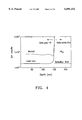
- FIG. 4 is a graph showing the result of the SIMS analysis of the oxygen concentration in the silicon film deposited by the silicon LP-CVD apparatus of the present invention provided with a load lock chamber and that in the silicon film deposited by a normal silicon LP-CVD apparatus.
- FIG. 5 is a graph showing the dependency of the sheet resistance on the temperature of the second RTA, in the titanium silicide film formed on the silicon film of a first example of the present invention deposited by the silicon LP-CVD apparatus of the present invention provided with a load lock chamber and in the titanium silicide film formed on the silicon film deposited by the normal silicon LP-CVD apparatus of the conventional method.
- FIG. 6A is a cross sectional view schematically showing the titanium silicide film formed by the conventional method, after being annealed at 900° C. for 30 minutes in nitrogen gas ambient.
- FIG. 6B is a cross sectional view schematically showing the titanium silicide film formed in the first example of the present invention, after beilg annealed at 900° C. for 30 minutes in nitrogen gas ambient.
- FIG. 7A is a cross sectional view schematically is showing the agglomeration mechanism in the titanium silicide film formed by the conventional method.
- FIG. 7B is a cross sectional view schematically showing the agglomeration mechanism in the titanium silicide film formed in the first example of the present invention.
- FIG. 8 is graph showing the dependency of the sheet resistance on the gate length of the gate electrode having the titanium silicide film formed in the first example of the present invention and that of the gate electrode having the titanium silicide film formed by the conventional method.
- FIG. 9 shows ID-VD characteristics of an LDD transistor having the titanium silicide film formed in the first example and those of an LDD transistor having the titanium silicide film formed by the conventional method.
- FIGS. 10A through 10D are cross sectional views sequentially showing fabrication steps of a semiconductor device of a second example of the present invention.
- FIGS. 11A and 11B are cross sectional views showing a semiconductor device of a fourth example of the present invention.
- FIGS. 12A through 12E are cross sectional views for explaining a semiconductor device formed by the conventional method.
- FIGS. 13A to 13D are cross sectional views of the wafer in the conventional method and the present invention, respectively, after the first step of the rapid thermal annealing (1st Step RTA) is performed.
- FIGS. 14A to 14I are graphs illustrating the line width dependence of the sheet resistances of the titanium silicide films formed by the present example and the conventional method.
- TiN exists between the crystal grains of the TiSi 2 C54 crystal structure. Therefore, the sheet resistance of TiSi 2 is lower than that in the case where SiO 2 exists between the grains.
- the same low value as that in silicidation of the interconnection (e.g., a gate electrode) with a width larger than the grain size of TiSi 2 is obtainable in silicidation of the interconnection with a width smaller than the grain size.
- the surface free energy between TiSi 2 and TiN is smaller than that between TiSi 2 and SiO 2 . That is, at a temperature equal to or more than the temperature allowing re-crystallization (about 815° C.
- the system works s0 as to be stabilized by lowering the surface free energy.
- the system works so as to decrease the contact area between TiSi 2 and SiO 2 (the surface free energy between TiSi 2 and SiO 2 is far larger than that between TiSi 2 and Si or the like).
- the film starts to agglomerate at lower temperatures in comparison with the case where TiN exists between the grains.
- the film having a crystal structure where TiN exists between the grains is highly heat-resistant and does not agglomerate even when being annealed in the furnace approximately at 900° C. for 30 minutes.
- oxygen is mixed with the reaction products in the following manners: oxygen included in the underlying silicon substrate to react with a titanium metal or in the silicon film, especially oxygen in the gate electrode formed of a poly-crystalline silicon film deposited by a normal LPCVD silicon deposition device (oxygen atoms more than 1 ⁇ 10 18 cm -3 are included in the poly-crystalline silicon film deposited by a normal LPCVD silicon deposition device); oxygen included in the native oxide film existing in the interface between the deposited titanium film and the underlying silicon film or the interface between the deposited titanium film and the silicon substrate and oxygen existing in the deposited titanium metal; oxygen absorbing to the surface of the titanium metal when being open to atmosphere for the first RTA; and oxygen mixed into the atmosphere during the first RTA.
- the oxygen knocked on during the ion implantation for forming the source and drain regions in the step as shown in FIG. 12B gets mixed irrespective of the cleanliness of the instrument or gas to be used, and is the most problematic in the conventional technique.
- the oxide film 406 is indispensable for preventing the contamination at the time of the ion implantation.
- a mask formed of photoresist is necessary for implanting donors and acceptors separately from each other.
- the photoresist is applied to the semiconductor substrate through the oxide film 406, since the photoresist to which a heavy metal is mixed at a high ratio cannot be directly applied thereto.
- mixing of oxygen in the process of reaction of titanium and silicon cannot be prevented.
- Table 1 shows generation enthalpies of TiN, TiO 2 , SiO 2 and TiSi 2 . As is apparent from Table 1, the oxides (TiO 2 and SiO 2 ) are most predominantly produced in the quaternary reaction system of Ti, Si, O and N.
- the first RTA should be performed at the lowest possible temperature (575° C. to 650° C.) so that the titanium silicide film grown in the lateral direction may not cause the short between adjacent interconnection (e.g., between the source and the gate, or between the drain and the gate).
- the first RTA may result in the silicidation reaction in the ternary system of Ti, Si and O even though it is performed in refined nitrogen gas ambient. As a result, oxides are predominantly formed in the grain boundary of TiSi 2 .
- the second RTA should be performed at 800° C.
- the TiSi 2 film (basically having a metastable TiSi 2 C 49 crystal structure after the first RTA at around 600° C.) including oxides TiO 2 and SiO 3 is changed into the stable TiSi 2 C 54 crystal structure.
- the oxide phase which changes into TiSi 2 by the annealing at 800° C. or more is only SiO 2 . Accordingly, only SiO 2 exists in the grain boundary of the TiSi 2 film after the second RTA.
- the titanium silicide film formed by the conventional method has high sheet resistance and deteriorates in heat-resistant properties. Especially, the degree of rise in the sheet resistance becomes considerably high in silicidation of the interconnection with a width smaller than the grain size of TiSi 2 (e.g., a gate electrode).
- the TiSi 2 film including SiO 2 in the above-mentioned grain boundary starts to agglomerate from SiO 2 existing in the grain boundary due to the larger surface free energy difference between TiSi 2 and SiO 2 .
- the titanium silicide film thus agglomerated is divided into parts, and no more serves as low resistance interconnection layer having silicide.
- the sheet resistance rises to the level as high as that in the interconnection without having a silicide film.
- Ti atoms diffuse in silicon in the agglomeration step, the leak current increases due to junction destruction in the source/drain region, while the reliability of the gate oxide film deteriorates in the gate electrode.
- a field oxide film 102, an active region 103 and a gate oxide film 104 are formed on a semiconductor substrate 101.
- the semiconductor substrate 101 has been subject to an IG (Intrinsic Gettering) treatment, whereby a DZ (Denuded Zone) zone is formed thereon.
- the surface region of the substrate has an oxygen concentration of 1 ⁇ 10 18 cm -3 or less.
- a poly-crystalline silicon film 105 having a thickness of approximately 1500 ⁇ is deposited by using a silicon LP-CVD (Low Pressure Chemical Vapor Deposition) apparatus provided with a pre-evacuation chamber and a load lock chamber purged by using nitrogen and maintained at a dew point of -100° C. or less (see FIG. 3).
- the deposited film is patterned into a gate electrode, and side wall spacers 106 are formed on the side walls of the gate electrode.
- the method for forming the poly-crystalline silicon film 105 by using the apparatus shown in FIG. 3 is described hereinafter.
- a wafer immediately after undergoing the gate oxidation is put into the pre-evacuation chamber, and the pressure of the pre-evacuation chamber is reduced to be about 10 -1 Pa.
- the wafer is sent to the load lock chamber purged by using nitrogen and maintained at a dew point of -100° C. or less.
- H 2 O molecules absorbed on the surface of the wafer are removed by the purge using nitrogen, the wafer is sent to the furnace where a poly-crystalline silicon film is formed by an LPCVD method at a pressure of 30 Pa, at a temperature about 620° C. in SiH 4 of a degree of purity of 99.9999% or more.
- the concentration of oxygen of the thus formed film is very low, and is equal to or lower than the detection limit (1 ⁇ 10 16 cm -3 ) according to SIMS (Secondary Ion mass Spectrometry) analysis.
- SIMS Secondary Ion mass Spectrometry
- a titanium silicide film 109 having a stoichiometrically metastable TiSi 2 C49 is crystal structure is formed on the gate electrode 105 and the active region 103 in a self-alignment manner.
- This is performed by using a cluster type apparatus having a load lock chamber, an etching chamber, a sputtering chamber, an RTA (Rapid Thermal Annealing) chamber and vacuum conveyer chambers for connecting one chamber to another.
- the wafer is put into the load lock chamber immediately after the native oxide film on the surface of the silicon film (silicon substrate) is removed by using a hydrofluoric acid type solution, and then is conveyed to the etching chamber.
- an argon sputtering cleaning etching method is employed in the present example.
- the oxide film may be removed by reduction removal, which is realized by providing a hydrogen anneal chamber in place of the etching chamber.
- the surface of the substrate is not damaged unlike the method of etching the oxide film by physically sputtering argon atoms. Also, there is another method for removing the oxide film, which is realized by providing an HF gas phase cleaning chamber in place of the etching chamber.
- the wafer is conveyed into the sputtering chamber in a vacuum (1 ⁇ 10 -8 Torr in the present example), where a titanium nitride film 108 of a film thickness about 50 nm is deposited by a reactive sputtering method in a mixture gas of an argon gas and a nitrogen gas at the ratio of nitrogen gas in the range of 0.1% to 10%.
- the wafer is conveyed into the RTA chamber in a vacuum (1 ⁇ 10 -8 Torr in the present example) to be subject to a first RTA for about 20 seconds at temperatures in the range of 575° C. to 650° C. (625° C. in the present example) in nitrogen gas ambient, whereby a titanium silicide film 109 having a TiSi 2 C49 crystal structure is formed on the silicon (103 and 105) due to reaction of titanium and silicon, while the surface region of the deposited titanium nitride film is changed into a titanium nitride film 110 with a higher is nitrogen content.
- a titanium silicide film is not formed in the region where the silicon film (silicon substrate) is not contact with the titanium silicide film 109 (i.e., the region where the gate electrode side wall spacer 106, the field oxide film 102 and the like are placed) since no silicon is supplied therein.
- the titanium silicide film 109 is formed in a self alignment manner only in the regions 103 and 105.
- the titanium silicide film formed in the present example has superior heat resistant properties, since TiN exists in the grain boundaries of the film.
- impurity ions to serve as donors or acceptors in silicon are implanted through the titanium nitride film 110 into the titanium silicide film 109 by an ion implantation method. Due to the activation annealing described later, the region where the ions are implanted becomes source/drain regions 111.
- implantation energy is set so as to satisfy the relationship of T TiSi2 ⁇ Rp+ ⁇ Rp ⁇ T TiSi2 +T TiN where Rp stands for the projected range, ⁇ Rp stands for a standard deviation, T TiSi 2 stands for a thickness of TiSi 2 and T TiN stands for a thickness of TiN.
- 75 As + and 11 B - are implanted as donors and acceptors, respectively, at a dose of 5 ⁇ 10 15 cm -2 . At the same time, they are also implanted into the gate electrode. A transistor of a surface channel type is formed since ions of the same conductivity type as those implanted in the source/drain regions are implanted into the gate electrode.
- the titanium nitride films 108 and 110 are removed by selective etching using a mixture solution of a sulfuric acid and a hydrogen peroxide solution from the surface of the titanium silicide film 109, the field oxide film 102 and the gate electrode side wall spacer 106.
- a second RTA at a temperature of about 800° C. to 1100° C. is performed so as to form a titanium silicide film 112 having a stoichiometrically stable TiSi 2 C54 crystal structure.
- a furnace annealing step which will be described later is performed for the reflow of the interlevel insulator on the titanium silicide film.
- the activation annealing of the donors or the acceptors can be simultaneously performed by the furnace annealing step described later.
- the second RTA is performed at 900° C. for about 20 seconds in N 2 gas.
- the second RTA may be performed at a temperature of 1000° C. to 1100° C. also for the activation annealing of the donors or the acceptors.
- the silicide film in the present example is formed by silicidation reaction from which oxygen is excluded, and TiN exists in the grain boundaries of the formed silicide film.
- the silicide film of the present example has heat-resistant properties superior to those obtained by the conventional method. As shown in FIG. 5, the rise in the sheet resistance due to the agglomeration can be eliminated in the RTA at about 1100° C. for approximately 20 seconds.
- an interlevel insulator 113 is deposited, and furnace annealing is performed for about 10 minutes at 900° C. in N 2 gas both for making the upper face of the interlevel insulator as flat as possible (reflow) and for the activation annealing of implanted impurities.
- furnace annealing is performed for about 10 minutes at 900° C. in N 2 gas both for making the upper face of the interlevel insulator as flat as possible (reflow) and for the activation annealing of implanted impurities.
- a desired semiconductor device is fabricated through a contact formation step and a metallization step (not shown).
- FIG. 6 is a cross sectional view based on TEN (transmission electron microscope) photographs, showing the shape of the titanium silicide film of the present example and that of the conventional method, after being annealed at 900° C. in N 2 gas for 30 minutes. It revealed that the silicide film of the present example, subject to the annealing at 900° C. in N 2 for about 30 minutes, did not agglomerate.
- the titanium silicide film formed by the present example has superior heat-resistant properties. This phenomenon will be described by using a model shown in FIG. 7.
- the surface free energy between TiSi 2 and TiN is smaller than that between TiSi 2 and SiO 2 . Namely, at temperatures higher than the re-crystallization point (about 815° C. in TiSi 2 ), the system works so as to lower the surface free energy for obtaining a more stable state. In this case, the system works so as to reduce the contact area between TiSi 2 and SiO 2 since the surface free energy between TiSi 2 and Si is small.
- the surface free energy between TiSi 2 and TiN is smaller than that between TiSi 2 and SiO 2 .
- agglomeration starts at a lower temperature in the film in which SiO 2 exists between TiSi 2 C54 crystal grains, in comparison with the film in which TiN exists between crystal grains.
- the film in which TiN exists between crystal grains is highly heat-resistant and does not agglomerate even if being subject to the furnace annealing at 900° C. for about 30 minutes.
- FIG. 8 shows the dependency of the sheet resistance on the gate length in the gate electrode having the titanium silicide film formed in the present example and that in the gate electrode having the titanium silicide film formed by the conventional method. It was confirmed that the interconnection sheet resistance did not rise at the gate length of 0.2 ⁇ m or more in both of n + and p - gate electrodes. In addition, it was confirmed that the value of the sheet resistance was far lower than that of the conventional method.
- FIG. 9 and Table 2 show the characteristics of an LDD transistor having the titanium silicide film of the first example in the source/drain and gate regions and those of an LDD transistor having the titanium silicide film formed by the conventional method shown in FIG. 12 in the source/drain and gate regions.
- the film thickness of the gate oxide film is about 5 nm
- the film thickness of the gate electrode side wall spacer is about 100 nm
- the gate length is about 0.26 ⁇ m both for the conventional method and the present invention.
- FIG. 9 shows ID-VD characteristics Of the LDD transistor having the titanium silicide film of the present example and those of the LDD transistor having the titanium silicide film formed by the conventional method. It was confirmed that the current drivability (mutual conductance) of the present invention was improved proved by 50% in comparison with that of the conventional method.
- Table 2 shows the trans-conductance (gml) in the linear region, the trans-conductance (gms) in the saturation region, and the transistor series resistance having the titanium silicide film of the present example and having the titanium silicide film formed by the conventional method.
- the trans-conductance in the linear region and the trans-conductance in the saturation region are improved by about 45% in comparison with those of the conventional method.
- the series resistance is reduced to half or less.
- FIGS. 10A to 10D are cross sectional views showing the fabrication steps of the present invention.
- a field oxide film 202, an active region 203, a gate oxide film 204, a gate electrode 205 and a side wall spacer 206 are formed on a semiconductor substrate 201 having been subject to an IG treatment, in the same manner as that for the process until the step shown in FIG. 1B of the first example. Then, the wafer is put in the load lock chamber of the cluster type apparatus used in the first example, immediately after the native oxide film on the surface of the silicon films 201 and 205 is removed by using a hydrofluoric type solution as shown in FIG. 10A.
- the wafer is conveyed into the etching chamber, and a native oxide film 207 and the like, formed again before the wafer is put in the load lock chamber, are removed again for cleaning the surface of the wafer.
- a native oxide film 207 and the like formed again before the wafer is put in the load lock chamber, are removed again for cleaning the surface of the wafer.
- an argon sputtering cleaning etching method is employed in the present example.
- the oxide film may be removed by reduction removal, which is realized by providing a hydrogen anneal chamber in place of the etching chamber.
- the surface of the substrate is not damaged unlike the method of etching the oxide film by physically sputtering argon atoms.
- there is another method for removing the oxide film which is realized by providing a HF gas phase cleaning chamber in place of the etching chamber.
- the wafer is conveyed into the sputtering chamber in a vacuum (1 ⁇ 10 -8 Torr in the second example), where a titanium nitride film 208 is deposited by a reactive sputtering method in a mixture gas of an argon gas and a nitrogen gas at the ratio of nitrogen gas in the range of 0.1% to 10% (nitrogen gas of 1%, in the second example).
- the wafer is taken out of the cluster apparatus, and silicon ions are implanted.
- the silicon ions are implanted at a dose of 5 ⁇ 10 15 cm -2 . Due to this silicon ion implantation, a layer 209 in which titanium (i.e., titanium containing nitrogen) and silicon are mixed with each other is formed in the interface between the titanium nitride film 208 and the silicon (203 and 205).
- the surface morphology of the titanium nitride film becomes very smooth after the RTA step which will be described later.
- the wafer is once exposed to atmosphere after the deposition of the titanium nitride film.
- This is preferably performed in the cluster type apparatus in which the sputtering chamber and the ion implantation chamber are connected via the vacuum conveyance system.
- a first RTA for about 20 seconds is performed at a temperature in the range of 575° C. to 650° C. (625° C. in the second example) in nitrogen gas ambient, whereby a titanium silicide film 210 having a TiSi 2 C49 crystal structure which is stoichiometrically metastable is formed on the silicon (203 and 205) due to reaction of titanium and silicon, while the surface region of the deposited titanium nitride film is changed into a titanium nitride film 210 with a higher nitrogen content.
- a titanium silicide film is not formed in the region where the silicon film (silicon substrate) is not contact with the titanium silicide film 210 (i.e., the region where the gate electrode side wall spacer 206, the field oxide film 202 and the like are placed), since no silicon is supplied therein.
- the titanium silicide film 210 is formed in a self alignment manner only in the regions (203 and 205).
- TiN exists in the grain boundary, and the surface morphology is very smooth.
- the thus formed titanium silicide film has superior heat resistant properties.
- the gate electrode is obtained by depositing a poly-crystalline silicon film and patterning it.
- the gate electrode may be formed of an amorphous silicon film in place of the poly-crystalline silicon film.
- a silicon LP-CVD apparatus having a pre-evacuation chamber and a load lock chamber purged by using nitrogen and maintained at a dew point of -100° C. or less.
- the semiconductor wafer immediately after the formation of the gate oxide film is conveyed into the pre-evacuation chamber, and the pressure of the pre-evacuation chamber is reduced to be about 10 -1 Pa.
- the wafer is sent to the load lock chamber purged by using nitrogen and maintained at a dew point of -100° C. or less.
- the wafer is sent to the furnace where an amorphous silicon film of about 1500 ⁇ is formed by an LPCVD method at a pressure of 50 Pa and a temperature about 550° C. in the ambient of SiH 4 of a degree of purity of 99.9999% or more.
- the concentration of oxygen of the thus formed film is very low, which is 1 ⁇ 10 18 cm -3 or less.
- a semiconductor device is fabricated through the process steps similar to those of the first and second examples.
- a two-layered film in which an amorphous silicon film is deposited on the poly-crystalline silicon film may be used as the gate electrode.
- the two-layered film may be formed in the following manner.
- a poly-crystalline silicon film is deposited to the thickness of 1000 ⁇ by the method (process sequence) of the first example. Then, the sequence is continuously changed into the conditions for depositing an amorphous silicon film without exposing the wafer to atmosphere, so as to deposit amorphous silicon having a thickness of about 500 ⁇ .
- the oxygen concentration of the thus formed two-layer film is very low, which is 1 ⁇ 10 18 cm -3 or less.
- An amorphous silicon film has no grain boundary as existing in the poly-crystalline silicon film.
- the film to react with the titanium nitride film is an amorphous silicon film, a titanium silicide film having an excellent surface morphology can be formed.
- the present invention is not limited to the silicide transistor having a normal structure, which has been described in the first through third examples.
- an implantation region with a low level of ion concentration may be formed for the LDD transistor by using the gate electrode as a mask.
- phosphorous ions are implanted at a dose of about 3 ⁇ 10 13 cm 2 .
- arsenic ions may be implanted in place of phosphorous ions at a dose amount of about 1 ⁇ 10 14 cm 2 for the purpose of local extended Junction. (Our experiment revealed that there was little influence of knocked on oxygen on the silicidation reaction in the arsenic ion implantation at an order of the 14th power).
- the present invention can also be applied to the transistor of the type having a stacked diffusion layer as shown in FIGS. 11A and 11B.
- a field oxide film 302 an active region 303, a gate oxide film 304, a gate electrode 305 and a side wall spacer 306 are formed on a semiconductor substrate 301.
- the gate electrode 305 is formed of a poly-crystalline silicon film, an amorphous silicon film or a two-layered film composed of a poly-crystalline silicon film and an amorphous silicon film such that the oxygen concentration becomes 1 ⁇ 10 18 cm -3 or less, in the manner similar to that of the first through third examples.
- a single-crystalline silicon film or a non-single-crystalline silicon film such that the oxygen concentration becomes 1 ⁇ 10 18 cm -3 or less is selectively grown on the active region so as to grow a stacked silicon region 307.
- a technique for conducting the selective growth includes following methods:
- a method using a silicon LP-CVD apparatus described in the first through third examples of the present invention having a pre-evacuation chamber and a load lock chamber purged by using nitrogen and maintained at a dew point of -100° C. or less, in which an epitaxial growth in accordance with the crystal orientation of an underlying crystal substrate is performed in the active region, while a film such that it causes a poly-crystalline silicon film (in the case of film formation at 590° C. or more) or an amorphous silicon film (in the case of film formation at 590° C. or less) to be deposited is deposited in the region where the silicon substrate is not exposed, and then the poly-crystalline silicon film or the amorphous silicon film is removed by selective etching so as to selectively grow a silicon film on the active region;
- a method using the above-mentioned silicon LP-CVD apparatus in which an epitaxial growth in accordance with the crystal orientation of an underlying crystal substrate is performed in the active region, while, in the region where the silicon substrate is not exposed, a film such that it causes a poly-crystalline silicon film or an amorphous silicon film is deposited, or a poly-crystalline silicon film or an amorphous silicon film is deposited over the entire face of the wafer, and thereafter the poly-crystalline silicon film or the amorphous silicon film is polished by a chemical and mechanical polishing method until the top of the gate electrode is exposed, and then is patterned in the field region.
- the gate electrode and source/drain regions 309 both having titanium silicide films as backing layers are formed by the method of the first or second example.
- the source/drain regions are grown to be higher than the gate channel region. This makes the transistor less affected by the short channel effects.
- the present invention oxygen is excluded in the silicidation reaction, and a titanium silicide film is formed by causing a titanium nitride film instead of a Ti metal to react with silicon.
- TiN in place of SiO 2 exists in the grain boundaries of the TiSi 2 .
- the sheet resistance of the thus formed TiSi 2 film is low.
- the interconnection resistivity in silicidation of the interconnection with a width less than the grain size of the TiSi 2 film is not far larger than in silicidation of the interconnection with a width more than the grain size of the TiSi 2 film.
- the same low value as that obtained in silicidation of the interconnection with a width larger than the grain size is advantageously obtainable in silicidation of the interconnection with a width less than the grain size of the TiSi 2 film.
- the film is advantageously free from the agglomeration even if the annealing for activation of implanted donors or acceptors or the annealing for the reflow of the interlevel insulator is performed in the furnace annealing at 900° C. and for approximately 30 minutes after the silicide film formation.
- the impurities are implanted after the silicide film formation, the damage due to the implantation scarcely reach the silicon film (silicon substrate) below the silicide film.
- the damage due to the implantation scarcely reach the silicon film (silicon substrate) below the silicide film.
- Example 5 A silicidation reaction performed in a system where oxygen is removed as much as possible is illustrated in the following as Example 5.
- the oxygen concentration in the surface region of the semiconductor substrate which becomes the source/drain region is kept at or below 1 ⁇ 10 18 cm -3 by performing IG treatment and by forming the DZ zone.
- the oxygen concentration in the poly-crystalline silicon film which becomes the gate electrode is kept at an extremely low level by depositing the film using the above-mentioned silicon LPCVD deposition device including the load lock chamber (FIG. 4).
- an oxide film is natively formed on the surface of the poly-crystalline silicon film (silicon substrate) at the moment when surface is exposed to an atmosphere. That is, even though the surface of the poly-crystalline silicon film (silicon substrate) is cleaned (the cleaning process including the removal of the oxide film by etching) with a hydrofluoric acid-based solution before depositing a titanium (titanium nitride) film for silicidation, if the wafer is carried through an atmosphere to the device for depositing titanium (titanium nitride), a new native oxide film is formed on the surface of the poly-crystalline film (silicon substrate), thereby creating a situation where oxygen (the oxide film) exists at the interface between the titanium (titanium nitride) film to be deposited in the next step and the poly-crystalline silicon film (silicon substrate).
- a titanium (titanium nitride) film is deposited in a cluster-type apparatus including a load look chamber, an etching chamber, a sputtering chamber and a rapid thermal annealing (RTA) chamber, which are all connected by vacuum conveyers.
- a cluster-type apparatus including a load look chamber, an etching chamber, a sputtering chamber and a rapid thermal annealing (RTA) chamber, which are all connected by vacuum conveyers.
- the titanium silicide film is formed in the cluster-type apparatus as follows. First, a wafer, immediately after the removal of the native oxide film from the wafer surface by a hydrofluoric acid-based solution, is placed inside the load lock chamber. Then, the wafer is conveyed to the etching chamber where the native oxide film formed during the time interval between the removal of initially formed native oxide film on the wafer surface and its placement in the load lock chamber is removed by a hydrofluoric acid-based solution, thereby cleaning the wafer surface. Then, a titanium (titanium nitride) film is deposited in an argon ambient by sputtering, after which the silicidation reaction takes place.
- the method of cleaning the wafer is to perform a chemical plasma etching by a fluorine-based gas such as CF 4 , C 4 F 8 , NF 3 , etc. added with a reducing gas such as H 2 O/H 2 , etc., thereby removing the oxide film.
- a fluorine-based gas such as CF 4 , C 4 F 8 , NF 3 , etc.
- a reducing gas such as H 2 O/H 2 , etc.
- the native oxide film is removed in-a wet washing chamber (a native oxide film removing chamber using a hydrofluoric acid-based solution) which is connected to the cluster-type apparatus via the load lock chamber and whose environment is controlled under the inert gas environment or the nitrogen gas environment. Then, without exposing the wafer to an atmosphere, the wafer is conveyed to the load lock chamber and, after vacuum is drawn, to the sputtering chamber where the titanium (titanium nitride) film is deposited.
- a wet washing chamber a native oxide film removing chamber using a hydrofluoric acid-based solution
- the important point in the silicidation reaction is that the oxygen concentration in the region where the silicidation reaction takes place is 1 ⁇ 10 18 cm -' or less, thereby improving both the sheet resistance and the heat-resistance substantially.
- the native oxide film on the surface of the poly-crystalline silicon film (silicon substrate) is removed, and then, instead of depositing a TiN film which is rich in titanium in the previous examples, a pure titanium film is deposited by the above-mentioned method. Then, the silicidation reaction is initiated by the two-step rapid thermal annealing (2-step RTA) as in the previous examples.
- FIG. 13A is a cross sectional view illustrating the wafer after depositing a poly-crystalline silicon film 605 (to become a gate electrode), then removing the native oxide film by treating it with hydrofluoric acid, then exposing it to and conveying it through an atmosphere, and then depositing a titanium film 511 in the titanium sputtering chamber in accordance with the conventional method.
- FIG. 13B is a cross sectional view of the wafer after depositing the titanium film 511 in accordance with the method of the present example.
- the oxygen concentration within the poly-crystalline silicon film 605 is high (at 1 ⁇ 10 19 cm -3 or more) as illustrated in FIG. 4. Furthermore, since the wafer is carried to the sputtering chamber while being exposed to an atmosphere, the surface of the poly-crystalline silicon film is oxidized (or water molecules present in the atmosphere adhere to the surface) and a native oxide film 510 is formed at the interface between the titanium film 511 and the poly-crystalline film 605.
- the oxygen concentration within the poly-crystalline silicon film 505 is below the detection threshold (at 1 ⁇ 10 18 cm -3 or less; see FIG. 4). Moreover, since the titanium film 511 is deposited after the native oxide film formed on the surface of the poly-crystalline silicon film is removed in the above-described cluster-type apparatus, it is possible to keep the oxygen concentration in the silicidation reaction system at 1 ⁇ 10 18 cm -3 or less as a total.
- the reaction system of poly-crystalline silicon to become a gate electrode
- titanium the same is true for the native oxide film at the interface between the silicon substrate and the titanium film in the reaction system of the silicon semiconductor substrate (to become a source/drain region) and the titanium.
- the oxygen concentration within the silicon substrate is typically about 2 ⁇ 10 18 to 5 ⁇ 10 18 cm -3 , it is necessary to form a substantially oxygenless and substantially defect free layer on the substrate surface by performing the IG treatment so that the oxygen concentration in the region to react with titanium is reduced.
- FIGS. 13A to 13D are cross sectional views of the wafer in the conventional method and the present example, respectively, after the first step of the rapid thermal annealing (1st Step RTA) is performed.
- the rapid thermal annealing in the present example is performed at 675° C. in the nitrogen environment for 10 seconds.
- the silicidation reaction proceeds while the titanium reduces the native oxide film.
- a nitridation reaction also takes place.
- the titanium silicide film 513 of the C49 crystal structure containing a large amount of oxygen and the titanium nitride film 512 created by nitridation reaction are formed.
- the silicidation reaction proceeds while reducing the oxygen, the silicidation reaction does not uniformly proceed and the Interface between the silicon film 605 and the titanium silicide film 513 becomes uneven.
- the titanium silicide film is uniformly formed and the interface between the silicon film 505 and the titanium silicide film 514 becomes even. Furthermore, because the silicidation reaction takes place within a nitrogen environment, the nitrogen diffuses as far as to the silicide film during the silicidation reaction, thereby creating a titanium silicide film containing the nitrogen.
- the titanium silicide film in the conventional example contains nitrogen in addition to oxygen, the large amount of oxygen contained is the problem. In particular, oxygen is likely to precipitate at the grain boundary, and the situation illustrated in FIG. 7A is ultimately realized.
- titanium instead of titanium nitride was deposited and the result was compared to that of the conventional example. Because the first step of the RTA is performed in the nitrogen environment, the nitrogen precipitates at the grain boundary and a structure similar to that in the previous example illustrated in FIG. 7B is obtained. In order to actively form TiN at the grain boundary in the titanium silicide, a titanium nitride film which is rich in titanium is deposited instead of a titanium film, and then the silicidation reaction is initiated as in the previous example.
- the titanium film is formed on the silicon substrate and then annealed to form the TiSi 2 C49 film. While this is occurring, the upper and lower portions of the Ti film becomes TiN and TiSi 2 , respectively. Although there may be a portion of the Ti film remaining unchanged, this does not pose a problem. However, the Ti film is typically formed in accordance with the desired film thickness of the TiSi 2 film.
- the process for removing the oxygen is not limited to those described in the present example. What is important is keeping the oxygen concentration of the system at a low level with respect to the total reaction system where silicon and titanium are reacted to form a titanium silicide film.
- FIGS. 14A to 14I Illustrated in FIGS. 14A to 14I are the line width dependence of the sheet resistances of a titanium silicide film and a polyside gate electrode formed by the present example and by the conventional method.
- the titanium silicide films and the polyside gate electrodes according to the present example are formed by a reaction between titanium (not titanium nitride) and silicon, and between titanium and poly-crystalline silicon, respectively, within a system which substantially excludes oxygen.
- the titanium silicide films and the polyside gate electrodes according to the conventional method are formed by a reaction between titanium and silicon, and between titanium and poly-crystalline silicon, respectively, within a system including oxygen.
- the titanium silicide film containing oxygen in the conventional example requires a high temperature heat treatment to make the phase transition take place from C49 (high resistance) to C54 (low resistance).
- the phase transition from C49 to C54 is inhibited by the exhistence of oxygen.
- the line width becomes smaller, the resistance rises.
- the reason is as follows. As illustrated in FIG. 7A, due to the precipitation of oxygen at the grain boundary, a high resistance oxide film is formed. As the lines become finer, the structure becomes a bamboo structure, thereby blocking the current path with the oxide film and therefore raising the resistance. Moreover, in the conventional example, as the line width becomes small, the heat-resistance becomes degraded and the resistance rises. At the line width of 0.6 ⁇ m or less, the temperature at which the agglomeration begins is lower than the temperature at which the phase transition to the low resistance C54 crystal structure takes place.
- the resistance does not decrease due to the phase transition but rather increases due to the agglomeration. This phenomena primarily attributable to the bamboo structure under the fine wiring.
- the poor heat-resistance and the agglomeration due to the migration resulting from the large surface free energy also contribute, thereby severing the silicide film.
- the sheet resistance after the second RTA performed at 1000° C. exceeds 100 ⁇ .
- the silicide film has already completely been agglomerated and isolated in stripe configuration, and the sheet resistance thereof has become the sheet resistance of the poly-crystalline silicon film (the silicide film is severed and does not contribute to the gate sheet resistance).
- the phase transition from C49 (high resistance) to C54 (low resistance) occurs at low temperature (and therefore is likely to make the phase transition).
- the heat-resistance is excellent and no increase at all in sheet resistance occurs even after the second RTA performed at 1000° C. is observed.
- the sheet resistance does not depend on the line width and keeps the low resistance down to fine wiring.
Abstract
A method for fabricating a semiconductor device of the invention, the method includes the steps of: providing an oxygen concentration in a region of a silicon film of 1×1018 cm-3 or less; depositing a film including a metal on the silicon film; and reacting the silicon film with the film including a metal so as to form a metal silicide film in the region of the silicon film.
Description
This application is a continuation of Ser. No. 08/736,907 Oct. 25, 1996 U.S. Pat. No. 5,849,634 which is CIP of Ser. No. 08/423,585 Apr. 14, 1995 abandoned.
1. Field of the Invention
The present invention relates to a method for fabricating a semiconductor device, more particularly to a method for fabricating a low resistance titanium silicide film providing good heat-resistant properties.
2. Description of the Related Art
A conventional self-aligned- and silicidation method is described with reference to FIG. 12. First, a field oxide film 402, a gate oxide film 403 and a gate electrode 404 made of poly-crystalline silicon and having side walls covered with an insulating film 405 are formed on a semiconductor substrate 401 as shown in FIG. 12A. Then, as shown in FIG. 12B, after forming an oxide film 406, a high concentration of impurity ions are implanted through the oxide film 406 into the portions to be source/drain regions. Arsenic ions are implanted in the case of NMOS, while boron ions are implanted in the case of PMOS. Thereafter, annealing for activation is performed (e.g., in nitrogen gas ambient, at 900° C. for 10 minutes) so as to form source/drain regions 407. Next, as shown in FIG. 12C, the oxide film 406 over the source/drain regions 407 end the gate electrode 404 is removed by using a solution containing hydrofluoric acid or the like, and thereafter a titanium metal film 408 is deposited by sputtering in argon gas ambient. Then, as shown in FIG. 12D, first RTA (Rapid Thermal Annealing) is performed for about 20 seconds at 650° in nitrogen gas ambient, so as to make silicon and a titanium metal in the source/drain regions 407 and the gate electrode 404 react with each other, thereby forming titanium silicide films 409 each having a TiSi2 C 49 crystal structure which is stoichiometrically metastable (herein, the surface of the titanium metal film 408 changes into a titanium nitride film 410). Then, as shown in FIG. 12E, an unreacted titanium metal film 408 and the titanium nitride film 410 formed by the first RTA are removed by selective etching by using a mixed solution of sulfuric acid and a hydrogen peroxide solution. Thereafter, second RTA is performed at 800° C. for about 20 seconds in nitrogen gas ambient so as to change the titanium silicide film 409 into a titanium silicide film 411 having a TiSi2 C 54 crystal structure which is, stoichiometrically stable.
In the method for fabricating a semiconductor device, after the step of forming transistors, an interlevel insulator is deposited on the transistor. Then, an annealing step for densifying and reflowing the interlevel insulator is performed. Normally, the annealing step is effective at 850° C. or more, and preferably at 900° or more.
However, the conventional process for forming a titanium silicide film has the following problems:
(1) The inclusion of oxygen resulting from process steps (e.g., a step of implanting impurity ions through the oxide film) cannot be prevented in the system of reaction of Ti and Si, no matter how the cleanliness of the instrument and surrounding conditions for the fabrication are improved. As a result, the silicidation reaction occurs in the ternary system of Ti, Si and O.
(2) In the silicidation reaction in the ternary system, SiO2 is predominantly formed in the grain boundary of TiSi2, which makes the sheet resistance higher and results in deterioration of heat resistance. This problem is prominent especially in silicidation for interconnection with a width less than the grain size of TiSi2. That is, in silicidation of the interconnection with a width less than the grain size of TiSi2, the change in crystal structure from C49 to C 54 is hard to occur in RTA at 900° C. or less. As a result, a titanium silicide film having extremely high electrical resistance (sheet resistance) is obtained. In the case of performing the RTA at a temperature of 900° C. or more, the change in crystal structure from C49 to C 54 is likely to occur. However, heat resistance deterioration and agglomeration of the silicide film are likely to occur in comparison with the silicide film obtained by silicidation of the interconnection with a large width. In addition, since the agglomeration of the silicide film starts also in the silicide film with a further large width, the agglomeration is inevitable.
(4) In the case where the silicide film is formed by the conventional silicidation method and then annealing at a temperature of more than 800° C. is performed for the reflow of the interlevel insulator, the agglomeration occurs and the junction leakage of the source and drain regions increases, whereas the reliability of the gate oxide film deteriorates. In addition, the interconnection resistance rises, and especially, in the case of the silicidation of the interconnection (e.g., a gate electrode) with a width smaller than the grain size of TiSi2, the sheet resistance rises to the level as high as the level in the interconnection not having a silicide film.
A method for fabricating a semiconductor device of this invention, the method includes the steps of: providing an oxygen concentration in a region of a silicon film of 1×1018 cm-3 or less; depositing a film including a metal on the silicon film; and reacting the silicon film with the film including a metal so as to form a metal silicide film in the region of the silicon film.
In one embodiment of the invention, the film including a metal comprises a titanium film, and the metal silicide film comprises a titanium silicide film.
In another embodiment of the invention, the film including a metal comprises a titanium nitride film in which titanium atoms are more than nitride atoms, and the metal silicide film comprises a titanium silicide film.
In still another embodiment of the invention, the method further includes the step of forming the titanium silicide film including TiSi2 C54 crystal grains which are in contact with each other via TiN.
In yet another embodiment of the invention, the method further includes the step of forming the titanium silicide film including TiSi2 C54 crystal grains which are in contact with each other via TiN.
In yet another embodiment of the invention, the method further includes the step of: implanting silicon ions in the vicinity of an interface between the titanium film and the silicon film, after depositing the titanium film and before reacting the silicon film with the titanium film.
In yet another embodiment of the invention, the method further includes the step of: implanting silicon ions in the vicinity of an interface between the titanium nitride film and the silicon film, after depositing the titanium nitride film and before reacting the silicon film with the titanium nitride film.
In yet another embodiment of the invention, the titanium nitride film is deposited by a reactive sputtering method using a titanium target in a mixture gas of an argon gas and a nitrogen gas, the mixing ratio of the nitrogen gas in the mixture gas being in the range of 0.1% to 10%.
In yet another embodiment of the invention, the method further includes the steps of: removing a native oxide film on the silicon film and then depositing the titanium film on the silicon film without being open to atmosphere; performing E first rapid thermal annealing in a nitrogen gas and making the titanium film and the silicon film react with each other so as to form a titanium silicide film having a TiSi2 C49 crystal structure which is stoichiometrically metastable, and form a titanium nitride film in the surface region of the titanium film above the titanium silicide film; implanting impurities serving as donors or acceptors into the titanium silicide film and the silicon film beneath the titanium silicide film by an ion implantation method, said implanting being performed through the titanium nitride film above the titanium silicide film; selectively removing the titanium nitride film above the titanium silicide film and the titanium nitride film located in a region where the titanium silicide film is not formed; and changing the titanium silicide film into a TiSi2 C54 crystal structure which is stoichiometrically stable by a second rapid thermal annealing.
In yet another embodiment of the invention, the method further includes the steps of: removing a native oxide film on the silicon film and then depositing the titanium nitride film on the silicon film without being exposed to atmosphere; performing a first rapid thermal annealing in a nitrogen gas thereby causing the titanium nitride film and the silicon film to react with each other so as to form a titanium silicide film having a TiSi2 C49 crystal structure which is stoichiometrically metastable, and form a titanium nitride film in the surface region of the titanium nitride film above the titanium silicide film; implanting impurities serving as donors or acceptors into the titanium silicide film and the silicon film beneath the titanium silicide film by an ion implantation method, said implanting being performed through the titanium nitride film above the titanium silicide film; selectively removing the titanium nitride film above the titanium silicide film and the titanium nitride film located in a region where the titanium silicide film is not formed; and changing the titanium silicide film into a TiSi2 C54 crystal structure which is stoichiometrically stable by a second rapid thermal annealing.
In yet another embodiment of the invention, the method further includes the step of: implanting silicon ions in the vicinity of an interface between the titanium film and the silicon film, said implanting of silicon ions being performed after depositing the titanium film and before the first rapid thermal annealing.
In yet another embodiment of the invention, the method further includes the step of: implanting silicon ions in the vicinity of an interface between the titanium nitride film and the silicon film, said implanting of silicon ions being performed after depositing the titanium nitride film and before the first rapid thermal annealing.
In yet another embodiment of the invention, the method further includes the step of providing an oxygen concentration in a total region including the region of the silicon film, a region of the film including a metal corresponding to the region of the silicon film, and an interface of the silicon film and the film including a metal, in which the titanium silicide film is to be formed is 1×1018 cm-3 or less.
In yet another embodiment of the invention, the metal includes a refractory metal.
In yet another embodiment of the invention, the step of reacting the silicon film with the film including a metal comprises a step of annealing the silicon film and the film including a metal.
Thus, the present invention described herein makes possible the advantages of (1) providing a semiconductor device having low sheet resistance such that, with respect to the sheet resistance of the TiSi2 film, the same low value of as that obtained in silicidation of the interconnection with a width larger than the grain size of TiSi2 is obtainable even in silicidation of the interconnection with a width smaller than the grain size, and so heat-resistant that it does not agglomerate even when being annealed in the furnace approximately at 900° C. for 30 minutes; and (2) providing a method for fabricating such a semiconductor device.
These and other advantages of the present invention will become apparent to those skilled in the art upon reading and understanding the following detailed description with reference to the accompanying drawings.
FIGS. 1A through 1E are cross sectional views sequentially showing fabrication steps of a semiconductor device of a first example of the present invention.
FIGS. 2A through 2C are cross sectional views sequentially showing fabrication steps of the semiconductor device of the first example of the present invention.
FIG. 3 is a schematic diagram showing a silicon LP-CVD apparatus provided with a load lock chamber used in the present example.
FIG. 4 is a graph showing the result of the SIMS analysis of the oxygen concentration in the silicon film deposited by the silicon LP-CVD apparatus of the present invention provided with a load lock chamber and that in the silicon film deposited by a normal silicon LP-CVD apparatus.
FIG. 5 is a graph showing the dependency of the sheet resistance on the temperature of the second RTA, in the titanium silicide film formed on the silicon film of a first example of the present invention deposited by the silicon LP-CVD apparatus of the present invention provided with a load lock chamber and in the titanium silicide film formed on the silicon film deposited by the normal silicon LP-CVD apparatus of the conventional method.
FIG. 6A is a cross sectional view schematically showing the titanium silicide film formed by the conventional method, after being annealed at 900° C. for 30 minutes in nitrogen gas ambient.
FIG. 6B is a cross sectional view schematically showing the titanium silicide film formed in the first example of the present invention, after beilg annealed at 900° C. for 30 minutes in nitrogen gas ambient.
FIG. 7A is a cross sectional view schematically is showing the agglomeration mechanism in the titanium silicide film formed by the conventional method.
FIG. 7B is a cross sectional view schematically showing the agglomeration mechanism in the titanium silicide film formed in the first example of the present invention.
FIG. 8 is graph showing the dependency of the sheet resistance on the gate length of the gate electrode having the titanium silicide film formed in the first example of the present invention and that of the gate electrode having the titanium silicide film formed by the conventional method.
FIG. 9 shows ID-VD characteristics of an LDD transistor having the titanium silicide film formed in the first example and those of an LDD transistor having the titanium silicide film formed by the conventional method.
FIGS. 10A through 10D are cross sectional views sequentially showing fabrication steps of a semiconductor device of a second example of the present invention.
FIGS. 11A and 11B are cross sectional views showing a semiconductor device of a fourth example of the present invention.
FIGS. 12A through 12E are cross sectional views for explaining a semiconductor device formed by the conventional method.
FIGS. 13A to 13D are cross sectional views of the wafer in the conventional method and the present invention, respectively, after the first step of the rapid thermal annealing (1st Step RTA) is performed.
FIGS. 14A to 14I are graphs illustrating the line width dependence of the sheet resistances of the titanium silicide films formed by the present example and the conventional method.
The examples of the present invention will be described hereinafter, with reference to the accompanying. drawings.
In the semiconductor device of the present invention, TiN exists between the crystal grains of the TiSi2 C54 crystal structure. Therefore, the sheet resistance of TiSi2 is lower than that in the case where SiO2 exists between the grains. In particular, with respect to the sheet resistance of the TiSi2 film, the same low value as that in silicidation of the interconnection (e.g., a gate electrode) with a width larger than the grain size of TiSi2 is obtainable in silicidation of the interconnection with a width smaller than the grain size. Furthermore, the surface free energy between TiSi2 and TiN is smaller than that between TiSi2 and SiO2. That is, at a temperature equal to or more than the temperature allowing re-crystallization (about 815° C. in TiSi2), the system works s0 as to be stabilized by lowering the surface free energy. As a result, the system works so as to decrease the contact area between TiSi2 and SiO2 (the surface free energy between TiSi2 and SiO2 is far larger than that between TiSi2 and Si or the like). Accordingly, in the case where SiO2 exists between the grains of TiSi2 C54 crystals, the film starts to agglomerate at lower temperatures in comparison with the case where TiN exists between the grains. Conversely, the film having a crystal structure where TiN exists between the grains is highly heat-resistant and does not agglomerate even when being annealed in the furnace approximately at 900° C. for 30 minutes.
In the reaction of Ti and Si, there is possibility that oxygen is mixed with the reaction products in the following manners: oxygen included in the underlying silicon substrate to react with a titanium metal or in the silicon film, especially oxygen in the gate electrode formed of a poly-crystalline silicon film deposited by a normal LPCVD silicon deposition device (oxygen atoms more than 1×1018 cm-3 are included in the poly-crystalline silicon film deposited by a normal LPCVD silicon deposition device); oxygen included in the native oxide film existing in the interface between the deposited titanium film and the underlying silicon film or the interface between the deposited titanium film and the silicon substrate and oxygen existing in the deposited titanium metal; oxygen absorbing to the surface of the titanium metal when being open to atmosphere for the first RTA; and oxygen mixed into the atmosphere during the first RTA.
Furthermore, the oxygen knocked on during the ion implantation for forming the source and drain regions in the step as shown in FIG. 12B gets mixed irrespective of the cleanliness of the instrument or gas to be used, and is the most problematic in the conventional technique. The oxide film 406 is indispensable for preventing the contamination at the time of the ion implantation. In particular, in the CMOS process, a mask formed of photoresist is necessary for implanting donors and acceptors separately from each other. The photoresist is applied to the semiconductor substrate through the oxide film 406, since the photoresist to which a heavy metal is mixed at a high ratio cannot be directly applied thereto. Thus, in the conventional technique, mixing of oxygen in the process of reaction of titanium and silicon cannot be prevented.
Table 1 shows generation enthalpies of TiN, TiO2, SiO2 and TiSi2. As is apparent from Table 1, the oxides (TiO2 and SiO2) are most predominantly produced in the quaternary reaction system of Ti, Si, O and N.
              TABLE 1
______________________________________
Generation enthalpy of compounds produced among Ti, Si,
O and N
         Generation enthalpy
         (KJ/mol)
______________________________________
TiO.sub.2  -992
SiO.sub.2  -909
TiN        -339
TiSi.sub.2 -134
______________________________________
The first RTA should be performed at the lowest possible temperature (575° C. to 650° C.) so that the titanium silicide film grown in the lateral direction may not cause the short between adjacent interconnection (e.g., between the source and the gate, or between the drain and the gate). In the conventional TiSi2 film forming method, the first RTA may result in the silicidation reaction in the ternary system of Ti, Si and O even though it is performed in refined nitrogen gas ambient. As a result, oxides are predominantly formed in the grain boundary of TiSi2. The second RTA should be performed at 800° C. or more in order that the TiSi2 film (basically having a metastable TiSi2 C 49 crystal structure after the first RTA at around 600° C.) including oxides TiO2 and SiO3 is changed into the stable TiSi2 C 54 crystal structure. In the ternary system of Ti, Si and O, the oxide phase which changes into TiSi2 by the annealing at 800° C. or more is only SiO2. Accordingly, only SiO2 exists in the grain boundary of the TiSi2 film after the second RTA.
The titanium silicide film formed by the conventional method has high sheet resistance and deteriorates in heat-resistant properties. Especially, the degree of rise in the sheet resistance becomes considerably high in silicidation of the interconnection with a width smaller than the grain size of TiSi2 (e.g., a gate electrode). The melting point of TiSi2 (Tm) is 1813K (=1540° C.). Generally, re-crystallization of metals or the like is prominent at a temperature 0.6 time the melting point (Tm) (0.6 Tm=1088K=815° C.). Hence, by the annealing at 850° C. or more as required for the step of the reflow of the interlevel insulator, the TiSi2 film including SiO2 in the above-mentioned grain boundary starts to agglomerate from SiO2 existing in the grain boundary due to the larger surface free energy difference between TiSi2 and SiO2. The titanium silicide film thus agglomerated is divided into parts, and no more serves as low resistance interconnection layer having silicide. Especially, in silicidation of the interconnection layer with a width smaller than the grain size of TiSi2 (e.g., a gate electrode), the sheet resistance rises to the level as high as that in the interconnection without having a silicide film. Furthermore, since Ti atoms diffuse in silicon in the agglomeration step, the leak current increases due to junction destruction in the source/drain region, while the reliability of the gate oxide film deteriorates in the gate electrode.
First, as shown in FIG. 1A, a field oxide film 102, an active region 103 and a gate oxide film 104 are formed on a semiconductor substrate 101. The semiconductor substrate 101 has been subject to an IG (Intrinsic Gettering) treatment, whereby a DZ (Denuded Zone) zone is formed thereon. The surface region of the substrate has an oxygen concentration of 1×1018 cm-3 or less.
Next, as shown in FIG. 1B, a poly-crystalline silicon film 105 having a thickness of approximately 1500 Å is deposited by using a silicon LP-CVD (Low Pressure Chemical Vapor Deposition) apparatus provided with a pre-evacuation chamber and a load lock chamber purged by using nitrogen and maintained at a dew point of -100° C. or less (see FIG. 3). The deposited film is patterned into a gate electrode, and side wall spacers 106 are formed on the side walls of the gate electrode.
The method for forming the poly-crystalline silicon film 105 by using the apparatus shown in FIG. 3 is described hereinafter. First, a wafer immediately after undergoing the gate oxidation is put into the pre-evacuation chamber, and the pressure of the pre-evacuation chamber is reduced to be about 10-1 Pa. The wafer is sent to the load lock chamber purged by using nitrogen and maintained at a dew point of -100° C. or less. After H2 O molecules absorbed on the surface of the wafer are removed by the purge using nitrogen, the wafer is sent to the furnace where a poly-crystalline silicon film is formed by an LPCVD method at a pressure of 30 Pa, at a temperature about 620° C. in SiH4 of a degree of purity of 99.9999% or more. As shown in FIG. 4, the concentration of oxygen of the thus formed film is very low, and is equal to or lower than the detection limit (1×1016 cm-3) according to SIMS (Secondary Ion mass Spectrometry) analysis. In the experiment where the silicide film is formed through the process similar to that of the present example except that the film having a concentration of oxygen of 2×1018 cm-3 is used as the silicon film, a silicide film having heat resistant properties intermediate between the conventional technique and the present invention was obtained.
Next, as shown in FIG. 1C, after the native oxide film on the surface of the wafer is removed by using a hydrofluoric type solution, a titanium silicide film 109 having a stoichiometrically metastable TiSi2 C49 is crystal structure is formed on the gate electrode 105 and the active region 103 in a self-alignment manner. This is performed by using a cluster type apparatus having a load lock chamber, an etching chamber, a sputtering chamber, an RTA (Rapid Thermal Annealing) chamber and vacuum conveyer chambers for connecting one chamber to another.
Hereinafter, the method for forming the titanium silicide film in the cluster type apparatus will be described in detail. First, as shown in FIG. 2A, the wafer is put into the load lock chamber immediately after the native oxide film on the surface of the silicon film (silicon substrate) is removed by using a hydrofluoric acid type solution, and then is conveyed to the etching chamber. A native oxide film 107 and the like, formed again before the wafer is put in the load lock chamber, are removed again for cleaning the surface of the wafer. As a technique for cleaning, an argon sputtering cleaning etching method is employed in the present example. (Alternatively, the oxide film may be removed by reduction removal, which is realized by providing a hydrogen anneal chamber in place of the etching chamber. In this method, the surface of the substrate is not damaged unlike the method of etching the oxide film by physically sputtering argon atoms. Also, there is another method for removing the oxide film, which is realized by providing an HF gas phase cleaning chamber in place of the etching chamber.
Then, as shown in FIG. 2B, the wafer is conveyed into the sputtering chamber in a vacuum (1×10⁻⁸ Torr in the present example), where a titanium nitride film 108 of a film thickness about 50 nm is deposited by a reactive sputtering method in a mixture gas of an argon gas and a nitrogen gas at the ratio of nitrogen gas in the range of 0.1% to 10%.
Next, as shown in FIG. 2C, the wafer is conveyed into the RTA chamber in a vacuum (1×10⁻⁸ Torr in the present example) to be subject to a first RTA for about 20 seconds at temperatures in the range of 575° C. to 650° C. (625° C. in the present example) in nitrogen gas ambient, whereby a titanium silicide film 109 having a TiSi2 C49 crystal structure is formed on the silicon (103 and 105) due to reaction of titanium and silicon, while the surface region of the deposited titanium nitride film is changed into a titanium nitride film 110 with a higher is nitrogen content. Herein, a titanium silicide film is not formed in the region where the silicon film (silicon substrate) is not contact with the titanium silicide film 109 (i.e., the region where the gate electrode side wall spacer 106, the field oxide film 102 and the like are placed) since no silicon is supplied therein. Hence, the titanium silicide film 109 is formed in a self alignment manner only in the regions 103 and 105. Thus, the titanium silicide film formed in the present example has superior heat resistant properties, since TiN exists in the grain boundaries of the film.
Next, as shown in FIG. 1D, impurity ions to serve as donors or acceptors in silicon are implanted through the titanium nitride film 110 into the titanium silicide film 109 by an ion implantation method. Due to the activation annealing described later, the region where the ions are implanted becomes source/drain regions 111. In the present example, implantation energy is set so as to satisfy the relationship of TTiSi2 ≦Rp+ΔRp≦TTiSi2 +TTiN where Rp stands for the projected range, ΔRp stands for a standard deviation, TTiSi 2 stands for a thickness of TiSi2 and TTiN stands for a thickness of TiN. In the present example, 75 As+ and 11 B- are implanted as donors and acceptors, respectively, at a dose of 5×1015 cm-2. At the same time, they are also implanted into the gate electrode. A transistor of a surface channel type is formed since ions of the same conductivity type as those implanted in the source/drain regions are implanted into the gate electrode.
Next, the titanium nitride films 108 and 110 are removed by selective etching using a mixture solution of a sulfuric acid and a hydrogen peroxide solution from the surface of the titanium silicide film 109, the field oxide film 102 and the gate electrode side wall spacer 106. Thereafter, a second RTA at a temperature of about 800° C. to 1100° C. is performed so as to form a titanium silicide film 112 having a stoichiometrically stable TiSi2 C54 crystal structure. In the present example, a furnace annealing step which will be described later is performed for the reflow of the interlevel insulator on the titanium silicide film. Hence, the activation annealing of the donors or the acceptors can be simultaneously performed by the furnace annealing step described later. In the present example, the second RTA is performed at 900° C. for about 20 seconds in N2 gas. However, in the case of not performing the furnace annealing step, the second RTA may be performed at a temperature of 1000° C. to 1100° C. also for the activation annealing of the donors or the acceptors.
The silicide film in the present example is formed by silicidation reaction from which oxygen is excluded, and TiN exists in the grain boundaries of the formed silicide film. Hence, the silicide film of the present example has heat-resistant properties superior to those obtained by the conventional method. As shown in FIG. 5, the rise in the sheet resistance due to the agglomeration can be eliminated in the RTA at about 1100° C. for approximately 20 seconds.
Next, as shown in FIG. 1E, an interlevel insulator 113 is deposited, and furnace annealing is performed for about 10 minutes at 900° C. in N2 gas both for making the upper face of the interlevel insulator as flat as possible (reflow) and for the activation annealing of implanted impurities. Thereafter, a desired semiconductor device is fabricated through a contact formation step and a metallization step (not shown).
FIG. 6 is a cross sectional view based on TEN (transmission electron microscope) photographs, showing the shape of the titanium silicide film of the present example and that of the conventional method, after being annealed at 900° C. in N2 gas for 30 minutes. It revealed that the silicide film of the present example, subject to the annealing at 900° C. in N2 for about 30 minutes, did not agglomerate.
The titanium silicide film formed by the present example has superior heat-resistant properties. This phenomenon will be described by using a model shown in FIG. 7. The surface free energy between TiSi2 and TiN is smaller than that between TiSi2 and SiO2. Namely, at temperatures higher than the re-crystallization point (about 815° C. in TiSi2), the system works so as to lower the surface free energy for obtaining a more stable state. In this case, the system works so as to reduce the contact area between TiSi2 and SiO2 since the surface free energy between TiSi2 and Si is small. The surface free energy between TiSi2 and TiN is smaller than that between TiSi2 and SiO2. Namely, agglomeration starts at a lower temperature in the film in which SiO2 exists between TiSi2 C54 crystal grains, in comparison with the film in which TiN exists between crystal grains. Conversely, the film in which TiN exists between crystal grains is highly heat-resistant and does not agglomerate even if being subject to the furnace annealing at 900° C. for about 30 minutes.
FIG. 8 shows the dependency of the sheet resistance on the gate length in the gate electrode having the titanium silicide film formed in the present example and that in the gate electrode having the titanium silicide film formed by the conventional method. It was confirmed that the interconnection sheet resistance did not rise at the gate length of 0.2 μm or more in both of n+ and p- gate electrodes. In addition, it was confirmed that the value of the sheet resistance was far lower than that of the conventional method.
FIG. 9 and Table 2 show the characteristics of an LDD transistor having the titanium silicide film of the first example in the source/drain and gate regions and those of an LDD transistor having the titanium silicide film formed by the conventional method shown in FIG. 12 in the source/drain and gate regions. In the transistor of the present example, the film thickness of the gate oxide film is about 5 nm, the film thickness of the gate electrode side wall spacer is about 100 nm, and the gate length is about 0.26 μm both for the conventional method and the present invention.
FIG. 9 shows ID-VD characteristics Of the LDD transistor having the titanium silicide film of the present example and those of the LDD transistor having the titanium silicide film formed by the conventional method. It was confirmed that the current drivability (mutual conductance) of the present invention was improved proved by 50% in comparison with that of the conventional method.
Table 2 shows the trans-conductance (gml) in the linear region, the trans-conductance (gms) in the saturation region, and the transistor series resistance having the titanium silicide film of the present example and having the titanium silicide film formed by the conventional method. By the present invention, the trans-conductance in the linear region and the trans-conductance in the saturation region are improved by about 45% in comparison with those of the conventional method. Furthermore, the series resistance is reduced to half or less.
              TABLE 2
______________________________________
                       First example of
            Conventional
                       the present
            method     invention
______________________________________
gm (linear re-
               51.4 μS/μm
                            73.7 μS/μm
gion)
gm (saturation
               207.5 μS/μm
                           302.1 μS/μm
region)
Series resistance
              1252.5 Ωμm
                           576.5 Ωμm
______________________________________
 Gate length: 0.26 μm
 Gate oxide film thickness: 5 nm
 Gate side wall film thickness: 100 nm
FIGS. 10A to 10D are cross sectional views showing the fabrication steps of the present invention.
First, a field oxide film 202, an active region 203, a gate oxide film 204, a gate electrode 205 and a side wall spacer 206 are formed on a semiconductor substrate 201 having been subject to an IG treatment, in the same manner as that for the process until the step shown in FIG. 1B of the first example. Then, the wafer is put in the load lock chamber of the cluster type apparatus used in the first example, immediately after the native oxide film on the surface of the silicon films 201 and 205 is removed by using a hydrofluoric type solution as shown in FIG. 10A. Thereafter, the wafer is conveyed into the etching chamber, and a native oxide film 207 and the like, formed again before the wafer is put in the load lock chamber, are removed again for cleaning the surface of the wafer. As a technique for cleaning, an argon sputtering cleaning etching method is employed in the present example. (Alternatively, the oxide film may be removed by reduction removal, which is realized by providing a hydrogen anneal chamber in place of the etching chamber. In this method, the surface of the substrate is not damaged unlike the method of etching the oxide film by physically sputtering argon atoms. Also, there is another method for removing the oxide film, which is realized by providing a HF gas phase cleaning chamber in place of the etching chamber.)
Then, as shown in FIG. 10B, the wafer is conveyed into the sputtering chamber in a vacuum (1×10⁻⁸ Torr in the second example), where a titanium nitride film 208 is deposited by a reactive sputtering method in a mixture gas of an argon gas and a nitrogen gas at the ratio of nitrogen gas in the range of 0.1% to 10% (nitrogen gas of 1%, in the second example).
Next, as shown in FIG. 10C, the wafer is taken out of the cluster apparatus, and silicon ions are implanted. The implantation energy is set so as to satisfy the relationship of Rp=TTiN where Rp stands for the projected range and TTiN stands for the thickness of the titanium nitride film. In the second example, the silicon ions are implanted at a dose of 5×1015 cm-2. Due to this silicon ion implantation, a layer 209 in which titanium (i.e., titanium containing nitrogen) and silicon are mixed with each other is formed in the interface between the titanium nitride film 208 and the silicon (203 and 205). Hence, the surface morphology of the titanium nitride film becomes very smooth after the RTA step which will be described later. In the second example, since the ion implantation apparatus and the sputtering apparatus are not connected via a vacuum conveyance system, the wafer is once exposed to atmosphere after the deposition of the titanium nitride film.
This is preferably performed in the cluster type apparatus in which the sputtering chamber and the ion implantation chamber are connected via the vacuum conveyance system.
Next, as shown in FIG. 10D, a first RTA for about 20 seconds is performed at a temperature in the range of 575° C. to 650° C. (625° C. in the second example) in nitrogen gas ambient, whereby a titanium silicide film 210 having a TiSi2 C49 crystal structure which is stoichiometrically metastable is formed on the silicon (203 and 205) due to reaction of titanium and silicon, while the surface region of the deposited titanium nitride film is changed into a titanium nitride film 210 with a higher nitrogen content. Herein, a titanium silicide film is not formed in the region where the silicon film (silicon substrate) is not contact with the titanium silicide film 210 (i.e., the region where the gate electrode side wall spacer 206, the field oxide film 202 and the like are placed), since no silicon is supplied therein. Hence, the titanium silicide film 210 is formed in a self alignment manner only in the regions (203 and 205). In the titanium silicide film formed in the second example, TiN exists in the grain boundary, and the surface morphology is very smooth. Moreover, the thus formed titanium silicide film has superior heat resistant properties.
Thereafter, a desired semiconductor device is obtained through the-same process as that of the first example following the step shown in FIG. 1D.
In the first and second examples, the gate electrode is obtained by depositing a poly-crystalline silicon film and patterning it. However, the gate electrode may be formed of an amorphous silicon film in place of the poly-crystalline silicon film. In this case, a silicon LP-CVD apparatus having a pre-evacuation chamber and a load lock chamber purged by using nitrogen and maintained at a dew point of -100° C. or less. The semiconductor wafer immediately after the formation of the gate oxide film is conveyed into the pre-evacuation chamber, and the pressure of the pre-evacuation chamber is reduced to be about 10-1 Pa. The wafer is sent to the load lock chamber purged by using nitrogen and maintained at a dew point of -100° C. or less. After H2 O molecules absorbed on the surface of the wafer are removed by the purge using nitrogen, the wafer is sent to the furnace where an amorphous silicon film of about 1500 Å is formed by an LPCVD method at a pressure of 50 Pa and a temperature about 550° C. in the ambient of SiH4 of a degree of purity of 99.9999% or more. The concentration of oxygen of the thus formed film is very low, which is 1×1018 cm-3 or less. Following this, a semiconductor device is fabricated through the process steps similar to those of the first and second examples. Alternatively, a two-layered film in which an amorphous silicon film is deposited on the poly-crystalline silicon film may be used as the gate electrode. The two-layered film may be formed in the following manner. A poly-crystalline silicon film is deposited to the thickness of 1000 Å by the method (process sequence) of the first example. Then, the sequence is continuously changed into the conditions for depositing an amorphous silicon film without exposing the wafer to atmosphere, so as to deposit amorphous silicon having a thickness of about 500 Å. The oxygen concentration of the thus formed two-layer film is very low, which is 1×1018 cm-3 or less. An amorphous silicon film has no grain boundary as existing in the poly-crystalline silicon film. Hence, in the case where the film to react with the titanium nitride film is an amorphous silicon film, a titanium silicide film having an excellent surface morphology can be formed.
The present invention is not limited to the silicide transistor having a normal structure, which has been described in the first through third examples. For example, before forming the gate side wall spacer, an implantation region with a low level of ion concentration may be formed for the LDD transistor by using the gate electrode as a mask. (For example, in the case of NMOS, phosphorous ions are implanted at a dose of about 3×1013 cm2. Alternatively, arsenic ions may be implanted in place of phosphorous ions at a dose amount of about 1×1014 cm2 for the purpose of local extended Junction. (Our experiment revealed that there was little influence of knocked on oxygen on the silicidation reaction in the arsenic ion implantation at an order of the 14th power).
The present invention can also be applied to the transistor of the type having a stacked diffusion layer as shown in FIGS. 11A and 11B. First, as shown in FIG. 11A, a field oxide film 302, an active region 303, a gate oxide film 304, a gate electrode 305 and a side wall spacer 306 are formed on a semiconductor substrate 301. The gate electrode 305 is formed of a poly-crystalline silicon film, an amorphous silicon film or a two-layered film composed of a poly-crystalline silicon film and an amorphous silicon film such that the oxygen concentration becomes 1×1018 cm-3 or less, in the manner similar to that of the first through third examples. Thereafter, a single-crystalline silicon film or a non-single-crystalline silicon film such that the oxygen concentration becomes 1×1018 cm-3 or less is selectively grown on the active region so as to grow a stacked silicon region 307.
A technique for conducting the selective growth includes following methods:
a selective epitaxial growth method:
a method using a silicon LP-CVD apparatus described in the first through third examples of the present invention, having a pre-evacuation chamber and a load lock chamber purged by using nitrogen and maintained at a dew point of -100° C. or less, in which an epitaxial growth in accordance with the crystal orientation of an underlying crystal substrate is performed in the active region, while a film such that it causes a poly-crystalline silicon film (in the case of film formation at 590° C. or more) or an amorphous silicon film (in the case of film formation at 590° C. or less) to be deposited is deposited in the region where the silicon substrate is not exposed, and then the poly-crystalline silicon film or the amorphous silicon film is removed by selective etching so as to selectively grow a silicon film on the active region;
a method using the above-mentioned silicon LP-CVD apparatus, in which an epitaxial growth in accordance with the crystal orientation of an underlying crystal substrate is performed in the active region, while, in the region where the silicon substrate is not exposed, a film such that it causes a poly-crystalline silicon film or an amorphous silicon film is deposited, or a poly-crystalline silicon film or an amorphous silicon film is deposited over the entire face of the wafer, and thereafter the poly-crystalline silicon film or the amorphous silicon film is polished by a chemical and mechanical polishing method until the top of the gate electrode is exposed, and then is patterned in the field region.
Next, as shown in FIG. 11B, the gate electrode and source/drain regions 309 both having titanium silicide films as backing layers are formed by the method of the first or second example. In the transistor of the third example, the source/drain regions are grown to be higher than the gate channel region. This makes the transistor less affected by the short channel effects.
As is apparent from the foregoing descriptions, in the present invention, oxygen is excluded in the silicidation reaction, and a titanium silicide film is formed by causing a titanium nitride film instead of a Ti metal to react with silicon. Hence, TiN in place of SiO2 exists in the grain boundaries of the TiSi2. The sheet resistance of the thus formed TiSi2 film is low. Especially, unlike the conventional method, the interconnection resistivity in silicidation of the interconnection with a width less than the grain size of the TiSi2 film is not far larger than in silicidation of the interconnection with a width more than the grain size of the TiSi2 film. Hence, with respect to the sheet resistance of the TiSi2 film, the same low value as that obtained in silicidation of the interconnection with a width larger than the grain size is advantageously obtainable in silicidation of the interconnection with a width less than the grain size of the TiSi2 film.
Moreover, due to the high heat-resistant properties, the film is advantageously free from the agglomeration even if the annealing for activation of implanted donors or acceptors or the annealing for the reflow of the interlevel insulator is performed in the furnace annealing at 900° C. and for approximately 30 minutes after the silicide film formation.
Consequently, it is possible to prevent re-diffusion of titanium accompanying re-crystallization of titanium silicide. Moreover, the leak current from the junction of the source and drain regions does not increase in comparison with the case of the device without silicide film. The reliability of the gate oxide film can be assured similar to the device without silicide film.
Furthermore, since the impurities are implanted after the silicide film formation, the damage due to the implantation scarcely reach the silicon film (silicon substrate) below the silicide film. Hence, it becomes possible to prevent the enhanced diffusion caused by the activation annealing as well as to perform the impurities activation annealing and the annealing for the reflow of the interlevel insulator at the same time. This allows simplification of the fabrication process and reduction of the total amount of annealing, and facilitates fabrication of the transistor less affected by the short channel effects.
A silicidation reaction performed in a system where oxygen is removed as much as possible is illustrated in the following as Example 5. As described in the preceding examples, the oxygen concentration in the surface region of the semiconductor substrate which becomes the source/drain region is kept at or below 1×1018 cm-3 by performing IG treatment and by forming the DZ zone. Moreover, the oxygen concentration in the poly-crystalline silicon film which becomes the gate electrode is kept at an extremely low level by depositing the film using the above-mentioned silicon LPCVD deposition device including the load lock chamber (FIG. 4).
Even for a poly-crystalline silicon film (silicon substrate surface) having an extremely low concentration of oxygen as such, an oxide film is natively formed on the surface of the poly-crystalline silicon film (silicon substrate) at the moment when surface is exposed to an atmosphere. That is, even though the surface of the poly-crystalline silicon film (silicon substrate) is cleaned (the cleaning process including the removal of the oxide film by etching) with a hydrofluoric acid-based solution before depositing a titanium (titanium nitride) film for silicidation, if the wafer is carried through an atmosphere to the device for depositing titanium (titanium nitride), a new native oxide film is formed on the surface of the poly-crystalline film (silicon substrate), thereby creating a situation where oxygen (the oxide film) exists at the interface between the titanium (titanium nitride) film to be deposited in the next step and the poly-crystalline silicon film (silicon substrate).
In order to resolve the situation, in the present example, after removing the native oxide film on the wafer surface by the hydrofluoric acid-based solution as illustrated in the above-described example, a titanium (titanium nitride) film is deposited in a cluster-type apparatus including a load look chamber, an etching chamber, a sputtering chamber and a rapid thermal annealing (RTA) chamber, which are all connected by vacuum conveyers.
The titanium silicide film is formed in the cluster-type apparatus as follows. First, a wafer, immediately after the removal of the native oxide film from the wafer surface by a hydrofluoric acid-based solution, is placed inside the load lock chamber. Then, the wafer is conveyed to the etching chamber where the native oxide film formed during the time interval between the removal of initially formed native oxide film on the wafer surface and its placement in the load lock chamber is removed by a hydrofluoric acid-based solution, thereby cleaning the wafer surface. Then, a titanium (titanium nitride) film is deposited in an argon ambient by sputtering, after which the silicidation reaction takes place.
The method of cleaning the wafer is to perform a chemical plasma etching by a fluorine-based gas such as CF4, C4 F8, NF3, etc. added with a reducing gas such as H2 O/H2, etc., thereby removing the oxide film. Other methods include argon sputtering etching, reduction and removal of the oxide film in a hydrogen annealing chamber provided in place of the etching chamber, and the like. Also available is a method where an HF vapor washing chamber is provided and a method where the titanium (titanium nitride) film is deposited as follows. First, the native oxide film is removed in-a wet washing chamber (a native oxide film removing chamber using a hydrofluoric acid-based solution) which is connected to the cluster-type apparatus via the load lock chamber and whose environment is controlled under the inert gas environment or the nitrogen gas environment. Then, without exposing the wafer to an atmosphere, the wafer is conveyed to the load lock chamber and, after vacuum is drawn, to the sputtering chamber where the titanium (titanium nitride) film is deposited.
As described above, the important point in the silicidation reaction is that the oxygen concentration in the region where the silicidation reaction takes place is 1×1018 cm-' or less, thereby improving both the sheet resistance and the heat-resistance substantially. Of course, the higher the purity of the titanium target in the sputtering chamber is, the better the result. In our experiment, a target having a purity of 99.9999% was used.
In order to initiate the silicidation reaction in the present example, the native oxide film on the surface of the poly-crystalline silicon film (silicon substrate) is removed, and then, instead of depositing a TiN film which is rich in titanium in the previous examples, a pure titanium film is deposited by the above-mentioned method. Then, the silicidation reaction is initiated by the two-step rapid thermal annealing (2-step RTA) as in the previous examples.
Hereinafter, the infiltration of oxygen during the silicidation reaction in the present example will be described in the order of production steps. FIG. 13A is a cross sectional view illustrating the wafer after depositing a poly-crystalline silicon film 605 (to become a gate electrode), then removing the native oxide film by treating it with hydrofluoric acid, then exposing it to and conveying it through an atmosphere, and then depositing a titanium film 511 in the titanium sputtering chamber in accordance with the conventional method. FIG. 13B is a cross sectional view of the wafer after depositing the titanium film 511 in accordance with the method of the present example.
In the conventional example, the oxygen concentration within the poly-crystalline silicon film 605 is high (at 1×1019 cm-3 or more) as illustrated in FIG. 4. Furthermore, since the wafer is carried to the sputtering chamber while being exposed to an atmosphere, the surface of the poly-crystalline silicon film is oxidized (or water molecules present in the atmosphere adhere to the surface) and a native oxide film 510 is formed at the interface between the titanium film 511 and the poly-crystalline film 605.
On the other hand, in the present example, the oxygen concentration within the poly-crystalline silicon film 505 is below the detection threshold (at 1×1018 cm-3 or less; see FIG. 4). Moreover, since the titanium film 511 is deposited after the native oxide film formed on the surface of the poly-crystalline silicon film is removed in the above-described cluster-type apparatus, it is possible to keep the oxygen concentration in the silicidation reaction system at 1×1018 cm-3 or less as a total.
Here, although the description is given of the reaction system of poly-crystalline silicon (to become a gate electrode) and titanium, the same is true for the native oxide film at the interface between the silicon substrate and the titanium film in the reaction system of the silicon semiconductor substrate (to become a source/drain region) and the titanium. Moreover, although the oxygen concentration within the silicon substrate is typically about 2×10¹⁸ to 5×1018 cm-3, it is necessary to form a substantially oxygenless and substantially defect free layer on the substrate surface by performing the IG treatment so that the oxygen concentration in the region to react with titanium is reduced.
FIGS. 13A to 13D are cross sectional views of the wafer in the conventional method and the present example, respectively, after the first step of the rapid thermal annealing (1st Step RTA) is performed.
The rapid thermal annealing in the present example is performed at 675° C. in the nitrogen environment for 10 seconds. During this time interval, in the conventional example, first the silicidation reaction proceeds while the titanium reduces the native oxide film. Moreover, since the titanium surface is exposed to a nitrogen environment, a nitridation reaction also takes place. In the end, the titanium silicide film 513 of the C49 crystal structure containing a large amount of oxygen and the titanium nitride film 512 created by nitridation reaction are formed. Moreover, in the conventional example, since the silicidation reaction proceeds while reducing the oxygen, the silicidation reaction does not uniformly proceed and the Interface between the silicon film 605 and the titanium silicide film 513 becomes uneven.
On the other hand, in the present example, since the silicidation reaction proceeds under the substantially low oxygen concentration, the titanium silicide film is uniformly formed and the interface between the silicon film 505 and the titanium silicide film 514 becomes even. Furthermore, because the silicidation reaction takes place within a nitrogen environment, the nitrogen diffuses as far as to the silicide film during the silicidation reaction, thereby creating a titanium silicide film containing the nitrogen. Of course, although the titanium silicide film in the conventional example contains nitrogen in addition to oxygen, the large amount of oxygen contained is the problem. In particular, oxygen is likely to precipitate at the grain boundary, and the situation illustrated in FIG. 7A is ultimately realized.
In the present example, in order to investigate the influence of the oxygen alone, titanium instead of titanium nitride was deposited and the result was compared to that of the conventional example. Because the first step of the RTA is performed in the nitrogen environment, the nitrogen precipitates at the grain boundary and a structure similar to that in the previous example illustrated in FIG. 7B is obtained. In order to actively form TiN at the grain boundary in the titanium silicide, a titanium nitride film which is rich in titanium is deposited instead of a titanium film, and then the silicidation reaction is initiated as in the previous example.
In the present example, the titanium film is formed on the silicon substrate and then annealed to form the TiSi2 C49 film. While this is occurring, the upper and lower portions of the Ti film becomes TiN and TiSi2, respectively. Although there may be a portion of the Ti film remaining unchanged, this does not pose a problem. However, the Ti film is typically formed in accordance with the desired film thickness of the TiSi2 film.
The process for removing the oxygen is not limited to those described in the present example. What is important is keeping the oxygen concentration of the system at a low level with respect to the total reaction system where silicon and titanium are reacted to form a titanium silicide film.
Illustrated in FIGS. 14A to 14I are the line width dependence of the sheet resistances of a titanium silicide film and a polyside gate electrode formed by the present example and by the conventional method. The titanium silicide films and the polyside gate electrodes according to the present example are formed by a reaction between titanium (not titanium nitride) and silicon, and between titanium and poly-crystalline silicon, respectively, within a system which substantially excludes oxygen. The titanium silicide films and the polyside gate electrodes according to the conventional method are formed by a reaction between titanium and silicon, and between titanium and poly-crystalline silicon, respectively, within a system including oxygen.
As apparent from FIGS. 14A to 14I, the titanium silicide film containing oxygen in the conventional example requires a high temperature heat treatment to make the phase transition take place from C49 (high resistance) to C54 (low resistance). In other words, the phase transition from C49 to C54 is inhibited by the exhistence of oxygen.
Moreover, as the line width becomes smaller, the resistance rises. The reason is as follows. As illustrated in FIG. 7A, due to the precipitation of oxygen at the grain boundary, a high resistance oxide film is formed. As the lines become finer, the structure becomes a bamboo structure, thereby blocking the current path with the oxide film and therefore raising the resistance. Moreover, in the conventional example, as the line width becomes small, the heat-resistance becomes degraded and the resistance rises. At the line width of 0.6 μm or less, the temperature at which the agglomeration begins is lower than the temperature at which the phase transition to the low resistance C54 crystal structure takes place. That is, even if the second RTA is performed at high temperature, the resistance does not decrease due to the phase transition but rather increases due to the agglomeration. This phenomena primarily attributable to the bamboo structure under the fine wiring. In addition, as shown in FIG. 7A, the poor heat-resistance and the agglomeration due to the migration resulting from the large surface free energy also contribute, thereby severing the silicide film.
In the conventional example, with the wiring having the line width of 0.2 μm or less, the sheet resistance after the second RTA performed at 1000° C. exceeds 100 Ω. This indicates that the silicide film has already completely been agglomerated and isolated in stripe configuration, and the sheet resistance thereof has become the sheet resistance of the poly-crystalline silicon film (the silicide film is severed and does not contribute to the gate sheet resistance). On the other hand, in the present example where oxygen is removed as much as possible, the phase transition from C49 (high resistance) to C54 (low resistance) occurs at low temperature (and therefore is likely to make the phase transition). The heat-resistance is excellent and no increase at all in sheet resistance occurs even after the second RTA performed at 1000° C. is observed. The sheet resistance does not depend on the line width and keeps the low resistance down to fine wiring.
Various other modifications will be apparent to and can be readily made by those skilled in the art without departing from the scope and spirit of this invention. Accordingly, it is not intended that the scope of the claims appended hereto be limited to the description as set forth herein, but rather that the claims be broadly construed.
Claims (4)
1. A semiconductor device having a titanium silicide film including TiSi2 -C54 crystal gains which are in contact with each other via titanium nitride between said gains.
2. A semiconductor device according to claim 1, wherein the titanium silicide film forms an interconnection line.
3. A semiconductor device according to claim 1, comprising a self-aligned silicide transistor including the titanium silicide film and a source, a drain, and a gate.
4. A semiconductor device according to claim 1, wherein said crystal grains have a grain size and wherein at least a portion of said film has a width less than the grain size of said crystal grains.
Priority Applications (1)
| Application Number | Priority Date | Filing Date | Title |
|---|---|---|---|
| US09/073,272 US6091152A (en) | 1994-04-15 | 1998-05-05 | Semiconductor device and method for fabricating the same |
Applications Claiming Priority (5)
| Application Number | Priority Date | Filing Date | Title |
|---|---|---|---|
| JP6-076959 | 1994-04-15 | ||
| JP07695994A JP3203125B2 (en) | 1994-04-15 | 1994-04-15 | Semiconductor device and manufacturing method thereof |
| US42358595A | 1995-04-14 | 1995-04-14 | |
| US08/736,907 US5849634A (en) | 1994-04-15 | 1996-10-25 | Method of forming silicide film on silicon with oxygen concentration below 1018 /cm3 |
| US09/073,272 US6091152A (en) | 1994-04-15 | 1998-05-05 | Semiconductor device and method for fabricating the same |
Related Parent Applications (2)
| Application Number | Title | Priority Date | Filing Date |
|---|---|---|---|
| US42358595A Continuation-In-Part | 1994-04-15 | 1995-04-14 | |
| US08/736,907 Continuation US5849634A (en) | 1994-04-15 | 1996-10-25 | Method of forming silicide film on silicon with oxygen concentration below 1018 /cm3 |
Publications (1)
| Publication Number | Publication Date |
|---|---|
| US6091152A true US6091152A (en) | 2000-07-18 |
Family
ID=26418065
Family Applications (2)
| Application Number | Title | Priority Date | Filing Date |
|---|---|---|---|
| US08/736,907 Expired - Lifetime US5849634A (en) | 1994-04-15 | 1996-10-25 | Method of forming silicide film on silicon with oxygen concentration below 1018 /cm3 |
| US09/073,272 Expired - Lifetime US6091152A (en) | 1994-04-15 | 1998-05-05 | Semiconductor device and method for fabricating the same |
Family Applications Before (1)
| Application Number | Title | Priority Date | Filing Date |
|---|---|---|---|
| US08/736,907 Expired - Lifetime US5849634A (en) | 1994-04-15 | 1996-10-25 | Method of forming silicide film on silicon with oxygen concentration below 1018 /cm3 |
Country Status (1)
| Country | Link |
|---|---|
| US (2) | US5849634A (en) |
Cited By (7)
| Publication number | Priority date | Publication date | Assignee | Title |
|---|---|---|---|---|
| US6475912B1 (en) * | 1998-06-01 | 2002-11-05 | Matsushita Electric Industrial Co., Ltd. | Semiconductor device and method and apparatus for fabricating the same while minimizing operating failures and optimizing yield |
| US6495415B2 (en) * | 1999-06-25 | 2002-12-17 | Infineon Technologies Ag | Method for fabricating a patterned layer |
| US20060172503A1 (en) * | 2005-02-01 | 2006-08-03 | Chan Lim | Methods of forming silicide |
| US20080299728A1 (en) * | 2007-05-31 | 2008-12-04 | Tokyo Electron Limited | Method for manufacturing semiconductor device |
| US20080311698A1 (en) * | 2007-06-18 | 2008-12-18 | Weyerhaeuser Co. | Fabrication of self-aligned via holes in polymer thin films |
| US20090239333A1 (en) * | 2007-12-26 | 2009-09-24 | Weyerhaeuser Co. | Organic semiconductor device and method of manufacturing the same |
| US9806253B2 (en) | 2015-11-16 | 2017-10-31 | Samsung Electronics Co., Ltd. | Method for providing a high perpendicular magnetic anisotropy layer in a magnetic junction usable in spin transfer torque magnetic devices using multiple anneals |
Families Citing this family (21)
| Publication number | Priority date | Publication date | Assignee | Title |
|---|---|---|---|---|
| JP2630290B2 (en) * | 1995-01-30 | 1997-07-16 | 日本電気株式会社 | Method for manufacturing semiconductor device |
| JPH0974195A (en) * | 1995-07-06 | 1997-03-18 | Mitsubishi Electric Corp | Semiconductor device and manufacture of semiconductor device |
| JPH0982812A (en) * | 1995-09-08 | 1997-03-28 | Sony Corp | Manufacture of semiconductor device |
| JP2830827B2 (en) * | 1996-03-29 | 1998-12-02 | 日本電気株式会社 | Method for manufacturing semiconductor device |
| US5885896A (en) * | 1996-07-08 | 1999-03-23 | Micron Technology, Inc. | Using implants to lower anneal temperatures |
| KR100198634B1 (en) | 1996-09-07 | 1999-06-15 | 구본준 | Interconnector of semiconductor device and manufacturing method of the same |
| US6127249A (en) | 1997-02-20 | 2000-10-03 | Micron Technology, Inc. | Metal silicidation methods and methods for using same |
| US6218274B1 (en) * | 1997-10-28 | 2001-04-17 | Sony Corporation | Semiconductor device and manufacturing method thereof |
| US6156649A (en) * | 1998-04-14 | 2000-12-05 | Advanced Micro Devices, Inc. | Method of forming uniform sheet resistivity salicide |
| JP3104689B2 (en) * | 1998-09-28 | 2000-10-30 | 日本電気株式会社 | Method for forming silicide layer and method for manufacturing semiconductor device |
| US6197640B1 (en) * | 1998-12-21 | 2001-03-06 | Semiconductor Components Industries, Llc | Semiconductor component and method of manufacture |
| US6287966B1 (en) * | 1999-05-03 | 2001-09-11 | Taiwan Semiconductor Manufacturing Company | Low sheet resistance of titanium salicide process |
| KR100370907B1 (en) * | 1999-05-12 | 2003-02-05 | 아사히 가세이 마이크로시스템 가부시끼가이샤 | Method for manufacturing semiconductor device |
| JP2000332241A (en) * | 1999-05-20 | 2000-11-30 | Nec Corp | Manufacture of semiconductor device |
| US6319784B1 (en) * | 1999-05-26 | 2001-11-20 | Taiwan Semiconductor Manufacturing Company | Using high temperature H2 anneal to recrystallize S/D and remove native oxide simultaneously |
| US6337260B1 (en) * | 1999-09-24 | 2002-01-08 | Advanced Micro Devices, Inc. | Use of knocked-on oxygen atoms for reduction of transient enhanced diffusion |
| US6743721B2 (en) * | 2002-06-10 | 2004-06-01 | United Microelectronics Corp. | Method and system for making cobalt silicide |
| KR20060071509A (en) * | 2004-12-22 | 2006-06-27 | 동부일렉트로닉스 주식회사 | Method for process ti-salicide of deep submicron cmos with damascene gate structure |
| TWI590335B (en) * | 2010-08-18 | 2017-07-01 | 半導體能源研究所股份有限公司 | Film formation apparatus and film formation method |
| US20150270134A1 (en) * | 2014-03-19 | 2015-09-24 | Qualcomm Incorporated | Methods of forming a metal-insulator-semiconductor (mis) structure and a dual contact device |
| CN110112119B (en) * | 2018-02-01 | 2021-02-09 | 联华电子股份有限公司 | Manufacturing method of bit line |
Citations (26)
| Publication number | Priority date | Publication date | Assignee | Title |
|---|---|---|---|---|
| US4384301A (en) * | 1979-11-07 | 1983-05-17 | Texas Instruments Incorporated | High performance submicron metal-oxide-semiconductor field effect transistor device structure |
| JPS61278166A (en) * | 1985-06-03 | 1986-12-09 | Mitsubishi Electric Corp | Manufacture of semiconductor device |
| JPS6276560A (en) * | 1985-09-30 | 1987-04-08 | Toshiba Corp | Manufacture of semiconductor device |
| JPS63227019A (en) * | 1987-03-17 | 1988-09-21 | Matsushita Electric Ind Co Ltd | Manufacture of semiconductor device |
| US4788160A (en) * | 1987-03-31 | 1988-11-29 | Texas Instruments Incorporated | Process for formation of shallow silicided junctions |
| JPH0226051A (en) * | 1988-07-14 | 1990-01-29 | Seiko Epson Corp | Manufacture of semiconductor device |
| US4897287A (en) * | 1988-10-06 | 1990-01-30 | The Boc Group, Inc. | Metallization process for an integrated circuit |
| EP0392725A2 (en) * | 1989-04-11 | 1990-10-17 | AT&T Corp. | Method for fabricating integrated circuits with silicide |
| US5043300A (en) * | 1990-04-16 | 1991-08-27 | Applied Materials, Inc. | Single anneal step process for forming titanium silicide on semiconductor wafer |
| EP0452891A2 (en) * | 1990-04-16 | 1991-10-23 | Applied Materials, Inc. | Process for forming titanium silicide on a semiconductor wafer |
| JPH043924A (en) * | 1990-04-20 | 1992-01-08 | Sharp Corp | Manufacture of semiconductor device |
| US5196360A (en) * | 1990-10-02 | 1993-03-23 | Micron Technologies, Inc. | Methods for inhibiting outgrowth of silicide in self-aligned silicide process |
| US5210043A (en) * | 1989-09-26 | 1993-05-11 | Seiko Instruments Inc. | Process for producing semiconductor device |
| US5213622A (en) * | 1991-10-11 | 1993-05-25 | Air Products And Chemicals, Inc. | Cleaning agents for fabricating integrated circuits and a process for using the same |
| US5232871A (en) * | 1990-12-27 | 1993-08-03 | Intel Corporation | Method for forming a titanium nitride barrier layer |
| US5236868A (en) * | 1990-04-20 | 1993-08-17 | Applied Materials, Inc. | Formation of titanium nitride on semiconductor wafer by reaction of titanium with nitrogen-bearing gas in an integrated processing system |
| JPH05291181A (en) * | 1992-04-07 | 1993-11-05 | Sharp Corp | Manufacture of semiconductor device |
| US5387535A (en) * | 1992-06-15 | 1995-02-07 | Deutsche Itt Industries Gmbh | Method of fabricating semiconductor devices in CMOS technology with local interconnects |
| US5393565A (en) * | 1992-06-08 | 1995-02-28 | Fujitsu Limited | Method for deposition of a refractory metal nitride and method for formation of a conductive film containing a refractory metal nitride |
| US5470794A (en) * | 1994-02-23 | 1995-11-28 | Advanced Micro Devices | Method for forming a silicide using ion beam mixing |
| US5525543A (en) * | 1991-09-04 | 1996-06-11 | Oki Electric Industry, Co., Ltd. | Method of making a semiconductor device using a titanium-rich silicide film |
| US5550084A (en) * | 1994-01-19 | 1996-08-27 | Advanced Micro Devices, Inc. | Integrated circuit fabrication using a metal silicide having a sputterdeposited metal nitride layer |
| US5607884A (en) * | 1993-12-16 | 1997-03-04 | Lg Semicon Co., Ltd. | Method for fabricating MOS transistor having source/drain region of shallow junction and silicide film |
| US5616518A (en) * | 1990-09-27 | 1997-04-01 | Lucent Technologies Inc. | Process for fabricating integrating circuits |
| US5695569A (en) * | 1991-02-28 | 1997-12-09 | Texas Instruments Incorporated | Removal of metal contamination |
| US5801425A (en) * | 1995-07-06 | 1998-09-01 | Mitsubishi Denki Kabushiki Kaisha | Semiconductor device having a wiring layer including a TISI2, film of the C49 or C54 structure |
-
1996
- 1996-10-25 US US08/736,907 patent/US5849634A/en not_active Expired - Lifetime
-
1998
- 1998-05-05 US US09/073,272 patent/US6091152A/en not_active Expired - Lifetime
Patent Citations (26)
| Publication number | Priority date | Publication date | Assignee | Title |
|---|---|---|---|---|
| US4384301A (en) * | 1979-11-07 | 1983-05-17 | Texas Instruments Incorporated | High performance submicron metal-oxide-semiconductor field effect transistor device structure |
| JPS61278166A (en) * | 1985-06-03 | 1986-12-09 | Mitsubishi Electric Corp | Manufacture of semiconductor device |
| JPS6276560A (en) * | 1985-09-30 | 1987-04-08 | Toshiba Corp | Manufacture of semiconductor device |
| JPS63227019A (en) * | 1987-03-17 | 1988-09-21 | Matsushita Electric Ind Co Ltd | Manufacture of semiconductor device |
| US4788160A (en) * | 1987-03-31 | 1988-11-29 | Texas Instruments Incorporated | Process for formation of shallow silicided junctions |
| JPH0226051A (en) * | 1988-07-14 | 1990-01-29 | Seiko Epson Corp | Manufacture of semiconductor device |
| US4897287A (en) * | 1988-10-06 | 1990-01-30 | The Boc Group, Inc. | Metallization process for an integrated circuit |
| EP0392725A2 (en) * | 1989-04-11 | 1990-10-17 | AT&T Corp. | Method for fabricating integrated circuits with silicide |
| US5210043A (en) * | 1989-09-26 | 1993-05-11 | Seiko Instruments Inc. | Process for producing semiconductor device |
| US5043300A (en) * | 1990-04-16 | 1991-08-27 | Applied Materials, Inc. | Single anneal step process for forming titanium silicide on semiconductor wafer |
| EP0452891A2 (en) * | 1990-04-16 | 1991-10-23 | Applied Materials, Inc. | Process for forming titanium silicide on a semiconductor wafer |
| JPH043924A (en) * | 1990-04-20 | 1992-01-08 | Sharp Corp | Manufacture of semiconductor device |
| US5236868A (en) * | 1990-04-20 | 1993-08-17 | Applied Materials, Inc. | Formation of titanium nitride on semiconductor wafer by reaction of titanium with nitrogen-bearing gas in an integrated processing system |
| US5616518A (en) * | 1990-09-27 | 1997-04-01 | Lucent Technologies Inc. | Process for fabricating integrating circuits |
| US5196360A (en) * | 1990-10-02 | 1993-03-23 | Micron Technologies, Inc. | Methods for inhibiting outgrowth of silicide in self-aligned silicide process |
| US5232871A (en) * | 1990-12-27 | 1993-08-03 | Intel Corporation | Method for forming a titanium nitride barrier layer |
| US5695569A (en) * | 1991-02-28 | 1997-12-09 | Texas Instruments Incorporated | Removal of metal contamination |
| US5525543A (en) * | 1991-09-04 | 1996-06-11 | Oki Electric Industry, Co., Ltd. | Method of making a semiconductor device using a titanium-rich silicide film |
| US5213622A (en) * | 1991-10-11 | 1993-05-25 | Air Products And Chemicals, Inc. | Cleaning agents for fabricating integrated circuits and a process for using the same |
| JPH05291181A (en) * | 1992-04-07 | 1993-11-05 | Sharp Corp | Manufacture of semiconductor device |
| US5393565A (en) * | 1992-06-08 | 1995-02-28 | Fujitsu Limited | Method for deposition of a refractory metal nitride and method for formation of a conductive film containing a refractory metal nitride |
| US5387535A (en) * | 1992-06-15 | 1995-02-07 | Deutsche Itt Industries Gmbh | Method of fabricating semiconductor devices in CMOS technology with local interconnects |
| US5607884A (en) * | 1993-12-16 | 1997-03-04 | Lg Semicon Co., Ltd. | Method for fabricating MOS transistor having source/drain region of shallow junction and silicide film |
| US5550084A (en) * | 1994-01-19 | 1996-08-27 | Advanced Micro Devices, Inc. | Integrated circuit fabrication using a metal silicide having a sputterdeposited metal nitride layer |
| US5470794A (en) * | 1994-02-23 | 1995-11-28 | Advanced Micro Devices | Method for forming a silicide using ion beam mixing |
| US5801425A (en) * | 1995-07-06 | 1998-09-01 | Mitsubishi Denki Kabushiki Kaisha | Semiconductor device having a wiring layer including a TISI2, film of the C49 or C54 structure |
Non-Patent Citations (6)
| Title |
|---|
| Byun et al., "TiN/T;Si2 formation using TiNx layer and its feasibilities in VLSI" Int. Conf. on Solid State Devices & Materials (Aug. 1994) pp. 640-642. |
| Byun et al., TiN/T;Si2 formation using TiNx layer and its feasibilities in VLSI Int. Conf. on Solid State Devices & Materials (Aug. 1994) pp. 640 642. * |
| Joswig et al., "Stoichiometry effects in TiW diffusion barriers" Thin Solid Films (1992) pp. 228-232. |
| Joswig et al., Stoichiometry effects in TiW diffusion barriers Thin Solid Films (1992) pp. 228 232. * |
| Tsukamoto et al., "Self-aligned titanium solicidation by lamp annealing" Extended Abstracts of the 16th (1984 International) Conference of Solid State Devices and Materials, Kobe (1984) pp. 47-50. |
| Tsukamoto et al., Self aligned titanium solicidation by lamp annealing Extended Abstracts of the 16th ( 1984 International ) Conference of Solid State Devices and Materials , Kobe (1984) pp. 47 50. * |
Cited By (14)
| Publication number | Priority date | Publication date | Assignee | Title |
|---|---|---|---|---|
| US6475912B1 (en) * | 1998-06-01 | 2002-11-05 | Matsushita Electric Industrial Co., Ltd. | Semiconductor device and method and apparatus for fabricating the same while minimizing operating failures and optimizing yield |
| US6683381B2 (en) | 1998-06-01 | 2004-01-27 | Matsushita Electric Industrsial Co., Ltd. | Semiconductor device having a copper interconnect layer |
| US20040124532A1 (en) * | 1998-06-01 | 2004-07-01 | Matsushita Electric Industrial Co., Ltd. | Semiconductor device and method and apparatus for fabricating the same |
| US6906420B2 (en) | 1998-06-01 | 2005-06-14 | Matsushita Electric Industrial Co., Ltd. | Semiconductor device |
| US6495415B2 (en) * | 1999-06-25 | 2002-12-17 | Infineon Technologies Ag | Method for fabricating a patterned layer |
| US7399702B2 (en) | 2005-02-01 | 2008-07-15 | Infineon Technologies Ag | Methods of forming silicide |
| US20060172503A1 (en) * | 2005-02-01 | 2006-08-03 | Chan Lim | Methods of forming silicide |
| US20080299728A1 (en) * | 2007-05-31 | 2008-12-04 | Tokyo Electron Limited | Method for manufacturing semiconductor device |
| US7718497B2 (en) * | 2007-05-31 | 2010-05-18 | Tokyo Electron Limited | Method for manufacturing semiconductor device |
| US20080311698A1 (en) * | 2007-06-18 | 2008-12-18 | Weyerhaeuser Co. | Fabrication of self-aligned via holes in polymer thin films |
| US7858513B2 (en) * | 2007-06-18 | 2010-12-28 | Organicid, Inc. | Fabrication of self-aligned via holes in polymer thin films |
| US20090239333A1 (en) * | 2007-12-26 | 2009-09-24 | Weyerhaeuser Co. | Organic semiconductor device and method of manufacturing the same |
| US7888169B2 (en) | 2007-12-26 | 2011-02-15 | Organicid, Inc. | Organic semiconductor device and method of manufacturing the same |
| US9806253B2 (en) | 2015-11-16 | 2017-10-31 | Samsung Electronics Co., Ltd. | Method for providing a high perpendicular magnetic anisotropy layer in a magnetic junction usable in spin transfer torque magnetic devices using multiple anneals |
Also Published As
| Publication number | Publication date |
|---|---|
| US5849634A (en) | 1998-12-15 |
Similar Documents
| Publication | Publication Date | Title |
|---|---|---|
| US6091152A (en) | Semiconductor device and method for fabricating the same | |
| JP3285934B2 (en) | Method for manufacturing semiconductor device | |
| US5818092A (en) | Polycide film | |
| US6395621B1 (en) | Method of manufacturing a semiconductor device with oxide mediated epitaxial layer | |
| JP2978736B2 (en) | Method for manufacturing semiconductor device | |
| JPH07169713A (en) | Manufacture of semiconductor device | |
| JPH0878361A (en) | Manufacture of semiconductor device | |
| JPH08250451A (en) | Manufacture of semiconductor device | |
| US6570232B2 (en) | Local interconnect structure for integrated circuit devices, source structure for the same, and method for fabricating the same | |
| JP3486118B2 (en) | Method for manufacturing semiconductor device | |
| JP3203125B2 (en) | Semiconductor device and manufacturing method thereof | |
| JP3376158B2 (en) | Method for manufacturing semiconductor device | |
| JP3722701B2 (en) | Method for producing titanium silicide | |
| JP4711766B2 (en) | Manufacturing method of semiconductor device | |
| US6545328B1 (en) | Semiconductor device | |
| JP2738402B2 (en) | Method for manufacturing semiconductor device | |
| JP4048179B2 (en) | Manufacturing method of semiconductor device | |
| JP2900897B2 (en) | Method for manufacturing semiconductor device | |
| JP3537273B2 (en) | Method for manufacturing semiconductor device | |
| KR100510442B1 (en) | A method for forming double layered-silicide and a mos transistor having self-aligned silicide | |
| JP2003022984A (en) | Production method for semiconductor device | |
| US20010045650A1 (en) | Local interconnect structure for integrated circuit devices, source structure for the same, and method for fabricating the same | |
| JPH05136398A (en) | Manufacture of semiconductor device | |
| JP2003031522A (en) | Method of manufacturing semiconductor device | |
| JPH05226647A (en) | Manufacture of semiconductor integrated circuit device |
Legal Events
| Date | Code | Title | Description |
|---|---|---|---|
| STCF | Information on status: patent grant |
Free format text: PATENTED CASE |
|
| FEPP | Fee payment procedure |
Free format text: PAYOR NUMBER ASSIGNED (ORIGINAL EVENT CODE: ASPN); ENTITY STATUS OF PATENT OWNER: LARGE ENTITY |
|
| FPAY | Fee payment |
Year of fee payment: 4 |
|
| FPAY | Fee payment |
Year of fee payment: 8 |
|
| FPAY | Fee payment |
Year of fee payment: 12 |