US6107736A - Organic electroluminescent display device and method of fabrication - Google Patents
Organic electroluminescent display device and method of fabrication Download PDFInfo
- Publication number
- US6107736A US6107736A US08/867,706 US86770697A US6107736A US 6107736 A US6107736 A US 6107736A US 86770697 A US86770697 A US 86770697A US 6107736 A US6107736 A US 6107736A
- Authority
- US
- United States
- Prior art keywords
- dielectric material
- light emitting
- layer
- electrically conductive
- display device
- Prior art date
- Legal status (The legal status is an assumption and is not a legal conclusion. Google has not performed a legal analysis and makes no representation as to the accuracy of the status listed.)
- Expired - Lifetime
Links
Images

Classifications
-
- H—ELECTRICITY
- H10—SEMICONDUCTOR DEVICES; ELECTRIC SOLID-STATE DEVICES NOT OTHERWISE PROVIDED FOR
- H10K—ORGANIC ELECTRIC SOLID-STATE DEVICES
- H10K59/00—Integrated devices, or assemblies of multiple devices, comprising at least one organic light-emitting element covered by group H10K50/00
- H10K59/10—OLED displays
- H10K59/17—Passive-matrix OLED displays
- H10K59/173—Passive-matrix OLED displays comprising banks or shadow masks
-
- Y—GENERAL TAGGING OF NEW TECHNOLOGICAL DEVELOPMENTS; GENERAL TAGGING OF CROSS-SECTIONAL TECHNOLOGIES SPANNING OVER SEVERAL SECTIONS OF THE IPC; TECHNICAL SUBJECTS COVERED BY FORMER USPC CROSS-REFERENCE ART COLLECTIONS [XRACs] AND DIGESTS
- Y10—TECHNICAL SUBJECTS COVERED BY FORMER USPC
- Y10S—TECHNICAL SUBJECTS COVERED BY FORMER USPC CROSS-REFERENCE ART COLLECTIONS [XRACs] AND DIGESTS
- Y10S428/00—Stock material or miscellaneous articles
- Y10S428/917—Electroluminescent
Definitions
- the present invention pertains to display devices and more particularly to light emitting organic electroluminescent information display devices.
- a two-dimensional organic LED array for image manifestation apparatus applications is composed of a plurality of organic LEDs (one or more of which form a pixel) arranged in rows and columns.
- Each individual organic LED in the array is generally constructed with a light transmissive first electrode, an organic electroluminescent medium deposited on the first electrode, and a metallic electrode on top of the organic electroluminescent medium.
- the electrodes of the LEDs are connected to form a two-dimensional X-Y addressing pattern.
- the X-Y addressing pattern is achieved by patterning the light transmissive electrodes in an X direction and patterning the metallic electrodes in a Y direction (or vice versa if desired), with the X and Y directions being perpendicular to each other.
- the patterning of the electrodes is usually accomplished by either shadow mask or etching techniques. Due to the technical limits of shadow masks, etching processes are generally being utilized for high density information displays, which have pixel pitches less then 0.3 mm.
- OED devices formed in the above manner, and especially organic light emitting devices (LEDs) and the like, generally are composed of three layers of organic molecules sandwiched between transparent, conductive and/or metallic conductive electrodes.
- the three layers include an electron transporting layer, an emissive layer, and a hole transporting layer.
- OED devices are attractive due to low weight, thin profile, and low driving voltage, i.e., less than about 20 volts. Hence, they have a potential application in many display devices.
- OED devices may find many applications in consumer and industrial products, a problem remains in the fact that they are not easily fabricated in a manner allowing for consistent device reliability and appropriate yield.
- the integrated shadow masks are generally built on top of the patterned transparent anode with a specific slop profile to avoid the need for angle evaporation.
- manufacturing reliability specifically consistency in the manufacturing line with regard to the specific slope profiles of the shadow masks.
- cross-talk associated with the device leakage between the anode and the cathode in a pixelated organic electroluminescent display with the integrated shadow mask. The leakage is mainly caused by the poor surface coverage of organic electroluminescent medium at the edge between the shadow mask and anode.
- a light emitting display including a transparent substrate having a surface and a first layer of electrically conductive material disposed on the surface of the transparent substrate. There are fabricated a plurality of spacedly disposed light emitting organic elements having a layer of electrically conductive material disposed thereon. The light emitting organic elements are formed on the first layer of electrically conductive material. The plurality of spacedly disposed light emitting organic elements are electrically isolated one from the other by a first dielectric material wall structure and a second dielectric material wall structure disposed between the plurality of spacedly disposed light emitting organic elements.
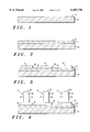
- FIGS. 1-6 are a series of cross-sectional views of an organic electroluminescent device and method of fabrication, in accordance with the present invention.
- FIGS. 1-6 illustrate therein both an organic electroluminescent device and a method for fabricating the same.
- the organic electroluminescent device is fabricated on a substrate 10 having a surface 11 such as that illustrated in FIGS. 1-6.
- the first step in the fabrication process is to provide a substrate upon which the organic electroluminescent device may be fabricated.
- Substrate 10 is preferably transparent, non-electrically conductive, serves as a supportive element and may be fabricated of any of a number of known materials employed in the art.
- the substrate 10 may be fabricated of a glass such as Corning 7059 glass, transparent plastic substrates made of polyolefins, polyethersulfones, polyarylates, and combinations thereof.
- the substrate 10 is fabricated of a glass of quality acceptable for display applications.
- first electrode material 12 which is electrically conductive and optically transparent or at least semi-transparent.
- a first electrode material 12 which is electrically conductive and optically transparent or at least semi-transparent.
- conductive metal oxides such as indium oxide, indium tin oxide (ITO), zinc oxide, zinc tin oxide, conductive transparent polymers such as polyaniline and combinations thereof.
- the electrode 12 may be fabricated of a semi-transparent metal, examples of which include a thin layer (i.e. on the order of less than 500 angstroms) of gold, copper, silver, and combinations thereof.
- the electrode 12 is fabricated of either ITO or zinc oxide. It should be understood that first electrode material 12 is patterned to allow for X-Y addressing of the device as previously described.
- a layer of dielectric material 14 is deposited atop the electrode 12 and the exposed areas (not shown) of the substrate 10.
- the dielectric material may be fabricated or deposited by any of a number of known techniques in the art.
- the layer of material 14 is preferably fabricated of a dielectric media such as photoresists, polyimides, photosensitive polyimides, epoxies, photosensitive epoxies, SiO x , SiN x , SiC x , MgF x , and combinations thereof.
- the layer of dielectric material is fabricated of photosensitive polyimides, deposited to a total thickness of between 5 nm and 200 nm, and preferably between 10 nm and 100 nm.
- dielectric material layer 14 will prevent any electrical shorting between electrically conductive material layer 12 and the upper layer of conductive metal (discussed presently).
- dielectric material layer 14, made of an inorganic dielectric medium, will prevent any contamination from the second dielectric medium (discussed presently), thereby producing a more reliable OED device.
- the layer 14 of dielectric material is patterned into dielectric strips utilizing conventional photolithography or any other well known technique in the art, so as to selectively remove portions of dielectric material 14. This is done so as to form a plurality of exposed areas 15 of electrically conductive material 12, as well as a plurality of dielectric wall structures such as 16 of FIG. 3.
- Each of the wall structures is characterized by a base portion which is adjacent to the layer of electrically conductive material 12, a vertical portion and a top portion which is at the end of the wall structure distanced from the layer 12.
- dielectric material, or strip, 16 in FIG. 3 may also be directly formed by printing methods.
- Shadow mask layer 18 is deposited on the top portion of etched dielectric material 14, exposed areas 15 of electrically conductive material layer 12 and the exposed areas (not shown) of the substrate 10. Shadow mask layer 18 will serve to automatically pattern the second conductive metal layer (discussed previously) positioned thereupon. Shadow mask layer 18 is patterned into dielectric walls by conventional photolithography or any other well known technique in the art. Once shadow mask layer 18 reaches an initial appropriate thickness of approximately 1 to 10 micrometers, photolithography techniques are used to selectively remove portions of shadow mask layer 18 formed on a portion of dielectric material strip 14 and electrically conductive material layer 12.
- Shadow mask layer 18 is preferably fabricated of a dielectric material such as photoresists, polyimides, photosensitive polyimides, epoxies, photosensitive epoxies, SiO x , SiN x , SiC x , MgF x , and combinations thereof.
- shadow mask layer 18, in combination with dielectric material layer 14, will prevent any electrical shorting of the device, more specifically, "cross-talk" between the cathode electrodes and leakage between the anode and the cathode defined by electrically conductive material layer 12 and the second conductive metal layer (discussed shortly).
- the organic layers of an organic electroluminescent device comprises at least one and up to five layers of materials: a hole injecting layer, a hole transport layer, an emissive layer, an electron transport layer, and electron injecting layer.
- the series of layers are illustrated as but one single electroluminescent medium layer 22 deposited on the structure of FIG. 4.
- the organic electroluminescent layers are deposited in the fashion so that they coat both the tops of the wall structures of resist shadow mask layer 18 and dielectric material layer 14, as well as the exposed portions 15 therebetween, specifically, the opening between two adjacent wall structures.
- a layer of organic electroluminescent medium 22 is disposed atop wall structure 16 and 17, on the exposed area of layer 12, between adjacent wall structures.
- the exact organic materials selected for use in the layers of the organic electroluminescent material may be any of those known in the art.
- Organic electroluminescent medium 22 is generally fabricated to a thickness similar to that of dielectric material layer 14, more particularly, organic electroluminescent material layer 22 are generally fabricated between 200-2000 angstroms.
- Layer 22 of organic electroluminescent medium can be deposited by vacuum evaporation.
- Layer 22 of organic electroluminescent medium can also be deposited by other techniques such as injection-fill, spin-coating, roll-coating, dip-coating or doctor-blading from a suitable solution when polymeric materials are used.
- a mixture of the above-mentioned techniques may be needed in cases where a heterostructure array composed of both small organic molecule materials and polymers is to be built.
- the second electrode is typically fabricated of a metal of work function of less than 4 electron volts and at least one other protected metal of higher work function.
- the preferred low work function metal is selected from the group of lithium, magnesium, calcium, strontium, and combinations thereof, while preferred high work function metal is selected from the group of aluminum, indium, copper, gold, silver and combinations thereof.
- second electrode 24 is formed of a alloy of lower work function metal and a high work function metal by co-evaporation.
- the content of the low work function metal and the second electrode can vary from 0.1% to 50% but typically is below about 20%. It should be understood that the layer of metal which defines second electrode 24 is automatically patterned due to the underlying wall structures 16 and 17. Accordingly, no mechanical patterning of second electrode 24 is required during the manufacturing of the OED device of the present invention.
- holes inject from the first electrode (also called the anode) 12 and electrons inject from the second electrode 24 (also known as the cathode), into the organic layers 22 disposed between the electrically conductive electrodes, when an electrical current is applied between the anode and the cathode.
- An electrical current may be applied by connecting the electrodes to electrical current generating means (not shown).
- the electric current generating means attached to both electrode layer 12 and electrodes 24, and will allow holes and electrons to recombine in the organic layer to generate a desired optical characteristic.
- a pixelated organic electroluminescent display device defining a plurality of pixellated picture elements, is provided by means of conventional fabrication processes, without incurring shorting out or cross-talk between the conductive material layers.
- the device of the present invention is amenable to consistent commercial manufacturing line technology, provides for a high throughput or yield, high reliability and low manufacturing costs.
Abstract
Description
Claims (15)
Priority Applications (1)
| Application Number | Priority Date | Filing Date | Title |
|---|---|---|---|
| US08/867,706 US6107736A (en) | 1997-06-02 | 1997-06-02 | Organic electroluminescent display device and method of fabrication |
Applications Claiming Priority (1)
| Application Number | Priority Date | Filing Date | Title |
|---|---|---|---|
| US08/867,706 US6107736A (en) | 1997-06-02 | 1997-06-02 | Organic electroluminescent display device and method of fabrication |
Publications (1)
| Publication Number | Publication Date |
|---|---|
| US6107736A true US6107736A (en) | 2000-08-22 |
Family
ID=25350325
Family Applications (1)
| Application Number | Title | Priority Date | Filing Date |
|---|---|---|---|
| US08/867,706 Expired - Lifetime US6107736A (en) | 1997-06-02 | 1997-06-02 | Organic electroluminescent display device and method of fabrication |
Country Status (1)
| Country | Link |
|---|---|
| US (1) | US6107736A (en) |
Cited By (9)
| Publication number | Priority date | Publication date | Assignee | Title |
|---|---|---|---|---|
| US6249084B1 (en) * | 1998-01-14 | 2001-06-19 | Sharp Kabushiki Kaisha | Electroluminescence display panel and production method of the same |
| US6414432B1 (en) * | 1999-02-15 | 2002-07-02 | Futaba Corporation | Organic EL device and method for manufacturing same |
| US6657380B2 (en) * | 2000-05-03 | 2003-12-02 | Ritek Corporation | Organic electroluminescent display panel having a polyimide-isolating wall of reverse-trapezoid cross-section with electric, thermal and mechanical stability |
| US20030227255A1 (en) * | 2002-06-10 | 2003-12-11 | Institute Of Materials Research And Engineering | Patterning of electrodes in oled devices |
| US6686693B1 (en) * | 1999-09-06 | 2004-02-03 | Futaba Denshi Kogyo Kabushiki Kaisha | Organic electroluminescent device with disjointed electrodes arranged in groups |
| US20040101988A1 (en) * | 2000-06-06 | 2004-05-27 | Roman Paul J. | Deposition of permanent polymer structures for OLED fabrication |
| US20040113545A1 (en) * | 2002-09-19 | 2004-06-17 | Lg.Philips Lcd Co., Ltd. | Transmissive-type organic electroluminescent display device and fabricating method of the same |
| US7205964B1 (en) * | 1998-09-02 | 2007-04-17 | Seiko Epson Corporation | Light source and display device |
| US20140110023A1 (en) * | 2010-04-07 | 2014-04-24 | Samsung Electro-Mechanics Co., Ltd. | Printed circuit board and method of manufacturing the same |
Citations (7)
| Publication number | Priority date | Publication date | Assignee | Title |
|---|---|---|---|---|
| US4797890A (en) * | 1985-12-24 | 1989-01-10 | Mitsubishi Cable Industries, Ltd. | Semiconductor light emitting device with vertical light emission |
| US5188901A (en) * | 1987-03-31 | 1993-02-23 | Hoya Corporation | Electroluminescent panel having a fluoroesin layer |
| US5276380A (en) * | 1991-12-30 | 1994-01-04 | Eastman Kodak Company | Organic electroluminescent image display device |
| US5346776A (en) * | 1988-12-29 | 1994-09-13 | Sharp Kabushiki Kaisha | Electroluminescent panel |
| US5445899A (en) * | 1992-12-16 | 1995-08-29 | Westinghouse Norden Systems Corp. | Color thin film electroluminescent display |
| US5479070A (en) * | 1990-05-18 | 1995-12-26 | Fuji Xerox Co., Ltd. | Light-emitting element device |
| US5773931A (en) * | 1996-09-06 | 1998-06-30 | Motorola, Inc. | Organic electroluminescent device and method of making same |
-
1997
- 1997-06-02 US US08/867,706 patent/US6107736A/en not_active Expired - Lifetime
Patent Citations (7)
| Publication number | Priority date | Publication date | Assignee | Title |
|---|---|---|---|---|
| US4797890A (en) * | 1985-12-24 | 1989-01-10 | Mitsubishi Cable Industries, Ltd. | Semiconductor light emitting device with vertical light emission |
| US5188901A (en) * | 1987-03-31 | 1993-02-23 | Hoya Corporation | Electroluminescent panel having a fluoroesin layer |
| US5346776A (en) * | 1988-12-29 | 1994-09-13 | Sharp Kabushiki Kaisha | Electroluminescent panel |
| US5479070A (en) * | 1990-05-18 | 1995-12-26 | Fuji Xerox Co., Ltd. | Light-emitting element device |
| US5276380A (en) * | 1991-12-30 | 1994-01-04 | Eastman Kodak Company | Organic electroluminescent image display device |
| US5445899A (en) * | 1992-12-16 | 1995-08-29 | Westinghouse Norden Systems Corp. | Color thin film electroluminescent display |
| US5773931A (en) * | 1996-09-06 | 1998-06-30 | Motorola, Inc. | Organic electroluminescent device and method of making same |
Cited By (12)
| Publication number | Priority date | Publication date | Assignee | Title |
|---|---|---|---|---|
| US6249084B1 (en) * | 1998-01-14 | 2001-06-19 | Sharp Kabushiki Kaisha | Electroluminescence display panel and production method of the same |
| US7205964B1 (en) * | 1998-09-02 | 2007-04-17 | Seiko Epson Corporation | Light source and display device |
| US6414432B1 (en) * | 1999-02-15 | 2002-07-02 | Futaba Corporation | Organic EL device and method for manufacturing same |
| US6686693B1 (en) * | 1999-09-06 | 2004-02-03 | Futaba Denshi Kogyo Kabushiki Kaisha | Organic electroluminescent device with disjointed electrodes arranged in groups |
| US6657380B2 (en) * | 2000-05-03 | 2003-12-02 | Ritek Corporation | Organic electroluminescent display panel having a polyimide-isolating wall of reverse-trapezoid cross-section with electric, thermal and mechanical stability |
| US20040101988A1 (en) * | 2000-06-06 | 2004-05-27 | Roman Paul J. | Deposition of permanent polymer structures for OLED fabrication |
| US7427529B2 (en) | 2000-06-06 | 2008-09-23 | Simon Fraser University | Deposition of permanent polymer structures for OLED fabrication |
| US20030227255A1 (en) * | 2002-06-10 | 2003-12-11 | Institute Of Materials Research And Engineering | Patterning of electrodes in oled devices |
| US7221093B2 (en) * | 2002-06-10 | 2007-05-22 | Institute Of Materials Research And Engineering | Patterning of electrodes in OLED devices |
| US20040113545A1 (en) * | 2002-09-19 | 2004-06-17 | Lg.Philips Lcd Co., Ltd. | Transmissive-type organic electroluminescent display device and fabricating method of the same |
| US7173371B2 (en) * | 2002-09-19 | 2007-02-06 | Lg.Philips Lcd Co., Ltd. | Transmissive-type organic electroluminescent display device and fabricating method of the same |
| US20140110023A1 (en) * | 2010-04-07 | 2014-04-24 | Samsung Electro-Mechanics Co., Ltd. | Printed circuit board and method of manufacturing the same |
Similar Documents
| Publication | Publication Date | Title |
|---|---|---|
| US5804917A (en) | Organic electroluminescent display device and method for manufacturing same | |
| US6140765A (en) | Organic electroluminescent display panel having a plurality of ramparts formed on the first and second bus electrodes | |
| US5773931A (en) | Organic electroluminescent device and method of making same | |
| US5953587A (en) | Method for deposition and patterning of organic thin film | |
| US6794676B2 (en) | Fabrication of organic light emitting diode using selective printing of conducting polymer layers | |
| US6214631B1 (en) | Method for patterning light emitting devices incorporating a movable mask | |
| US7642109B2 (en) | Electrical connection in OLED devices | |
| KR19990072868A (en) | Display devices | |
| US7122956B2 (en) | OLED display and method of manufacturing such display | |
| JP2005327674A (en) | Organic electroluminescent display element, display device having the same, and manufacturing method thereof | |
| US7091666B2 (en) | Organic electroluminescent device | |
| US7221094B2 (en) | Electroluminescent device and method of manufacturing the same | |
| US6107736A (en) | Organic electroluminescent display device and method of fabrication | |
| JP3736179B2 (en) | Organic thin film light emitting device | |
| KR100294669B1 (en) | organic EL display panel and method for fabricating the same | |
| JP3517099B2 (en) | Method for manufacturing organic electroluminescence device | |
| KR100975295B1 (en) | Electrical device and method for manufacturing an electrical device | |
| JP2009181766A (en) | Organic el display, and method of manufacturing organic el display | |
| US7473924B2 (en) | Electroluminescent device with a blocking layer and a dummy electrode region | |
| US7498737B2 (en) | Method of manufacturing an organic electronic device and organic electronic device | |
| US7375461B2 (en) | Organic, electroluminescent display and method for producing the same | |
| EP2234162B1 (en) | Organic electroluminescent display panel and method for fabricating the same | |
| JP3755727B2 (en) | Organic thin film light emitting display panel and method for manufacturing the same | |
| WO1999026730A1 (en) | Method of fabricating and patterning oleds | |
| JP3653942B2 (en) | Organic light emitting device and method for manufacturing the same |
Legal Events
| Date | Code | Title | Description |
|---|---|---|---|
| AS | Assignment |
Owner name: MOTOROLA, INC., ILLINOIS Free format text: ASSIGNMENT OF ASSIGNORS INTEREST;ASSIGNORS:SHI, SONG Q.;SO, FRANKY;LEE, HSING-CHUNG;REEL/FRAME:008581/0181 Effective date: 19970529 |
|
| STCF | Information on status: patent grant |
Free format text: PATENTED CASE |
|
| FPAY | Fee payment |
Year of fee payment: 4 |
|
| FPAY | Fee payment |
Year of fee payment: 8 |
|
| AS | Assignment |
Owner name: MOTOROLA SOLUTIONS, INC., ILLINOIS Free format text: CHANGE OF NAME;ASSIGNOR:MOTOROLA, INC;REEL/FRAME:025909/0661 Effective date: 20110104 |
|
| AS | Assignment |
Owner name: MOTOROLA SOLUTIONS, INC., ILLINOIS Free format text: CHANGE OF NAME;ASSIGNOR:MOTOROLA, INC;REEL/FRAME:026081/0001 Effective date: 20110104 |
|
| AS | Assignment |
Owner name: UNIVERSAL DISPLAY CORPORATION, NEW JERSEY Free format text: ASSIGNMENT OF ASSIGNORS INTEREST;ASSIGNOR:MOTOROLA SOLUTIONS, INC.;REEL/FRAME:026620/0812 Effective date: 20110316 |
|
| FPAY | Fee payment |
Year of fee payment: 12 |