US6118676A - Dynamic voltage sag correction - Google Patents
Dynamic voltage sag correction Download PDFInfo
- Publication number
- US6118676A US6118676A US09/433,993 US43399399A US6118676A US 6118676 A US6118676 A US 6118676A US 43399399 A US43399399 A US 43399399A US 6118676 A US6118676 A US 6118676A
- Authority
- US
- United States
- Prior art keywords
- voltage
- inverter
- line voltage
- voltage sag
- output
- Prior art date
- Legal status (The legal status is an assumption and is not a legal conclusion. Google has not performed a legal analysis and makes no representation as to the accuracy of the status listed.)
- Expired - Lifetime
Links
Images


Classifications
-
- H—ELECTRICITY
- H02—GENERATION; CONVERSION OR DISTRIBUTION OF ELECTRIC POWER
- H02J—CIRCUIT ARRANGEMENTS OR SYSTEMS FOR SUPPLYING OR DISTRIBUTING ELECTRIC POWER; SYSTEMS FOR STORING ELECTRIC ENERGY
- H02J3/00—Circuit arrangements for ac mains or ac distribution networks
- H02J3/28—Arrangements for balancing of the load in a network by storage of energy
-
- H—ELECTRICITY
- H02—GENERATION; CONVERSION OR DISTRIBUTION OF ELECTRIC POWER
- H02J—CIRCUIT ARRANGEMENTS OR SYSTEMS FOR SUPPLYING OR DISTRIBUTING ELECTRIC POWER; SYSTEMS FOR STORING ELECTRIC ENERGY
- H02J3/00—Circuit arrangements for ac mains or ac distribution networks
- H02J3/18—Arrangements for adjusting, eliminating or compensating reactive power in networks
- H02J3/1807—Arrangements for adjusting, eliminating or compensating reactive power in networks using series compensators
- H02J3/1814—Arrangements for adjusting, eliminating or compensating reactive power in networks using series compensators wherein al least one reactive element is actively controlled by a bridge converter, e.g. unified power flow controllers [UPFC]
-
- H—ELECTRICITY
- H02—GENERATION; CONVERSION OR DISTRIBUTION OF ELECTRIC POWER
- H02M—APPARATUS FOR CONVERSION BETWEEN AC AND AC, BETWEEN AC AND DC, OR BETWEEN DC AND DC, AND FOR USE WITH MAINS OR SIMILAR POWER SUPPLY SYSTEMS; CONVERSION OF DC OR AC INPUT POWER INTO SURGE OUTPUT POWER; CONTROL OR REGULATION THEREOF
- H02M5/00—Conversion of ac power input into ac power output, e.g. for change of voltage, for change of frequency, for change of number of phases
- H02M5/40—Conversion of ac power input into ac power output, e.g. for change of voltage, for change of frequency, for change of number of phases with intermediate conversion into dc
- H02M5/42—Conversion of ac power input into ac power output, e.g. for change of voltage, for change of frequency, for change of number of phases with intermediate conversion into dc by static converters
- H02M5/44—Conversion of ac power input into ac power output, e.g. for change of voltage, for change of frequency, for change of number of phases with intermediate conversion into dc by static converters using discharge tubes or semiconductor devices to convert the intermediate dc into ac
- H02M5/453—Conversion of ac power input into ac power output, e.g. for change of voltage, for change of frequency, for change of number of phases with intermediate conversion into dc by static converters using discharge tubes or semiconductor devices to convert the intermediate dc into ac using devices of a triode or transistor type requiring continuous application of a control signal
- H02M5/458—Conversion of ac power input into ac power output, e.g. for change of voltage, for change of frequency, for change of number of phases with intermediate conversion into dc by static converters using discharge tubes or semiconductor devices to convert the intermediate dc into ac using devices of a triode or transistor type requiring continuous application of a control signal using semiconductor devices only
-
- Y—GENERAL TAGGING OF NEW TECHNOLOGICAL DEVELOPMENTS; GENERAL TAGGING OF CROSS-SECTIONAL TECHNOLOGIES SPANNING OVER SEVERAL SECTIONS OF THE IPC; TECHNICAL SUBJECTS COVERED BY FORMER USPC CROSS-REFERENCE ART COLLECTIONS [XRACs] AND DIGESTS
- Y02—TECHNOLOGIES OR APPLICATIONS FOR MITIGATION OR ADAPTATION AGAINST CLIMATE CHANGE
- Y02E—REDUCTION OF GREENHOUSE GAS [GHG] EMISSIONS, RELATED TO ENERGY GENERATION, TRANSMISSION OR DISTRIBUTION
- Y02E40/00—Technologies for an efficient electrical power generation, transmission or distribution
- Y02E40/10—Flexible AC transmission systems [FACTS]
Definitions
- This invention pertains generally to the field of electric power supplies and electric power conversion systems, and more particularly to systems for providing power line conditioning and for correcting voltage sag and drop conditions in a power line providing electric power to a load.
- a variety of power conversion circuits have been developed for converting electric power at one voltage level or frequency to another voltage level or frequency.
- a commonly used device for providing an output voltage signal to a load at a different level than that of the available input voltage signal is a step-up or a step-down transformer, which may be provided either on the input or output side of a power conversion circuit.
- Such transformers are relatively large, heavy, and expensive. If a power conversion circuit is intended to maintain an output voltage at a desired level despite variations in the input voltage level (or to allow the output voltage to be adjusted to a desired level at a constant input voltage level) more complex transformer structures may be required.
- some power conditioning circuits utilize tap-changing transformers, in which the primary transformer winding includes a number of separate taps which are connected to the power conditioning circuit input terminals by static switches.
- a controller circuit monitors the power conditioning circuit output voltage and switches the proper static switches on the input side to maintain approximately the desired voltage level on the output side.
- Tap changing transformers require many switching devices, such as thyristors, and only permit coarse control of the output voltage. Furthermore, distortion of the voltage on a load cannot be well controlled using such a transformer.
- ferroresonant transformer is connected in a circuit which provides passive compensation for short term changes in an input voltage level.
- Ferroresonant transformers are widely used, and provide reasonable voltage regulation, typically plus or minus 4% at the transformer output for a minus 20% to plus 10% change in the transformer input voltage.
- output distortion can be sensitive to load input harmonics, and the input currents drawn may have undesirable power factors and distortion levels when ferroresonant transformers are employed for voltage regulation.
- Power conditioning circuits employing tap changing or ferroresonant transformers are limited in application by the presence of the low frequency transformer, which must be able to handle full rated power.
- the transformer for a one kilovolt ampere (KVA) line conditioner employing such a transformer, the transformer by itself can weigh over 30 to 40 pounds, and is the major component determining the size of the cabinet containing the power conditioning apparatus.
- KVA one kilovolt ampere
- Voltage boosting circuits for increasing an available AC input voltage level to a desired AC output voltage level without employing a tap changing or ferroresonant transformer have been developed. Such circuits typically require that the input AC voltage signal be fully converted to a DC voltage level on a DC bus. The DC voltage is then inverted to AC power utilizing a full bridge inverter circuit. Such systems typically require an inverter employing four switching devices to provide a single phase AC output voltage signal and an inverter employing six switching devices to provide a three phase AC output voltage signal.
- U.S. Pat. No. 5,099,410 to Deepakraj M. Divan, describes a power conversion circuit which converts an AC source voltage at one voltage level to an AC output voltage at a different voltage level without using a transformer and with a minimum number of solid state switching devices employed.
- the basic power conversion circuit described in this patent includes a pair of rectifying devices connected together at a first node, a pair of capacitors connected together at a second node, and a pair of controllable switching devices connected together at a third node, with the pairs of rectifying devices, capacitors, and switching devices connected in parallel by DC bus lines.
- the three nodes serve as three terminals of the power conversion circuit.
- the first terminal or node is common to both the input power source and the load, the second node or terminal is connected to the source, and the third node or terminal is connected to the load.
- the power conversion circuit can be controlled by a system controller to provide a peak-to-peak output voltage to the load which is substantially double the peak-to-peak input voltage.
- the rectifying devices charge the capacitors to the peak of the input voltage.
- the system controller provides turn-on and turn-off signals to the controllable switching devices alternately and in phase with the input voltage so that the voltage across one of the charged capacitors plus the input voltage is applied to the load during one half cycle of the input voltage waveform and the voltage across the other charged capacitor and the input voltage of the opposite polarity is applied to the load during the other half of the input voltage waveform.
- the circuit can be controlled to provide an output voltage signal across the load that can be varied from substantially zero to substantially twice the peak-to-peak input voltage.
- the switching devices are switched on for a duty cycle which is less than a full half cycle of the input voltage waveform.
- pulse width modulation may be utilized in controlling the switching devices so that a desired effective AC voltage level is provided across the load. Only two switching devices are required to obtain such operation.
- Power line conditioning systems are used to provide compensation for and correction of voltage sags and drops in the signal provided on power lines to a load.
- Industrial process disruptions due to poor electrical power quality cause billions of dollars per year in lost productivity in the United States alone.
- Deep voltage sags and momentary voltage interruptions have been called the most important power quality concerns affecting most industrial and commercial electrical power customers.
- Productivity losses can occur, for example, when momentary electrical power interruptions cause factory robots to "lockup", resulting in entire production lines stopping and a significant amount of scrapped product.
- a momentary interruption of electrical power for as little as one cycle can cause high intensity discharge (HID) lighting to restart, resulting in a delay of as much as 20 minutes before factory lighting can be restored.
- CBEMA Computer Business Equipment Manufacturers Association
- surge suppressors are employed to provide load voltage protection for very short duration voltage transients caused, e.g., by lighting strikes.
- Surge suppressors are very inexpensive, but provide no compensation for voltage sags or extended power outages.
- Relatively low cost voltage regulators typically employing tap changing transformers, have been used to provide voltage sag compensation.
- Such voltage regulators are much more expensive than surge suppressors, and are only of limited effectiveness in responding to voltage transients, due to the slow response of such systems.
- the slow response of tap changing systems also limits their ability to provide correction of voltage sags.
- a voltage sag lasting less than one cycle may cause an industrial system disruption.
- low cost voltage regulators employing tap changing transformers are typically only available for the correction of voltage sags to no lower than 80% of nominal voltage levels. Such systems provide no protection for larger voltage sags or complete power outages.
- Higher cost voltage regulators, employing constant voltage ferroresonant transformers have faster response times, and thus should be capable of providing correction for transient events.
- systems employing such constant voltage transformers typically only provide effective power line conditioning for voltage sags to no less than 70% of nominal voltage levels. Such systems do not provide any power correction for larger voltage sags or extended power outages.
- power conditioning systems employing constant voltage transformers are much more expensive than systems employing tap changing transformers, and are also much more heavy and bulky.
- UPS Uninterruptible power supplies
- the typical UPS includes at least a battery and an inverter. When a power line voltage drop is detected, the power line is disconnected from the load, and the UPS inverter is turned on to provide AC power to the load from the battery until a normal voltage level is restored on the power line.
- the system battery is recharged by a rectifier, or by controlling the inverter to operate as a rectifier, with power from the power line when normal power line voltage is restored.
- UPS can typically respond quickly to power line transients, voltage sags, and voltage drops, and can provide power to a load from the battery for several minutes, if necessary, in response to an extended power line outage.
- UPS systems are, however, relatively very expensive. Such systems typically employ many expensive power switching devices which are rated to operate to provide power to a load for an extended duration without interruption.
- the UPS battery is also typically very expensive, heavy, and bulky, and must be replaced periodically.
- the prior art thus fails to provide a lightweight compact inexpensive power conditioning system with a rapid response time for providing correction of the vast majority of power line conditions which can cause productivity losses.
- the present invention provides a low cost, small size, lightweight, and highly effective system and method for providing dynamic power line voltage sag correction.
- a dynamic voltage sag corrector in accordance with the present invention provides correction of the most common power quality related events which may affect the operation of a load provided with electrical power on power lines from a utility power source.
- a dynamic voltage sag corrector in accordance with the present invention is connected to power lines between an unprotected utility power source and a load to provide a protected voltage output to the load.
- the dynamic voltage sag corrector includes a static bypass switch and a regulator/storage module connected together in parallel. Under normal power line conditions, the static bypass switch is closed, and a normal input line voltage signal is provided directly to the load.
- the regulator/storage module provides power to the load from both the available input line voltage and the storage capacitors, to provide an output voltage signal to the load at a pre-voltage sag voltage level until the input voltage level is restored to the pre-fault level.
- the circuit components used in the regulator/storage module are selected such that the dynamic voltage sag corrector is capable of providing compensation for input voltage transients, sags, and drops for a duration of several seconds.
- a dynamic voltage sag corrector in accordance with the present invention provides correction for the vast majority of utility power quality related events encountered, with reduced component size, weight, and cost.
- a dynamic voltage sag corrector in accordance with the present invention includes a static bypass switch, which may be implemented using conventional power switching devices, such as thyristors connected in anti-parallel, to conduct in opposite directions.
- the regulator/storage module is connected in parallel with the static bypass switch.
- the regulator/storage module includes a pair of rectifying devices, e.g., diodes, connected together at a first node, a pair of storage capacitors connected together at second node, and a pair of controllable inverter switching devices, e.g., transistors, connected together at a third node, with the pairs of rectifying devices, storage capacitors, and inverter switching devices connected in parallel by DC bus lines.
- the three nodes serve as three terminals of the regulator/storage module.
- the first terminal or node is common to both the input power source and the load, the second node or terminal is connected to the input power source, and the third node or terminal is connected to the load.
- a low-pass filter is preferably connected between the third node or terminal and the load.
- the dynamic voltage sag corrector operates in the bypass mode. As long as the input line voltage remains at more than a selected percentage of the nominal input voltage level, the static bypass switch remains closed, and power is provided directly from the input line to the load via the static bypass switch, bypassing the regulator/storage module. During such normal operation, the storage capacitors in the regulator/storage module are each charged to near the peak voltage of the normal input voltage signal.
- the dynamic voltage sag corrector is controlled by a system controller, which may be implemented using a microprocessor, discrete components, or a combination thereof.
- the input voltage and/or the output voltage provided to the load is monitored by the system controller. If a sag in the voltage provided to the load below a selected percentage of the nominal output voltage level is detected, the system controller opens the static bypass switch to interrupt the direct path from the input line to the load.
- the inverter switching devices in the regulator/storage module are then controlled by the system controller to boost the available incoming line voltage to a boosted output voltage level which is provided to the load.
- the system controller provides turn-on and turn-off signals to the controllable inverter switching devices alternately such that the voltage across one of the charged storage capacitors plus the available input voltage is provided to the load during one portion of the input voltage waveform and such that the voltage across the other charged storage capacitor and the available input voltage of the opposite polarity is applied to the load during other portions of the input voltage waveform.
- the inverter switching devices are typically switched on for a duty cycle which is less than a full half cycle of the input voltage waveform.
- pulse width modulation may be utilized in controlling the inverter switching devices to provide the desired AC voltage signal to the load.
- a low-pass filter removes high frequency switching components from the inverter output signal, to provide a nearly sinusoidal signal to the load.
- a dynamic voltage sag corrector in accordance with the present invention preferably includes several safety features to protect the circuit from damage due to extreme operating conditions.
- the current through the inverter switching devices in the regulator/storage module is preferably monitored by the system controller. If the inverter switching device current exceeds a safe operating value for the switching devices, the system controller turns the inverter switching devices off, and closes the static bypass switch to reconnect the load directly to the unprotected input voltage signal.
- the load current is preferably also monitored by the system controller during normal power line operation, when the load is being provided power directly from the input line via the static bypass switch.
- the preferred regulator/storage module circuit topology employed in a dynamic voltage sag corrector in accordance with the present invention may be operated as a voltage doubler for an indefinite period of time.
- a dynamic voltage sag corrector in accordance with the present invention is capable of restoring an input voltage sag to 45% of the nominal input voltage level to an output voltage level of 90% of the nominal input voltage level for an indefinite period.
- the duration for which the regulator/storage module can restore the output voltage to a near normal level is limited by the energy stored in the storage capacitors in the regulator/storage module.
- the ability of the system to provide dynamic voltage sag correction for extreme voltage sags and complete voltage drops can be enhanced by increasing the size of the storage capacitors in the regulator/storage module. This, however, will increase the cost, size, and weight of the system.
- An alternative approach is to control the regulator/storage module to provide power only to a priority load portion of an entire load under such extreme voltage sag/voltage drop conditions.
- the priority load may represent a critical subset of the entire load supplied through the dynamic voltage sag corrector. During normal power line operation, the entire load is provided power from an input line through the static bypass switch.
- the entire load is provided with power via the regulator/storage module, which is capable of compensating for such voltage sags indefinitely.
- the regulator/storage module is connected only to provide power to the priority portion of the load, the balance of the load is disconnected from the regulator/storage module. In this manner, the regulator/storage module is able to support the priority load from the energy stored in the storage capacitors for a longer duration than the regulator/storage module could support the entire load.
- the priority load may thus be provided with power for a sufficient duration to effect an orderly shutdown.
- a dynamic voltage sag corrector in accordance with the present invention may be configured to compensate for voltage surges as well as voltage sags. Voltage surges are relatively rare short-lived occurrences which can, nevertheless, interrupt the operation of or damage a load.
- the system controller of the dynamic voltage sag corrector may monitor the input line voltage level and/or the voltage level provided to a load for a voltage surge condition, e.g., a condition where the input line voltage exceeds a certain percentage greater than 100% of the nominal input voltage level. If a voltage surge is detected, the system controller opens the static bypass switch, and the load is provided with power at the nominal voltage level by operation of the regulator/storage module until the nominal input line voltage level is restored.
- An energy dissipation circuit which may be implemented as a dissipation resistor connected in series with a dissipation switching device across the DC bus lines of the regulator/storage module, may be provided in the regulator/storage module and controlled by the system controller to dissipate the excess energy stored in the storage capacitors as a result of the voltage surge condition.
- a dynamic voltage sag corrector in accordance with the present invention may be implemented for single phase or multiphase applications.
- a three phase dynamic voltage sag corrector in accordance with the present invention may be implemented using three single phase sag correctors, one such single phase corrector provided for each phase. Cross-coupling between the three singlephase sag correctors may be provided to handle deeper single-line faults.
- a three phase dynamic voltage sag corrector in accordance with the present invention may be implemented using a regulator/storage module which is implemented using a single three-phase four leg inverter having a single pair of storage capacitors connected across DC bus lines thereof, or three single-phase full bridge inverters connected in parallel with a storage capacitor across DC bus lines.
- the storage capacitor(s) may be charged via a multiphase rectifier connected across the three phase input lines between the three phase input lines and the DC bus lines of the regulator/storage module.
- the three-phase outputs of the three phase inverter are coupled to the three-phase power lines via a transformer to inject a voltage boosting signal in series with the available three-phase input power to restore the voltage level provided to the load under voltage sag conditions to at or near the normal level.
- a switching device may preferably be connected across the DC bus lines between the rectifier and the storage capacitor(s), with a diode connected in series with the DC bus line between the switch and the storage capacitor. If a fault or open circuit breaker causes a complete interruption in the current provided to the load on the three-phase input power lines, the switch connected in parallel with the multiphase rectifier may be closed, thereby providing an effective short circuit on the input line side of the transformer, allowing current flow through the transformer so that power can be delivered from the inverter through the transformer to the three-phase power lines and, therefore, to a load.
- This switch may also be controlled to operate as a boost converter, to charge the storage capacitor(s) to a level higher than the available input line-to-line voltage level, or to interface a high capacity energy storage device, such as an ultra capacitor, to the inverter.
- a dynamic voltage sag corrector in accordance with the present invention provides a very low cost solution to the vast majority of power quality problems encountered by industrial, commercial, and residential power users.
- a dynamic voltage sag corrector provides surge suppression, protects against voltage sags, and provides ride through for short power outages.
- a dynamic voltage sag corrector corrects for all power quality problems except for extended power outages, which occur very rarely in the United States and other industrialized nations. All of these features are achieved, in accordance with the present invention, by a dynamic voltage sag corrector which may be made for a fraction of the cost, and which is a fraction of the size and weight, of competitive solutions.
- the cost, size, and weight advantages of a dynamic voltage sag corrector in accordance with the present invention are achieved by selecting the operating characteristics of the sag corrector to maximize the ability of the corrector to protect a load from the vast majority of voltage surge, sag, and drop conditions which are likely to be encountered, while minimizing the rating of the circuit components which are required to provide such operating characteristics.
- the circuit components required to provide desired dynamic voltage sag correction operating characteristics are selected based on the thermal rating characteristics of the components.
- the inverter switching devices employed in the regulator/storage module of a dynamic voltage sag corrector in accordance with the present invention are not in operation most of the time, when normal input power is provided directly to a load via the static bypass switch.
- the inverter switching devices are activated from a cold state. Inverter switching devices having a smaller power rating can thus be selected, since switching devices of a given rating can be operated from a cold state for a longer duration then from a warm state.
- a dynamic voltage sag corrector in accordance with the present invention may provide compensation for a voltage sag to approximately 50% of the nominal input voltage level continuously, most voltage sags only last for a limited period of time, e.g., 1-2 seconds.
- the voltage rating of the inverter switching devices employed in the dynamic voltage sag corrector can be reduced further, by limiting the operating time of the inverter to the duration of 90-95% of all voltage sag conditions which will be encountered.
- Designing the dynamic voltage sag corrector circuit for short term voltage sags and outages (1-2 seconds) significantly reduces the cost and size of the circuit components which must be employed. Longer term voltage sag and drop events are rare, and typically do not occur continuously.
- the operating duration for which a dynamic voltage sag corrector of a given rating can provide correction for a voltage sag or drop condition may be extended when the circuit component temperatures are lower.
- the temperatures or operating time of selected components in the dynamic voltage sag corrector may be monitored by the system controller.
- Such monitored components may typically include, for example, the inverter switching devices in the regulator/storage module. If the monitored component temperatures are greater than a selected temperature level, or have just been operated, operation of the inverter may be limited to a short duration. Longer operation of the inverter may be allowed if the component temperatures are less than the selected temperature level or if the components have not been operated recently.
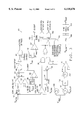
- FIG. 1 is a schematic block diagram of a dynamic voltage sag corrector in accordance with the present invention.
- FIG. 2 is a schematic circuit diagram of a dynamic voltage sag corrector in accordance with the present invention.
- FIG. 3 is a schematic block diagram of a system controller for a dynamic voltage sag corrector in accordance with the present invention.
- FIG. 4 is a schematic circuit diagram of an alternative embodiment of a dynamic voltage sag corrector in accordance with the present invention wherein the dynamic voltage sag corrector is configured to provide voltage sag correction to a priority portion of a load in response to extreme voltage sag/drop conditions.
- FIG. 5 is a schematic circuit diagram of another alternative embodiment of a dynamic voltage sag corrector in accordance with the present invention wherein the dynamic voltage sag corrector includes a dissipation circuit for dissipating excess energy stored in the circuit as a result of a voltage surge condition for which correction is provided by the dynamic voltage sag corrector.
- FIG. 6 is a schematic circuit diagram of an exemplary three phase embodiment of a dynamic voltage sag corrector in accordance with the present invention.
- FIG. 7 is a schematic circuit diagram of another exemplary three phase embodiment of a dynamic voltage sag corrector in accordance with the present invention.
- FIG. 8 is a schematic circuit diagram of yet another exemplary three-phase embodiment of a dynamic voltage sag corrector in accordance with the present invention.
- FIG. 9 is a schematic circuit diagram of a generic three-phase embodiment of a dynamic voltage sag corrector in accordance with the present invention for injecting a three-phase power signal in series with three-phase power lines and including an additional switching device and diode for assuring operation during a complete break on the three-phase power lines.
- FIG. 10 is a waveform diagram illustrating input and output voltages of a dynamic voltage sag corrector in accordance with the present invention during an input voltage sag condition.
- FIGS. 11 and 12 illustrate trip voltage regions for a high intensity discharge light as unprotected by a dynamic voltage sag corrector in accordance with the present invention and as protected by a dynamic voltage sag corrector in accordance with the present invention, respectively.
- a dynamic voltage sag corrector 20 in accordance with the present invention is illustrated in schematic block diagram form in, and will be described with reference to, FIG. 1.
- a dynamic voltage sag corrector 20 in accordance with the present invention is adapted to be connected between an AC power source 22 and an AC load 24.
- a dynamic voltage sag corrector 20 in accordance with the present invention may be employed to provide voltage sag correction for single or multiple phase voltage sources 22 and loads 24, and can be configured to provide protected power to a load 24 from an unprotected voltage source 22 at any voltage or power level.
- the two main components of a dynamic voltage sag corrector 20 in accordance with the present invention are a static bypass switch 26 and a regulator/storage module 28.
- the regulator/storage module 28 includes a system controller (not shown in FIG. 1) for monitoring the voltage level provided by the voltage source 22 to the load 24 and for controlling the static bypass switch 26 and the regulator/storage module 28.
- a system controller for monitoring the voltage level provided by the voltage source 22 to the load 24 and for controlling the static bypass switch 26 and the regulator/storage module 28.
- the static bypass switch 26 is closed, and power is provided directly from the source 22 to the load 24 via the static bypass switch 26.
- the system controller in the regulator/storage module 28 detects a drop of the input voltage level provided by the source 22 by more than an acceptable amount, the system controller closes the static bypass switch 26 and controls the regulator/storage module 28 to provide AC power at or near the nominal voltage level to the load from the regulator/storage module 28.
- a dynamic voltage sag corrector 20 in accordance with the present invention is capable of providing voltage sag compensation for a duration sufficient to provide correction of the vast majority of voltage sag conditions likely to occur, without requiring the use of large energy storage devices.
- the circuit components in the regulator/storage module are selected such that the regulator/storage module 28 is capable of providing a protected output voltage signal to the load 24 for the vast majority of source voltage sags and drops which will be encountered, but not for rarely occurring extended power outages, to thereby provide a dynamic voltage sag corrector of significantly reduced size, weight, and cost
- FIG. 2 A more detailed schematic circuit diagram of an exemplary dynamic voltage sag corrector 20 in accordance with the present invention is presented in, and will be described with reference to, FIG. 2.
- the exemplary dynamic voltage sag corrector 20 is adapted to be connected at input terminals 30 and 31 to a source of AC input voltage V ACIN and at output terminals 32 and 33 to a load which is provided with AC output voltage V ACOUT .
- AC bus lines 34 and 35 connect input terminal 30 to output terminal 32 and input terminal 31 to output terminal 33, respectively.
- Circuit breakers 36 connected in series with one or both of the AC bus lines 34 and 35, are preferably provided to automatically disconnect the dynamic voltage sag corrector 20 (and a load connected thereto) from the input voltage source if the current through the dynamic voltage sag corrector 20 from the source to the load becomes excessive due to a fault condition, such as a short circuit in the load.
- the circuit breaker 36 may be implemented in a conventional manner. As long as the circuit breakers 36 are closed, the dynamic voltage sag corrector 20 is powered up and in operation to provide a protected output voltage signal at output terminals 32 and 33 to a load.
- a dynamic voltage sag corrector 20 in accordance with the present invention includes a static bypass switch 26 and a regulator/storage module 28.
- the static bypass switch 26 is connected in series with one of the AC bus lines 34 between input terminal 30 and output terminal 32 of the dynamic voltage sag corrector 20. (The static bypass switch 26 may be connected in series with either of the AC bus lines 34 or 35.)
- the static bypass switch 26 may be implemented in a conventional manner to carry an AC voltage signal on the AC bus line 34 between the input 30 and output 32 terminals when the switch 26 is closed. Conventional solid state switching devices may be used to implement the static bypass switch 26.
- anti-parallel connected thyristors may preferably be used to implement the static bypass switch 26.
- power transistor switching devices similarly connected, may be used to implement the static bypass switch 26.
- the type of power switching devices employed in the static bypass switch 26, and the rating of such devices, will depend upon the voltage level which is to be normally conducted through and blocked by the static bypass switch 26 from the input terminals 30 and 31 to a load connected to the output terminals 32 and 33 of the dynamic voltage sag corrector 20.
- the regulator/storage module 28 is preferably implemented as an AC power conversion circuit which employs a minimum number of switching devices to provide a corrected output voltage signal to a load connected to the output terminals 32 and 33 when there is a sag or drop in the source voltage signal V ACIN provided on the input terminals 30 and 31 of the voltage sag corrector 20.
- a variation of the AC power conversion circuit illustrated and described in U.S. Pat. No. 5,099,410 is preferably employed for this purpose.
- the specification of U.S. Pat. No. 5,099,410 is hereby incorporated herein by reference.
- the preferred regulator/storage module circuit 28 has three terminals or nodes, marked I, II, and III in FIGS. 1 and 2.
- Terminal or node I is connected to AC bus line 35, which directly connects input terminal 31 to output terminal 33 of the dynamic voltage sag corrector 20.
- terminal I of the regulator/storage module 28 is connected to both the input voltage source and the load whenever the dynamic voltage sag corrector 20 is in use.
- Terminal or node I of the regulator/storage module circuit 28 is a connecting point or node between two series connected rectifying devices 38 and 39.
- Rectifying devices 38 and 39 are connected together to conduct in the same direction, i.e., with the device 38 connected to conduct away from the node or terminal I and the device 39 connected to conduct toward the node or terminal I.
- the rectifying devices 38 and 39 may be implemented in a conventional manner, preferably using semiconductor diodes. Alternatively, controllable switching devices, e.g., transistors, may be used to implement the rectifying devices 38 and 39.
- the second node or terminal II is connected to the other AC bus line 34 between the input terminal 30 and the static bypass switch 26.
- the terminal or node II is connected only to an input voltage source at input terminal 30 of the dynamic voltage sag corrector 20.
- the node or terminal II is a connecting point or node which joins together a pair of storage capacitors 40 and 41 which are connected together in series.
- the third node or terminal III is connected to the AC bus line 34 between the static bypass switch 26 and the output terminal 32 of the dynamic voltage sag corrector 20.
- the third node or terminal III is connected only to a load connected to output terminal 32 of the dynamic voltage sag corrector 20.
- the third node or terminal III is a connecting point or node which joins together series connected inverter switching devices 42 and 43.
- the inverter switching devices 42 and 43 may be implemented in a conventional manner, e.g., by solid state transistors 44 and 45 with anti-parallel connected diodes 46 and 47, respectively.
- the pair of rectifying devices 38 and 39, the pair of storage capacitors 40 and 41, and the pair of inverter switching devices 42 and 43 are connected together in parallel by DC bus lines 48 and 49.
- the lines 48 and 49 are referred to as DC bus lines because the voltage across them is unipolar, but it is understood that the actual voltage across the lines will be time varying.
- a low pass filter 50 is preferably connected between the inverter switching devices 42 and 43 and the AC bus line 34 (output terminal 32 of the dynamic voltage sag corrector 20).
- the low pass filter 50 may be implemented in a conventional manner, e.g., using a series connected filter inductor 51 in combination with a parallel connected filter capacitor 52.
- the low pass filter 50 filters high frequency switching components from the AC signal provided by the regulator/storage module circuit 28 to the load.
- An output relay 54 is preferably connected between the low pass filter 50 and the AC bus line 34.
- the output relay 54 may be implemented in a conventional manner. As will be discussed in more detail below, the output relay 54 is opened to prevent the charging of storage capacitors 40 and 41 through the inverter switching device diodes 46 and 47 during system start up and to isolate a load from the regulator/storage module circuit 28 in the event of an output overvoltage condition.
- a charging resistor 56 is preferably connected between the storage capacitors 40 and 41 and the AC bus line 34. As will be described in more detail below, the charging resistor 56 is provided to ensure soft charging of the storage capacitors 40 and 41 from the input voltage signal provided on the AC bus line 34 at start-up of the voltage sag corrector 20.
- An input relay 58 is preferably connected in parallel across the charging resistor 56. The input relay 58 may be implemented in a conventional manner. As will be discussed in more detail below, the input relay 58 is provided to bypass the charging resistor 56 once the storage capacitors 40 and 41 have been initially charged.
- the dynamic voltage sag corrector 20 is controlled by a system controller 60.
- the system controller 60 may be implemented using a programmable integrated circuit, such as a microprocessor, using discreet analog and/or digital components, or using a combination thereof.
- a controller 60 implemented using a programmable microcontroller is preferred.
- the controller 60 is provided with operating power from a DC power supply 62, which preferably is connected across the AC bus lines 34 and 35 at the output terminals 32 and 33 of the dynamic voltage sag corrector 20 such that the power supply 62 receives power either directly from the input terminals 30 and 31, when the static bypass switch 26 is closed, or from the regulator/storage module 28, when an input voltage sag condition is being corrected.
- the DC power supply 62 may be implemented in a conventional manner using, for example, a commercially available integrated circuit power supply for providing the required operating voltage levels to the system controller 60 from the AC voltage signal provided on output terminals 32 and 33.
- the system controller 60 monitors voltage and current signals in the dynamic voltage sag corrector 20, and controls the dynamic voltage sag corrector 20 in response to those monitored signals.
- the system controller 60 preferably monitors the input voltage signal V ACIN across the input terminals 30 and 31, via lines 64, the output voltage signal V ACOUT across the output terminals 32 and 33, via lines 66, the current provided to the load on AC bus line 34, via a line 68, and the inverter current through the regulator/storage module 28, on a line 70.
- the current and voltage signals may be monitored by the system controller 60 in a conventional manner, using, e.g., conventional current transformers and hall effect devices to monitor current levels.
- the system controller 60 Based on the monitored voltage and current levels, the system controller 60 generates control signals for controlling the regulator/storage module 28 and the static bypass switch 26. Control signals for opening and closing the static bypass switch 26 are provided on a line 72 to a static bypass switch driver circuit 74.
- the static bypass switch driver circuit 74 may be implemented in a conventional manner to generate drive signals for the static bypass switching devices from the control signals provided by the controller 60.
- Control signals for controlling the inverter switching devices 42 and 43 and the input 58 and output 54 relays are provided from the system controller 60 on lines 76 to a gate and relay driver circuit 78.
- the gate and relay driver circuit 78 may be implemented in a conventional manner to provide gate drive signals to the inverter switching devices 42 and 43 and relay drive signals to the relays 54 and 58 based on the control signals provided by the system controller 60.
- FIG. 3 illustrates operation of the controller 60.
- the schematic block diagram of FIG. 3 is provided to illustrate the functions performed by an exemplary system controller 60 for a dynamic voltage sag corrector 20 in accordance with the present invention.
- a system controller 60 in accordance with the present invention may be implemented using integrated circuit amplifiers, gates, and other discrete components, as illustrated in FIG. 3, many of the functions implemented by the gates and other components illustrated in FIG. 3 may be implemented in a programmable logic device or a programmed microcontroller.
- a person skilled in the art will be able to implement a system controller 60 to control a dynamic voltage sag corrector 20 in accordance with the present invention in various ways using various combinations of circuit components.
- a dynamic voltage sag corrector 20 in accordance with the present invention operates as a series connected voltage source to boost available line voltage V ACIN so as to present a regulated output voltage V ACOUT to a load.
- the dynamic voltage sag corrector 20 derives power from the input power signal provided to the input terminals 30 and 31 during voltage sags, and from the storage capacitors 40 and 41 in the regulator/storage module 28 during complete voltage outages, from which the voltage sag corrector 20 produces a sinusoidal output voltage waveform as an additive voltage between the input and output terminals.
- the input relay 58 is preferably open upon initially powering up the dynamic voltage sag corrector 20.
- the storage capacitors 40 and 41 in the regulator/storage module 28 are thus soft charged through the charging resistor 56 from the line signal provided on input terminals 30 and 31 during initial power up.
- the storage capacitor 41 is charged by current flowing from the input terminal 30, through the resistor 56, into the capacitor 41, through rectifier 39, and back to input terminal 31.
- the other storage capacitor 40 is charged by current flowing from input terminal 31, through rectifier 38, into capacitor 40, through resistor 56, and back to input terminal 30.
- the charging resistor 56 prevents a rapid in rush of current to the capacitors 40 and 41 at system startup, when the capacitors 40 and 41 are likely to be completely discharged.
- the system controller 60 After a short delay, e.g., two seconds from system startup, the system controller 60 provides a control signal to the relay driver circuit 78 which, in turn, generates a relay drive signal to close the input relay 58, to bypass the charging resistor 56, thereby directly connecting the input terminal 30 to the storage capacitors 40 and 41.
- the output relay 54 is preferably also open during the short period following system startup during which the storage capacitors 40 and 41 are initially charged. Opening the output relay 54 during initial charging of the storage capacitors 40 and 41 prevents the storage capacitors 40 and 41 from charging through the anti-parallel diodes 46 and 47 of the inverter switching devices 42 and 43.
- the system controller 60 provides a control signal to the gate and relay driver circuit 78 which, in turn, generates a relay drive signal to close the output relay 54 to connect the inverter switching devices 42 and 43 to the output terminal 32 of the dynamic voltage sag corrector 20.
- the input line voltage signal provided across the input terminals 30 and 31 of the dynamic voltage sag corrector 20 is preferably continuously monitored by the system controller 60 to determine whether or not the input line voltage signal is at an acceptable voltage level. If the input line voltage drops below an acceptable voltage level, a sag event is indicated. When a sag event is indicated, the static bypass switch 26 is opened, and the inverter switching devices 44 and 45 are controlled to provide an output voltage signal at the desired voltage level to a load connected to output terminals 32 and 33.
- Any conventional method for detecting a voltage sag or voltage drop may be used to detect and indicate the occurrence of an input line voltage sag event.
- An exemplary method for detecting and indicating the occurrence of a voltage sag event is illustrated in FIG. 3.
- the RMS voltage level of the AC input line voltage signal V ACIN may be determined at 80.
- the RMS voltage level of the AC input line signal is compared with a selected low line voltage set point threshold at 82.
- the low line voltage set point threshold may be set at any voltage level, e.g., at 90% of the nominal RMS input voltage level. If the measured RMS input voltage level is less than the selected low line voltage set point threshold voltage level, the output of a logic flip flop 84 is set.
- the setting of the output of the logic flip flop 84 may itself indicate the occurrence of a voltage sag event, to which the dynamic voltage sag corrector 20 of the present invention will respond by opening the static bypass switch 26 and controlling the regulator/storage module 28 to provide a desired AC output voltage signal to a load.
- a voltage sag event preferably is not indicated.
- the system controller 60 preferably monitors the load current during normal operation, and inhibits the providing of a voltage sag event indication if the monitored load current exceeds the capability of the voltage sag correction features of the system, thereby protecting the system inverter from overload.
- the RMS value of the monitored output current provided on the output terminals is determined at 86.
- the output current may be monitored in a conventional manner, e.g., using a current transformer having an output provided on a line 68 to the system controller 60.
- the RMS output current level signal is compared with a current overload set point threshold signal at 88.
- the current overload set point threshold is selected to correspond to the output current level beyond which the voltage sag corrector inverter cannot or should not be operated. If the monitored RMS output current level exceeds the current overload set point threshold, an inhibit signal is generated (e.g., the signal/INHIBIT is brought LOW). If, and only if, the inhibit signal is not activated, i.e., if the measured output current level is less than the current overload set point threshold level, and the output of the logic flip flop 84 is set, indicating that the RMS input voltage level is less than the selected low line voltage set point threshold, a sag event signal is provided at 90.
- an inhibit signal is generated (e.g., the signal/INHIBIT is brought LOW). If, and only if, the inhibit signal is not activated, i.e., if the measured output current level is less than the current overload set point threshold level, and the output of the logic flip flop 84 is set, indicating that the RMS input voltage level is less than the selected low line
- a close bypass signal causes a close bypass signal to be disabled at 92.
- control signals for driving the switching devices in the static bypass switch 26 are no longer provided by the system controller 60, via the driver circuit 74, to the static bypass switch 26.
- operation of the static bypass switch 26 is disabled (i.e., the static bypass switch 26 is opened).
- the static bypass switch 26 may be implemented using anti-parallel connected thyristors. In such a case, current may continue to flow through the static bypass switch 26, even though drive signals are no longer provided to the switch 26, until the thyristors in the static bypass switch 26 are commutated off.
- the system controller 60 preferably controls the inverter switching devices 42 and 43 to provide a commutating pulse to the bypass switch 26 following a voltage sag event detection, to ensure that the static bypass switch current goes to zero.
- the polarity of the commutating pulse provided to the switch 26 is determined by the polarity of the input line voltage at the time a sag event is detected.
- the system controller 60 preferably controls the inverter switching devices 42 and 43 to provide the desired commutating pulse by first generating a commutation pulse activation signal at 94.
- the commutation pulse activation signal is generated in response to the occurrence of a sag event, and is set to last for a selected duration, e.g., 500 microseconds, sufficient to provide the desired commutation pulse.
- the commutation pulse activation signal is combined with a signal corresponding to the polarity of the input voltage signal V ACIN at 96.
- the input voltage polarity signal is generated at 98. If the instantaneous polarity of the input voltage signal V ACIN is positive, an active (HIGH) signal is provided by the comparator 98.
- an inactive (LOW) signal is provided by the comparator 98. If the input voltage polarity signal is active and the commutation pulse activation signal is active, an active switching device control signal for inverter switching device 42 is provided via gate 100.
- inverter switching device 42 When inverter switching device 42 is activated in response to the active switching device control signal, a voltage signal corresponding to the instantaneous input line voltage level plus the voltage level across storage capacitor 40 is applied to the output side of static bypass switch 26, thereby reversing the voltage across the static bypass switch 26, rapidly driving the current through the switch 26 to zero, to commutate the static bypass switch 26 off when the polarity of the input voltage signal applied at input terminals 30 and 31 of the dynamic voltage sag corrector 20 is positive. If the input voltage polarity signal is inactive, and the commutation pulse activation signal is active, an active inverter switching device control signal is provided to inverter switching device 43 via gate 102.
- a negative polarity voltage signal having an amplitude corresponding to the instantaneous input line voltage level plus the voltage across storage capacitor 41 is applied across the static bypass switch 26, thereby reversing the voltage across the bypass switch 26 to rapidly drive the current therethrough zero, to commutate the static bypass switch 26 off when the polarity of the input voltage waveform at input terminals 30 and 31 of the dynamic voltage sag corrector 20 is negative.
- the commutation pulse activation signal provided at 94 is deactivated.
- the providing of current pulses of alternating polarity to the static bypass switch 26 insures that the static bypass switch 26 is commutated off following the detection of a sag event, regardless of the polarity of the input voltage signal at the time the sag event is detected.
- the static bypass switch 26 is open, and no current flows therethrough.
- the system controller 60 begins to provide control signals to the inverter switching devices 42 and 43 to control the inverter switching devices 42 and 43 to provide an output voltage signal to a load connected to output terminals 32 and 33 of the dynamic voltage sag corrector 20.
- the inverter switching devices 42 and 43 are controlled to produce a sinusoidal output voltage waveform which boosts the available line voltage on input terminals 30 and 31, if any, to a selected percentage of the nominal output voltage level, e.g., to within ten percent of the nominal value.
- the regulator/storage module 28 operates generally in the following manner to provide a boosted voltage level to the system output terminals 32 and 33 in response to the detection of an input line voltage sag event.
- the voltage across storage capacitor 41 goes to the peak of the input line voltage signal as the capacitor 41 is charged through rectifier 39 (if sufficient source voltage is available). If, during the positive portion of the waveform of the input line voltage V ACIN , the inverter switching device 42 is gated on, that is, into its conducting state, the input line voltage (positive going) and the voltage across capacitor 40 are impressed in series across the load. Thus, during a positive half cycle of the input voltage waveform, an output voltage signal is boosted to a desired voltage level by adding the voltage level stored on storage capacitor 40 to the available line voltage signal. During this half cycle, depending on the load circuit, the voltage across capacitor 40 will decrease as the capacitor 40 discharges.
- the voltage across storage capacitor 41 may be building up, as it is being charged from the available input source voltage V ACIN .
- a similar cycle is repeated during the half cycle of the source voltage waveform when the input line voltage V ACIN is negative.
- inverter switching device 43 is turned on, the input line voltage (negative going) and the voltage across capacitor 41 are impressed in series across the load to provide a boosted voltage level to the load.
- the voltage level across storage capacitor 41 may decrease, as the capacitor 41 is discharged into the load, while the other storage capacitor 40 may be recharged to the peak of the available input line voltage signal V ACIN through rectifier 38.
- the inverter switching devices 42 and 43 are operated under pulse width modulation ("PWM") control to provide a conditioned sinusoidal power signal to the load.
- PWM pulse width modulation
- the regulator/storage module 28 may be controlled to provide instantaneous output voltages to the load at any desired voltage level ranging between zero and twice the peak available line input voltage.
- PWM control techniques are well known in the art, and may be employed in the present invention.
- a reference waveform V REF represents the desired output voltage waveform to be provided by the regulator/storage module on output terminals 32 and 33.
- the reference waveform V REF is a sinusoidal voltage waveform having a desired RMS output voltage level.
- the reference waveform V REF is preferably selected such that the inverter switching devices 42 and 43 are controlled to provide an output voltage waveform to the load which is at 90% or higher of the nominal RMS input voltage level.
- the reference waveform V REF is phase synchronized with the input line voltage waveform V ACIN .
- the reference waveform V REF may be derived, as illustrated in FIG. 3, by providing the input line voltage signal V ACIN to a phase lock loop circuit 104, which may be implemented in a conventional manner.
- the output from the phase lock loop 104 is provided to a conventional sine wave generator 106, which generates the reference waveform V REF in phase with the input voltage waveform V ACIN and at the desired RMS voltage level.
- the reference waveform V REF is compared with the input line voltage waveform V ACIN at summing junction 108.
- the output of summing junction 108 thus represents the difference or error between the desired output voltage waveform signal (V REF ) and the available input line voltage waveform (V ACIN ).
- the reference waveform V REF is compared to the measured output voltage signal V ACOUT at summing junction 110.
- the output of summing junction 110 thus represents the difference or error between the desired output voltage signal (V REF ) and the measured output voltage signal (V ACOUT ).
- the output of summing junction 110 is provided to a proportional-integral controller 112, which may be implemented in a conventional manner.
- the output of the proportional-integral controller 112 is combined with the output of summing junction 110 at summing junction 114.
- the output of summing junction 114 corresponds to the voltage signal which must be provided by the regulator/storage module 28 to boost the available line voltage V ACIN to the desired output voltage level V ACOUT .
- This signal is modulated in a conventional manner, e.g., by comparing the signal to a high frequency triangular carrier waveform signal at 116.
- the frequency of the carrier signal used for modulating the control signal is preferably much higher than the frequency of the output signal V ACOUT .
- a modulation frequency of approximately 5 kHz or higher is preferred.
- the output of comparator 116 is a PWM switching device control signal.
- the high frequency switching device control signal is provided to inverter switching devices 42 and 43 via gates 100 and 102, respectively, and gate driver 78.
- the high frequency switching device control signals provided to the inverter switching devices 42 and 43 turn the switching devices 42 and 43 on and off alternately in a pattern defined by the control signals to generate the desired output voltage waveform.
- a sinusoidal output waveform is provided by use of the low frequency filter 50, which filters out the high frequency switching components from the waveform generated by the inverter switching devices 42 and 43.
- the inductor 51 and capacitor 52 in the low pass filter 50 are chosen to have a natural frequency of about 1 kHz, which is sufficient to produce a sinusoidal voltage across capacitor 52.
- system controller 60 is preferably designed to ensure that switching devices 42 and 43 are never turned on simultaneously, which would create a short circuit between the DC bus lines 48 and 49. (Note gate 117.) Also, modulation of the switching devices 42 and 43 is disabled during the commutation period when the switching devices 42 and 43 are controlled to provide commutation of the static bypass switch 26. (Note gates 118 and 119.)
- the providing of switching device control signals to the inverter switching devices 42 and 43 is preferably only enabled if certain conditions are satisfied. For example, the providing of switching device control signals to the inverter switching devices 42 and 43 is prevented unless a sag event indication occurs. The providing of switching device control signals to the inverter switching devices 42 and 43 is preferably also prevented if monitored current and voltage conditions in the dynamic voltage sag connector 20 are such that operation of the inverter switching devices 42 and 43 under such conditions could damage the inverter switching devices 42 and 43.
- gates 100 and 102 through which the inverter switching device control signals pass, are preferably only enabled when an inverter switching device control enable signal is provided to the gates 100 and 102 from 130.
- the inverter switching device control enable signal preferably is only provided at 130 when a sag event is indicated, and if the voltage across the DC bus lines 48 and 49 is not excessive, and if the voltage across the AC output terminals 32 and 33 is not excessive, and if the inverter current through the regulator/storage module 28 is also not excessive. If any of these conditions is not satisfied, an active inverter switching device control enable signal is not provided at 130.
- a DC bus over-voltage condition or AC output overvoltage condition may be determined by monitoring the DC bus voltage (between DC bus lines 48 and 49) and the AC output voltage (between output terminals 32 and 33), and comparing the measured voltage levels to over-voltage threshold levels. If a measured voltage level exceeds an over-voltage threshold level, the output of gate 130 is disabled, thereby preventing control signals from being provided to the inverter switching devices 42 and 43.
- the inverter current I INV through the regulator/storage module 28 is monitored for an over-current condition.
- An over-current condition may be detected and indicated by calculating the mean-square times time value of the inverter current I INV (provided on a line 70 to controller 60) at 132.
- the I 2 t calculation may be performed by a microprocessor.
- the output of the I 2 t calculation 132 is compared with a maximum allowable I 2 t threshold value at comparator 134. If the measured and calculated I 2 t value is higher than the maximum allowed value, an I 2 t event signal is provided at 136.
- the I 2 t event signal is held active for a selected duration, e.g., 30 seconds, providing sufficient time for the event to clear before operation of the inverter switching devices 42 and 43 is attempted again.
- the I 2 t event signal is provided as an input to gate 130, to disable the output of the gate 130, and, therefore, switching of the inverter switching devices 42 and 43, when an I 2 t event occurs, indicating that the inverter current exceeds the safe operating range for the inverter switching devices 42 and 43.
- the system controller 60 stops controlling the inverter switching devices 42 and 43 to provide a desired output voltage waveform, and closes the static bypass switch 26 to directly connect the, now normal, line voltage to the output terminals 32 and 33. This may be accomplished, for example, as illustrated in FIG. 3, by comparing the RMS value of the line voltage signal, calculated at 80, with an acceptable line voltage set point threshold at 138. If the RMS value of the line voltage signal exceeds the acceptable line voltage set point threshold, the output of flip flop 84 is reset.
- the resetting of the output of flip flop 84 causes the sag event indicator signal to be deactivated, thereby preventing further modulation of the inverter switching devices 42 and 43, and causes the close bypass signal to be activated, thereby causing control signals to be provided to the static bypass switch 26 to close the static bypass switch 26.
- the low line voltage set point threshold and the acceptable line voltage set point threshold are preferably set at different levels, to provide a degree of hysteresis.
- a voltage sag corrector 20 in accordance with the present invention may be operated as a voltage booster by adding the voltage level on one of the storage capacitors 40 and 41 to the available input voltage signal while simultaneously recharging the other storage capacitor 40 or 41 to the peak of the available input voltage signal.
- a dynamic voltage sag corrector 20 in accordance with the present invention may provide correction for voltage sag conditions down to approximately 50% of the nominal input voltage level for an indefinite duration of time.
- the duration for which the dynamic voltage sag corrector 20 can provide a near normal voltage signal to the load depends on the amount of energy stored in the storage capacitors 40 and 41 before the sag event occurs.
- one way to increase the duration for which correction of such extreme voltage sags and drops can be provided is to increase the size of the storage capacitors 40 and 41.
- increasing capacitor size would increase the size, cost, and weight of the dynamic voltage sag corrector.
- the duration for which the correction of extreme voltage sags and drops can be provided may be increased, without increasing the size of the storage capacitors 40 and 41, by dividing the entire load provided power via the dynamic voltage sag corrector into priority and non-priority load portions.
- the priority load portion may represent a critical subset of the entire load supplied through the dynamic voltage sag corrector 20.
- a dynamic voltage sag corrector in accordance with the present invention may be controlled to provide a near normal output voltage signal to the priority portion of the load for a longer duration than would be possible if the entire load had to be supplied by the voltage sag corrector.
- FIG. 4 An exemplary alternative embodiment of a dynamic voltage sag corrector 200 in accordance with the present invention which is configured to provide voltage sag correction to a priority portion of a load in response to an extreme voltage sag/drop condition, is illustrated in, and will be described with reference to, FIG. 4.
- the alternative embodiment dynamic voltage sag corrector 200 is similar to the dynamic voltage sag corrector 20 described previously.
- the dynamic voltage sag corrector 200 includes a static bypass switch 226 connected in parallel with a regulator/storage module 228 between input terminals 230 and 231 and a load.
- the regulator/storage module 228 includes a pair of rectifying devices 238 and 239 connected together in series at a first node or terminal I, a pair of storage capacitors 240 and 241 connected together in series at a second node or terminal II, and a pair of inverter switching devices 242 and 243 connected together in series at a third node or terminal III, with the pairs of rectifiers 238 and 239, storage capacitors 240 and 241, and inverter switching devices 242 and 243 connected together by DC bus lines 248 and 249. Under normal operating conditions, the static bypass switch 226 is closed. As described previously, the input line voltage V ACIN is monitored by a system controller (not shown in FIG. 4).
- the system controller closes the static bypass switch 226, and controls the inverter switching devices 242 and 243 to provide a near normal output voltage signal to the load.
- a low-pass filter 250 is connected between the inverter switching devices 242 and 243 and the load to filter high frequency switching components from the inverter output signal, to thereby provide a nearly sinusoidal output voltage waveform to the load.
- the alternative embodiment dynamic voltage sag corrector 200 has three output terminals 254, 255 and 256. Output terminals 254 and 255 are connected to the output of the regulator/storage module 228, i.e., to the output of low-pass filter 250. Output terminal 256 is connected to the output side of the static bypass switch 226. Output terminals 254 and 256 are connected together via a load bypass switch 258.
- the load bypass switch 258 may be implemented in a conventional manner, such as using anti-parallel connected thyristors, to conduct an AC voltage signal in both directions when the load bypass switch 258 is closed.
- the load to be provided power by the dynamic voltage sag corrector 200 is divided between the output terminals 254 and 256.
- the entire load is connected between output terminals 256 and 255.
- a priority portion of the load is connected between output terminals 254 and 255.
- the static bypass switch 226 is closed, and the normal line voltage level is provided directly to the entire load at output terminal 256 via the static bypass switch 226.
- a voltage sag event is indicated, such as when the input voltage level drops to less than 90% of the nominal input voltage level, the system controller closes the static bypass switch 226 and begins controlling the inverter switching devices 242 and 243 to provide a near normal output voltage level to the load.
- the system controller monitors the severity of the voltage sag.
- the regulator/storage module 228 may be controlled as a voltage booster to provide a near normal output voltage level (e.g., 90% of the nominal output voltage level) to the entire load indefinitely. Therefore, during such relatively minor voltage sag conditions, the load bypass switch 258 is closed, and the entire load is provided power from the regulator/storage module 228 through the load bypass switch 258.
- the duration for which the regulator/storage module 228 can provide voltage sag correction is limited by the energy stored in the storage capacitors 240 and 241.
- the duration for which such voltage sag correction can be provided may be increased if the regulator/storage module 228 is not required to support the entire load. Therefore, under such extreme voltage sag conditions, the system controller preferably opens the load bypass switch 258, thereby disconnecting a portion of the load from the regulator/storage module 228.
- the storage capacitors 240 and 241 may be selected such that sufficient energy is stored in the storage capacitors 240 and 241 to provide power to the priority load for a sufficient duration (e.g., 10 seconds) during a complete voltage drop for the priority load to effect an orderly shutdown.
- a sufficient duration e.g. 10 seconds
- the size, weight, and cost of storage capacitors 240 and 241 capable of storing sufficient energy to support the priority load for such a duration will be much less than if the storage capacitors 240 and 241 were required to store enough energy to support the entire load for a similar duration.
- a dynamic voltage sag corrector in accordance with the present invention may be controlled to provide correction of voltage surge conditions as well as voltage sag conditions.
- An exemplary alternative embodiment of a dynamic voltage sag corrector 300 in accordance with the present invention for providing voltage surge as well as voltage sag correction is illustrated in, and will be described with reference to, FIG. 5.
- the alternative embodiment dynamic voltage sag corrector 300 includes a static bypass switch 326 connected in parallel with a regulator/storage module 328 between input terminals 330 and 331, and a load, which may be connected to output terminals 332 and 333.
- the regulator/storage module 328 preferably includes a power conversion circuit which includes rectifying devices 338 and 339 connected together in series at a first node or terminal I, storage capacitors 340 and 341 connected together in series at a second node or terminal II, and inverter switching devices 342 and 343 connected together in series at a third node or terminal III, with the pairs of rectifiers 338 and 339, storage capacitors 340 and 341, and switching devices 342 and 343 connected together in parallel by DC bus lines 348 and 349.
- the static bypass switch 326 is closed to provide AC power to the load directly from the input terminals 330 and 331 via the static bypass switch 326.
- a system controller (not shown in FIG. 5) monitors the input line voltage signal V ACIN . If the available line voltage level sags below a selected percentage of the nominal line voltage level, the system controller opens the static bypass switch 326, and controls the inverter switching devices 342 and 343 to provide a near normal output voltage signal to the load on output terminals 332 and 333, in the manner described previously.
- a low-pass filter 350 is preferably connected between the inverter switching devices 342 and 343 and the output terminals 332 and 333, to filter high frequency switching components from the inverter signal, to thereby provide a near sinusoidal output voltage waveform V ACOUT to the load.
- the system controller preferably also monitors the line voltage signal to detect a voltage surge condition, wherein the input line voltage level exceeds the nominal line voltage level by more than a selected amount (e.g., by more than 10%).
- the system controller responds to the detection of a voltage surge condition in a manner similar to when a voltage sag condition is indicated.
- the system controller opens the static bypass switch 326, and controls the inverter switching devices 342 and 343 in a voltage-buck mode to provide an output voltage signal V ACOUT at a near normal output voltage level to the load on terminals 332 and 333.
- the inverter switching devices 342 and 343 may be controlled in a conventional manner, e.g., using PWM control, as described previously, to provide the desired output voltage signal V ACOUT to the load during voltage surge conditions.
- PWM control a voltage surge condition
- more energy is provided to the regulator/storage module 328 than is provided to the load from the regulator/storage module 328.
- one or both of the storage capacitors 340 and 341 may become charged to a voltage level in excess of the nominal peak voltage level of the input line voltage signal V ACIN .
- An energy dissipation circuit including a resistor 356 connected in series with a switching device 358, such as an IGBT or other type of transistor, is preferably connected across the DC bus lines 348 and 349 to dissipate the excess energy which may become stored in the capacitors 340 and 341 during a voltage surge.
- the system controller controls the dissipation circuit switching device 358 to close the switching device 358 to thereby allow current to flow from the storage capacitors 340 and 341 through the dissipation resistor 356 to dissipate any excess energy stored in the capacitors 340 and 341.
- a dynamic voltage sag corrector in accordance with the present invention may be employed to provide voltage sag (and surge) correction for multi-phase, as well as single-phase, systems.
- An exemplary dynamic voltage sag corrector 400 for use in a three-phase system is illustrated in, and will be described with reference to, FIG. 6.
- Three-phase input terminals 401a-c are adapted to be connected to an unprotected three-phase input line power source.
- Three-phase output terminals 402a-c are adapted to be connected to a three-phase load.
- a three-phase dynamic voltage sag corrector 400 in accordance with the present invention is connected between the input terminals 401a-c and the output terminals 402a-c.
- the three-phase dynamic voltage sag corrector 400 is implemented essentially using three single-phase voltage sag correctors.
- the three-phase dynamic voltage sag corrector 400 includes static bypass switches 426a-c connected between input terminals 401a-c and output terminals 402a-c, respectively, and regulator/storage modules 428a-c (only regulator/storage module 428c is shown in FIG. 6) connected in parallel with each static bypass switch 426a-c.
- Each regulator/storage module 428a-c preferably includes a power conversion circuit of the type described previously. Since the power conversion circuits in each regulator/storage module 428a-c are identical, only one such power conversion circuit will be described in detail herein.
- Each power conversion circuit preferably includes a rectifier bridge 430, a pair of series connected storage capacitors 440 and 441, and a pair of series connected inverter switching devices 442 and 443, connected together in parallel between DC bus lines 448 and 449.
- the rectifier bridge 430 includes rectifier devices 431, 432, 433 and 434, which preferably may be implemented as diodes or, alternatively, as switched rectifying devices.
- the rectifier bridge 430 is coupled to the input terminals 401a-c via a three-phase transformer 436.
- the rectifier bridge 430 is rectified by the rectifier bridge 430 to charge the storage capacitors 440 and 441 to the peak of the available input line voltage signal.
- the static bypass switches 426a-c are closed, and three-phase power is provided directly to the output terminals 402a-c from the input terminals 401a-c via the static bypass switches 426a-c.
- a system controller (not shown in FIG. 6) monitors the three-phase input line voltage signal on input terminals 401a-c (or the output voltage on output terminals 402a-c) to detect a voltage sag condition.
- the system controller opens the static bypass switches 426a-c, and controls the inverter switching devices 442 and 443 in the regulator/storage modules 428a-c to provide a near normal three-phase output voltage signal on output terminals 402a-c by adding the stored voltage on storage capacitors 440 and 441 to the available input line voltage signal in the manner described previously.
- a low-pass filter 450 provided in each power conversion circuit filters high frequency switching components from the signal provided by the circuit to ensure that a near sinusoidal three-phase output voltage waveform is provided to the load on output terminals 402a-c.
- a three-phase or other multi-phase dynamic voltage sag corrector in accordance with the present invention may be implemented by providing a separate static bypass switch and regulator/storage module for each phase.
- FIG. 7 An alternative exemplary embodiment of a multi-phase dynamic voltage sag corrector 500 in accordance with the present invention is illustrated in, and will be described with reference to, FIG. 7.
- An unprotected three-phase input line voltage signal may be provided on input terminals 501a-c.
- a three-phase output voltage signal is provided on output terminals 502a-c to a load.
- a static bypass switch is connected between each input terminal 501a-c and its corresponding output terminal 502a-c on three-phase AC bus lines 503a-c. (For simplicity, only a single such static bypass switch 526a is shown in FIG.
- a single four-leg inverter power conversion circuit 528 is connected in parallel with each static bypass switch 526a-c between the input terminals 501a-c and output terminals 502a-c.
- the four-leg inverter power conversion circuit 528 includes a three-phase rectifier 530 connected between the three-phase input terminals 501a-c and DC bus lines 550 and 551, a pair of series connected storage capacitors 540 and 541 connected across the DC bus lines, and four pair of series connected inverter switching devices 542 and 543, 544 and 545, 546 and 547, and 548 and 549 connected across the DC bus lines.
- the three-phase rectifier 530 rectifies the three-phase input line voltage signal on input terminals 501a-c to provide a DC voltage signal on DC bus lines 550 and 551, to thereby charge the storage capacitors 540 and 541 to near the peak value of the available input line voltage signal on input terminals 501a-c.
- the inverter switching devices 542-549 form a four-leg inverter topology.
- the inverter switching devices 542-549 may be implemented in a conventional manner, as described above, such as using IGBTs or other power-switching devices, with anti-parallel connected diodes.
- Four-leg inverter topologies and methods of controlling four-leg inverters to provide three-phase output voltage signals are well known in the art.
- the four-leg inverter is coupled to the output terminals 502a-c such that the inverter switching devices 542-549 may be controlled to provide a three-phase output voltage signal to the output terminals 502a-c.
- the four-leg inverter 528 may be coupled in parallel with the static bypass switches 526a-c using a transformer connected in parallel with each static bypass switch.
- a transformer 560a may be connected between input terminal 501a and output 502a in parallel with static bypass switch 526a.
- One winding 561a of the transformer 560a is connected between input terminal 501a and output terminal 502a.
- the other winding 562a of the transformer 560a is connected at one end thereof to an output node of a first leg of the four-leg inverter 528, e.g., between inverter switching devices 542 and 543.
- the other end of this winding 562a of the transformer 560a is connected to the output node of the fourth or neutral leg of the four-leg inverter 528, e.g., between inverter switching devices 548 and 549.
- the four-leg inverter 528 is coupled in parallel with the other static bypass switches 526b-c in a similar manner.
- a transformer connected in parallel with a second static bypass switch may have a winding connected between the output node of the second leg of the four-leg inverter 528, between inverter switching devices 544 and 545, and the output node of the fourth leg of the four-leg inverter 528.
- a transformer connected in parallel with a third static bypass switch may have a winding connected between the output node of the third leg of the four-leg inverter 528, between inverter switching devices 546 and 547, and the output node of the fourth leg of the four-leg inverter 528.
- a low pass filter 552 which may include a series connected inductor 553 and a parallel connected capacitor 554, is preferably connected between the fourleg inverter 528 and the transformers 560a-c coupling the inverter 528 to the output terminals 502a-c, to filter high frequency switching components from the multiphase signal provided by the four-leg inverter 528 such that a near sinusoidal three-phase output voltage waveform is provided to a load connected to output terminals 502a-c.
- the static bypass switches 526a-c are closed, and a three-phase power signal is provided directly from the input terminals 501a-c to the output terminals 502a-c via the static bypass switches 526a-c.
- a system controller (not shown in FIG. 7) monitors the three-phase voltage signal available to the load. If a voltage sag (or surge) condition is indicated, the system controller opens the static bypass switches 526a-c, and controls the switching devices 542-549 in the four-leg inverter 528 to provide a near normal three-phase voltage signal to a load connected to output terminals 502a-c.
- the control of a four-leg inverter to provide a desired three-phase output voltage waveform using PWM modulation techniques is well known in the art.
- the power conversion circuit topology 528 illustrated in FIG. 7 is controlled to provide a desired three-phase output voltage waveform by adding a voltage level on storage capacitors 540 and 541 to the available three-phase line voltage level on input terminals 501a-c by injecting voltage signals on AC bus lines 503a-c between input terminals 501a-c and output terminals 502a-c.
- FIG. 8 A further alternative exemplary embodiment of a multi-phase dynamic voltage sag corrector 600 in accordance with the present invention is illustrated in, and will be described with reference to, FIG. 8.
- An unprotected three-phase input line voltage signal may be provided on input terminals 601a-c.
- a three-phase output voltage signal is provided on output terminals 602a-c to a load.
- a static bypass switch 626a-c is connected between each input terminal 601a-c and its corresponding output terminal 602a-c on three-phase AC bus lines 603a-c.
- a full bridge inverter power conversion circuit 628a-c is connected in parallel with each static bypass switch 626a-c between the input terminals 601a-c and output terminals 602a-c.
- Each full bridge inverter 628a-c includes two pair of switching devices 630a-c, 631a-c, 632a-c, and 633a-c, wherein the switching devices 630a-c, 631a-c, and 632a-c, 633a-c in each pair of switching devices are connected together in series, and each pair of switching devices is connected in parallel between DC bus lines 650 and 651.
- the full bridge inverter switching devices 630a-c, 631 a-c, 632a-c, and 633a-c may be implemented in a conventional manner, as described above, such as using IGBTs or other power-switching devices, with anti-parallel connected diodes.
- a three-phase rectifier 634 is connected between the three-phase input terminals 601a-c and DC bus lines 650 and 651.
- a storage capacitor 640 is connected across the DC bus lines 650 and 651, in parallel with the full bridge inverters 628a-c.
- the three-phase rectifier 634 rectifies the three-phase input line voltage signal on input terminals 601a-c to provide a DC voltage signal on DC bus lines 650 and 651, to thereby charge the storage capacitor 640 to near the peak value of the available input line voltage signal on input terminals 601a-c.
- Each full bridge inverter 628a-c is coupled to a corresponding output terminal 602a-c such that the inverter switching devices 630a-c, 631a-c, 632a-c, and 633a-c may be controlled, in a conventional manner, to provide a three-phase output voltage signal to the output terminals 602a-c.
- Each full bridge inverter 628a-c may be coupled in parallel with the corresponding static bypass switch 626a-c using a transformer 660a-c connected in parallel with each static bypass switch 626a-c.
- One winding 661a-c of each transformer 660a-c is connected between corresponding input terminal 601a-c and output terminal 602a-c.
- the other winding 662a-c of each transformer 660a-c is connected at one end thereof to a node 664a-c between series connected switching devices 630a-c and 631a-c in a first leg of each full bridge inverter 628a-c, e.g., to the output node 664a-c of the first leg of each inverter 628a-c.
- this winding 662a-c is connected at a node 666a-c between inverter switching devices 632a-c and 633a-c in a second leg of each full bridge inverter 628a-c, e.g., at the output node 666a-c of the second leg of each full bridge inverter 628a-c.
- a low pass filter (not shown in FIG.
- each of the full bridge inverter output nodes 664a-c and 666a-c and the transformer winding 662a-c of each transformer 660a-c is preferably connected between each of the full bridge inverter output nodes 664a-c and 666a-c and the transformer winding 662a-c of each transformer 660a-c, to filter high frequency switching components from the signal provided on the output nodes 664a-c and 666a-c of each full bridge inverter 628a-c, such that the switching devices 630a-c, 631a-c, 632a-c, and 633a-c of the full bridge inverters 628a-c may be controlled, in a conventional manner, to provide a near sinusoidal three-phase output voltage to the transformers 660a-c and, therefore, to output terminals 602a-c.
- the system controller opens the static bypass switches 626a-c, and controls the switching devices 630a-c, 631a-c, 632a-c, and 633a-c in the full bridge inverters 628a-c to provide a near normal three-phase voltage signal to a load connected to output terminals 602a-c.
- the control of the switching devices 630a-c, 631a-c, 632a-c, and 633a-c in the full bridge inverters 628a-c to provide a desired three-phase output voltage waveform using PWM modulation techniques is well known in the art.
- the full bridge inverters 628a-c are controlled to provide a desired three-phase output voltage waveform by adding a voltage level on storage capacitor 640 to the available three-phase line voltage level on input terminals 601a-c by injecting voltage signals on AC bus lines 603a-c between input terminals 601a-c and output terminals 602a-c.
- the series type dynamic voltage sag correctors described herein provide a desired three-phase output voltage waveform to a load during voltage sag conditions by adding a voltage level in series with the voltage signal provided (e.g., by a utility) on input lines to a load to realize a desired load output signal.
- a voltage level in series with the voltage signal provided (e.g., by a utility) on input lines to a load to realize a desired load output signal e.g., by a utility
- One limitation of all such series type voltage regulators is the need for the line voltage to be a low impedance path. In other words, current must be able to continue to flow through the input power lines connecting the utility to the load for power to be injected in series with the input line by the dynamic voltage sag connector.
- FIG. 9 A generic series type multi-phase dynamic voltage sag corrector 700 in accordance with the present invention is illustrated in FIG. 9.
- a three-phase input line voltage signal is provided, e.g., from a utility, on input lines 701a-c.
- a three-phase output voltage signal is provided on output terminals 702a-c to a load.
- a static bypass switch 726a-c is connected between each input line 701a-c and its corresponding output terminal 702a-c on three-phase AC bus lines 703a-c.
- a three-phase power conversion circuit 728 is connected in parallel with each static bypass switch 726a-c between the input lines 701a-c and output terminals 702a-c.
- the three-phase power conversion circuit 728 includes a three-phase rectifier 730 connected between the three-phase input lines 701a-c and DC bus lines 750 and 751, a storage capacitor 740 connected across the DC bus lines 750 and 751, and a three-phase inverter 745 connected across the DC bus lines 750 and 751.
- the three-phase rectifier 730 rectifies the three-phase input line voltage signal on input lines 701a-c to provide a DC voltage signal on DC bus lines 750 and 751, to thereby charge the storage capacitor 740 to near the peak value of the available input line voltage signal on input lines 701a-c.
- the three-phase inverter 745 which may be implemented, e.g., using a four-leg inverter topology (as illustrated in FIG.
- each transformer 760a-c may be coupled in parallel with the static bypass switches 726a-c using a transformer 760a-c connected in parallel with each static bypass switch 726a-c.
- One winding 761a-c of each transformer 760a-c is connected between corresponding input lines 701a-c and output terminals 702a-c.
- the other winding 762a-c of each transformer 760a-c is connected to the three-phase inverter 745, which includes switching devices which are controlled to provide a sinusoidal output voltage signal on each winding 762a-c.
- a low pass filter may be connected between the three-phase inverter 745 and the transformer windings 762a-c to filter high-frequency switching noise from the signal provided by the three-phase inverter 745 to the transformer windings 762a-c.
- the static bypass switches 726a-c are closed, and a three-phase power signal is provided directly from the input lines 701a-c to the output terminals 702a-c via the static bypass switches 726a-c.
- a system controller (not shown in FIG. 9) monitors the three-phase voltage signal available to the load. If a voltage sag (or surge) condition is indicated, the system controller opens the static bypass switches 726a-c and controls the three-phase inverter 745 to provide a near normal three-phase voltage signal to a load connected to output terminal 702a-c.
- a desired three-phase output voltage wave form is provided to the load by adding a voltage level on storage capacitor 740 to the available three-phase line voltage level on input lines 701a-c by injecting voltage signals on AC bus lines 703a-c in series between the input lines 701a-c and output terminals 702a-c. Even if the input line voltage sags to a relatively low level, e.g., below 50% of the normal input voltage level, the inverter 745 can draw energy from the storage capacitor 740 and inject it through the series transformers 760a-c to support the load, at least for a limited duration.
- the series dynamic voltage sag corrector 700 cannot function to provide power to the output terminals 702a-c.
- Such a break in the input lines 701a-c may be caused, for example, by the opening of a circuit breaker 765a-c in series with the input lines 701a-c, due to a fault in other loads connected to the input lines 701a-c, or some other fault condition.
- the opened circuit breaker 765a-c is just upstream from the dynamic voltage sag corrector 700, it can be seen that there is no path for current flow through the transformer windings 761a-c connected in series with the three-phase bus line 703a-c.
- the windings 76la-c are open circuited, and no current can flow through the AC bus lines 703a-c to the output terminals 702a-c even though a voltage signal is provided on transformer windings 762a-c by the three-phase inverter 745. (Unless other loads connected to the input lines 701a-c on the dynamic voltage sag corrector 700 side of the circuit breaker 765a-c represent significantly larger capacitance than the load connected to output terminals 702a-c.)
- a switching device 770 is connected across the DC bus lines 750 and 751 between the rectifier 730 and the storage capacitor 740.
- the switching device 770 may be implemented in a conventional manner as an IGBT or other power switching device.
- a diode 772 is connected in a series with one of the DC bus lines 750 between the switching device 770 and the storage capacitor 740. If there is a complete interruption in the input line circuit, such as may be caused by opening of the circuit breaker 765a-c, the switching device 770 is closed.
- the closed switching device 770 creates an effective short circuit on the input side windings 761a-c of the series transformers 760a-c, thereby creating a current path for current provided through the windings 761a-c to the output terminals 702a-c.
- the diode 772 prevents conduction from the storage capacitor 740 back through the switching device 770.
- a series voltage may be injected onto three-phase bus lines 703a-c by the three-phase inverter 745, via the transformer 760a-c, to maintain a load connected to output terminals 702a-c, until the circuit breakers 765a-c are reclosed.
- switching device 770 may be closed, and normal operation of the dynamic voltage sag corrector 770 is restored.
- the switching device 770 and diode 772 in combination allow a series dynamic voltage sag corrector 700 in accordance with the present invention to operate to support a load even if there is a complete break in the input lines 701a-c which normally provide power to the load.
- the switching device 770 in combination with an inductor 774, connected between the rectifier 730 and the switching device 770, may also be used as a boost-converter circuit to charge the storage capacitor 740 to a voltage level higher than the available input line voltage level. (Note that the inductor 774 may be provided as an integral part of the multi-phase rectifier circuit 730.)
- the switching device 770 may be closed. With switching device 770 closed, current rapidly builds up in inductor 774 as it flows through inductor 774 and switching device 770.
- switching device 770 When switching device 770 is closed, the energy stored in inductor 774 discharges into the storage capacitor 740 as the current flowing therethrough is redirected through the diode 772 into the storage capacitor 740. In this manner, the switching device 770, in combination with the inductor 774 and diode 772 is operated as a boost converter, which may be employed to charge the storage capacitor 740 to a voltage level higher than the available input line-to-line voltage on input lines 701a-c.
- the switching device 770 may also be used to interface an energy storage device 776, such as a ultra-capacitor, to the inverter 745.
- an energy storage device 776 such as a ultra-capacitor
- Waveform 800 is an exemplary input line voltage waveform applied to the input terminals of a dynamic voltage sag corrector in accordance with the present invention.
- Waveform 802 is an exemplary output voltage waveform provided on the output terminals of the same dynamic voltage sag corrector. Note that before time t 1 , the line voltage signal 800 is at a normal voltage level. Under such normal operating conditions, the static bypass switch of a dynamic voltage sag corrector in accordance with the present invention is closed, and the input voltage waveform signal 800 is provided directly to the output terminals of the dynamic voltage sag corrector.
- the output voltage waveform 802 is identical to the input voltage waveform 800.
- a voltage sag condition occurs in the input voltage waveform 800.
- the available input voltage drops to a fraction of the nominal input voltage level at time ti.
- a dynamic voltage sag corrector in accordance with the present invention rapidly detects such a voltage sag condition.
- the static bypass switch of the dynamic voltage sag corrector is opened, and the regulator/storage module is controlled to provide a near-normal output voltage waveform on the voltage sag corrector output terminals.
- a near-normal output voltage signal 802 is provided despite the presence of the voltage sag in the input voltage waveform 800.
- the voltage sag condition on the input voltage waveform 800 clears.
- the system controller in the dynamic voltage sag corrector detects the termination of the voltage sag condition.
- the static bypass switch in the dynamic voltage sag corrector is closed once again, to provide the, now normal, input voltage signal 800 directly to the output terminals of the dynamic voltage sag corrector via the static bypass switch.
- the output voltage waveform 802 corresponds to the input voltage waveform 800.
- the regulator/storage module of a dynamic voltage sag corrector preferably is controlled to provide an output voltage waveform which is phase synchronized with the available input line voltage waveform 800 when a voltage sag condition occurs. Therefore, disruption of the power signal 802 provided to a load as the dynamic voltage sag corrector responds to the occurrence and termination of a voltage sag condition is prevented.
- a dynamic voltage sag corrector in accordance with the present invention may be employed in a vast variety of industrial, commercial, and residential applications.
- An example of one such application is the protection of high intensity discharge (HID) lighting from voltage sag and drop conditions which may cause HID lighting to trip out. Since HID lights require a relatively long time to start up after they are tripped out, even a very brief voltage sag or voltage drop which causes HID lighting to trip out can result in a significant interruption of industrial activity.
- a dynamic voltage sag corrector in accordance with the present invention will solve 90-95% of the power line quality problems that may cause HID lighting to trip out. For example, FIG.
- FIG. 11 shows the trip voltage region for an HID light that trips out for power interruptions greater than one half cycle and for voltage sags below 70% of nominal.
- FIG. 12 shows the trip voltage region for the same HID light that is protected by a dynamic voltage sag corrector in accordance with the present invention. For example, as illustrated in FIG. 12, the trip voltage region for an HID light protected by a dynamic voltage sag corrector can be reduced such that the HID light trips out only for power interruptions greater than six cycles and for voltage sags below 35% of nominal.
- a dynamic voltage sag corrector in accordance with the present invention eliminates virtually all power line quality related HID lighting trips. Since a dynamic voltage sag corrector in accordance with the present invention can provide such protection in a very low cost, small size, and light weight package, a dynamic voltage sag corrector can be embodied in a circuit board that can be incorporated into an HID light ballast, or as a retrofit version that is easy to install at a breaker panel to provide protection for entire circuits of HID lights.
- the cost, size, and weight advantages of a dynamic voltage sag corrector in accordance with the present invention are achieved by selecting the operating characteristics of the sag corrector to maximize the ability of the corrector to protect the load from the vast majority of voltage surge, sag, and drop conditions which are likely to be encountered and by minimizing the rating of the circuit components which are required to provide such operating characteristics.
- the circuit components required to provide desired dynamic voltage sag correction operating characteristics are selected based on the thermal rating characteristics of the components.
- the inverter switching devices employed in the regulator/storage module of a dynamic voltage sag corrector in accordance with the prevent invention are not in operation most of the time, when normal input power is provided to a load via the static bypass switch.
- the inverter switching devices are activated from a cold state. Inverter switching devices having a smaller power rating can thus be selected, since switching devices of a given rating can be operated from a cold state for a longer duration than from a warm state.
- a dynamic voltage sag corrector in accordance with the present invention may provide compensation for a voltage sag to approximately 50% of the nominal input voltage level continuously, most voltage sags only last for a limited period of time, e.g., 10-20 seconds.
- the voltage rating of the inverter switching devices employed in the dynamic voltage sag corrector can be reduced further, by limiting the operating time of the inverter to the duration of 90-95% of all voltage sag conditions which will be encountered.
- Designing the dynamic voltage sag corrector circuit for short-term voltage sags and outages (1-10 seconds) significantly reduces the cost and size of the circuit components which must be employed. Longer term voltage sag and drop events are rare, and typically do not occur continuously.
- the operating duration for which a dynamic voltage sag corrector with a given rating can provide correction for a voltage sag or drop condition may be extended when the circuit component temperatures are lower.
- the temperatures of selected components in the dynamic voltage sage corrector may be monitored by the system controller.
- Such temperature monitored components may typically include, for example, the inverter switching devices in the regulator/storage module. If the monitored component temperatures are greater than a selected temperature level, operation of the inverter may be limited to a short duration. Longer operation of the inverter may be allowed if the component temperatures are less than the selected temperature level.
- Control of the inverter to take full advantage of the thermal rating of the inverter switching devices selected may also be accomplished by monitoring of the time of operation of the inverter. If the inverter has not been in operation for some time, the inverter switching devices may be assumed to be relatively cool and may thus be operated for a relatively long duration, e.g., five or more seconds, when a voltage sag condition is encountered. However, under extreme conditions, when the inverter is being operated more often, operation of the inverter may be limited to a shorter duration, such as two seconds. This method of controlling the inverter is based on recognition of the fact that most voltage sags will occur rarely, at separated intervals, and for very short durations. Thus, switching devices with lower thermal ratings can be selected, since repeated long duration operation will be rare, and can be protected from damage by limiting operation thereof in such rare cases.
Abstract
Description
Claims (64)
Priority Applications (1)
| Application Number | Priority Date | Filing Date | Title |
|---|---|---|---|
| US09/433,993 US6118676A (en) | 1998-11-06 | 1999-11-04 | Dynamic voltage sag correction |
Applications Claiming Priority (2)
| Application Number | Priority Date | Filing Date | Title |
|---|---|---|---|
| US10787298P | 1998-11-06 | 1998-11-06 | |
| US09/433,993 US6118676A (en) | 1998-11-06 | 1999-11-04 | Dynamic voltage sag correction |
Publications (1)
| Publication Number | Publication Date |
|---|---|
| US6118676A true US6118676A (en) | 2000-09-12 |
Family
ID=26805265
Family Applications (1)
| Application Number | Title | Priority Date | Filing Date |
|---|---|---|---|
| US09/433,993 Expired - Lifetime US6118676A (en) | 1998-11-06 | 1999-11-04 | Dynamic voltage sag correction |
Country Status (1)
| Country | Link |
|---|---|
| US (1) | US6118676A (en) |
Cited By (127)
| Publication number | Priority date | Publication date | Assignee | Title |
|---|---|---|---|---|
| US6285169B1 (en) * | 2001-02-12 | 2001-09-04 | Power Standards Lab. | Sag generator with switch-mode impedance |
| US6326773B1 (en) * | 1999-03-24 | 2001-12-04 | Fuji Electric Co., Ltd. | Power conversion apparatus |
| US6373231B1 (en) * | 2000-12-05 | 2002-04-16 | Cypress Semiconductor Corp. | Voltage regulator |
| US20020145537A1 (en) * | 2001-01-25 | 2002-10-10 | Wilfred Mueller | Systems and methods for wirelessly transmitting data from a utility meter |
| EP1263109A2 (en) * | 2001-06-01 | 2002-12-04 | ABB Schweiz AG | Converter circuit |
| EP1280250A2 (en) * | 2001-07-26 | 2003-01-29 | Rolls-Royce Power Engineering Plc | Voltage control |
| US20030080629A1 (en) * | 2001-10-09 | 2003-05-01 | Helmut Lenz | Stabilization circuit for compensating fluctuations in a voltage at a user |
| US6600973B1 (en) * | 1999-11-24 | 2003-07-29 | American Supercondutor Corporation | Method and apparatus for providing power to a utility network |
| US6630752B2 (en) | 2001-09-12 | 2003-10-07 | Qualmag, Inc. | Uninterruptible transfer switch |
| WO2003098771A1 (en) * | 2002-05-02 | 2003-11-27 | Sp Systems Pte Ltd | Dynamic series voltage compensator with current sharing static switch |
| US6670793B1 (en) | 2000-04-25 | 2003-12-30 | Sp Systems Pte Ltd | Dynamic series voltage compensator and method thereof |
| US6675071B1 (en) * | 1999-01-08 | 2004-01-06 | Siemens Transmission & Distribution. Llc | Power quality utility metering system having waveform capture |
| US6686718B2 (en) | 2001-11-27 | 2004-02-03 | York International Corp. | Control loop and method for variable speed drive ride-through capability improvement |
| US20040070278A1 (en) * | 2002-10-15 | 2004-04-15 | Divan Deepakraj M. | Dual feed power supply systems with enhanced power quality |
| US20040095099A1 (en) * | 2001-02-02 | 2004-05-20 | Mikko Salama | Apparatus for power transmission |
| US20050000741A1 (en) * | 2001-08-02 | 2005-01-06 | Eugen Holl | Hybrid drive system and method for adjusting a hybrid drive system |
| EP1511166A1 (en) * | 2002-06-03 | 2005-03-02 | Fuji Electric Holdings Co., Ltd. | Power converter |
| US6873136B2 (en) * | 2003-06-17 | 2005-03-29 | Dell Products L.P. | Smart VRM to extend the battery life |
| US20050073200A1 (en) * | 2003-10-03 | 2005-04-07 | Divan Deepakraj M. | Distributed floating series active impedances for power transmission systems |
| US20050111246A1 (en) * | 2003-11-25 | 2005-05-26 | Jih-Sheng Lai | Multilevel converter based intelligent universal transformer |
| US20050111245A1 (en) * | 2003-11-25 | 2005-05-26 | Jih-Sheng Lai | Multifunction hybrid intelligent universal transformer |
| US20050141157A1 (en) * | 2003-12-25 | 2005-06-30 | Mitsubishi Denki Kabushiki Kaisha | Power converter |
| US20050194944A1 (en) * | 2004-03-04 | 2005-09-08 | Folts Douglas C. | Dynamic reactive compensation system and method |
| US20050213357A1 (en) * | 2004-03-24 | 2005-09-29 | Esa Paatero | Power conversion apparatus with DC bus precharge circuits and methods of operation thereof |
| US20060006850A1 (en) * | 2003-08-05 | 2006-01-12 | Manabu Inoue | Direct-current power supply and battery-powered electronic apparatus and equipped with the power supply |
| US20060087869A1 (en) * | 2003-05-12 | 2006-04-27 | Robert Weger | DC/DC converter having an input switching stage and a plurality of output channels |
| US7081734B1 (en) | 2005-09-02 | 2006-07-25 | York International Corporation | Ride-through method and system for HVACandR chillers |
| US20060202636A1 (en) * | 2005-03-11 | 2006-09-14 | Schneider Robert S | Power conversion and voltage sag correction with regenerative loads |
| US20060220460A1 (en) * | 2005-03-31 | 2006-10-05 | Grolmes James M | Low voltage control module |
| US20060250107A1 (en) * | 2005-05-06 | 2006-11-09 | York International Corporation | Variable speed drive for a chiller system |
| US20060267560A1 (en) * | 2005-05-24 | 2006-11-30 | Janos Rajda | Device, system, and method for providing a low-voltage fault ride-through for a wind generator farm |
| US20070063668A1 (en) * | 2005-09-02 | 2007-03-22 | Johnson Controls Technology Company | A ride-through method and system for hvac&r chillers |
| WO2007050440A2 (en) * | 2005-10-21 | 2007-05-03 | Schweitzer Engineering Laboratories, Inc. | An apparatus and methods for providing a voltage adjustment for single-phase voltage regulator operation in a three-phase power system |
| US20070151272A1 (en) * | 2006-01-03 | 2007-07-05 | York International Corporation | Electronic control transformer using DC link voltage |
| US20070223258A1 (en) * | 2003-11-25 | 2007-09-27 | Jih-Sheng Lai | Multilevel converters for intelligent high-voltage transformers |
| US20070230226A1 (en) * | 2003-11-25 | 2007-10-04 | Jih-Sheng Lai | Multilevel intelligent universal auto-transformer |
| CN100347927C (en) * | 2004-03-12 | 2007-11-07 | 清华大学 | Dynamic compensator for voltage down and surge |
| US20070263331A1 (en) * | 2006-04-28 | 2007-11-15 | Leuthen John M | Systems and Methods for Power Ride-Through in Variable Speed Drives |
| US7365515B2 (en) * | 2002-11-29 | 2008-04-29 | Hitachi Koki Co., Ltd. | Universal battery charger |
| US20080111810A1 (en) * | 2006-11-09 | 2008-05-15 | Sung Cheon Park | Organic light emitting diode display device and driving method thereof |
| US20080186009A1 (en) * | 2007-02-02 | 2008-08-07 | The Hong Kong Polytechnic University | Voltage dip and undervoltage compensator |
| WO2008097209A1 (en) * | 2007-02-10 | 2008-08-14 | Bohachev Oleksandr Mykolaiovyc | Alternating voltage regulator |
| US20080278005A1 (en) * | 2007-05-11 | 2008-11-13 | Mge Ups | Uninterruptible power supply and method for implementing said power supply |
| WO2008141092A2 (en) | 2007-05-11 | 2008-11-20 | Softswitching Technologies Corporation | Dynamic voltage sag correction |
| KR100870099B1 (en) | 2006-11-03 | 2008-11-25 | 피에스케이 주식회사 | Semiconductor manufacturing equipment for processing protection of voltage sag and method of the same |
| US20090030623A1 (en) * | 2007-07-23 | 2009-01-29 | Korea University Industry & Academy Collaboration Foundation | System and method of determining the area of vulnerability for estimation of voltage sags and computer-readable medium having embodied thereon computer program for the method |
| US20090109713A1 (en) * | 2007-10-30 | 2009-04-30 | Johnson Controls Technology Company | Variable speed drive |
| US20090115254A1 (en) * | 2007-11-05 | 2009-05-07 | Electronic Systems Protection, Inc. | Systems and Methods for Voltage SAG Compensation |
| US20090241575A1 (en) * | 2008-03-28 | 2009-10-01 | Johnson Controls Technology Company | Cooling member |
| US20100071396A1 (en) * | 2007-01-22 | 2010-03-25 | Johnson Controls Technology Company | Cooling member |
| US20100083693A1 (en) * | 2008-10-03 | 2010-04-08 | Johnson Controls Technology Company | Variable speed drive with pulse-width modulated speed control |
| US20100096931A1 (en) * | 2007-06-20 | 2010-04-22 | Pekka Jahkonen | Power control of transport system |
| US7746020B2 (en) | 2007-01-22 | 2010-06-29 | Johnson Controls Technology Company | Common mode & differential mode filter for variable speed drive |
| EP2237420A2 (en) * | 2009-03-31 | 2010-10-06 | Thomas Kliem | Semiconductor relay |
| US20100296321A1 (en) * | 2008-02-28 | 2010-11-25 | Kenichi Sakakibara | Direct ac power converting apparatus |
| US7859240B1 (en) | 2007-05-22 | 2010-12-28 | Cypress Semiconductor Corporation | Circuit and method for preventing reverse current flow into a voltage regulator from an output thereof |
| US20110084674A1 (en) * | 2009-10-08 | 2011-04-14 | Schneider Electric Industries Sas | Power converter using normally on field effect transistors |
| US20110141774A1 (en) * | 2007-10-30 | 2011-06-16 | Johnson Controls Technology Company | Variable speed drive |
| US8004803B2 (en) | 2007-05-08 | 2011-08-23 | Johnson Controls Technology Company | Variable speed drive |
| US20110205676A1 (en) * | 2007-04-05 | 2011-08-25 | Georgia Tech Research Corporation | Voltage surge and overvoltage protection |
| CN102170139A (en) * | 2011-04-02 | 2011-08-31 | 西安工程大学 | Topology of series connection type voltage transient variation compensation circuit and control method thereof |
| US20110213522A1 (en) * | 2010-02-26 | 2011-09-01 | Segway Inc. | Apparatus and methods for control of a vehicle |
| CN102306935A (en) * | 2011-09-13 | 2012-01-04 | 上海交通大学 | Dynamic power flow control device with wave trap and control method for controllable transformer |
| CN102377349A (en) * | 2010-08-23 | 2012-03-14 | 富士电机株式会社 | Electric power converter |
| US20120068540A1 (en) * | 2009-05-27 | 2012-03-22 | Luo Hongbin | Energy storage system for balancing load of power grid |
| US20120086277A1 (en) * | 2004-08-31 | 2012-04-12 | Hjort Thomas Enne | Method and apparatus for providing uninterruptible power |
| WO2012005464A3 (en) * | 2010-07-05 | 2012-05-18 | Jung Eun-Ey | Battery power supply device and power controlling method for same |
| WO2012078386A2 (en) * | 2010-12-09 | 2012-06-14 | Intel Corporation | Apparatus, method, and system for improved power delivery performance with a dynamic voltage pulse scheme |
| WO2012092606A2 (en) * | 2010-12-30 | 2012-07-05 | Innovolt, Inc. | Line cord a ride-through functionality for momentary disturbances |
| CN102640406A (en) * | 2009-12-15 | 2012-08-15 | 富士通株式会社 | Power supply device |
| US8270191B2 (en) * | 2010-12-17 | 2012-09-18 | General Electric Company | Power generation system, power converter system, and methods of converting power |
| US8488285B2 (en) | 2005-10-24 | 2013-07-16 | Georgia Tech Research Corporation | Active current surge limiters with watchdog circuit |
| US8547141B2 (en) | 2010-04-30 | 2013-10-01 | Lockheed Martin Corporation | Wide dynamic range, wide bandwidth, voltage to current converter |
| US8564271B2 (en) | 2010-06-01 | 2013-10-22 | Lockheed Martin Corporation | Method and means to implement a current follower operation of a buck mode, switching power supply |
| US8582262B2 (en) | 2005-01-31 | 2013-11-12 | Georgia Tech Research Corporation | Active current surge limiters with disturbance sensor and multistage current limiting |
| CN103731048A (en) * | 2012-10-16 | 2014-04-16 | 洛克威尔自动控制技术股份有限公司 | Regenerative voltage doubler rectifier, voltage sag/swell correction apparatus and operating methods |
| US8736245B1 (en) | 2011-01-20 | 2014-05-27 | Lockheed Martin Corporation | Method and means to combine pulse width modulation level control, full resonance and zero voltage switching for switched mode power supplies |
| US20140185344A1 (en) * | 2009-02-05 | 2014-07-03 | Enphase Energy, Inc. | Method and apparatus for determining a corrected monitoring voltage |
| US8803361B2 (en) | 2011-01-19 | 2014-08-12 | Schneider Electric It Corporation | Apparatus and method for providing uninterruptible power |
| US20140253141A1 (en) * | 2013-03-05 | 2014-09-11 | Texas Instruments Incorporated | Detecting Power Supply Sag in an Integrated Circuit |
| US8853887B2 (en) | 2010-11-12 | 2014-10-07 | Schneider Electric It Corporation | Static bypass switch with built in transfer switch capabilities |
| US8963528B2 (en) | 2010-04-30 | 2015-02-24 | Lockheed Martin Corporation | Method and means to implement fixed frequency operation of buck mode switching |
| US9041327B2 (en) | 2013-06-12 | 2015-05-26 | Rockwell Automation Technologies, Inc. | Method and apparatus for overvoltage protection and reverse motor speed control for motor drive power loss events |
| US9083274B2 (en) | 2013-04-08 | 2015-07-14 | Rockwell Automation Technologies, Inc. | Power stage precharging and dynamic braking apparatus for multilevel inverter |
| CN104935183A (en) * | 2015-06-25 | 2015-09-23 | 西安工程大学 | Voltage transient variation compensation circuit charged by three-phase three-line transformerless phase voltage |
| US20150295508A1 (en) * | 2013-06-17 | 2015-10-15 | Ronald David Conry | Power Management, Phase Balancing, and Energy Storage Method |
| US9270170B2 (en) | 2011-04-18 | 2016-02-23 | Innovolt, Inc. | Voltage sag corrector using a variable duty cycle boost converter |
| US20170070074A1 (en) * | 2014-06-03 | 2017-03-09 | Sony Corporation | Power supply apparatus and power supply method |
| TWI580183B (en) * | 2014-07-18 | 2017-04-21 | 松下知識產權經營股份有限公司 | Switch device and load control system ???including the same |
| US9634490B2 (en) | 2011-02-08 | 2017-04-25 | General Electric Company | Dynamic voltage restoration system and method |
| US20170155314A1 (en) * | 2015-12-01 | 2017-06-01 | Schneider Electric Industries Sas | Active filtering system |
| US20170207656A1 (en) * | 2014-07-09 | 2017-07-20 | Auckland Uniservices Limited | Inductive power system suitable for electric vehicles |
| CN107112923A (en) * | 2014-12-22 | 2017-08-29 | Abb瑞士股份有限公司 | Modular multilevel converter with thyristor valve |
| US9768705B1 (en) | 2016-10-07 | 2017-09-19 | TSi Power Corp. | Multibridge power converter for AC mains |
| US9787210B2 (en) | 2015-01-14 | 2017-10-10 | Rockwell Automation Technologies, Inc. | Precharging apparatus and power converter |
| US9787211B1 (en) * | 2016-10-07 | 2017-10-10 | TSi Power Corp. | Power converter for AC mains |
| WO2017201202A1 (en) | 2016-05-17 | 2017-11-23 | Georgia Tech Research Corporation | Stackable isolated voltage optimization module |
| US9847733B2 (en) | 2016-05-12 | 2017-12-19 | Rockwell Automation Technologies, Inc. | Power conversion system with DC bus regulation for abnormal grid condition ride through |
| CN107561347A (en) * | 2017-08-16 | 2018-01-09 | 广州供电局有限公司 | Voltage dip order of severity evaluation method and system |
| US20180159419A1 (en) * | 2016-12-06 | 2018-06-07 | Canon Kabushiki Kaisha | Power supply device and image forming apparatus |
| US10029573B2 (en) | 2014-08-27 | 2018-07-24 | Ford Global Technologies, Llc | Vehicle battery charging system notification |
| WO2018202462A1 (en) * | 2017-05-05 | 2018-11-08 | Siemens Aktiengesellschaft | Electric charging system and method |
| US10148095B2 (en) | 2013-03-19 | 2018-12-04 | Merus Power Dynamics Oy | Method and apparatus for compensating non-active currents in electrical power networks |
| CN109390948A (en) * | 2018-11-29 | 2019-02-26 | 贵州电网有限责任公司 | A kind of fuzzy model-free self-adaptation control method of low voltage control equipment |
| US10333299B2 (en) | 2013-03-05 | 2019-06-25 | Abb Schweiz Ag | Power converter and methods for increasing power delivery of soft alternating current power source |
| CN109995040A (en) * | 2017-12-29 | 2019-07-09 | 国网冀北电力有限公司张家口供电公司 | The method for solving network voltage and temporarily dropping is dispatched under a kind of micro-capacitance sensor by energy storage |
| US10348064B2 (en) * | 2017-04-28 | 2019-07-09 | Lsis Co., Ltd. | Submodule |
| WO2019185151A1 (en) * | 2018-03-29 | 2019-10-03 | Siemens Aktiengesellschaft | Electrical circuit for reactive power compensation |
| CN110929999A (en) * | 2019-11-08 | 2020-03-27 | 广州供电局有限公司 | Voltage sag severity calculation method considering tolerance characteristics of different devices |
| CN111555443A (en) * | 2020-04-20 | 2020-08-18 | 南京南瑞继保电气有限公司 | Modularized series synchronous compensation system and control method thereof |
| US10797613B1 (en) | 2019-04-05 | 2020-10-06 | Advanced Energy Industries, Inc. | Power supply system with actively switched bus capacitor |
| CN112035552A (en) * | 2020-09-02 | 2020-12-04 | 国网河南省电力公司电力科学研究院 | Voltage sag severity prediction method and device based on association rule |
| CN112152224A (en) * | 2020-11-24 | 2020-12-29 | 国网四川省电力公司电力科学研究院 | Voltage sag treatment optimization method and system |
| US10903649B1 (en) * | 2019-07-25 | 2021-01-26 | Abb Schweiz Ag | Static transfer switch with turn off circuit |
| CN112285454A (en) * | 2020-09-11 | 2021-01-29 | 国网天津市电力公司电力科学研究院 | Voltage sag severity evaluation method based on improved energy index |
| EP3783783A1 (en) * | 2019-08-23 | 2021-02-24 | Siemens Energy Global GmbH & Co. KG | Assembly for regulating a power flow in an ac network and method for protecting said assembly |
| CN112769194A (en) * | 2021-01-28 | 2021-05-07 | 红云红河烟草(集团)有限责任公司 | Voltage monitoring system of AGV charger |
| US11025052B2 (en) | 2018-01-22 | 2021-06-01 | Rockwell Automation Technologies, Inc. | SCR based AC precharge protection |
| US11056700B2 (en) * | 2015-12-17 | 2021-07-06 | Avl List Gmbh | Circuit arrangement for impressing an electrical signal into an electrochemical energy supply device |
| US11165354B2 (en) * | 2019-02-01 | 2021-11-02 | Commissariat à l'Energie Atomique et aux Energies Alternatives | Power converter comprising at least one normally-on transistor |
| US11211816B1 (en) | 2020-11-20 | 2021-12-28 | Abb Schweiz Ag | Delta connected resonant turn off circuits |
| US11258296B1 (en) | 2020-11-20 | 2022-02-22 | Abb Schweiz Ag | Shared resonant turn off circuit |
| CN115085191A (en) * | 2022-06-27 | 2022-09-20 | 国网湖北省电力有限公司电力科学研究院 | Voltage sag control method based on user side energy storage system and related device |
| US20230121050A1 (en) * | 2020-10-30 | 2023-04-20 | Velocity Magnetics, Inc. | Insulated-Gate Bipolar Transistor (IGBT) Rectifier for Charging Ultra-Capacitors |
| CN116565963A (en) * | 2023-07-12 | 2023-08-08 | 西安高压电器研究院股份有限公司 | Distributed photovoltaic grid-connected system and low-voltage treatment method |
| US11795680B2 (en) | 2021-02-23 | 2023-10-24 | Renu, Inc. | Method and arrangement for constructing and interconnecting prefabricated building modules |
| US11873251B1 (en) | 2023-02-17 | 2024-01-16 | Onx, Inc. | Concrete composition for use in construction and methods of applying the same |
Citations (7)
| Publication number | Priority date | Publication date | Assignee | Title |
|---|---|---|---|---|
| US5099410A (en) * | 1990-11-13 | 1992-03-24 | Wisconsin Alumni Research Foundation | Single phase ac power conversion apparatus |
| US5329222A (en) * | 1992-11-30 | 1994-07-12 | Westinghouse Electric Corporation | Apparatus and method for dynamic voltage restoration of utility distribution networks |
| US5483140A (en) * | 1993-10-01 | 1996-01-09 | Wisconsin Alumni Research Foundation | Thyristor based DC link current source power conversion system for motor driven operation |
| US5610501A (en) * | 1995-02-01 | 1997-03-11 | Westinghouse Electric Corporation | Dynamic power and voltage regulator for an ac transmission line |
| US5852558A (en) * | 1997-06-20 | 1998-12-22 | Wisconsin Alumni Research Foundation | Method and apparatus for reducing common mode voltage in multi-phase power converters |
| US5969957A (en) * | 1998-02-04 | 1999-10-19 | Soft Switching Technologies Corporation | Single phase to three phase converter |
| US6005362A (en) * | 1998-02-13 | 1999-12-21 | The Texas A&M University Systems | Method and system for ride-through of an adjustable speed drive for voltage sags and short-term power interruption |
-
1999
- 1999-11-04 US US09/433,993 patent/US6118676A/en not_active Expired - Lifetime
Patent Citations (7)
| Publication number | Priority date | Publication date | Assignee | Title |
|---|---|---|---|---|
| US5099410A (en) * | 1990-11-13 | 1992-03-24 | Wisconsin Alumni Research Foundation | Single phase ac power conversion apparatus |
| US5329222A (en) * | 1992-11-30 | 1994-07-12 | Westinghouse Electric Corporation | Apparatus and method for dynamic voltage restoration of utility distribution networks |
| US5483140A (en) * | 1993-10-01 | 1996-01-09 | Wisconsin Alumni Research Foundation | Thyristor based DC link current source power conversion system for motor driven operation |
| US5610501A (en) * | 1995-02-01 | 1997-03-11 | Westinghouse Electric Corporation | Dynamic power and voltage regulator for an ac transmission line |
| US5852558A (en) * | 1997-06-20 | 1998-12-22 | Wisconsin Alumni Research Foundation | Method and apparatus for reducing common mode voltage in multi-phase power converters |
| US5969957A (en) * | 1998-02-04 | 1999-10-19 | Soft Switching Technologies Corporation | Single phase to three phase converter |
| US6005362A (en) * | 1998-02-13 | 1999-12-21 | The Texas A&M University Systems | Method and system for ride-through of an adjustable speed drive for voltage sags and short-term power interruption |
Cited By (234)
| Publication number | Priority date | Publication date | Assignee | Title |
|---|---|---|---|---|
| US6675071B1 (en) * | 1999-01-08 | 2004-01-06 | Siemens Transmission & Distribution. Llc | Power quality utility metering system having waveform capture |
| US6326773B1 (en) * | 1999-03-24 | 2001-12-04 | Fuji Electric Co., Ltd. | Power conversion apparatus |
| US6600973B1 (en) * | 1999-11-24 | 2003-07-29 | American Supercondutor Corporation | Method and apparatus for providing power to a utility network |
| US6670793B1 (en) | 2000-04-25 | 2003-12-30 | Sp Systems Pte Ltd | Dynamic series voltage compensator and method thereof |
| US6373231B1 (en) * | 2000-12-05 | 2002-04-16 | Cypress Semiconductor Corp. | Voltage regulator |
| US20020145537A1 (en) * | 2001-01-25 | 2002-10-10 | Wilfred Mueller | Systems and methods for wirelessly transmitting data from a utility meter |
| US6946972B2 (en) | 2001-01-25 | 2005-09-20 | Smartsynch, Inc. | Systems and methods for wirelessly transmitting data from a utility meter |
| US20040095099A1 (en) * | 2001-02-02 | 2004-05-20 | Mikko Salama | Apparatus for power transmission |
| US6911805B2 (en) * | 2001-02-02 | 2005-06-28 | Ricotec Oy | Apparatus for power transmission |
| US6285169B1 (en) * | 2001-02-12 | 2001-09-04 | Power Standards Lab. | Sag generator with switch-mode impedance |
| EP1263109A3 (en) * | 2001-06-01 | 2004-06-23 | ABB Schweiz AG | Converter circuit |
| EP1263109A2 (en) * | 2001-06-01 | 2002-12-04 | ABB Schweiz AG | Converter circuit |
| EP1280250A3 (en) * | 2001-07-26 | 2004-04-14 | Rolls-Royce Power Engineering Plc | Voltage control |
| EP1280250A2 (en) * | 2001-07-26 | 2003-01-29 | Rolls-Royce Power Engineering Plc | Voltage control |
| US20030030423A1 (en) * | 2001-07-26 | 2003-02-13 | Richard Thoburn | Voltage Control |
| US20050000741A1 (en) * | 2001-08-02 | 2005-01-06 | Eugen Holl | Hybrid drive system and method for adjusting a hybrid drive system |
| US7221062B2 (en) * | 2001-08-02 | 2007-05-22 | Siemens Aktiengesellschaft | Hybrid drive system and method for adjusting a hybrid drive system |
| US6630752B2 (en) | 2001-09-12 | 2003-10-07 | Qualmag, Inc. | Uninterruptible transfer switch |
| CN100409135C (en) * | 2001-10-09 | 2008-08-06 | 西门子公司 | Stabilivolt circuit |
| US20030080629A1 (en) * | 2001-10-09 | 2003-05-01 | Helmut Lenz | Stabilization circuit for compensating fluctuations in a voltage at a user |
| US7091632B2 (en) * | 2001-10-09 | 2006-08-15 | Siemens Aktiengesellschaft | Stabilization circuit for compensating fluctuations in a voltage at a user |
| US6686718B2 (en) | 2001-11-27 | 2004-02-03 | York International Corp. | Control loop and method for variable speed drive ride-through capability improvement |
| CN100423396C (en) * | 2002-05-02 | 2008-10-01 | Sp系统公司 | Dyamic series voltage compensator with current sharing static switch |
| WO2003098771A1 (en) * | 2002-05-02 | 2003-11-27 | Sp Systems Pte Ltd | Dynamic series voltage compensator with current sharing static switch |
| EP1511166A1 (en) * | 2002-06-03 | 2005-03-02 | Fuji Electric Holdings Co., Ltd. | Power converter |
| JPWO2003103126A1 (en) * | 2002-06-03 | 2005-10-06 | 富士電機システムズ株式会社 | Power converter |
| CN100403642C (en) * | 2002-06-03 | 2008-07-16 | 富士电机株式会社 | Power converter |
| EP1511166A4 (en) * | 2002-06-03 | 2006-04-26 | Fuji Electric Holdings | Power converter |
| US7129599B2 (en) | 2002-10-15 | 2006-10-31 | Soft Switching Technologies Corporation | Dual feed power supply systems with enhanced power quality |
| US20040070278A1 (en) * | 2002-10-15 | 2004-04-15 | Divan Deepakraj M. | Dual feed power supply systems with enhanced power quality |
| US7365515B2 (en) * | 2002-11-29 | 2008-04-29 | Hitachi Koki Co., Ltd. | Universal battery charger |
| US20060087869A1 (en) * | 2003-05-12 | 2006-04-27 | Robert Weger | DC/DC converter having an input switching stage and a plurality of output channels |
| US7554219B2 (en) * | 2003-05-12 | 2009-06-30 | Minebea Co., Ltd. | DC/DC converter having an input switching stage and a plurality of output channels |
| US6873136B2 (en) * | 2003-06-17 | 2005-03-29 | Dell Products L.P. | Smart VRM to extend the battery life |
| US20060006850A1 (en) * | 2003-08-05 | 2006-01-12 | Manabu Inoue | Direct-current power supply and battery-powered electronic apparatus and equipped with the power supply |
| US7274116B2 (en) * | 2003-08-05 | 2007-09-25 | Matsushita Electric Industrial Co., Ltd. | direct-current power supply and battery-powered electronic apparatus equipped with the power supply |
| JP2007529185A (en) * | 2003-08-05 | 2007-10-18 | 松下電器産業株式会社 | DC power supply device and battery-powered electronic device incorporating the same |
| US7105952B2 (en) | 2003-10-03 | 2006-09-12 | Soft Switching Technologies Corporation | Distributed floating series active impendances for power transmission systems |
| US20050073200A1 (en) * | 2003-10-03 | 2005-04-07 | Divan Deepakraj M. | Distributed floating series active impedances for power transmission systems |
| US20070230226A1 (en) * | 2003-11-25 | 2007-10-04 | Jih-Sheng Lai | Multilevel intelligent universal auto-transformer |
| US20050111246A1 (en) * | 2003-11-25 | 2005-05-26 | Jih-Sheng Lai | Multilevel converter based intelligent universal transformer |
| US20050111245A1 (en) * | 2003-11-25 | 2005-05-26 | Jih-Sheng Lai | Multifunction hybrid intelligent universal transformer |
| US6954366B2 (en) | 2003-11-25 | 2005-10-11 | Electric Power Research Institute | Multifunction hybrid intelligent universal transformer |
| US20070223258A1 (en) * | 2003-11-25 | 2007-09-27 | Jih-Sheng Lai | Multilevel converters for intelligent high-voltage transformers |
| US20060028848A1 (en) * | 2003-11-25 | 2006-02-09 | Jih-Sheng Lai | Multifunction hybrid intelligent universal transformer |
| US7050311B2 (en) | 2003-11-25 | 2006-05-23 | Electric Power Research Institute, Inc. | Multilevel converter based intelligent universal transformer |
| US7345379B2 (en) * | 2003-12-25 | 2008-03-18 | Mitsubishi Denki Kabushiki Kaisha | Power converter with voltage and current fault setting |
| US20050141157A1 (en) * | 2003-12-25 | 2005-06-30 | Mitsubishi Denki Kabushiki Kaisha | Power converter |
| US20050194944A1 (en) * | 2004-03-04 | 2005-09-08 | Folts Douglas C. | Dynamic reactive compensation system and method |
| US7091703B2 (en) | 2004-03-04 | 2006-08-15 | American Superconductor Corporation | Dynamic reactive compensation system and method |
| CN100347927C (en) * | 2004-03-12 | 2007-11-07 | 清华大学 | Dynamic compensator for voltage down and surge |
| US20050213357A1 (en) * | 2004-03-24 | 2005-09-29 | Esa Paatero | Power conversion apparatus with DC bus precharge circuits and methods of operation thereof |
| US7684222B2 (en) * | 2004-03-24 | 2010-03-23 | Eaton Corporation | Power conversion apparatus with DC bus precharge circuits and methods of operation thereof |
| US20120086277A1 (en) * | 2004-08-31 | 2012-04-12 | Hjort Thomas Enne | Method and apparatus for providing uninterruptible power |
| US8587913B2 (en) | 2005-01-31 | 2013-11-19 | Georgia Tech Research Corporation | Active current surge limiters with voltage detector and relay |
| US8582262B2 (en) | 2005-01-31 | 2013-11-12 | Georgia Tech Research Corporation | Active current surge limiters with disturbance sensor and multistage current limiting |
| US8643989B2 (en) | 2005-01-31 | 2014-02-04 | Georgia Tech Research Corporation | Active current surge limiters with inrush current anticipation |
| US8766481B2 (en) | 2005-01-31 | 2014-07-01 | Georgia Tech Research Corporation | Reduction of inrush current due to voltage sags with switch and shunt resistance |
| US7158393B2 (en) * | 2005-03-11 | 2007-01-02 | Soft Switching Technologies Corporation | Power conversion and voltage sag correction with regenerative loads |
| US20060202636A1 (en) * | 2005-03-11 | 2006-09-14 | Schneider Robert S | Power conversion and voltage sag correction with regenerative loads |
| US20060220460A1 (en) * | 2005-03-31 | 2006-10-05 | Grolmes James M | Low voltage control module |
| US20060250107A1 (en) * | 2005-05-06 | 2006-11-09 | York International Corporation | Variable speed drive for a chiller system |
| US7208891B2 (en) | 2005-05-06 | 2007-04-24 | York International Corp. | Variable speed drive for a chiller system |
| US7514907B2 (en) * | 2005-05-24 | 2009-04-07 | Satcon Technology Corporation | Device, system, and method for providing a low-voltage fault ride-through for a wind generator farm |
| US20060267560A1 (en) * | 2005-05-24 | 2006-11-30 | Janos Rajda | Device, system, and method for providing a low-voltage fault ride-through for a wind generator farm |
| US7332885B2 (en) | 2005-09-02 | 2008-02-19 | Johnson Controls Technology Company | Ride-through method and system for HVAC&R chillers |
| US7081734B1 (en) | 2005-09-02 | 2006-07-25 | York International Corporation | Ride-through method and system for HVACandR chillers |
| US20070063668A1 (en) * | 2005-09-02 | 2007-03-22 | Johnson Controls Technology Company | A ride-through method and system for hvac&r chillers |
| WO2007050440A3 (en) * | 2005-10-21 | 2009-05-14 | Schweitzer Engineering Lab Inc | An apparatus and methods for providing a voltage adjustment for single-phase voltage regulator operation in a three-phase power system |
| WO2007050440A2 (en) * | 2005-10-21 | 2007-05-03 | Schweitzer Engineering Laboratories, Inc. | An apparatus and methods for providing a voltage adjustment for single-phase voltage regulator operation in a three-phase power system |
| US8488285B2 (en) | 2005-10-24 | 2013-07-16 | Georgia Tech Research Corporation | Active current surge limiters with watchdog circuit |
| US9065266B2 (en) | 2005-10-24 | 2015-06-23 | Georgia Tech Research Corporation | Reduction of inrush current due to voltage sags by an isolating current limiter |
| US9048654B2 (en) | 2005-10-24 | 2015-06-02 | Georgia Tech Research Corporation | Reduction of inrush current due to voltage sags by impedance removal timing |
| US20070151272A1 (en) * | 2006-01-03 | 2007-07-05 | York International Corporation | Electronic control transformer using DC link voltage |
| US7607896B2 (en) * | 2006-04-28 | 2009-10-27 | Baker Hughes Incorporated | Systems and methods for power ride-through in variable speed drives |
| US20070263331A1 (en) * | 2006-04-28 | 2007-11-15 | Leuthen John M | Systems and Methods for Power Ride-Through in Variable Speed Drives |
| KR100870099B1 (en) | 2006-11-03 | 2008-11-25 | 피에스케이 주식회사 | Semiconductor manufacturing equipment for processing protection of voltage sag and method of the same |
| US20080111810A1 (en) * | 2006-11-09 | 2008-05-15 | Sung Cheon Park | Organic light emitting diode display device and driving method thereof |
| US7746020B2 (en) | 2007-01-22 | 2010-06-29 | Johnson Controls Technology Company | Common mode & differential mode filter for variable speed drive |
| US20100071396A1 (en) * | 2007-01-22 | 2010-03-25 | Johnson Controls Technology Company | Cooling member |
| US8495890B2 (en) | 2007-01-22 | 2013-07-30 | Johnson Controls Technology Company | Cooling member |
| US8014110B2 (en) | 2007-01-22 | 2011-09-06 | Johnson Controls Technology Company | Variable speed drive with integral bypass contactor |
| US7876561B2 (en) | 2007-01-22 | 2011-01-25 | Johnson Controls Technology Company | Cooling systems for variable speed drives and inductors |
| US7764041B2 (en) | 2007-01-22 | 2010-07-27 | Johnson Controls Technology Company | System and method to extend synchronous operation of an active converter in a variable speed drive |
| US20080186009A1 (en) * | 2007-02-02 | 2008-08-07 | The Hong Kong Polytechnic University | Voltage dip and undervoltage compensator |
| US7800349B2 (en) | 2007-02-02 | 2010-09-21 | The Hong Kong Polytechnic University | Voltage dip and undervoltage compensator |
| WO2008097209A1 (en) * | 2007-02-10 | 2008-08-14 | Bohachev Oleksandr Mykolaiovyc | Alternating voltage regulator |
| US8411403B2 (en) | 2007-04-05 | 2013-04-02 | Georgia Tech Research Corporation | Voltage surge and overvoltage protection with current surge protection |
| US8335067B2 (en) | 2007-04-05 | 2012-12-18 | Georgia Tech Research Corporation | Voltage surge and overvoltage protection with sequenced component switching |
| US9071048B2 (en) | 2007-04-05 | 2015-06-30 | Georgia Tech Research Corporation | Voltage surge and overvoltage protection by distributed clamping device dissipation |
| US8335068B2 (en) | 2007-04-05 | 2012-12-18 | Georgia Tech Research Corporation | Voltage surge and overvoltage protection using prestored voltage-time profiles |
| US20110216457A1 (en) * | 2007-04-05 | 2011-09-08 | Georgia Tech Research Corporation | Voltage surge and overvoltage protection |
| US8325455B2 (en) | 2007-04-05 | 2012-12-04 | Georgia Tech Research Corporation | Voltage surge and overvoltage protection with RC snubber current limiter |
| US8593776B2 (en) | 2007-04-05 | 2013-11-26 | Georgia Tech Research Corporation | Voltage surge and overvoltage protection using prestored voltage-time profiles |
| US20110205675A1 (en) * | 2007-04-05 | 2011-08-25 | Georgia Tech Research Corporation | Voltage surge and overvoltage protection |
| US20110205676A1 (en) * | 2007-04-05 | 2011-08-25 | Georgia Tech Research Corporation | Voltage surge and overvoltage protection |
| US8004803B2 (en) | 2007-05-08 | 2011-08-23 | Johnson Controls Technology Company | Variable speed drive |
| EP2147490A4 (en) * | 2007-05-11 | 2017-04-05 | Rockwell Automation, Inc. | Dynamic voltage sag correction |
| US20080278005A1 (en) * | 2007-05-11 | 2008-11-13 | Mge Ups | Uninterruptible power supply and method for implementing said power supply |
| WO2008141092A2 (en) | 2007-05-11 | 2008-11-20 | Softswitching Technologies Corporation | Dynamic voltage sag correction |
| US7948118B2 (en) * | 2007-05-11 | 2011-05-24 | Mge Ups Systems | Uninterruptible power supply and method for implementing said power supply |
| US7920392B2 (en) | 2007-05-11 | 2011-04-05 | Soft Switching Technologies Corporation | Dynamic voltage sag correction |
| US7859240B1 (en) | 2007-05-22 | 2010-12-28 | Cypress Semiconductor Corporation | Circuit and method for preventing reverse current flow into a voltage regulator from an output thereof |
| US20100096931A1 (en) * | 2007-06-20 | 2010-04-22 | Pekka Jahkonen | Power control of transport system |
| US8053931B2 (en) * | 2007-06-20 | 2011-11-08 | Kone Corporation | Power control of transport system |
| US20090030623A1 (en) * | 2007-07-23 | 2009-01-29 | Korea University Industry & Academy Collaboration Foundation | System and method of determining the area of vulnerability for estimation of voltage sags and computer-readable medium having embodied thereon computer program for the method |
| US20110141774A1 (en) * | 2007-10-30 | 2011-06-16 | Johnson Controls Technology Company | Variable speed drive |
| US8174853B2 (en) | 2007-10-30 | 2012-05-08 | Johnson Controls Technology Company | Variable speed drive |
| US7957166B2 (en) | 2007-10-30 | 2011-06-07 | Johnson Controls Technology Company | Variable speed drive |
| US20090109713A1 (en) * | 2007-10-30 | 2009-04-30 | Johnson Controls Technology Company | Variable speed drive |
| US7541696B2 (en) | 2007-11-05 | 2009-06-02 | Electronics Systems Protection, Inc. | Systems and methods for voltage SAG compensation |
| US20090115254A1 (en) * | 2007-11-05 | 2009-05-07 | Electronic Systems Protection, Inc. | Systems and Methods for Voltage SAG Compensation |
| US20100296321A1 (en) * | 2008-02-28 | 2010-11-25 | Kenichi Sakakibara | Direct ac power converting apparatus |
| US8374005B2 (en) * | 2008-02-28 | 2013-02-12 | Daikin Industries, Ltd. | Direct AC power converting apparatus |
| US8149579B2 (en) | 2008-03-28 | 2012-04-03 | Johnson Controls Technology Company | Cooling member |
| US20090241575A1 (en) * | 2008-03-28 | 2009-10-01 | Johnson Controls Technology Company | Cooling member |
| US20100083693A1 (en) * | 2008-10-03 | 2010-04-08 | Johnson Controls Technology Company | Variable speed drive with pulse-width modulated speed control |
| US8258664B2 (en) | 2008-10-03 | 2012-09-04 | Johnson Controls Technology Company | Permanent magnet synchronous motor and drive system |
| US20100085000A1 (en) * | 2008-10-03 | 2010-04-08 | Johnson Controls Technology Company | Variable speed drive for permanent magnet motor |
| US8353174B1 (en) | 2008-10-03 | 2013-01-15 | Johnson Controls Technology Company | Control method for vapor compression system |
| US8336323B2 (en) | 2008-10-03 | 2012-12-25 | Johnson Controls Technology Company | Variable speed drive with pulse-width modulated speed control |
| US8286439B2 (en) | 2008-10-03 | 2012-10-16 | Johnson Control Technology Company | Variable speed drive for permanent magnet motor |
| US8193756B2 (en) | 2008-10-03 | 2012-06-05 | Johnson Controls Technology Company | Variable speed drive for permanent magnet motor |
| US20100084935A1 (en) * | 2008-10-03 | 2010-04-08 | Johnson Controls Technology Company | Permanent magnet synchronous motor and drive system |
| US20140185344A1 (en) * | 2009-02-05 | 2014-07-03 | Enphase Energy, Inc. | Method and apparatus for determining a corrected monitoring voltage |
| US9509142B2 (en) * | 2009-02-05 | 2016-11-29 | Enphase Energy, Inc. | Method and apparatus for determining a corrected monitoring voltage |
| EP2237420A3 (en) * | 2009-03-31 | 2010-12-08 | Thomas Kliem | Semiconductor relay |
| EP2237420A2 (en) * | 2009-03-31 | 2010-10-06 | Thomas Kliem | Semiconductor relay |
| US20120068540A1 (en) * | 2009-05-27 | 2012-03-22 | Luo Hongbin | Energy storage system for balancing load of power grid |
| US20110084674A1 (en) * | 2009-10-08 | 2011-04-14 | Schneider Electric Industries Sas | Power converter using normally on field effect transistors |
| US8446747B2 (en) * | 2009-10-08 | 2013-05-21 | Schneider Electric Industries Sas | Power converter using normally on field effect transistors |
| CN102640406A (en) * | 2009-12-15 | 2012-08-15 | 富士通株式会社 | Power supply device |
| US20120242302A1 (en) * | 2009-12-15 | 2012-09-27 | Fujitsu Limited | Power supply device |
| US8773103B2 (en) * | 2009-12-15 | 2014-07-08 | Fujitsu Limited | Power supply device |
| US20110213522A1 (en) * | 2010-02-26 | 2011-09-01 | Segway Inc. | Apparatus and methods for control of a vehicle |
| US8688303B2 (en) * | 2010-02-26 | 2014-04-01 | Segway, Inc. | Apparatus and methods for control of a vehicle |
| US8547141B2 (en) | 2010-04-30 | 2013-10-01 | Lockheed Martin Corporation | Wide dynamic range, wide bandwidth, voltage to current converter |
| US8963528B2 (en) | 2010-04-30 | 2015-02-24 | Lockheed Martin Corporation | Method and means to implement fixed frequency operation of buck mode switching |
| US8564271B2 (en) | 2010-06-01 | 2013-10-22 | Lockheed Martin Corporation | Method and means to implement a current follower operation of a buck mode, switching power supply |
| US9306393B2 (en) | 2010-07-05 | 2016-04-05 | Eun-Ey Jung | Battery power supply device and method of controlling power of the same |
| CN102934320B (en) * | 2010-07-05 | 2016-08-03 | 鲁比有限公司 | Battery supply set and the control method of power thereof |
| WO2012005464A3 (en) * | 2010-07-05 | 2012-05-18 | Jung Eun-Ey | Battery power supply device and power controlling method for same |
| CN102934320A (en) * | 2010-07-05 | 2013-02-13 | 郑润珥 | Battery power supply device and power controlling method for same |
| CN102377349A (en) * | 2010-08-23 | 2012-03-14 | 富士电机株式会社 | Electric power converter |
| US8853887B2 (en) | 2010-11-12 | 2014-10-07 | Schneider Electric It Corporation | Static bypass switch with built in transfer switch capabilities |
| WO2012078386A3 (en) * | 2010-12-09 | 2012-08-09 | Intel Corporation | Apparatus, method, and system for improved power delivery performance with a dynamic voltage pulse scheme |
| US8539262B2 (en) | 2010-12-09 | 2013-09-17 | Intel Corporation | Apparatus, method, and system for improved power delivery performance with a dynamic voltage pulse scheme |
| CN103250117A (en) * | 2010-12-09 | 2013-08-14 | 英特尔公司 | Apparatus, method, and system for improved power delivery performance with a dynamic voltage pulse scheme |
| WO2012078386A2 (en) * | 2010-12-09 | 2012-06-14 | Intel Corporation | Apparatus, method, and system for improved power delivery performance with a dynamic voltage pulse scheme |
| US9037883B2 (en) | 2010-12-09 | 2015-05-19 | Intel Corporation | Apparatus, method, and system for improved power delivery performance with a dynamic voltage pulse scheme |
| CN103250117B (en) * | 2010-12-09 | 2016-09-21 | 英特尔公司 | For improving the device of power transportation performance, method and system by dynamic electric voltage pulse protocol |
| US8270191B2 (en) * | 2010-12-17 | 2012-09-18 | General Electric Company | Power generation system, power converter system, and methods of converting power |
| WO2012092606A2 (en) * | 2010-12-30 | 2012-07-05 | Innovolt, Inc. | Line cord a ride-through functionality for momentary disturbances |
| US9299524B2 (en) | 2010-12-30 | 2016-03-29 | Innovolt, Inc. | Line cord with a ride-through functionality for momentary disturbances |
| WO2012092606A3 (en) * | 2010-12-30 | 2012-09-07 | Innovolt, Inc. | Line cord a ride-through functionality for momentary disturbances |
| US8803361B2 (en) | 2011-01-19 | 2014-08-12 | Schneider Electric It Corporation | Apparatus and method for providing uninterruptible power |
| US8736245B1 (en) | 2011-01-20 | 2014-05-27 | Lockheed Martin Corporation | Method and means to combine pulse width modulation level control, full resonance and zero voltage switching for switched mode power supplies |
| US9634490B2 (en) | 2011-02-08 | 2017-04-25 | General Electric Company | Dynamic voltage restoration system and method |
| CN102170139B (en) * | 2011-04-02 | 2013-01-09 | 西安工程大学 | Topology of series connection type voltage transient variation compensation circuit and control method thereof |
| CN102170139A (en) * | 2011-04-02 | 2011-08-31 | 西安工程大学 | Topology of series connection type voltage transient variation compensation circuit and control method thereof |
| US9270170B2 (en) | 2011-04-18 | 2016-02-23 | Innovolt, Inc. | Voltage sag corrector using a variable duty cycle boost converter |
| CN102306935B (en) * | 2011-09-13 | 2013-08-07 | 上海交通大学 | Dynamic power flow control device with wave trap for controllable transformer |
| CN102306935A (en) * | 2011-09-13 | 2012-01-04 | 上海交通大学 | Dynamic power flow control device with wave trap and control method for controllable transformer |
| CN103731048A (en) * | 2012-10-16 | 2014-04-16 | 洛克威尔自动控制技术股份有限公司 | Regenerative voltage doubler rectifier, voltage sag/swell correction apparatus and operating methods |
| US20140104896A1 (en) * | 2012-10-16 | 2014-04-17 | Rangarajan Tallam | Regenerative voltage doubler rectifier, voltage sag/swell correction apparatus and operating methods |
| US9246411B2 (en) * | 2012-10-16 | 2016-01-26 | Rockwell Automation Technologies, Inc. | Regenerative voltage doubler rectifier, voltage sag/swell correction apparatus and operating methods |
| EP2765702A3 (en) * | 2012-10-16 | 2015-01-28 | Rockwell Automation Technologies, Inc. | Regenerative voltage doubler rectifier, voltage SAG/SWELL correction apparatus and operating methods |
| US10539594B2 (en) | 2013-03-05 | 2020-01-21 | Texas Instruments Incorporated | Detecting power supply sag in an integrated circuit |
| US9557355B2 (en) * | 2013-03-05 | 2017-01-31 | Texas Instruments Incorporated | Detecting power supply sag in an integrated circuit |
| US20140253141A1 (en) * | 2013-03-05 | 2014-09-11 | Texas Instruments Incorporated | Detecting Power Supply Sag in an Integrated Circuit |
| US10333299B2 (en) | 2013-03-05 | 2019-06-25 | Abb Schweiz Ag | Power converter and methods for increasing power delivery of soft alternating current power source |
| US10060956B2 (en) | 2013-03-05 | 2018-08-28 | Texas Instruments Incorporated | Detecting power supply sag in an integrated circuit |
| US10148095B2 (en) | 2013-03-19 | 2018-12-04 | Merus Power Dynamics Oy | Method and apparatus for compensating non-active currents in electrical power networks |
| US9083274B2 (en) | 2013-04-08 | 2015-07-14 | Rockwell Automation Technologies, Inc. | Power stage precharging and dynamic braking apparatus for multilevel inverter |
| US9041327B2 (en) | 2013-06-12 | 2015-05-26 | Rockwell Automation Technologies, Inc. | Method and apparatus for overvoltage protection and reverse motor speed control for motor drive power loss events |
| US20150295508A1 (en) * | 2013-06-17 | 2015-10-15 | Ronald David Conry | Power Management, Phase Balancing, and Energy Storage Method |
| US10523027B2 (en) * | 2014-06-03 | 2019-12-31 | Murata Manufacturing Co., Ltd. | Power supply apparatus and power supply method |
| US20170070074A1 (en) * | 2014-06-03 | 2017-03-09 | Sony Corporation | Power supply apparatus and power supply method |
| US20170207656A1 (en) * | 2014-07-09 | 2017-07-20 | Auckland Uniservices Limited | Inductive power system suitable for electric vehicles |
| US11652367B2 (en) * | 2014-07-09 | 2023-05-16 | Auckland Uniservices Limited | Inductive power system suitable for electric vehicles |
| TWI580183B (en) * | 2014-07-18 | 2017-04-21 | 松下知識產權經營股份有限公司 | Switch device and load control system ???including the same |
| US10029573B2 (en) | 2014-08-27 | 2018-07-24 | Ford Global Technologies, Llc | Vehicle battery charging system notification |
| CN107112923B (en) * | 2014-12-22 | 2019-10-08 | Abb瑞士股份有限公司 | Modular multilevel converter with thyristor valve |
| US20170338654A1 (en) * | 2014-12-22 | 2017-11-23 | Abb Schweiz Ag | Modular multi-level converter with thyristor valves |
| CN107112923A (en) * | 2014-12-22 | 2017-08-29 | Abb瑞士股份有限公司 | Modular multilevel converter with thyristor valve |
| US10637371B2 (en) * | 2014-12-22 | 2020-04-28 | Abb Schweiz Ag | Interface arrangement between an alternating current power system and a direct current power system with control of converter valve for fault protection |
| US9787210B2 (en) | 2015-01-14 | 2017-10-10 | Rockwell Automation Technologies, Inc. | Precharging apparatus and power converter |
| CN104935183B (en) * | 2015-06-25 | 2017-11-10 | 西安工程大学 | The voltage transient variation compensation circuit of phase three-wire three transless phase voltage charging |
| CN104935183A (en) * | 2015-06-25 | 2015-09-23 | 西安工程大学 | Voltage transient variation compensation circuit charged by three-phase three-line transformerless phase voltage |
| US9806598B2 (en) * | 2015-12-01 | 2017-10-31 | Schneider Electric Industries Sas | Active filtering system |
| US20170155314A1 (en) * | 2015-12-01 | 2017-06-01 | Schneider Electric Industries Sas | Active filtering system |
| US11056700B2 (en) * | 2015-12-17 | 2021-07-06 | Avl List Gmbh | Circuit arrangement for impressing an electrical signal into an electrochemical energy supply device |
| US9847733B2 (en) | 2016-05-12 | 2017-12-19 | Rockwell Automation Technologies, Inc. | Power conversion system with DC bus regulation for abnormal grid condition ride through |
| US11159091B2 (en) | 2016-05-17 | 2021-10-26 | Georgia Tech Research Corporation | Stackable isolated voltage optimization module |
| WO2017201202A1 (en) | 2016-05-17 | 2017-11-23 | Georgia Tech Research Corporation | Stackable isolated voltage optimization module |
| EP3459164A4 (en) * | 2016-05-17 | 2019-11-13 | Georgia Tech Research Corporation | Stackable isolated voltage optimization module |
| US9768705B1 (en) | 2016-10-07 | 2017-09-19 | TSi Power Corp. | Multibridge power converter for AC mains |
| US9787211B1 (en) * | 2016-10-07 | 2017-10-10 | TSi Power Corp. | Power converter for AC mains |
| US20180159419A1 (en) * | 2016-12-06 | 2018-06-07 | Canon Kabushiki Kaisha | Power supply device and image forming apparatus |
| US10211717B2 (en) * | 2016-12-06 | 2019-02-19 | Canon Kabushiki Kaisha | Power supply device and image forming apparatus |
| US10348064B2 (en) * | 2017-04-28 | 2019-07-09 | Lsis Co., Ltd. | Submodule |
| CN110582916A (en) * | 2017-05-05 | 2019-12-17 | 西门子股份公司 | Charging system and method |
| KR20200003809A (en) * | 2017-05-05 | 2020-01-10 | 지멘스 악티엔게젤샤프트 | Electric Charging System And Method |
| CN110582916B (en) * | 2017-05-05 | 2024-03-15 | 西门子能源有限责任公司 | Charging system and method |
| US11299051B2 (en) | 2017-05-05 | 2022-04-12 | Siemens Energy AS | Electric charging system and method |
| WO2018202462A1 (en) * | 2017-05-05 | 2018-11-08 | Siemens Aktiengesellschaft | Electric charging system and method |
| CN107561347A (en) * | 2017-08-16 | 2018-01-09 | 广州供电局有限公司 | Voltage dip order of severity evaluation method and system |
| CN109995040A (en) * | 2017-12-29 | 2019-07-09 | 国网冀北电力有限公司张家口供电公司 | The method for solving network voltage and temporarily dropping is dispatched under a kind of micro-capacitance sensor by energy storage |
| US11025052B2 (en) | 2018-01-22 | 2021-06-01 | Rockwell Automation Technologies, Inc. | SCR based AC precharge protection |
| WO2019185151A1 (en) * | 2018-03-29 | 2019-10-03 | Siemens Aktiengesellschaft | Electrical circuit for reactive power compensation |
| CN109390948B (en) * | 2018-11-29 | 2021-09-17 | 贵州电网有限责任公司 | Fuzzy model-free self-adaptive control method of low-voltage treatment equipment |
| CN109390948A (en) * | 2018-11-29 | 2019-02-26 | 贵州电网有限责任公司 | A kind of fuzzy model-free self-adaptation control method of low voltage control equipment |
| US11165354B2 (en) * | 2019-02-01 | 2021-11-02 | Commissariat à l'Energie Atomique et aux Energies Alternatives | Power converter comprising at least one normally-on transistor |
| WO2020205211A1 (en) * | 2019-04-05 | 2020-10-08 | Advanced Energy Industries, Inc. | Actively switched bus capacitor |
| US10797613B1 (en) | 2019-04-05 | 2020-10-06 | Advanced Energy Industries, Inc. | Power supply system with actively switched bus capacitor |
| US10903649B1 (en) * | 2019-07-25 | 2021-01-26 | Abb Schweiz Ag | Static transfer switch with turn off circuit |
| EP3783783A1 (en) * | 2019-08-23 | 2021-02-24 | Siemens Energy Global GmbH & Co. KG | Assembly for regulating a power flow in an ac network and method for protecting said assembly |
| CN110929999A (en) * | 2019-11-08 | 2020-03-27 | 广州供电局有限公司 | Voltage sag severity calculation method considering tolerance characteristics of different devices |
| CN110929999B (en) * | 2019-11-08 | 2022-07-08 | 广东电网有限责任公司广州供电局 | Voltage sag severity calculation method considering tolerance characteristics of different devices |
| CN111555443A (en) * | 2020-04-20 | 2020-08-18 | 南京南瑞继保电气有限公司 | Modularized series synchronous compensation system and control method thereof |
| CN112035552A (en) * | 2020-09-02 | 2020-12-04 | 国网河南省电力公司电力科学研究院 | Voltage sag severity prediction method and device based on association rule |
| CN112285454A (en) * | 2020-09-11 | 2021-01-29 | 国网天津市电力公司电力科学研究院 | Voltage sag severity evaluation method based on improved energy index |
| US11811331B2 (en) * | 2020-10-30 | 2023-11-07 | Velocity Magnetics, Inc. | Insulated-gate bipolar transistor (IGBT) rectifier for charging ultra-capacitors |
| US20230121050A1 (en) * | 2020-10-30 | 2023-04-20 | Velocity Magnetics, Inc. | Insulated-Gate Bipolar Transistor (IGBT) Rectifier for Charging Ultra-Capacitors |
| US11211816B1 (en) | 2020-11-20 | 2021-12-28 | Abb Schweiz Ag | Delta connected resonant turn off circuits |
| US11258296B1 (en) | 2020-11-20 | 2022-02-22 | Abb Schweiz Ag | Shared resonant turn off circuit |
| CN112152224B (en) * | 2020-11-24 | 2021-02-09 | 国网四川省电力公司电力科学研究院 | Voltage sag treatment optimization method and system |
| CN112152224A (en) * | 2020-11-24 | 2020-12-29 | 国网四川省电力公司电力科学研究院 | Voltage sag treatment optimization method and system |
| CN112769194A (en) * | 2021-01-28 | 2021-05-07 | 红云红河烟草(集团)有限责任公司 | Voltage monitoring system of AGV charger |
| US11795680B2 (en) | 2021-02-23 | 2023-10-24 | Renu, Inc. | Method and arrangement for constructing and interconnecting prefabricated building modules |
| CN115085191A (en) * | 2022-06-27 | 2022-09-20 | 国网湖北省电力有限公司电力科学研究院 | Voltage sag control method based on user side energy storage system and related device |
| US11873251B1 (en) | 2023-02-17 | 2024-01-16 | Onx, Inc. | Concrete composition for use in construction and methods of applying the same |
| CN116565963A (en) * | 2023-07-12 | 2023-08-08 | 西安高压电器研究院股份有限公司 | Distributed photovoltaic grid-connected system and low-voltage treatment method |
| CN116565963B (en) * | 2023-07-12 | 2023-10-10 | 西安高压电器研究院股份有限公司 | Distributed photovoltaic grid-connected system and low-voltage treatment method |
Similar Documents
| Publication | Publication Date | Title |
|---|---|---|
| US6118676A (en) | Dynamic voltage sag correction | |
| US6768223B2 (en) | Apparatus and method for rapid fault detection and transfer in a utility-interactive uninterruptible power supply | |
| CA2687696C (en) | Dynamic voltage sag correction | |
| US6954366B2 (en) | Multifunction hybrid intelligent universal transformer | |
| US20170149275A1 (en) | Emergency Back-Up Power System For Traction Elevators | |
| US6175166B1 (en) | System for mitigating voltage disturbances and interruptions for power distribution applications | |
| US9979312B2 (en) | Energy saving high frequency series buck AC voltage regulator system | |
| JPH04325832A (en) | Multifunction power converting system | |
| Torabzad et al. | Z-source inverter based dynamic voltage restorer | |
| JPS63253833A (en) | Non-interrupted electric source | |
| JP2010239736A (en) | Power conversion apparatus | |
| Kim et al. | Transformerless three-phase on-line UPS with high performance | |
| US6232751B1 (en) | Excitation control system | |
| WO2017087637A1 (en) | Power control circuits and related uninterruptible power supply systems | |
| US11942873B2 (en) | Secondary magnetic excitation generator-motor device | |
| KR100926630B1 (en) | Dual PWM Digital Excitation System of Regeneration Type | |
| JP2005192354A (en) | Alternating-current switch device and power supply device using the same | |
| RU2037249C1 (en) | System of uninterrupted power supply | |
| US20230318305A1 (en) | Power converter | |
| KR20160033808A (en) | Power converting apparatus for supplying dc power for dc distributing line | |
| WO2000013290A1 (en) | Parallel operation device | |
| JP3857167B2 (en) | Voltage fluctuation compensation device | |
| JP3818302B2 (en) | Uninterruptible power system | |
| Ohshima et al. | Development of uninterruptible secondary battery system | |
| JPH04281343A (en) | Uninterruptible power supply and switching method |
Legal Events
| Date | Code | Title | Description |
|---|---|---|---|
| AS | Assignment |
Owner name: SOFT SWITCHING TECHNOLOGIES, INC., WISCONSIN Free format text: ASSIGNMENT OF ASSIGNORS INTEREST;ASSIGNORS:DIVAN, DEEPAKRAJ M.;LUCKJIFF, GLEN;SCHNEIDER, ROBERT;AND OTHERS;REEL/FRAME:010683/0275 Effective date: 20000202 |
|
| STCF | Information on status: patent grant |
Free format text: PATENTED CASE |
|
| AS | Assignment |
Owner name: SOFT SWITCHING TECHNOLOGIES, INC., WISCONSIN Free format text: ASSIGNMENT OF ASSIGNORS INTEREST;ASSIGNORS:DIVAN, DEEPAKRAJ M.;LUCKJIFF, GLEN;SCHNEIDER, ROBERT;AND OTHERS;REEL/FRAME:012707/0330 Effective date: 20020227 |
|
| FEPP | Fee payment procedure |
Free format text: PAT HOLDER NO LONGER CLAIMS SMALL ENTITY STATUS, ENTITY STATUS SET TO UNDISCOUNTED (ORIGINAL EVENT CODE: STOL); ENTITY STATUS OF PATENT OWNER: SMALL ENTITY Free format text: PAT HOLDER CLAIMS SMALL ENTITY STATUS, ENTITY STATUS SET TO SMALL (ORIGINAL EVENT CODE: LTOS); ENTITY STATUS OF PATENT OWNER: SMALL ENTITY |
|
| REFU | Refund |
Free format text: REFUND - SURCHARGE, PETITION TO ACCEPT PYMT AFTER EXP, UNINTENTIONAL (ORIGINAL EVENT CODE: R2551); ENTITY STATUS OF PATENT OWNER: SMALL ENTITY |
|
| FPAY | Fee payment |
Year of fee payment: 4 |
|
| FEPP | Fee payment procedure |
Free format text: ENTITY STATUS SET TO UNDISCOUNTED (ORIGINAL EVENT CODE: BIG.); ENTITY STATUS OF PATENT OWNER: SMALL ENTITY |
|
| FEPP | Fee payment procedure |
Free format text: PAYOR NUMBER ASSIGNED (ORIGINAL EVENT CODE: ASPN); ENTITY STATUS OF PATENT OWNER: SMALL ENTITY |
|
| FPAY | Fee payment |
Year of fee payment: 8 |
|
| AS | Assignment |
Owner name: SILICON VALLEY BANK, CALIFORNIA Free format text: SECURITY AGREEMENT;ASSIGNOR:SOFT SWITCHING TECHNOLOGIES CORPORATION;REEL/FRAME:025946/0655 Effective date: 20110309 |
|
| FPAY | Fee payment |
Year of fee payment: 12 |
|
| AS | Assignment |
Owner name: SOFT SWITCHING TECHNOLOGIES CORPORATION, WISCONSIN Free format text: RELEASE;ASSIGNOR:SILICON VALLEY BANK;REEL/FRAME:027923/0186 Effective date: 20120315 |
|
| AS | Assignment |
Owner name: ROCKWELL AUTOMATION, INC., WISCONSIN Free format text: ASSIGNMENT OF ASSIGNORS INTEREST;ASSIGNOR:SOFT SWITCHING TECHNOLOGIES CORPORATION;REEL/FRAME:029898/0403 Effective date: 20120312 |