US6147528A - Method of invoking a power-down mode on an integrated circuit by monitoring a normally changing input signal - Google Patents
Method of invoking a power-down mode on an integrated circuit by monitoring a normally changing input signal Download PDFInfo
- Publication number
- US6147528A US6147528A US09/041,937 US4193798A US6147528A US 6147528 A US6147528 A US 6147528A US 4193798 A US4193798 A US 4193798A US 6147528 A US6147528 A US 6147528A
- Authority
- US
- United States
- Prior art keywords
- signal
- integrated circuit
- normally
- circuit
- input
- Prior art date
- Legal status (The legal status is an assumption and is not a legal conclusion. Google has not performed a legal analysis and makes no representation as to the accuracy of the status listed.)
- Expired - Lifetime
Links
Images
Classifications
-
- G—PHYSICS
- G06—COMPUTING; CALCULATING OR COUNTING
- G06F—ELECTRIC DIGITAL DATA PROCESSING
- G06F1/00—Details not covered by groups G06F3/00 - G06F13/00 and G06F21/00
- G06F1/26—Power supply means, e.g. regulation thereof
- G06F1/32—Means for saving power
- G06F1/3203—Power management, i.e. event-based initiation of a power-saving mode
- G06F1/3234—Power saving characterised by the action undertaken
- G06F1/3287—Power saving characterised by the action undertaken by switching off individual functional units in the computer system
-
- G—PHYSICS
- G06—COMPUTING; CALCULATING OR COUNTING
- G06F—ELECTRIC DIGITAL DATA PROCESSING
- G06F1/00—Details not covered by groups G06F3/00 - G06F13/00 and G06F21/00
- G06F1/24—Resetting means
-
- G—PHYSICS
- G06—COMPUTING; CALCULATING OR COUNTING
- G06F—ELECTRIC DIGITAL DATA PROCESSING
- G06F1/00—Details not covered by groups G06F3/00 - G06F13/00 and G06F21/00
- G06F1/26—Power supply means, e.g. regulation thereof
- G06F1/32—Means for saving power
- G06F1/3203—Power management, i.e. event-based initiation of a power-saving mode
-
- Y—GENERAL TAGGING OF NEW TECHNOLOGICAL DEVELOPMENTS; GENERAL TAGGING OF CROSS-SECTIONAL TECHNOLOGIES SPANNING OVER SEVERAL SECTIONS OF THE IPC; TECHNICAL SUBJECTS COVERED BY FORMER USPC CROSS-REFERENCE ART COLLECTIONS [XRACs] AND DIGESTS
- Y02—TECHNOLOGIES OR APPLICATIONS FOR MITIGATION OR ADAPTATION AGAINST CLIMATE CHANGE
- Y02D—CLIMATE CHANGE MITIGATION TECHNOLOGIES IN INFORMATION AND COMMUNICATION TECHNOLOGIES [ICT], I.E. INFORMATION AND COMMUNICATION TECHNOLOGIES AIMING AT THE REDUCTION OF THEIR OWN ENERGY USE
- Y02D10/00—Energy efficient computing, e.g. low power processors, power management or thermal management
Definitions
- This invention relates to integrated circuits and more particularly to a method of invoking a power-down or reset mode on an integrated circuit.
- Integrated circuits (IC) for such systems are generally contained in packages having standardized pin layouts, such as 16 pin dual in line (DIP), 8 pin DIP, pin grid arrays etc., with costs generally proportional to the number of pins, and with every pin utilized.
- DIP dual in line
- 8 pin DIP pin dual in line
- pin grid arrays etc. costs generally proportional to the number of pins, and with every pin utilized.
- power sensitive applications are also size-sensitive, as for example, in the case of portable equipment.
- the number of pins is usually limited on smaller packages, so that it may not be possible to have a dedicated power-down pin on the component. In such cases, it is required for the power-down or standby circuit to share a pin with another function.
- One method of enabling a single device input pin to share two signals is to use multiple logic levels as described in pending U.S. patent application Ser. No. 08/627,504 of Ashe et al, filed Apr. 4, 1996, issued Feb. 3, 1998 as patent assigned to Analog Devices Inc., entitled "A three state logic input,” incorporated by reference.
- Standard logic signals have two states--high (typically +5V) and low (typically 0V). By using a third level between these two (or even above logic high or below logic low), an additional signal, such as a power-down request, can be transmitted to the part.
- This arrangement presents some limitations. Firstly, the main signal on the pin (using the standard logic levels) must be inactive when the additional signal is being asserted.
- the arrangement requires additional circuitry--a window comparator to detect the presence of the new logic level, and also some form of timer circuit to determine if and when the new logic level has been asserted, and ensure that the comparator is not simply responding to a normal transition between two standard logic levels.
- a third logic level can be difficult to generate. A convenient manner of providing the third logic level is to have a weak voltage divider on the component between its supplies, which pulls the pin to the third logic level if the input is floated, but otherwise allows the input to be driven as normal. However, adding such a circuit may cause problems for inputs that are sensitive to impedance, such as a pin used for an external clock in/crystal oscillator function.
- a second method of sharing signals to execute the power-down function has been used by Linear Technology Corp. This uses a combination of special sequencing on one pin plus holding a clock pin low to put a circuit in one of two power-down modes.
- a disadvantage of this system is that extra complexity is added to the application system by virtue of the need to apply this special sequencing, while also, since the circuit uses a combination of signals to invoke the power-down, there is an intrinsic requirement for two pins to be utilized. As noted above, this is not always a possibility, especially where package sizes are small and the number of pins available is limited.
- a third method of implementing low power operation has been used by Maxim Integrated Products in a system which switches between a high speed comparator and a low speed power saving comparator.
- the input to the circuit is monitored. When no input signal is detected, operation is automatically switched from a high speed comparator to a low power comparator, which reduces the power consumption of the circuit. When the input signal becomes active again, the comparator is switched back to high speed operation.
- the method provides a power saving operation only and its implementation is dependent on the input signal.
- the present invention is specifically directed towards implementation of secondary functions, such as powerdown or reset of an integrated circuit, without using an explicit powerdown or reset pin.
- An input signal which normally repeats at a minimum rate, is held in a fixed state for a minimum duration to invoke the reset or powerdown mode. In this way, the number of pins required to invoke secondary functions can be reduced.
- the invention provides for a shared functionality between the powerdown mode and the clock (CLK) pin.
- CLK clock
- any other input pin which changes state with predictable regularity during normal operation may also be used.
- the pin is held in a constant state for a period of time longer than it normally would be, this extended constant state is detected, and the powerdown mode is thus invoked. Any resumption of the toggling of the pin terminates the powerdown mode and restores normal operation of the circuit, i.e. implementation of its primary function.
- the pin is held in the low state in the absence of the normally repeating signal, although the high state could alternatively be used.
- the low state is preferred for the reason that under conditions of supply fluctuation, a logic low state is easier to detect reliably than a logic high.
- the invention provides in a first aspect, an integrated circuit having a plurality of pins, to at least one of which a functional input signal may be applied, and to another of which a normally changing signal may be applied,
- a primary function of the circuit is implemented in the presence of said normally changing or repeating signal at said another of said plurality of pins, and a secondary function of the circuit is implemented by suspension of said normally repeating signal.
- Said normally changing, repeating or cyclic signal at said another of said plurality of pins is preferably for clock or synchronising purposes.
- Individual usage of each pin of the plurality of pins varies with application and design of an integrated circuit. Common examples of such pin usage include an input voltage, an output voltage, a positive supply pin, a ground pin, and a reference voltage.
- the implementation of said secondary function is terminated by resumption of said normally repeating signal.
- the presence of said normally repeating signal may suitably be monitored by a self-contained timing circuit, while the implementation of said primary function may be terminated by suspension of said normally repeating signal.
- the secondary function may be selected from one or more of the following modes;
- Said another of said plurality of pins is preferably a clock pin of the integrated circuit and said normally changing or repeating signal may then comprise a clock signal applied to said clock pin.
- the invention provides an integrated circuit comprising:
- an integrated circuit according to the invention may comprise
- monitoring means is responsive to resumption of said normally changing signal at said second input of the integrated circuit to terminate implementation of said secondary function.
- Said monitoring means preferably comprises a self-contained timing circuit, and said another of said plurality of pins may be a clock pin of the integrated circuit and said normally changing signal comprises a clock signal applied to said clock pin.
- the invention provides integrated circuit comprising:
- (c) means responsive to suspension of said normally changing signal to enable implementation of a secondary function.
- the integrated circuit of the invention may alternatively comprise
- (b) means responsive to a normally changing signal applied to a second input of the integrated circuit to enable implementation of a primary function of the circuit in the presence of the normally changing signal, and responsive to suspension of said normally changing signal to enable implementation of a secondary function.
- said means responsive to suspension of said normally changing or repeating signal is further responsive to resumption of said normally repeating signal to terminate implementation of said secondary function
- the integrated circuit of this third aspect of the invention may also optionally comprise a self-contained timing circuit for monitoring the presence of said normally repeating signal.
- said means responsive to said normally changing signal to implement said primary function may also be responsive to termination of said normally changing signal to terminate implementation of said primary function.
- the invention also extends to an integrated circuit having a primary function and a secondary function, wherein the secondary function is selected from one of the following modes:
- the method comprises the steps of:
- Said period of absence of said normally repeating signal may be established by holding said another of said plurality of pins in a logic low state.
- said period of absence of said clock signal is established by holding said another of said plurality of pins in a logic low state for a duration longer than the normal clock low interval.
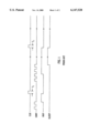
- FIG. 1 is a timing diagram for a prior art system using two pins to implement a sleep mode
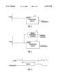
- FIG. 2 is a schematic diagram of a power down circuit according to a preferred embodiment of the present invention.
- FIG. 3 is an augmentation of the circuit of FIG. 2, showing an arrangement in which a clock-responsive means is connected upstream of the monostable of FIG. 2, and
- FIG. 4 is a timing diagram for the preferred embodiment of the invention as shown in FIG. 2 or FIG. 3.
- FIG. 1 shows a known method to power down an electronic system including an integrated circuit.
- the chip in this case an LTC 1400, as manufactured by Linear Technology Corporation, may be powered down to one of two modes: nap and sleep.
- nap and sleep For ⁇ nap ⁇ mode, the CLK pin is kept low and the CONV pin is pulsed twice.
- ⁇ sleep ⁇ mode the CLK pin is kept low and the CONV pin pulsed four times.
- the CLK pin is pulsed. It will be apparent from FIG. 1 that two pins are therefore required for powering down the chip.
- the functionality of pins on an integrated circuit varies with application, examples including a positive supply voltage, a ground reference, a reference voltage, an output pin and an input pin.
- FIG. 2 shows a preferred embodiment of a circuit in accordance with the invention.
- the CLKIN pin is held low for a period longer than the normal clock low interval to invoke a powerdown.
- a monostable timing circuit 2 is connected to the CLKIN pin.
- the monostable detects the presence of a clocking signal and generates an active output some time period t delay after its reset line is released, unless another reset occurs.
- the reset of the monostable 2 is connected to the CLKIN pin. As long as the edges on the CLKIN pin occur with a period less than t delay , the monostable 2 will be reset before its output can go high. Monostable 2 hence remains inactive under these conditions.
- the monostable output becomes active, forcing a powerdown.
- the monostable circuit 2 itself is not powered down, as it must remain in control of the power status.
- the output signal from the monostable 2 remains active until a rising transition on CLKIN forces a reset of the monostable, and thus deactivates the powerdown signal.
- FIG. 3 illustrates an alternative manner in which the active output or primary function of the circuit embodying the powerdown feature according to the present invention may be implemented.
- means 3 responsive to the clock signal is connected to the input to the monostable 2 upstream of the monostable.
- Means 3 is active in the presence of the clock signal to implement the primary function or active output of the circuit.
- FIG. 4 A timing diagram is shown in FIG. 4 and illustrates the relationship between the CLKIN signal and the powerdown signal for the embodiments of any of FIGS. 2 and 3.
- a powerdown is implemented if no rising edge pulse from the CLKIN is detected within a period less than t delay . As detailed above, a rising transition on the CLKIN pin forces a reset of the monostable 2, thus deactivating the powerdown signal.
- the embodiment outlined above utilizes a shared functionality with the CLKIN pin to invoke a power down mode.
- Any other input pin which changes state with predictable regularity during normal operation could also be used, i.e. any pin to which a normally repeating or changing cyclic signal such as a clock or synchronizing pulse is applied.
- the pin is held in a constant state for a period longer than the longest constant period which occurs in normal operation. This extended constant state status is detected and invokes the powerdown mode. Resuming toggling of the pin reverses conditions and removes operation from the powerdown mode.
- the pin may be held in either the high or a low state to establish powerdown, but in the preferred embodiment the low state is used, because in situations of supply fluctuation, (e.g.
- a logic low state is easier to detect reliably than a logic high state.
- the detection circuitry is not restricted to a monostable, as any other circuit capable of differentiating between the timing of normal operation signals and signals implemented for a specific purpose may also be used.
- the signal generated by monostable 2 is used to invoke a powerdown mode, but it could be equally used to invoke a reset mode, a test mode or any other secondary function not requiring normal operation of the circuit.
- the signal generated according to the invention may also be made available as a pin or lead of the package for use in electrical circuitry outside the package.
- the present invention is based on the fact that the clock need not be present during power-down. Operating on a binary logic principle, the present invention is easier to implement than methods requiring ternary logic states.
- the present invention requires only the addition of a simple timer circuit. In comparison with the methods involving dual pin interaction, the present invention represents a significant improvement in that no special signal sequences are required. Only one pin is used, rather than the two pins of certain prior art arrangements, thus simplifying the applications circuit, especially if the device in question is being operated remotely from the remainder of the circuit. With an internal timer circuit pre-implemented on the integrated circuit, the user requirement is merely to pull the clock low, for example by addition of an external logic gate, such as an AND or OR gate.
Abstract
Description
Claims (20)
Priority Applications (1)
| Application Number | Priority Date | Filing Date | Title |
|---|---|---|---|
| US09/041,937 US6147528A (en) | 1998-03-13 | 1998-03-13 | Method of invoking a power-down mode on an integrated circuit by monitoring a normally changing input signal |
Applications Claiming Priority (1)
| Application Number | Priority Date | Filing Date | Title |
|---|---|---|---|
| US09/041,937 US6147528A (en) | 1998-03-13 | 1998-03-13 | Method of invoking a power-down mode on an integrated circuit by monitoring a normally changing input signal |
Publications (1)
| Publication Number | Publication Date |
|---|---|
| US6147528A true US6147528A (en) | 2000-11-14 |
Family
ID=21919145
Family Applications (1)
| Application Number | Title | Priority Date | Filing Date |
|---|---|---|---|
| US09/041,937 Expired - Lifetime US6147528A (en) | 1998-03-13 | 1998-03-13 | Method of invoking a power-down mode on an integrated circuit by monitoring a normally changing input signal |
Country Status (1)
| Country | Link |
|---|---|
| US (1) | US6147528A (en) |
Cited By (2)
| Publication number | Priority date | Publication date | Assignee | Title |
|---|---|---|---|---|
| US6552578B1 (en) * | 2002-06-10 | 2003-04-22 | Pericom Semiconductor Corp. | Power down circuit detecting duty cycle of input signal |
| US20040164888A1 (en) * | 1999-08-16 | 2004-08-26 | Christian Eichrodt | System and method for implementing a delta-sigma modulator integrity supervisor |
Citations (10)
| Publication number | Priority date | Publication date | Assignee | Title |
|---|---|---|---|---|
| US4350975A (en) * | 1980-07-18 | 1982-09-21 | American Microsystems, Inc. | Dual bandwidth autozero loop for a voice frequency CODEC |
| US4434403A (en) * | 1981-08-24 | 1984-02-28 | Burroughs Corporation | Universal reset circuit for digital circuitry |
| US4528629A (en) * | 1981-05-14 | 1985-07-09 | Robert Bosch Gmbh | Electronic control apparatus with defined reset function |
| US4737723A (en) * | 1985-05-27 | 1988-04-12 | Canon Kabushiki Kaisha | Drop-out detection circuit |
| US4847782A (en) * | 1986-09-23 | 1989-07-11 | Associated Data Consultants, Inc. | Energy management system with responder unit having an override |
| US5350411A (en) * | 1993-06-28 | 1994-09-27 | Medtronic, Inc. | Pacemaker telemetry system |
| US5523708A (en) * | 1993-09-14 | 1996-06-04 | Fujitsu Limited | Apparatus for monitoring abnormality of each clock driver input and output signal in a circuit comprising a plurality of clock drivers |
| US5619204A (en) * | 1995-02-27 | 1997-04-08 | Analog Devices, Incorporated | Analog-to-digital converter with optional low-power mode |
| US5714955A (en) * | 1995-06-07 | 1998-02-03 | Linear Technology Corporation | Analog-to-digital converter |
| US5739708A (en) * | 1995-09-19 | 1998-04-14 | Siemens Aktiengesellschaft | Circuit configuration for generating an enable signal for a clock-controllable circuit |
-
1998
- 1998-03-13 US US09/041,937 patent/US6147528A/en not_active Expired - Lifetime
Patent Citations (10)
| Publication number | Priority date | Publication date | Assignee | Title |
|---|---|---|---|---|
| US4350975A (en) * | 1980-07-18 | 1982-09-21 | American Microsystems, Inc. | Dual bandwidth autozero loop for a voice frequency CODEC |
| US4528629A (en) * | 1981-05-14 | 1985-07-09 | Robert Bosch Gmbh | Electronic control apparatus with defined reset function |
| US4434403A (en) * | 1981-08-24 | 1984-02-28 | Burroughs Corporation | Universal reset circuit for digital circuitry |
| US4737723A (en) * | 1985-05-27 | 1988-04-12 | Canon Kabushiki Kaisha | Drop-out detection circuit |
| US4847782A (en) * | 1986-09-23 | 1989-07-11 | Associated Data Consultants, Inc. | Energy management system with responder unit having an override |
| US5350411A (en) * | 1993-06-28 | 1994-09-27 | Medtronic, Inc. | Pacemaker telemetry system |
| US5523708A (en) * | 1993-09-14 | 1996-06-04 | Fujitsu Limited | Apparatus for monitoring abnormality of each clock driver input and output signal in a circuit comprising a plurality of clock drivers |
| US5619204A (en) * | 1995-02-27 | 1997-04-08 | Analog Devices, Incorporated | Analog-to-digital converter with optional low-power mode |
| US5714955A (en) * | 1995-06-07 | 1998-02-03 | Linear Technology Corporation | Analog-to-digital converter |
| US5739708A (en) * | 1995-09-19 | 1998-04-14 | Siemens Aktiengesellschaft | Circuit configuration for generating an enable signal for a clock-controllable circuit |
Non-Patent Citations (6)
| Title |
|---|
| "+3.OV to +5.5V, 1 uA, up to 250kbps, True RS-232 Transceiver with AutoShutdown Plus", (MAX3238), Maxim, Sept., 1996. |
| "Complete SO-8, 12-Bit, 400ksps ADC with Shutdown", (LTC 1400), Linear Technology, May 1996. |
| "Single/Dual, +3V/+5V Dual-Speed Comparators with Auto-Standby", (MAX975/MAX977), Maxim, Sept., 1996. |
| 3.OV to 5.5V, 1 uA, up to 250kbps, True RS 232 Transceiver with AutoShutdown Plus , (MAX3238), Maxim, Sept., 1996. * |
| Complete SO 8, 12 Bit, 400ksps ADC with Shutdown , (LTC 1400), Linear Technology, May 1996. * |
| Single/Dual, 3V/ 5V Dual Speed Comparators with Auto Standby , (MAX975/MAX977), Maxim, Sept., 1996. * |
Cited By (3)
| Publication number | Priority date | Publication date | Assignee | Title |
|---|---|---|---|---|
| US20040164888A1 (en) * | 1999-08-16 | 2004-08-26 | Christian Eichrodt | System and method for implementing a delta-sigma modulator integrity supervisor |
| US7555036B2 (en) * | 1999-08-16 | 2009-06-30 | Brooktree Broadband Holding, Inc. | System and method for implementing a delta-sigma modulator integrity supervisor |
| US6552578B1 (en) * | 2002-06-10 | 2003-04-22 | Pericom Semiconductor Corp. | Power down circuit detecting duty cycle of input signal |
Similar Documents
| Publication | Publication Date | Title |
|---|---|---|
| US10514747B2 (en) | Low-power communication apparatus with wakeup detection and associated methods | |
| US7937600B1 (en) | Low power mode for a network interface | |
| US6567921B1 (en) | Asynchronous low power mode bus controller circuit and method of low power mode operation | |
| US6586963B2 (en) | Integrated circuit devices having power control logic that inhibits internal leakage current loss during sleep mode operation and method of operating same | |
| US4686386A (en) | Power-down circuits for dynamic MOS integrated circuits | |
| AU2009291819B2 (en) | Circuit having a low power mode | |
| US5623234A (en) | Clock system | |
| KR100379766B1 (en) | Pll system clock generator with instantaneous clock frequency shifting | |
| US20080276114A1 (en) | Micro-controller having USB control unit, MC unit and oscillating circuit commonly used by the USB control unit and the MC unit | |
| KR100322649B1 (en) | Low power high precision clock circuit and integrated circuit clocking method | |
| US20050041360A1 (en) | Systems and methods for achieving low power standby through interaction between a microcontroller and a switching mode power supply | |
| EP1749256B1 (en) | Automatic clock speed control | |
| US5903601A (en) | Power reduction for UART applications in standby mode | |
| EP0604044B1 (en) | Power supply loss sensor | |
| KR100295042B1 (en) | Synchronous DRAM semiconductor device with stand-by current reduction function | |
| US5867718A (en) | Method and apparatus for waking up a computer system via a parallel port | |
| US5418485A (en) | Clock signal conditioning circuit | |
| EP0549165A2 (en) | Power conserving integrated circuit | |
| US6147528A (en) | Method of invoking a power-down mode on an integrated circuit by monitoring a normally changing input signal | |
| CN111427441B (en) | Power supply awakening method and device | |
| EP0277767B1 (en) | Dynamic cmos current surge control | |
| US7952401B2 (en) | Standby control circuit and method | |
| US5799177A (en) | Automatic external clock detect and source select circuit | |
| US5587675A (en) | Multiclock controller | |
| JP2870337B2 (en) | Communication device |
Legal Events
| Date | Code | Title | Description |
|---|---|---|---|
| AS | Assignment |
Owner name: ANALOG DEVICES, INC., MASSACHUSETTS Free format text: ASSIGNMENT OF ASSIGNORS INTEREST;ASSIGNORS:O'DOWD, JOHN;WYNNE, JOHN;REEL/FRAME:009268/0815 Effective date: 19980511 |
|
| FEPP | Fee payment procedure |
Free format text: PAYOR NUMBER ASSIGNED (ORIGINAL EVENT CODE: ASPN); ENTITY STATUS OF PATENT OWNER: LARGE ENTITY |
|
| STCF | Information on status: patent grant |
Free format text: PATENTED CASE |
|
| FEPP | Fee payment procedure |
Free format text: PAYER NUMBER DE-ASSIGNED (ORIGINAL EVENT CODE: RMPN); ENTITY STATUS OF PATENT OWNER: LARGE ENTITY Free format text: PAYOR NUMBER ASSIGNED (ORIGINAL EVENT CODE: ASPN); ENTITY STATUS OF PATENT OWNER: LARGE ENTITY |
|
| FEPP | Fee payment procedure |
Free format text: PAYER NUMBER DE-ASSIGNED (ORIGINAL EVENT CODE: RMPN); ENTITY STATUS OF PATENT OWNER: LARGE ENTITY Free format text: PAYOR NUMBER ASSIGNED (ORIGINAL EVENT CODE: ASPN); ENTITY STATUS OF PATENT OWNER: LARGE ENTITY |
|
| FEPP | Fee payment procedure |
Free format text: PAYER NUMBER DE-ASSIGNED (ORIGINAL EVENT CODE: RMPN); ENTITY STATUS OF PATENT OWNER: LARGE ENTITY Free format text: PAYOR NUMBER ASSIGNED (ORIGINAL EVENT CODE: ASPN); ENTITY STATUS OF PATENT OWNER: LARGE ENTITY |
|
| FPAY | Fee payment |
Year of fee payment: 4 |
|
| FPAY | Fee payment |
Year of fee payment: 8 |
|
| FPAY | Fee payment |
Year of fee payment: 12 |