US6147541A - Monolithic MOS-SC circuit - Google Patents
Monolithic MOS-SC circuit Download PDFInfo
- Publication number
- US6147541A US6147541A US08/935,870 US93587097A US6147541A US 6147541 A US6147541 A US 6147541A US 93587097 A US93587097 A US 93587097A US 6147541 A US6147541 A US 6147541A
- Authority
- US
- United States
- Prior art keywords
- oscillator
- current
- capacitor
- transistor
- channel transistor
- Prior art date
- Legal status (The legal status is an assumption and is not a legal conclusion. Google has not performed a legal analysis and makes no representation as to the accuracy of the status listed.)
- Expired - Lifetime
Links
Images
Classifications
-
- H—ELECTRICITY
- H03—ELECTRONIC CIRCUITRY
- H03K—PULSE TECHNIQUE
- H03K3/00—Circuits for generating electric pulses; Monostable, bistable or multistable circuits
- H03K3/02—Generators characterised by the type of circuit or by the means used for producing pulses
- H03K3/023—Generators characterised by the type of circuit or by the means used for producing pulses by the use of differential amplifiers or comparators, with internal or external positive feedback
- H03K3/0231—Astable circuits
Definitions
- the invention relates to a switched-capacitor circuit which is monolithically integrated by means of enhancement-mode insulated-gate field-effect transistors, abbreviated to MOS-SC circuit below, which is therefore realized on and in a semiconductor chip.
- MOS-SC circuit enhancement-mode insulated-gate field-effect transistors
- an on-chip clock oscillator for generating a clock signal or an RC clock oscillator whose frequency is determined by a oscillator resistor and an oscillator capacitor,
- MOS-SC circuits having the two abovementioned types of clock oscillators, their frequency and/or their frequency stability are not so critical.
- Such MOS-SC circuits are, for example, SC analog/digital converters or SC digital/analog converters or the circuit described U.S. application Ser. No. 08/342,218 of Nov. 18, 1994.
- the settling time of operational amplifiers must, on the one hand, be short enough that the error caused by the settling time is sufficiently small, for example amounts to 0.1%, on the other hand the settling time must not be so short that the power requirement is greater than necessary and the noise sensitivity is increased owing to the increase in the noise bandwidth.
- the concrete settling time of a manufactured operational amplifier is determined by the actually realized value of the resistance which defines its quiescent current, or by the actually realized value of the current of the constant-current source; for this the production tolerance in each case lies in the region of 20%.
- the concrete transconductance of the individual transistors essentially depends on tolerances of the doping of the individual semiconductor regions, on tolerances of the thickness of silicon dioxide layers produced or deposited, that is to say present, outside the gate region, in other words the so-called field oxide, on tolerances of the gate threshold voltage and on tolerances of the channel length; for this the production tolerance lies in the region of 50%.
- the time constants of the individual switch-capacitor elements determine, together with the settling time of the respective operational amplifiers and, furthermore, together with the operating temperature and the concrete value of the operating voltage, the total settling time.
- the respective switch-capacitor-operational amplifier units must have settled within a time duration which is determined by the pulses generated by the clock oscillator.
- all of the abovementioned tolerances are effective or to be taken into account, which lie in the region of 50 % according to the above explanations.
- the tolerance of the frequency of an on-chip RC clock oscillator in this case lies in the region of 20% to 30%.
- the invention serves to solve these problems with regard to a significant reduction in the tolerance range or margin to be taken into account in the design.
- the invention consists in a switched-capacitor circuit which is monolithically integrated by means of enhancement-mode insulated-gate field-effect transistors
- an RC clock oscillator which is either an RC clock oscillator, whose frequency is determined by an oscillator resistor, which is realized as a transistor operated in the permanently current-conducting state, and an oscillator capacitor, or which is a current-controlled clock oscillator, whose frequency is determined by the quiescent current of the operational amplifier,
- the permanently current-conducting transistor is realized by a suitably biased CMOS transmission gate.
- both the resistor which determines the quiescent current of the operational amplifiers and the frequency-codetermining oscillator resistor are each realized as the ON resistance of an MOS transistor operated in the permanently current-conducting state.
- One advantage of the invention consists in the fact that the tolerance range or the margin can be brought towards 10%, since the speed of the SC circuit is tracked with the period of the clock signal.
- a resultant further advantage is a smaller noise level, since, on account of the narrower bandwidth of the operational amplifiers, the noise spectrum caused by aliasing appears to a lesser extent in frequency ranges above the frequency of the clock signal. Furthermore, the abovementioned power requirement is reduced and the clock feedthrough explained above is avoided to the largest possible extent.
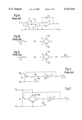
- FIGS. 1a to 1c show a circuit diagram of a simple SC circuit with the realization of conducting and non-conducting switching paths by means of CMOS transmission gates,
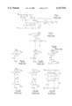
- FIG. 2 shows a basic circuit diagram of an RC oscillator
- FIG. 3 shows a circuit diagram of an RC clock oscillator according to the invention
- FIG. 4 shows a basic circuit diagram of a current-controlled clock oscillator realized using CMOS technology
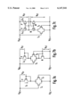
- FIG. 5 shows a basic circuit diagram of a simple differential amplifier realized using P-channel transistors
- FIGS. 6a to 6f show circuit diagrams of different simple quiescent current setting circuits of MOS or CMOS operational amplifiers
- FIGS. 7a to 7c shows circuit diagrams of different inventive quiescent current setting circuits of MOS or CMOS operational amplifiers
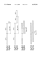
- FIGS. 8 to 11 show different margin diagrams.
- FIG. 1a shows a circuit diagram of a simple SC circuit which can also be understood as the basic circuit of extensive SC circuits on which the latter are built up.
- An input E can, on the one hand, be connected via a first switching path 1 c of a first changeover switch 1 to a first terminal of a first capacitor K 1 and, on the other hand, can be connected via a second switching path 1 o to a reference potential V ref , which may be, for example, the potential of a circuit zero-point.
- a second terminal of the first capacitor K 1 can be connected, on the one hand, via a first switching path 2 o of a second changeover switch 2 to an inverting input of an operational amplifier 3 and, on the other hand, can be connected via a second switching path 2 c to the reference potential V ref .
- a non-inverting input of the operational amplifier 3 is connected to the reference potential V ref .
- An output A of the operational amplifier 3 is connected via a second capacitor K 2 to its inverting input and can consequently also be connected to the second terminal of the first capacitor K 1 .
- the first capacitor K 1 is charged by a signal present at the input E. If the two changeover switches 1, 2 are brought to their other switch positions, the charging is interrupted or terminated and the charge which has passed to the first capacitor K 1 is forwarded to the second capacitor K 2 .
- CMOS transmission gates can serve as an example of a preferred realization of conducting and non-conducting switching paths of changeover switches of SC circuits, which CMOS transmission gates are, as is known, partial circuits of integrated CMOS circuits, that is to say of integrated circuits having complementary enhancement-mode insulated-gate field-effect transistors.
- field-effect transistors of a uniform conduction type can also be used to realize the switching paths.
- FIGS. 1b and 1c show the realization of an open and closed switching path S o and S c , respectively, by means of a CMOS transmission gate. This comprises the parallel circuit formed by the controlled current paths of a P-channel transistor T p and an N-channel transistor T n .
- a voltage V DD is present at the gate of the P-channel transistor T p and, at the same time, a voltage V SS is present at the gate of the N-channel transistor T n .
- the voltage V DD is significantly more negative than the gate threshold voltage of the P-channel transistor T p
- the voltage V SS is significantly more positive than the gate threshold voltage of the N-channel transistor T n .
- the voltage V SS is now present at the gate of the P-channel transistor T p and, at the same time, the voltage V DD is present at the gate of the N-channel transistor T n .
- the voltage V DD is now significantly more positive than the gate threshold voltage of the P-channel transistor T p
- the voltage V SS is significantly more negative than the gate threshold voltage of the P-channel transistor T n .
- the two switched-on complementary transistors consequently realize a resistor RON, which can normally have a value of the order of magnitude of 10 k ⁇ .
- FIG. 2 illustrates the basic circuit diagram of an RC oscillator.
- an oscillator changeover switch S O switches an oscillator capacitor K O back and forth between the voltages V DD and V SS .
- the junction point between the oscillator resistor W O and the oscillator capacitor K O is connected to an input of a Schmitt trigger 4, an output of which is connected to the control input of the oscillator changeover switch S O .
- a square-wave signal is thus produced at this output, the frequency of which square-wave signal is essentially determined by the time constant of the RC element formed by the resistor W O and the capacitor K O . As is known, this is equal to the product of the value R of the resistor W O and the value C of the capacitor K O .
- FIG. 3 shows a circuit diagram, which largely corresponds to the circuit diagram of FIG. 2, of an RC clock oscillator in accordance with one aspect of the invention.
- the difference from FIG. 2 consists in the fact that the resistor W O is realized by a permanently switched-on CMOS transmission gate in accordance with FIG. 1c, with the result that the following holds true for the value R of the resistor W O :R R ON .
- FIG. 4 shows a basic circuit diagram of a customary current-controlled clock oscillator which is realized using CMOS technology.
- the resistor W O according to FIGS. 2 and 3 is replaced by a CMOS current mirror.
- the latter comprises a series circuit formed by a P-channel resistor P 1 and an N-channel transistor N 1 as well as a further P-channel transistor P 2 and a further N-channel transistor N 2 .
- the controlled current paths of the P-channel transistor P 1 and of the N-channel transistor N 1 are connected in series in such a way that the drain of the P-channel transistor P 1 is connected to the voltage V DD and the source of the N-channel transistor N 1 is connected to the voltage V SS .
- the drain of the P-channel transistor P 2 is likewise connected to the voltage V DD and the source of the N-channel transistor N 2 is likewise connected to the voltage V SS .
- the gates of the two N-channel transistors N 1 , N 2 are connected to one another and, furthermore, are connected to the junction point between the two transistors of the series circuit, that is to say to the drain of the N-channel transistor N 1 and to the source of the P-channel transistor P 1 .
- the respective gate of the two P-channel transistors P 1 , P 2 is also connected to this junction point.
- the source of the further P-channel transistor P 2 is connected to a first input of the changeover switch S O and the drain of the further N-channel transistor N 2 is connected to a second input of the changeover switch S O .
- the output of the latter is connected, as in FIG. 3, to the input of the Schmitt trigger 4 and to the capacitor K O .
- this quiescent current I O thus also flows in the further P-channel transistor P 2 if, as is depicted in FIG. 4, the changeover switch S O is in the position depicted, and consequently charges the capacitor K O .
- FIG. 5 shows a basic circuit diagram of a simple differential amplifier, which is realized using P-channel transistors, as the basic element of operational amplifiers.
- the differential amplifier comprises two amplifier transistors V 1 , V 2 , the drains of which are connected to one another and are coupled to the voltage V DD via the controlled quiescent current path of a constant-current transistor V 3 .
- V b1 There is present between the gate of the latter and the voltage V DD a bias voltage V b1 , which codetermines the quiescent current I b flowing in this transistor. Consequently, in this case, too, the quiescent current I b can be set by the user by means of the bias voltage V b1 .
- a quiescent current I 1 and, respectively, I 2 flows in the amplifier transistor V 1 and in the amplifier transistor V 2 , in which case, as is characteristic of differential amplifiers, the sum of these two currents is constant and equal to the quiescent current I b :
- the quiescent current I b is divided between the two amplifier transistors V 1 , V 2 as a function of a difference between variable signals v i1 and v i2 present at the respective gate of the amplifier transistors V 1 , V 2 , with the result that variable currents i 1 , i 2 flow in them.
- These currents i 1 , i 2 are further processed in further stages of the operational amplifiers or in other stages of an integrated circuit.
- ⁇ p is a production-dictated constant.
- c is the known Miller capacitance. At all events the capacitive load c must be of the same type as the capacitors otherwise used in the SC circuit and in the clock oscillator.
- FIG. 6 shows circuit diagrams of different simple quiescent current setting circuits of MOS or CMOS operational amplifiers.
- FIG. 6a shows a P-channel transistor P, the controlled current path of which is connected in series with a resistor W between the voltage V DD and the voltage V SS , which resistor has the resistance R.
- the gate of the transistor P is connected to its junction point with the resistor W, and across this gate is a bias voltage V b1 codetermining the quiescent current I b which flows in the series circuit formed by the resistor W and the transistor P. Codetermining because the quiescent current I b also depends on the dimensioning of the channel of the transistor W, namely on the quotient w/1 (w is the width of the said channel and 1 is its length). The following holds true for the quiescent current I b :
- the resistor W of FIG. 6a is replaced by a constant-current source Q.
- the controlled current path of an N-channel transistor N is connected in series with the resistor W at the voltage V SS end.
- the gate of the transistor N is connected to its junction point with the resistor W, and across this gate is a bias voltage V b2 , which additionally codetermines the quiescent current I b flowing in the series circuit formed by the transistor P, the resistor W and the transistor N.
- V b2 bias voltage
- the resistor W of FIG. 6c is replaced by a P-channel transistor D P connected as a diode, in that the controlled current path of the said P-channel transistor D P is inserted into the series circuit formed by the P-channel transistor P and the N-channel transistor N.
- the gate of the transistor D P is connected to its junction point with the N-channel transistor N, that is to say also to the gate of the latter.
- the resistor W of FIG. 6c is replaced by an N-channel transistor D N connected as a diode, in that the controlled current path of the said N-channel transistor D N is inserted into the series circuit formed by the P-channel transistor P and the N-channel transistor N.
- the gate of the transistor D N is connected to its junction point with the P-channel transistor P, that is to say also to the gate connection of the latter.
- the respective transistor D P or DN connected as a diode usually has a small w/l ratio, in order to obtain a quiescent current setting circuit having a small power loss.
- FIG. 6f shows a quiescent current setting circuit having a very much smaller power loss. Two parallel circuit paths are formed. The quiescent current I b flows in each of them.
- a first circuit path, the left-hand one in FIG. 6 f comprises, viewed starting from the voltage V DD , the series circuit formed by the P-channel transistor P, the N-channel transistor N and the resistor W.
- a second circuit path, the right-hand one in FIG. 6f comprises, viewed starting from the voltage V DD , the series circuit formed by a further P-channel transistor P' and a further N-channel transistor N'.
- the gate of the further P-channel transistor P' is connected to the gate of the P-channel transistor P.
- the gate of the further N-channel transistor N' is connected to the gate of the N-channel transistor N and is connected to the junction point between the two further transistors.
- the connection between the gate of the N-channel transistor N and its drain, as is present in FIG. 6e, is not present.
- the N-channel transistor has an increased w/1 ratio in comparison with the respective w/1 ratio of these transistors P, P', N'; this is illustrated by the designation 1 ⁇ in the case of the transistors P, P', N'and the designation 4 ⁇ in the case of the transistor N, where 4 ⁇ is intended to indicate that the w/1 ratio of the said transistor N is four times greater than that of the transistors P, P', N'.
- the current mirror formed by the transistors P, P' ensures that the quiescent current I b in the first circuit path is identical to the quiescent current I b in the second circuit path.
- the gate-source voltage V gsN , of the transistor N' is therefore smaller than the gate-source voltage V gsN of the transistor N. Consequently, the following holds true for the quiescent current I b :
- FIGS. 7a to 7c illustrate quiescent current setting circuits comparable to FIGS. 6a, 6c and 6f, in which circuits, according to the invention, the respective resistor W is replaced by a permanently switched-on CMOS transmission gate according to FIG. 1c.
- FIGS. a) and b) of FIGS. 8 to 11 illustrate a number of bar diagrams of the margin, the latter in the sense defined above, cf. section g).
- the partial FIG. a) each relate to the necessary settling time of the MOS-SC circuit and the respective partial FIG. b) to the period of the clock signal.
- the rectangles which are not filled in represent the respective average tolerance ranges
- the hatched rectangles represent partial tolerance ranges which are correlated with one another
- the narrow filled-in rectangles represent typical values.
- FIGS. 8a and 8b show, as was already mentioned above, the average tolerance range of the required settling time of an integrated MOS operational amplifier ( ⁇ 50%) and, respectively, the tolerance range of a crystal oscillator serv-ing as a clock pulse generator.
- the resultant margin M Q in this case amounts to approximately 55%.
- FIGS. 9a and 9b show the conditions given with an integrated MOS operational amplifier (tolerance range again ⁇ 50%) and, respectively, a customary on-chip RC oscillator as clock pulse generator, when there is no correlation between their tolerance ranges.
- FIG. 9a is identical to FIG. 8a, and
- FIG. 9b shows the average tolerance range of the on-chip RC oscillator to be ⁇ 30%.
- the margin MRC in this case amounts to approximately 80%.
- FIGS. 10a and 10b show the conditions given with a customary on-chip RC oscillator as clock pulse generator when there is typical correlation between their tolerance ranges.
- FIG. 10a shows the average tolerance range of the required settling time of an integrated MOS operational amplifier of again ⁇ 50 % with a partial tolerance range of ⁇ 25%.
- the left-hand edge of the tolerance range of the on-chip RC oscillator can be shifted to the typical value of FIG. 10a. Since this tolerance range has a correlated partial tolerance range likewise of ⁇ 25%, the margin M RCk in this case amounts to only ⁇ 30%, but this is still too large.
- the total quiescent current is increased when the resistance which determines the quiescent current is increased. This can be realized, for example, by connecting more and more CMOS transmission gates in series or, for example, by increasing the respective current ratio of the current mirrors for the quiescent current.
- the setting value required for an individual MOS-SC circuit can be determined in the course of production during testing of the said circuit and be stored in a memory, for example an EEPROM or the like.
Landscapes
- Amplifiers (AREA)
Abstract
Description
I.sub.1 +I.sub.2 =I.sub.b =constant
I.sub.b ˜(V.sub.DD -V.sub.SS -V.sub.b1)/R.
I.sub.b ˜(V.sub.DD -V.sub.SS -V.sub.b1 -V.sub.b2)/R.
I.sub.b =(V.sub.gsN '-V.sub.gsN)/R.
Claims (1)
Priority Applications (1)
| Application Number | Priority Date | Filing Date | Title |
|---|---|---|---|
| US08/935,870 US6147541A (en) | 1996-10-02 | 1997-09-23 | Monolithic MOS-SC circuit |
Applications Claiming Priority (4)
| Application Number | Priority Date | Filing Date | Title |
|---|---|---|---|
| EP96115764A EP0834992B1 (en) | 1996-10-02 | 1996-10-02 | Monolithic MOS switched-capacitor circuit with on-chip oscillator |
| EP96115764 | 1996-10-02 | ||
| US2864196P | 1996-10-17 | 1996-10-17 | |
| US08/935,870 US6147541A (en) | 1996-10-02 | 1997-09-23 | Monolithic MOS-SC circuit |
Publications (1)
| Publication Number | Publication Date |
|---|---|
| US6147541A true US6147541A (en) | 2000-11-14 |
Family
ID=27237424
Family Applications (1)
| Application Number | Title | Priority Date | Filing Date |
|---|---|---|---|
| US08/935,870 Expired - Lifetime US6147541A (en) | 1996-10-02 | 1997-09-23 | Monolithic MOS-SC circuit |
Country Status (1)
| Country | Link |
|---|---|
| US (1) | US6147541A (en) |
Cited By (7)
| Publication number | Priority date | Publication date | Assignee | Title |
|---|---|---|---|---|
| US20030164739A1 (en) * | 2002-03-04 | 2003-09-04 | Lg Electronic Inc. | Oscillator for DC-DC converter |
| US20060061409A1 (en) * | 2004-09-17 | 2006-03-23 | Fujitsu Limited | Semiconductor device |
| US20080258826A1 (en) * | 2004-09-20 | 2008-10-23 | The Trustees Of Columbia University In The City Of New York | Low Voltage Operational Transconductance Amplifier Circuits |
| US20100033260A1 (en) * | 2008-08-06 | 2010-02-11 | Nec Electronics Corporation | Oscillation circuit |
| US20120188012A1 (en) * | 2011-01-24 | 2012-07-26 | Ju-Lin Huang | Operational Amplifier Device |
| US20130265093A1 (en) * | 2012-04-06 | 2013-10-10 | Freescale Semiconductor, Inc | Oscillator circuit for generating clock signal |
| US11073861B2 (en) * | 2018-01-16 | 2021-07-27 | Rezonent Microchips Pvt. Ltd. | Digital circuits for radically reduced power and improved timing performance on advanced semiconductor manufacturing processes |
Citations (7)
| Publication number | Priority date | Publication date | Assignee | Title |
|---|---|---|---|---|
| US5189316A (en) * | 1990-06-14 | 1993-02-23 | Mitsubishi Denki Kabushiki Kaisha | Stepdown voltage generator having active mode and standby mode |
| US5498986A (en) * | 1994-04-29 | 1996-03-12 | Delco Electronics Corporation | Oxygen sensor interface circuit with simplified amplifier requirements |
| US5502417A (en) * | 1992-12-28 | 1996-03-26 | Nec Corporation | Input amplifier circuit |
| US5585756A (en) * | 1995-02-27 | 1996-12-17 | University Of Chicago | Gated integrator with signal baseline subtraction |
| US5604685A (en) * | 1994-11-11 | 1997-02-18 | Endress Hauser Gmbh Co | Circuit arrangement for the linearization and temperature compensation of sensor signals |
| US5619170A (en) * | 1994-04-19 | 1997-04-08 | Nec Corporation | PLL timing generator with voltage controlled oscillator |
| US5745002A (en) * | 1994-06-24 | 1998-04-28 | Sgs-Thomson Microelectronics, S.R.L. | Low voltage, switched capacitance circuit employing switched operational amplifiers with maximized voltage swing |
-
1997
- 1997-09-23 US US08/935,870 patent/US6147541A/en not_active Expired - Lifetime
Patent Citations (7)
| Publication number | Priority date | Publication date | Assignee | Title |
|---|---|---|---|---|
| US5189316A (en) * | 1990-06-14 | 1993-02-23 | Mitsubishi Denki Kabushiki Kaisha | Stepdown voltage generator having active mode and standby mode |
| US5502417A (en) * | 1992-12-28 | 1996-03-26 | Nec Corporation | Input amplifier circuit |
| US5619170A (en) * | 1994-04-19 | 1997-04-08 | Nec Corporation | PLL timing generator with voltage controlled oscillator |
| US5498986A (en) * | 1994-04-29 | 1996-03-12 | Delco Electronics Corporation | Oxygen sensor interface circuit with simplified amplifier requirements |
| US5745002A (en) * | 1994-06-24 | 1998-04-28 | Sgs-Thomson Microelectronics, S.R.L. | Low voltage, switched capacitance circuit employing switched operational amplifiers with maximized voltage swing |
| US5604685A (en) * | 1994-11-11 | 1997-02-18 | Endress Hauser Gmbh Co | Circuit arrangement for the linearization and temperature compensation of sensor signals |
| US5585756A (en) * | 1995-02-27 | 1996-12-17 | University Of Chicago | Gated integrator with signal baseline subtraction |
Non-Patent Citations (6)
| Title |
|---|
| Goodenough, Frank, Hot and Getting Hotter, These Ics are Now Software Programmable , 2328 Electronic Design, 37 Apr. 13, 1989, No. 8, Hasbrouck Heights, NJ, pp. 77 80, 86, 90, and 92. * |
| Goodenough, Frank, Hot and Getting Hotter, These Ics are Now Software Programmable, 2328 Electronic Design, 37 Apr. 13, 1989, No. 8, Hasbrouck Heights, NJ, pp. 77-80, 86, 90, and 92. |
| Hosticka, bedrich J., Brockherde, Werner, Kleine, Ulrich, and Schweer, Rainer, Design of Nonlinear Analog Switched Capacitor Circuits Using Building Blocks , 8090 IEEE Transactions on Circuits and Systems, CAS 31 (1984) Apr., No. 4, New York, NY, pp. 354 368. * |
| Hosticka, bedrich J., Brockherde, Werner, Kleine, Ulrich, and Schweer, Rainer, Design of Nonlinear Analog Switched-Capacitor Circuits Using Building Blocks, 8090 IEEE Transactions on Circuits and Systems, CAS-31 (1984) Apr., No. 4, New York, NY, pp. 354-368. |
| Mariano, Aceves M., Torres, Alfonso, Prieto, Arturo, Glaenzer, Richard, and Worley, John, Advanced Technologies and Processes in Communication and Power Systems , 7th European Conference on Electrotechnics, Apr. 21 23, 1986, Paris, France, pp. 659 664. * |
| Mariano, Aceves M., Torres, Alfonso, Prieto, Arturo, Glaenzer, Richard, and Worley, John, Advanced Technologies and Processes in Communication and Power Systems, 7th European Conference on Electrotechnics, Apr. 21-23, 1986, Paris, France, pp. 659-664. |
Cited By (17)
| Publication number | Priority date | Publication date | Assignee | Title |
|---|---|---|---|---|
| US20030164739A1 (en) * | 2002-03-04 | 2003-09-04 | Lg Electronic Inc. | Oscillator for DC-DC converter |
| US6909335B2 (en) * | 2002-03-04 | 2005-06-21 | Lg Electronics Inc. | Oscillator for DC—DC converter |
| US20060061409A1 (en) * | 2004-09-17 | 2006-03-23 | Fujitsu Limited | Semiconductor device |
| US7342434B2 (en) * | 2004-09-17 | 2008-03-11 | Fujitsu Limited | Semiconductor device including capacitor having decoupling capacity |
| US8030999B2 (en) | 2004-09-20 | 2011-10-04 | The Trustees Of Columbia University In The City Of New York | Low voltage operational transconductance amplifier circuits |
| US20090015329A1 (en) * | 2004-09-20 | 2009-01-15 | Shouri Chatterjee | Low Voltage Track and Hold Circuits |
| US20090303094A1 (en) * | 2004-09-20 | 2009-12-10 | The Trustees Of Columbia University In The City Of New York | Low voltage digital to analog converter, comparator and sigma-delta modulator circuits |
| US20080258826A1 (en) * | 2004-09-20 | 2008-10-23 | The Trustees Of Columbia University In The City Of New York | Low Voltage Operational Transconductance Amplifier Circuits |
| US8305247B2 (en) | 2004-09-20 | 2012-11-06 | The Trustees Of Columbia University In The City Of New York | Low voltage digital to analog converter, comparator and sigma-delta modulator circuits |
| US8441287B2 (en) * | 2004-09-20 | 2013-05-14 | The Trustees Of Columbia University In The City Of New York | Low voltage track and hold circuits |
| US8704553B2 (en) | 2004-09-20 | 2014-04-22 | The Trustees Of Columbia University In The City Of New York | Low voltage comparator circuits |
| US20100033260A1 (en) * | 2008-08-06 | 2010-02-11 | Nec Electronics Corporation | Oscillation circuit |
| US20120188012A1 (en) * | 2011-01-24 | 2012-07-26 | Ju-Lin Huang | Operational Amplifier Device |
| US8344802B2 (en) * | 2011-01-24 | 2013-01-01 | Novatek Microelectronics Corp. | Operational amplifier device |
| US20130265093A1 (en) * | 2012-04-06 | 2013-10-10 | Freescale Semiconductor, Inc | Oscillator circuit for generating clock signal |
| US8830006B2 (en) * | 2012-04-06 | 2014-09-09 | Freescale Semiconductor, Inc. | Oscillator circuit for generating clock signal |
| US11073861B2 (en) * | 2018-01-16 | 2021-07-27 | Rezonent Microchips Pvt. Ltd. | Digital circuits for radically reduced power and improved timing performance on advanced semiconductor manufacturing processes |
Similar Documents
| Publication | Publication Date | Title |
|---|---|---|
| US4622480A (en) | Switched capacitor circuit with high power supply projection ratio | |
| KR100271633B1 (en) | Delay circuit | |
| US4464588A (en) | Temperature stable CMOS voltage reference | |
| US5045806A (en) | Offset compensated amplifier | |
| US5281906A (en) | Tunable voltage reference circuit to provide an output voltage with a predetermined temperature coefficient independent of variation in supply voltage | |
| US5235218A (en) | Switching constant current source circuit | |
| US6147541A (en) | Monolithic MOS-SC circuit | |
| JPH05175811A (en) | Power-on reset circuit | |
| US4460874A (en) | Three-terminal operational amplifier/comparator with offset compensation | |
| CA2216725C (en) | Monolithic mos-sc circuit | |
| US5221910A (en) | Single-pin amplifier in integrated circuit form | |
| US4550295A (en) | Switched capacitor integrator | |
| US4431929A (en) | CMOS Dynamic amplifier | |
| US5767708A (en) | Current integrator circuit with conversion of an input current into a capacitive charging current | |
| US5136293A (en) | Differential current source type d/a converter | |
| EP0868026B1 (en) | Variable delay circuit | |
| JP2981279B2 (en) | I / O circuit | |
| JP3047828B2 (en) | Comparator circuit | |
| US4616172A (en) | Voltage generator for telecommunication amplifier | |
| JPH11234088A (en) | Switched capacitor circuit | |
| US20040145389A1 (en) | High speed current mode NOR logic circuit | |
| US20020130706A1 (en) | Integrated circuit current source with switched capacitor feedback | |
| EP0499645A1 (en) | Differential amplifying circuit of operational amplifier | |
| JP2901608B2 (en) | Ring oscillation circuit | |
| JPH0239607A (en) | Semiconductor integrated circuit device |
Legal Events
| Date | Code | Title | Description |
|---|---|---|---|
| AS | Assignment |
Owner name: ENDRESS + HAUSER GMBH + CO., GERMANY Free format text: ASSIGNMENT OF ASSIGNORS INTEREST;ASSIGNOR:SEESINK, PETRUS H.;REEL/FRAME:009598/0246 Effective date: 19981007 Owner name: KAVLICO CORPORATION, CALIFORNIA Free format text: ASSIGNMENT OF ASSIGNORS INTEREST;ASSIGNOR:SEESINK, PETRUS H.;REEL/FRAME:009598/0246 Effective date: 19981007 Owner name: ENVEC MESS-UND REGELTECHNIK GMBH + CO., GERMANY Free format text: ASSIGNMENT OF ASSIGNORS INTEREST;ASSIGNOR:SEESINK, PETRUS H.;REEL/FRAME:009598/0246 Effective date: 19981007 Owner name: VEGA GRIESHABER KG, GERMANY Free format text: ASSIGNMENT OF ASSIGNORS INTEREST;ASSIGNOR:SEESINK, PETRUS H.;REEL/FRAME:009598/0246 Effective date: 19981007 |
|
| STCF | Information on status: patent grant |
Free format text: PATENTED CASE |
|
| REMI | Maintenance fee reminder mailed | ||
| FPAY | Fee payment |
Year of fee payment: 4 |
|
| SULP | Surcharge for late payment | ||
| FEPP | Fee payment procedure |
Free format text: PAYOR NUMBER ASSIGNED (ORIGINAL EVENT CODE: ASPN); ENTITY STATUS OF PATENT OWNER: LARGE ENTITY |
|
| FPAY | Fee payment |
Year of fee payment: 8 |
|
| FPAY | Fee payment |
Year of fee payment: 12 |
|
| AS | Assignment |
Owner name: DEUTSCHE BANK AG NEW YORK BRANCH, AS COLLATERAL AG Free format text: SECURITY AGREEMENT;ASSIGNORS:BEI SENSORS & SYSTEMS COMPANY, INC.;CUSTOM SENSORS & TECHNOLOGIES, INC;CRYDOM, INC.;AND OTHERS;REEL/FRAME:033888/0700 Effective date: 20140930 |
|
| AS | Assignment |
Owner name: CRYDOM, INC., CALIFORNIA Free format text: RELEASE BY SECURED PARTY;ASSIGNOR:DEUTSCHE BANK AG NEW YORK BRANCH;REEL/FRAME:037196/0174 Effective date: 20151201 Owner name: KAVLICO CORPORATION, CALIFORNIA Free format text: RELEASE BY SECURED PARTY;ASSIGNOR:DEUTSCHE BANK AG NEW YORK BRANCH;REEL/FRAME:037196/0174 Effective date: 20151201 Owner name: BEI TECHNOLOGIES, INC., CALIFORNIA Free format text: RELEASE BY SECURED PARTY;ASSIGNOR:DEUTSCHE BANK AG NEW YORK BRANCH;REEL/FRAME:037196/0174 Effective date: 20151201 Owner name: CUSTOM SENSORS & TECHNOLOGIES, INC., CALIFORNIA Free format text: RELEASE BY SECURED PARTY;ASSIGNOR:DEUTSCHE BANK AG NEW YORK BRANCH;REEL/FRAME:037196/0174 Effective date: 20151201 Owner name: BEI SENSORS & SYSTEMS COMPANY, INC., CALIFORNIA Free format text: RELEASE BY SECURED PARTY;ASSIGNOR:DEUTSCHE BANK AG NEW YORK BRANCH;REEL/FRAME:037196/0174 Effective date: 20151201 |
|
| AS | Assignment |
Owner name: MORGAN STANLEY SENIOR FUNDING, INC., NEW YORK Free format text: SECURITY INTEREST;ASSIGNORS:BEI NORTH AMERICA LLC;CRYDOM, INC.;CUSTOM SENSORS & TECHNOLOGIES, INC.;AND OTHERS;REEL/FRAME:037927/0605 Effective date: 20160224 |