US6147846A - Drive circuit with over-voltage protection for use with pixel cells and other circuits - Google Patents
Drive circuit with over-voltage protection for use with pixel cells and other circuits Download PDFInfo
- Publication number
- US6147846A US6147846A US09/203,789 US20378998A US6147846A US 6147846 A US6147846 A US 6147846A US 20378998 A US20378998 A US 20378998A US 6147846 A US6147846 A US 6147846A
- Authority
- US
- United States
- Prior art keywords
- voltage
- over
- circuit
- transistor
- voltage signal
- Prior art date
- Legal status (The legal status is an assumption and is not a legal conclusion. Google has not performed a legal analysis and makes no representation as to the accuracy of the status listed.)
- Expired - Lifetime
Links
- 238000000034 method Methods 0.000 claims abstract description 9
- 230000008569 process Effects 0.000 claims abstract description 8
- 239000003990 capacitor Substances 0.000 claims description 8
- 239000000872 buffer Substances 0.000 claims description 6
- 239000000758 substrate Substances 0.000 claims 5
- 239000004065 semiconductor Substances 0.000 claims 3
- 230000000153 supplemental effect Effects 0.000 claims 2
- 239000004020 conductor Substances 0.000 claims 1
- 238000010586 diagram Methods 0.000 description 14
- 230000003071 parasitic effect Effects 0.000 description 6
- 230000008901 benefit Effects 0.000 description 5
- 238000013461 design Methods 0.000 description 4
- 238000005516 engineering process Methods 0.000 description 3
- 238000013459 approach Methods 0.000 description 2
- 230000009286 beneficial effect Effects 0.000 description 2
- 230000005540 biological transmission Effects 0.000 description 2
- 239000002800 charge carrier Substances 0.000 description 2
- 230000000295 complement effect Effects 0.000 description 2
- 230000000644 propagated effect Effects 0.000 description 2
- 238000012546 transfer Methods 0.000 description 2
- 230000009471 action Effects 0.000 description 1
- 230000006978 adaptation Effects 0.000 description 1
- 230000001419 dependent effect Effects 0.000 description 1
- 230000000694 effects Effects 0.000 description 1
- 230000005669 field effect Effects 0.000 description 1
- 230000006870 function Effects 0.000 description 1
- 238000003384 imaging method Methods 0.000 description 1
- 230000006872 improvement Effects 0.000 description 1
- 230000004048 modification Effects 0.000 description 1
- 238000012986 modification Methods 0.000 description 1
- 230000001902 propagating effect Effects 0.000 description 1
- 230000004044 response Effects 0.000 description 1
- 238000012552 review Methods 0.000 description 1
- 230000035945 sensitivity Effects 0.000 description 1
- 230000008054 signal transmission Effects 0.000 description 1
- 230000007704 transition Effects 0.000 description 1
Images
Classifications
-
- H—ELECTRICITY
- H03—ELECTRONIC CIRCUITRY
- H03K—PULSE TECHNIQUE
- H03K17/00—Electronic switching or gating, i.e. not by contact-making and –breaking
- H03K17/16—Modifications for eliminating interference voltages or currents
-
- H—ELECTRICITY
- H04—ELECTRIC COMMUNICATION TECHNIQUE
- H04N—PICTORIAL COMMUNICATION, e.g. TELEVISION
- H04N25/00—Circuitry of solid-state image sensors [SSIS]; Control thereof
- H04N25/60—Noise processing, e.g. detecting, correcting, reducing or removing noise
- H04N25/62—Detection or reduction of noise due to excess charges produced by the exposure, e.g. smear, blooming, ghost image, crosstalk or leakage between pixels
- H04N25/626—Reduction of noise due to residual charges remaining after image readout, e.g. to remove ghost images or afterimages
-
- H—ELECTRICITY
- H04—ELECTRIC COMMUNICATION TECHNIQUE
- H04N—PICTORIAL COMMUNICATION, e.g. TELEVISION
- H04N25/00—Circuitry of solid-state image sensors [SSIS]; Control thereof
- H04N25/50—Control of the SSIS exposure
- H04N25/57—Control of the dynamic range
-
- H—ELECTRICITY
- H04—ELECTRIC COMMUNICATION TECHNIQUE
- H04N—PICTORIAL COMMUNICATION, e.g. TELEVISION
- H04N25/00—Circuitry of solid-state image sensors [SSIS]; Control thereof
- H04N25/70—SSIS architectures; Circuits associated therewith
- H04N25/71—Charge-coupled device [CCD] sensors; Charge-transfer registers specially adapted for CCD sensors
- H04N25/74—Circuitry for scanning or addressing the pixel array
-
- H—ELECTRICITY
- H04—ELECTRIC COMMUNICATION TECHNIQUE
- H04N—PICTORIAL COMMUNICATION, e.g. TELEVISION
- H04N25/00—Circuitry of solid-state image sensors [SSIS]; Control thereof
- H04N25/70—SSIS architectures; Circuits associated therewith
- H04N25/76—Addressed sensors, e.g. MOS or CMOS sensors
Definitions
- the present invention relates to drive circuits and, more specifically, to drive circuits with over-voltage protection that provide a voltage greater than a supply voltage. Such circuits are beneficial for pixel cells as discussed herein and for other uses where a greater than V DD (or V CC ) voltage is desired.
- a typical drive circuit consists of a conventional buffer that is capable of propagating to a pixel cell or other circuit a voltage level that is no higher than a logic high voltage level. In CMOS circuits this voltage high level is often V DD . As discussed in more detail below, this limitation is disadvantageous in use with pixel cells and other types of circuits.
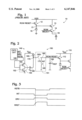
- Cell 10 includes three transistors 12-14 (which are typically n-type field-effect transistors) and a light sensitive or "photo" diode 15.
- Transistors 12 and 13 are coupled to V DD and transistor 14 is coupled to the source of transistor 13.
- a row reset signal is applied to the gate of transistor 12 and a row select signal is applied to the gate of transistor 14.
- the row reset line is asserted high to charge the parasitic capacitance of the reversed biased photo diode to a reset level. After diode output node 17 has stabilized, the row reset is pulled low, allowing photo induced charge carriers to discharge the photo diode at a rate proportional to the incident light intensity.
- the row select line is asserted high allowing the voltage at node 17 to be sampled at the cell output node 19 (normally coupled to a column of pixel cell outputs), through source follower buffer transistor 13.
- the row reset signal is again asserted high and low to reset node 17 a second time.
- the reset level is sampled at output 19. The difference between the voltage level at output 19 after exposure to incident light and at a reset level is proportional to the incident light intensity.
- the row reset signal is driven by a digital gate that limits the high level of row reset to V DD as this is typically the highest available supply voltage on a CMOS integrated circuit. While beneficial for some purposes, the use in a typical pixel cell of a row reset signal with a high level limited to V DD has disadvantageous aspects.
- V DD the dynamic range at output 19 is limited to a maximum of V DD -(2 ⁇ the NMOS threshold, Vtn).
- Vtn the NMOS threshold
- One Vtn is lost at transistor 12 and the other is lost at transistor 13.
- dynamic range for a 3.3V V DD cell is approximately 3.3-(2 ⁇ 0.8) or 1.7 to 0.4 (the turn-off voltage of a current source transistor coupled to pixel column output 19). This results in a typical dynamic range magnitude of 1.3V.
- the row reset signal must be held high for a relatively long time, on the order of 100 microseconds, before node 17 reaches its final settled voltage due to sub-threshold leakage currents at transistor 12 as that transistor approaches its cutoff state. Due to timing constraints, imaging systems may be forced to use a shorter reset interval. Shorter reset intervals can in turn result in a difference between the "before exposure” reset and the "after exposure” reset signal strengths. The net effect is a memory of the previous captured image which can either add to or subtract from the present captured image, giving the appearance of a positive or negative ghost image superimposed on the desired image.
- a first advantage of a higher row reset signal or gate voltage is that it allows the photo diode cathode (node 17) to be reset all the way to V DD without altering the pixel design, thus increasing the dynamic range of the cell by Vtn. This can be a dynamic range improvement approaching a factor of 2, depending on supply voltage level and process specifics like threshold dependence on back bias.
- a second advantage is that since the cell reset transistor never approaches cutoff during reset, the diode output node charges to the reset level much faster.
- a third advantage is that because node 17 resets all the way to V DD , the final reset level is not dependent upon the discharge level of the photo diode prior to the reset operation, thereby eliminating the occurrence of ghost images.
- An additional advantage is that the higher reset level results in a stronger reverse bias on the photo diode, resulting in smaller parasitic depletion capacitance.
- the smaller capacitance results in higher sensitivity to photo generated charge carriers and potentially improves image quality in low lighting conditions.
- the drive circuit of the present invention may be used in any application where the designer desires to use a non-complementary transmission gate for gating signals with large dynamic range.
- the gate of an n-channel MOS device can be driven by a similar drive circuit to allow it to control transmission of signals approaching the positive supply.
- Such a function would otherwise require use of a p-channel MOS device in parallel with the n-channel device, with a complementary gating signal.
- Other possible applications for the drive circuit of the present invention include use in: (1) pad circuits which must interface with higher voltage technologies, (2) FPGA, (3) fuse circuits, (4) DRAM, (5) EEPROM, and (6) flash memory.
- FIG. 1 is a block diagram of a typical photosensitive or pixel cell of the type used in an active pixel sensor device, such as a digital camera or scanner or the like.
- FIG. 2 is a diagram of a drive circuit and the pixel of FIG. 1 with which it may be used in accordance with the present invention.
- FIG. 3 is a timing diagram that illustrates operation of driver circuit 150 of FIG. 2 in accordance with the present invention.
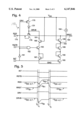
- FIG. 4 is a schematic diagram that illustrates over-voltage protection circuitry for components of drive circuit 150 of FIG. 2 in accordance with the present invention.
- FIG. 5 is a timing diagram of a single row of an active pixel sensor array in accordance with the present invention.
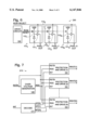
- FIG. 6 is a schematic diagram of a representative active pixel sensor array utilizing the drive circuit of FIGS. 2 and 4 in accordance with the present invention.
- FIG. 7 is a schematic diagram of a circuit for generating a plurality of over-voltage drive signals in accordance with the present invention.
- Circuit 150 achieves a row reset signal that is increased in magnitude such that the dynamic range and response time of cell 110 are improved.
- Circuit 150 essentially comprises an over-voltage generation component 149 and an over-voltage protection and drive component 151.
- Circuit 150 includes a CMOS inverter 152 that comprises PMOS transistor 153 and NMOS transistor 154.
- the inverter is coupled between V DD and ground and its output is coupled through capacitor 160 to node 170.
- Node 170 is also coupled through diode 165 to V DD and through switch 175 to the row reset signal line 180 that is in turn coupled to the gate of transistor 112 of cell 110 (which is analogous to transistor 12 of cell 10 of FIG. 1).
- An interrupt switch 185 and a capacitor 195 are shown coupled between the row reset signal line and ground.
- FIG. 3 a timing diagram that illustrates operation of driver circuit 150 of FIG. 2 in accordance with the present invention is shown.
- the drive capacitor 160 Prior to a reset operation (defined by the transition from low to high and back to low again of the row reset signal), the drive capacitor 160 is charged, DRV switch 175 is open and RSTB is high (driving the output of inverter 154 low).
- the voltage level at node 170 is settled at approximately 0.7V (one diode drop) below V DD , DRV switch 175 is open, and the INT switch is closed, holding the row reset line low.
- the INT switch 185 is then opened while the DRV switch 175 is simultaneously closed. This causes the voltage on the row reset line to rise to an equalized voltage level determined by charge transfer from drive capacitor 160 to the parasitic capacitance 188.
- the intermediate row reset voltage level equals approximately C D* (V DD -0.7)/(C RST +C D ).
- the RSTB is then asserted (driven low) which raises the output of the inverter towards V DD , which further drives the row reset signal to a level:
- Row reset is then pulled low again by opening DRV switch 175 and closing INT switch 185.
- the RSTB signal is subsequently driven high in preparation of the next row reset operation.
- the size of CD is selected relative to CRST such that the high level of Row Reset (given by Eqn. 1) is at least 1 Vtn above V DD . This way, the source of device 112 will pull up all the way to V DD during a reset interval.
- CMOS processes used to implement the above described circuit have specific limitations on maximum operating supply voltage in order to guarantee circuit reliability.
- the maximum supply voltage is typically about ten percent above an industry standard such as 5 volts or 3.3 volts. Provisions are often made, however, to interface between newer process technologies and older, higher voltage process technologies. This leads to special design rules for allowing higher voltages on an integrated circuit, typically confined to the pad rings, without compromising circuit reliability. These special design rules restrict the maximum voltage across any pair of FET device nodes to being less than the maximum rated supply voltage. Circuit design techniques should adhere to this restriction in realizing the above described circuit implementation. An exemplary circuit is now discussed.
- FIG. 4 a schematic diagram illustrating drive circuit 151 including over-voltage protection in accordance with the present invention is shown.
- Signals input to region 151 include RSTB, INT and the signal from node 170 (RSS), V DD and ground.
- DRV is generated internally by inversion of the INT signal which is propagated to transistor or INT switch 185 (FIG. 2).
- the DRV signal is generated by inverter 181 and delivered to PMOS transistor 175.
- the DRV signal is also gated with the RSTB signal and propagated to NMOS transistor 183.
- the RSS signal from node 170 is delivered to PMOS transistor 176.
- Circuit 151 also includes diode D1, a constant current source 184 and NMOS transistors 186-190 (note that transistors 187, 189 and 190 are effectively configured as diodes).
- Devices that protect other devices from high voltage damage include diode D1 and transistors 186 and 188.
- the high voltage pulse generated at node 170 (RSS) is gated by transistor 176. If INT is low when the pulse arrives, then transistor 176 is turned on and the pulse passes through to the row reset line 180. If INT is high when the pulse arrives, then transistor 176 is turned off and the row reset signal is held low.
- circuit 151 in accordance with the present invention is shown. The operation of circuit 151 is now described in conjunction with the timing diagram of FIG. 5.
- INT and RSTB are high and RSS is stable at V DD -a diode drop (approximately 0.7V). Since DRV is low, internal node 191 (signal DRVB) is stable at V DD -0.7, holding transistor 176 in an off state. RRST is held at its low level which is defined by the trickle current from constant current source 184 driving diode connected devices 189 and 190. Constant current source 184 provides a very low current, such that the voltage across devices 189,190 is approximately two n-channel thresholds (2 Vtn).
- INT goes low, causing DRV to go high, turning off transistor 175.
- the output of AND gate 182 goes high, turning on transistor 183 which pulls DRVB down to one n-channel threshold above ground (i.e., transistors 183 and 186 are transmission gates, allowing diode connected device 187 to pull DRVB down until device 187 shuts off at one Vtn above ground).
- transistor 176 turns on, shorting RSS and RRST together, allowing a transfer of charge from capacitor CD to capacitance of the row reset line, CRST. Since transistor or switch 185 is off, the row reset line is no longer coupled to ground and RRST and RSS settle to an intermediate state, Vr1, that is between 2 Vtn and V DD -0.7.
- RSTB is driven low, forcing the output of AND gate 182 low, turning off transistor 183 and allowing DRVB to float.
- the voltage at node 170 drives RSS and RRST (since transistor 176 is on) to a voltage Vr2 which is above V DD (if CD is sized correctly).
- the parasitic capacitance between RSS and DRVB (the gate capacitance of transistor 176) pulls DRVB to a higher level such that the voltage across the gate of transistor 176 does not exceed process limitations, while keeping transistor 176 in the on state.
- transistor 188 buffers the devices connected to node 193 and below from the over-voltage condition. Transistor 188 itself does not experience excess gate oxide voltages since the gate is tied to V DD .
- INT is driven high which pulls DRV low, turning on transistor 175 which in turn pulls DRVB up to V DD -0.7 again, turning transistor 176 off.
- Simultaneously switch 185 turns on which pulls RRST back down to 2 Vtn.
- transistor 186 now protects transistor 183 from the voltage at DRVB. While DRVB will exceed V DD during such a RSTB interval, the gate-source voltage of transistor 176 does not exceed process specifications since the RRST low level is above ground by 2 Vtn.
- FIG. 6 a schematic diagram of a representative active pixel sensor array 200 utilizing the drive circuit of FIGS. 2 and 4 in accordance with the present invention is shown.
- FIG. 6 illustrates drive circuit 150 coupled to a plurality of linearly arranged pixel cells 110 1 , 110 2 and 110 n .
- the Row Reset signal is delivered from the drive circuit to the reset transistors 112 1 , 112 2 and 112 n of each pixel cell.
- the pixel cells are analogous to pixel cells 10 and 110 discussed above.
- the Row Select 114 and source follower/buffer transistors 113 of cell 110 (FIG. 2) are shown as buffers 131 1 , 131 2 and 131 n , that are enabled by Row Select.
- Array 200 is representative of a row of a one-dimensional or two-dimensional array.
- Circuit 210 includes an over-voltage generating component 149, discussed above, and a plurality of over-voltage protection and drive circuits 151.
- FIG. 7 illustrates that when it is desired to provide a plurality of over-voltage pulses where only one pulse is generated at a time, this can be achieved with a singular over-voltage generation circuit 149 and a plurality of over-voltage protection and drive circuits 151.
- an over-voltage pulse is generated by generation circuit 149 and simultaneously delivered to the RSS input of each of the protection and drive circuits 151. While the over-voltage pulse is delivered to each of the protection and drive circuits, the decode logic 171 provides an active INT signal to only one of the plurality of protection and drive circuits. Only the protection and drive circuit whose INT signal is low will pass the pulse through to its RRST output. The RRST signals of the other protection and drive circuits will be held low.
Abstract
Description
Row Reset=C.sub.D *(2*V.sub.DD -0.7)/(C.sub.RST +C.sub.D) Eqn. 1
Claims (21)
Priority Applications (11)
| Application Number | Priority Date | Filing Date | Title |
|---|---|---|---|
| US09/203,789 US6147846A (en) | 1998-12-01 | 1998-12-01 | Drive circuit with over-voltage protection for use with pixel cells and other circuits |
| MYPI99002365A MY114854A (en) | 1998-12-01 | 1999-06-10 | Drive circuit with over-voltage protection for use with pixel cells and other circuits |
| SG9902919A SG73652A1 (en) | 1998-12-01 | 1999-06-15 | Drive circuit with over-voltage protection for use with pixel cells and other circuits |
| TW088110236A TW420938B (en) | 1998-12-01 | 1999-06-17 | Drive circuit with over-voltage protection for use with pixel cells and other circuits |
| CN99111840A CN1255760A (en) | 1998-12-01 | 1999-07-30 | Drive circuit with overvoltage protection for image element unit and other circuit |
| EP99309608A EP1006718B1 (en) | 1998-12-01 | 1999-11-30 | Drive circuit with over-voltage protection for pixel cells |
| ES99309608T ES2220015T3 (en) | 1998-12-01 | 1999-11-30 | EXCITATION CIRCUIT WITH OVERVOLTAGE PROTECTION FOR PIXELS CELLS. |
| DE69916980T DE69916980T2 (en) | 1998-12-01 | 1999-11-30 | Pixel control circuit with overvoltage protection |
| JP34243499A JP3295661B2 (en) | 1998-12-01 | 1999-12-01 | Integrated circuit device |
| KR1019990054177A KR100622773B1 (en) | 1998-12-01 | 1999-12-01 | Drive circuit with over-voltage protection for use with pixel cells and other circuits |
| US09/558,309 US6380976B1 (en) | 1998-12-01 | 2000-04-25 | Drive circuit with over-voltage protection for use with pixel cells and other circuits |
Applications Claiming Priority (1)
| Application Number | Priority Date | Filing Date | Title |
|---|---|---|---|
| US09/203,789 US6147846A (en) | 1998-12-01 | 1998-12-01 | Drive circuit with over-voltage protection for use with pixel cells and other circuits |
Related Child Applications (1)
| Application Number | Title | Priority Date | Filing Date |
|---|---|---|---|
| US09/558,309 Division US6380976B1 (en) | 1998-12-01 | 2000-04-25 | Drive circuit with over-voltage protection for use with pixel cells and other circuits |
Publications (1)
| Publication Number | Publication Date |
|---|---|
| US6147846A true US6147846A (en) | 2000-11-14 |
Family
ID=22755323
Family Applications (2)
| Application Number | Title | Priority Date | Filing Date |
|---|---|---|---|
| US09/203,789 Expired - Lifetime US6147846A (en) | 1998-12-01 | 1998-12-01 | Drive circuit with over-voltage protection for use with pixel cells and other circuits |
| US09/558,309 Expired - Lifetime US6380976B1 (en) | 1998-12-01 | 2000-04-25 | Drive circuit with over-voltage protection for use with pixel cells and other circuits |
Family Applications After (1)
| Application Number | Title | Priority Date | Filing Date |
|---|---|---|---|
| US09/558,309 Expired - Lifetime US6380976B1 (en) | 1998-12-01 | 2000-04-25 | Drive circuit with over-voltage protection for use with pixel cells and other circuits |
Country Status (10)
| Country | Link |
|---|---|
| US (2) | US6147846A (en) |
| EP (1) | EP1006718B1 (en) |
| JP (1) | JP3295661B2 (en) |
| KR (1) | KR100622773B1 (en) |
| CN (1) | CN1255760A (en) |
| DE (1) | DE69916980T2 (en) |
| ES (1) | ES2220015T3 (en) |
| MY (1) | MY114854A (en) |
| SG (1) | SG73652A1 (en) |
| TW (1) | TW420938B (en) |
Cited By (8)
| Publication number | Priority date | Publication date | Assignee | Title |
|---|---|---|---|---|
| US6326230B1 (en) * | 1999-01-06 | 2001-12-04 | California Institute Of Technology | High speed CMOS imager with motion artifact supression and anti-blooming |
| US6380976B1 (en) * | 1998-12-01 | 2002-04-30 | Agilent Technologies, Inc. | Drive circuit with over-voltage protection for use with pixel cells and other circuits |
| US20020093581A1 (en) * | 2000-11-14 | 2002-07-18 | Kabushiki Kaisha Toshiba | X-ray imaging device |
| US20030094980A1 (en) * | 2001-01-09 | 2003-05-22 | Broadcom Corporation | Sub-Micron high input voltage tolerant input output (I/O) circuit |
| US20030122606A1 (en) * | 2001-12-03 | 2003-07-03 | Broadcom Corporation | Hot carrier injection suppression circuit |
| US20030133030A1 (en) * | 2002-01-16 | 2003-07-17 | Borg Matthew M. | Ground referenced pixel reset |
| US20040119526A1 (en) * | 2001-01-09 | 2004-06-24 | Ajit Janardhanan S. | I/o circuit using low voltage transistors which can tolerate high voltages even when power supplies are powered off |
| US11141921B2 (en) * | 2014-07-28 | 2021-10-12 | Massachusetts Institute Of Technology | Systems and methods of machine vision assisted additive fabrication |
Families Citing this family (5)
| Publication number | Priority date | Publication date | Assignee | Title |
|---|---|---|---|---|
| JP3750502B2 (en) * | 2000-08-03 | 2006-03-01 | ソニー株式会社 | Solid-state imaging device and camera system |
| US20040227832A1 (en) * | 2003-05-12 | 2004-11-18 | Innovative Technology Licensing, Llc. | Imaging system with individual pixel reset |
| TW200714042A (en) * | 2005-09-30 | 2007-04-01 | Pixart Imaging Inc | Active pixel sensor circuit and related controlling method |
| US8059178B2 (en) * | 2008-02-28 | 2011-11-15 | Sharp Laboratories Of America, Inc. | CMOS imager flush reset |
| US7741897B1 (en) * | 2008-05-29 | 2010-06-22 | Integrated Device Technology, Inc. | Method and apparatus for self gate pumped NMOS high speed switch |
Citations (4)
| Publication number | Priority date | Publication date | Assignee | Title |
|---|---|---|---|---|
| US5471515A (en) * | 1994-01-28 | 1995-11-28 | California Institute Of Technology | Active pixel sensor with intra-pixel charge transfer |
| US5631704A (en) * | 1994-10-14 | 1997-05-20 | Lucent Technologies, Inc. | Active pixel sensor and imaging system having differential mode |
| US5654858A (en) * | 1993-04-19 | 1997-08-05 | North American Philips Corporation | Overvoltage control circuitry |
| US5721425A (en) * | 1996-03-01 | 1998-02-24 | National Semiconductor Corporation | Active pixel sensor cell that reduces the effect of 1/f noise, increases the voltage range of the cell, and reduces the size of the cell |
Family Cites Families (8)
| Publication number | Priority date | Publication date | Assignee | Title |
|---|---|---|---|---|
| JPH0787400A (en) * | 1993-09-13 | 1995-03-31 | Hitachi Ltd | Ccd solid state image pickup element |
| US5929672A (en) * | 1995-06-16 | 1999-07-27 | Rohm Co., Ltd. | Power on reset circuit and one chip microcomputer using same |
| US6002432A (en) * | 1996-09-10 | 1999-12-14 | Foveon, Inc. | Method for operating an active pixel sensor cell that reduces noise in the photo information extracted from the cell |
| US5900623A (en) * | 1997-08-11 | 1999-05-04 | Chrontel, Inc. | Active pixel sensor using CMOS technology with reverse biased photodiodes |
| EP0928101A3 (en) * | 1997-12-31 | 2001-05-02 | Texas Instruments Incorporated | CMOS area array sensors |
| US6097022A (en) * | 1998-06-17 | 2000-08-01 | Foveon, Inc. | Active pixel sensor with bootstrap amplification |
| US6130423A (en) * | 1998-07-10 | 2000-10-10 | Pixel Cam, Inc. | Method and apparatus for a CMOS image sensor with a distributed amplifier |
| US6147846A (en) * | 1998-12-01 | 2000-11-14 | Agilent Technologies, Inc. | Drive circuit with over-voltage protection for use with pixel cells and other circuits |
-
1998
- 1998-12-01 US US09/203,789 patent/US6147846A/en not_active Expired - Lifetime
-
1999
- 1999-06-10 MY MYPI99002365A patent/MY114854A/en unknown
- 1999-06-15 SG SG9902919A patent/SG73652A1/en unknown
- 1999-06-17 TW TW088110236A patent/TW420938B/en active
- 1999-07-30 CN CN99111840A patent/CN1255760A/en active Pending
- 1999-11-30 EP EP99309608A patent/EP1006718B1/en not_active Expired - Lifetime
- 1999-11-30 ES ES99309608T patent/ES2220015T3/en not_active Expired - Lifetime
- 1999-11-30 DE DE69916980T patent/DE69916980T2/en not_active Expired - Lifetime
- 1999-12-01 KR KR1019990054177A patent/KR100622773B1/en not_active IP Right Cessation
- 1999-12-01 JP JP34243499A patent/JP3295661B2/en not_active Expired - Fee Related
-
2000
- 2000-04-25 US US09/558,309 patent/US6380976B1/en not_active Expired - Lifetime
Patent Citations (4)
| Publication number | Priority date | Publication date | Assignee | Title |
|---|---|---|---|---|
| US5654858A (en) * | 1993-04-19 | 1997-08-05 | North American Philips Corporation | Overvoltage control circuitry |
| US5471515A (en) * | 1994-01-28 | 1995-11-28 | California Institute Of Technology | Active pixel sensor with intra-pixel charge transfer |
| US5631704A (en) * | 1994-10-14 | 1997-05-20 | Lucent Technologies, Inc. | Active pixel sensor and imaging system having differential mode |
| US5721425A (en) * | 1996-03-01 | 1998-02-24 | National Semiconductor Corporation | Active pixel sensor cell that reduces the effect of 1/f noise, increases the voltage range of the cell, and reduces the size of the cell |
Non-Patent Citations (4)
| Title |
|---|
| Proceedings of SPIE, "Solid State Sensor Arrays: Development and Applications II", by Morley M. Blouke, vol. 3301, pp 151-157, Jan. 1998. |
| Proceedings of SPIE, Solid State Sensor Arrays: Development and Applications II , by Morley M. Blouke, vol. 3301, pp 151 157, Jan. 1998. * |
| Scientific American "Working Knowledge", by Michael D. McCreary, Jun. 1998, p. 102. |
| Scientific American Working Knowledge , by Michael D. McCreary, Jun. 1998, p. 102. * |
Cited By (33)
| Publication number | Priority date | Publication date | Assignee | Title |
|---|---|---|---|---|
| US6380976B1 (en) * | 1998-12-01 | 2002-04-30 | Agilent Technologies, Inc. | Drive circuit with over-voltage protection for use with pixel cells and other circuits |
| US6326230B1 (en) * | 1999-01-06 | 2001-12-04 | California Institute Of Technology | High speed CMOS imager with motion artifact supression and anti-blooming |
| US20020036300A1 (en) * | 1999-01-06 | 2002-03-28 | California Institute Of Technology, A California Corporation | Image sensor with motion artifact supression and anti-blooming |
| US7002626B2 (en) | 1999-01-06 | 2006-02-21 | California Institute Of Technology | Image sensor with motion artifact supression and anti-blooming |
| US20020093581A1 (en) * | 2000-11-14 | 2002-07-18 | Kabushiki Kaisha Toshiba | X-ray imaging device |
| US20060237647A1 (en) * | 2000-11-14 | 2006-10-26 | Kabushiki Kaisha Toshiba | X-ray imaging device |
| US6914456B2 (en) | 2001-01-09 | 2005-07-05 | Broadcom Corporation | Sub-micron high input voltage tolerant input output (I/O) circuit |
| US20050248892A1 (en) * | 2001-01-09 | 2005-11-10 | Ajit Janardhanan S | Sub-micron high input voltage tolerant input output (I/O) circuit |
| US20040017230A1 (en) * | 2001-01-09 | 2004-01-29 | Broadcom Corporation | Sub-micron high input voltage tolerant input output (I/O) circuit |
| US20040017229A1 (en) * | 2001-01-09 | 2004-01-29 | Broadcom Corporation | Sub-micron high input voltage tolerant input output (I/O) circuit |
| US20040119526A1 (en) * | 2001-01-09 | 2004-06-24 | Ajit Janardhanan S. | I/o circuit using low voltage transistors which can tolerate high voltages even when power supplies are powered off |
| US6847248B2 (en) * | 2001-01-09 | 2005-01-25 | Broadcom Corporation | Sub-micron high input voltage tolerant input output (I/O) circuit which accommodates large power supply variations |
| US6856176B2 (en) | 2001-01-09 | 2005-02-15 | Broadcom Corporation | Sub-micron high input voltage tolerant input output (I/O) circuit |
| US6859074B2 (en) | 2001-01-09 | 2005-02-22 | Broadcom Corporation | I/O circuit using low voltage transistors which can tolerate high voltages even when power supplies are powered off |
| US20050078421A1 (en) * | 2001-01-09 | 2005-04-14 | Broadcom Corporation Pursuant | Sub-micron high input voltage tolerant input output (I/O) circuit |
| US20050127957A1 (en) * | 2001-01-09 | 2005-06-16 | Ajit Janardhanan S. | I/O circuit using low voltage transistors which can tolerate high voltages even when power supplies are powered off |
| US7746124B2 (en) | 2001-01-09 | 2010-06-29 | Broadcom Corporation | Sub-micron high input voltage tolerant input output (I/O) circuit |
| US6949964B2 (en) | 2001-01-09 | 2005-09-27 | Broadcom Corporation | Sub-micron high input voltage tolerant input output (I/O) circuit |
| US20050231864A1 (en) * | 2001-01-09 | 2005-10-20 | Broadcom Corporation Pursuant | Sub-micron high input voltage tolerant input output (I/O) circuit which accommodates large power supply variations |
| US6628149B2 (en) | 2001-01-09 | 2003-09-30 | Broadcom Corporation | Sub-micron high input voltage tolerant input output (I/O) circuit |
| US6985015B2 (en) | 2001-01-09 | 2006-01-10 | Broadcom Corporation | Sub-micron high input voltage tolerant input output (I/O) circuit |
| US20090224821A1 (en) * | 2001-01-09 | 2009-09-10 | Broadcom Corporation | Sub-Micron High Input Voltage Tolerant Input Output (I/O) Circuit |
| US7002379B2 (en) | 2001-01-09 | 2006-02-21 | Broadcom Corporation | I/O circuit using low voltage transistors which can tolerate high voltages even when power supplies are powered off |
| US20030094980A1 (en) * | 2001-01-09 | 2003-05-22 | Broadcom Corporation | Sub-Micron high input voltage tolerant input output (I/O) circuit |
| US20080068050A1 (en) * | 2001-01-09 | 2008-03-20 | Broadcom Corporation | Sub-micron high input voltage tolerant input output (I/O) circuit |
| US7138847B2 (en) | 2001-01-09 | 2006-11-21 | Broadcom Corporation | Sub-micron high input voltage tolerant input output (I/O) circuit which accommodates large power supply variations |
| US7292072B2 (en) | 2001-01-09 | 2007-11-06 | Broadcom Corporation | Sub-micron high input voltage tolerant input output (I/O) circuit |
| US7138836B2 (en) | 2001-12-03 | 2006-11-21 | Broadcom Corporation | Hot carrier injection suppression circuit |
| US20030122606A1 (en) * | 2001-12-03 | 2003-07-03 | Broadcom Corporation | Hot carrier injection suppression circuit |
| US7298406B2 (en) * | 2002-01-16 | 2007-11-20 | Micron Technology, Inc. | Ground referenced pixel reset |
| US20030133030A1 (en) * | 2002-01-16 | 2003-07-17 | Borg Matthew M. | Ground referenced pixel reset |
| US11141921B2 (en) * | 2014-07-28 | 2021-10-12 | Massachusetts Institute Of Technology | Systems and methods of machine vision assisted additive fabrication |
| US11207836B2 (en) | 2014-07-28 | 2021-12-28 | Massachusetts Institute Of Technology | Systems and methods of machine vision assisted additive fabrication |
Also Published As
| Publication number | Publication date |
|---|---|
| KR20000052399A (en) | 2000-08-25 |
| ES2220015T3 (en) | 2004-12-01 |
| JP3295661B2 (en) | 2002-06-24 |
| EP1006718B1 (en) | 2004-05-06 |
| SG73652A1 (en) | 2001-06-19 |
| JP2000196426A (en) | 2000-07-14 |
| EP1006718A3 (en) | 2000-07-19 |
| CN1255760A (en) | 2000-06-07 |
| MY114854A (en) | 2003-01-31 |
| US6380976B1 (en) | 2002-04-30 |
| DE69916980D1 (en) | 2004-06-09 |
| DE69916980T2 (en) | 2005-05-04 |
| EP1006718A2 (en) | 2000-06-07 |
| KR100622773B1 (en) | 2006-09-13 |
| TW420938B (en) | 2001-02-01 |
Similar Documents
| Publication | Publication Date | Title |
|---|---|---|
| US6147846A (en) | Drive circuit with over-voltage protection for use with pixel cells and other circuits | |
| US5288988A (en) | Photoconversion device having reset control circuitry | |
| US7675015B2 (en) | CMOS image sensor with boosted voltage signal and related method of operation | |
| US5321324A (en) | Low-to-high voltage translator with latch-up immunity | |
| JP3871439B2 (en) | Solid-state imaging device and driving method thereof | |
| US6937278B2 (en) | Row driver circuit for a sensor including a shared row-reset bus and a charge pump boosting circuit | |
| US7233353B2 (en) | Image sensor having boosted reset | |
| US6864920B1 (en) | High voltage reset method for increasing the dynamic range of a CMOS image sensor | |
| EP0495500B1 (en) | Charge transfer device equipped with charge signal detector improved in sensitivity as well as in voltage amplification | |
| US4542307A (en) | Double bootstrapped clock buffer circuit | |
| US6127848A (en) | Voltage translator with gate oxide breakdown protection | |
| US6184721B1 (en) | CMOS voltage comparator capable of operating with small input voltage difference | |
| US7755684B2 (en) | Row driver circuitry for imaging devices and related method of operation | |
| US5488326A (en) | Data output circuit for semiconductor integrated circuit device which prevents current flow from the output to supply voltage | |
| US4464590A (en) | Memory system current sense amplifier circuit | |
| JP3570596B2 (en) | Output buffer circuit | |
| EP0311529B1 (en) | Image sensor having charge storage regions | |
| US6861635B1 (en) | Blooming control for a CMOS image sensor | |
| US6665011B1 (en) | Circuit and method for rapid reading of an image cell | |
| US6441646B1 (en) | Structure and method of alternating precharge in dynamic SOI circuits | |
| US4760281A (en) | Clock signal generating circuit | |
| US7046493B2 (en) | Input/output buffer protection circuit | |
| JP2003174596A (en) | Output circuit for solid-state image pickup device | |
| JP3142943B2 (en) | Solid-state imaging device | |
| SU1569973A1 (en) | Mis-transistor-base pulse shaper |
Legal Events
| Date | Code | Title | Description |
|---|---|---|---|
| AS | Assignment |
Owner name: HEWLETT-PACKARD COMPANY, CALIFORNIA Free format text: ASSIGNMENT OF ASSIGNORS INTEREST;ASSIGNOR:BORG, MATTHEW M.;REEL/FRAME:009775/0671 Effective date: 19981201 |
|
| AS | Assignment |
Owner name: HEWLETT-PACKARD COMPANY, COLORADO Free format text: MERGER;ASSIGNOR:HEWLETT-PACKARD COMPANY;REEL/FRAME:010759/0049 Effective date: 19980520 |
|
| AS | Assignment |
Owner name: AGILENT TECHNOLOGIES INC, CALIFORNIA Free format text: ASSIGNMENT OF ASSIGNORS INTEREST;ASSIGNOR:HEWLETT-PACKARD COMPANY;REEL/FRAME:010977/0540 Effective date: 19991101 |
|
| STCF | Information on status: patent grant |
Free format text: PATENTED CASE |
|
| FEPP | Fee payment procedure |
Free format text: PAYOR NUMBER ASSIGNED (ORIGINAL EVENT CODE: ASPN); ENTITY STATUS OF PATENT OWNER: LARGE ENTITY |
|
| FPAY | Fee payment |
Year of fee payment: 4 |
|
| AS | Assignment |
Owner name: AVAGO TECHNOLOGIES GENERAL IP PTE. LTD., SINGAPORE Free format text: ASSIGNMENT OF ASSIGNORS INTEREST;ASSIGNOR:AGILENT TECHNOLOGIES, INC.;REEL/FRAME:017207/0020 Effective date: 20051201 |
|
| AS | Assignment |
Owner name: AVAGO TECHNOLOGIES SENSOR IP PTE. LTD., SINGAPORE Free format text: ASSIGNMENT OF ASSIGNORS INTEREST;ASSIGNOR:AVAGO TECHNOLOGIES GENERAL IP (SINGAPORE) PTE. LTD.;REEL/FRAME:018545/0426 Effective date: 20061024 |
|
| AS | Assignment |
Owner name: MICRON TECHNOLOGY, INC.,IDAHO Free format text: ASSIGNMENT OF ASSIGNORS INTEREST;ASSIGNOR:AVAGO TECHNOLOGIES IMAGING HOLDING CORPORATION;REEL/FRAME:018757/0159 Effective date: 20061206 Owner name: MICRON TECHNOLOGY, INC., IDAHO Free format text: ASSIGNMENT OF ASSIGNORS INTEREST;ASSIGNOR:AVAGO TECHNOLOGIES IMAGING HOLDING CORPORATION;REEL/FRAME:018757/0159 Effective date: 20061206 |
|
| AS | Assignment |
Owner name: MICRON TECHNOLOGY, INC.,IDAHO Free format text: ASSIGNMENT OF ASSIGNORS INTEREST;ASSIGNOR:AVAGO TECHNOLOGIES IMAGING HOLDING CORPORATION;REEL/FRAME:019407/0441 Effective date: 20061206 Owner name: MICRON TECHNOLOGY, INC., IDAHO Free format text: ASSIGNMENT OF ASSIGNORS INTEREST;ASSIGNOR:AVAGO TECHNOLOGIES IMAGING HOLDING CORPORATION;REEL/FRAME:019407/0441 Effective date: 20061206 |
|
| XAS | Not any more in us assignment database |
Free format text: CORRECTED COVER SHEET TO ADD PORTION OF THE PAGE THAT WAS PREVIOUSLY OMITTED FROM THE NOTICE AT REEL/FRAME 018757/0183 (ASSIGNMENT OF ASSIGNOR'S INTEREST);ASSIGNOR:AVAGO TECHNOLOGIES IMAGING HOLDING CORPORATION;REEL/FRAME:019028/0237 |
|
| FPAY | Fee payment |
Year of fee payment: 8 |
|
| AS | Assignment |
Owner name: AVAGO TECHNOLOGIES IMAGING HOLDING CORPORATION, MA Free format text: ASSIGNMENT OF ASSIGNORS INTEREST;ASSIGNOR:AVAGO TECHNOLOGIES SENSOR IP PTE. LTD.;REEL/FRAME:021603/0690 Effective date: 20061122 Owner name: AVAGO TECHNOLOGIES IMAGING HOLDING CORPORATION,MAL Free format text: ASSIGNMENT OF ASSIGNORS INTEREST;ASSIGNOR:AVAGO TECHNOLOGIES SENSOR IP PTE. LTD.;REEL/FRAME:021603/0690 Effective date: 20061122 |
|
| AS | Assignment |
Owner name: ROUND ROCK RESEARCH, LLC,NEW YORK Free format text: ASSIGNMENT OF ASSIGNORS INTEREST;ASSIGNOR:MICRON TECHNOLOGY, INC.;REEL/FRAME:023786/0416 Effective date: 20091223 Owner name: ROUND ROCK RESEARCH, LLC, NEW YORK Free format text: ASSIGNMENT OF ASSIGNORS INTEREST;ASSIGNOR:MICRON TECHNOLOGY, INC.;REEL/FRAME:023786/0416 Effective date: 20091223 |
|
| FPAY | Fee payment |
Year of fee payment: 12 |
|
| AS | Assignment |
Owner name: AVAGO TECHNOLOGIES GENERAL IP (SINGAPORE) PTE. LTD Free format text: CORRECTIVE ASSIGNMENT TO CORRECT THE NAME OF THE ASSIGNEE PREVIOUSLY RECORDED ON REEL 017207 FRAME 0020. ASSIGNOR(S) HEREBY CONFIRMS THE ASSIGNMENT;ASSIGNOR:AGILENT TECHNOLOGIES, INC.;REEL/FRAME:038633/0001 Effective date: 20051201 |