US6147902A - High storage capacity non-volatile memory - Google Patents
High storage capacity non-volatile memory Download PDFInfo
- Publication number
- US6147902A US6147902A US09/320,315 US32031599A US6147902A US 6147902 A US6147902 A US 6147902A US 32031599 A US32031599 A US 32031599A US 6147902 A US6147902 A US 6147902A
- Authority
- US
- United States
- Prior art keywords
- memory cells
- block
- column
- level
- columns
- Prior art date
- Legal status (The legal status is an assumption and is not a legal conclusion. Google has not performed a legal analysis and makes no representation as to the accuracy of the status listed.)
- Expired - Lifetime
Links
Images

Classifications
-
- G—PHYSICS
- G11—INFORMATION STORAGE
- G11C—STATIC STORES
- G11C11/00—Digital stores characterised by the use of particular electric or magnetic storage elements; Storage elements therefor
- G11C11/005—Digital stores characterised by the use of particular electric or magnetic storage elements; Storage elements therefor comprising combined but independently operative RAM-ROM, RAM-PROM, RAM-EPROM cells
-
- G—PHYSICS
- G11—INFORMATION STORAGE
- G11C—STATIC STORES
- G11C11/00—Digital stores characterised by the use of particular electric or magnetic storage elements; Storage elements therefor
- G11C11/56—Digital stores characterised by the use of particular electric or magnetic storage elements; Storage elements therefor using storage elements with more than two stable states represented by steps, e.g. of voltage, current, phase, frequency
- G11C11/5621—Digital stores characterised by the use of particular electric or magnetic storage elements; Storage elements therefor using storage elements with more than two stable states represented by steps, e.g. of voltage, current, phase, frequency using charge storage in a floating gate
- G11C11/5642—Sensing or reading circuits; Data output circuits
-
- G—PHYSICS
- G11—INFORMATION STORAGE
- G11C—STATIC STORES
- G11C2211/00—Indexing scheme relating to digital stores characterized by the use of particular electric or magnetic storage elements; Storage elements therefor
- G11C2211/56—Indexing scheme relating to G11C11/56 and sub-groups for features not covered by these groups
- G11C2211/564—Miscellaneous aspects
- G11C2211/5641—Multilevel memory having cells with different number of storage levels
Definitions
- the present invention relates to non-volatile memories. More particularly, the invention concerns a high storage capacity non-volatile memory.
- a promising technique provides for storing in each single non-volatile memory cell more than just one bit of information.
- This technique is also known as multiple-level programming and sensing. While in conventional, bilevel non-volatile memory devices each memory cell can take only two distinct programming states, i.e., written and erased, in multiple-level devices each memory cell can take more than two programming states, for example four, corresponding to two bits of information.
- Flash EEPROM memories have been presented by some manufacturers. However, such devices exhibit significant reliability problems. Multiple-level programming and sensing requires that the different programming levels of the memory cells be more precisely set than in the bilevel programming and sensing case, with a degree of precision increasing with the number of programming levels to be programmed and detected. Flash EEPROM devices are characterized by the feature of electrical erasing, and as a consequence the features of the memory cells vary during the life of the device.
- a memory device comprising an array of memory cells, including at least one memory block, with the memory block comprising multiple-level memory cells adapted for storing each one N ⁇ 2 bits of information.
- the memory block also includes electrically erasable and programmable bilevel memory cells each one adapted for storing one bit of information. Means are also provided for either accessing and reading one of said multiple-level memory cell or simultaneously accessing and reading N of said electrically erasable and programmable bilevel memory cells, depending on address signals supplied to the memory device.
- a memory device which has a high storage capacity, assured by the multiple-level memory cells, and at the same time can be electrically erased and programmed, although only in part.
- This situation is the most common one in several practical applications, where there is a large part of, e.g., a microprocessor program code that need not be changed, and only a smaller part of the code may be subject to changes.
- the large part of the code can be stored in the multiple-level memory cells, with a significant gain in chip area, and only the smaller, variable part of the code is stored in the bilevel electrically erasable and programmable cells.
- the latter being conventional bilevel cells, are not affected by the problems previously outlined exhibited by multiple-level electrically erasable and programmable cells.
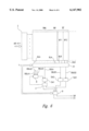
- FIG. 1 is a schematic block diagram of a memory device according to the present invention.
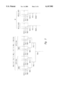
- FIG. 2 is a more detailed view of a memory block of the device shown in FIG. 1, in a first embodiment of the invention.
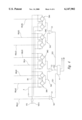
- FIG. 3 is a circuit diagram of a column selection arrangement for the memory block of FIG. 2.
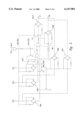
- FIG. 4 is a circuit diagram of a sensing arrangement for the memory block of FIG. 2.
- FIG. 5 is a circuit diagram of an encoding circuit incorporated in the sensing arrangement shown in FIG. 4.
- FIG. 6 is a detailed view of a memory block of the device shown in FIG. 1, in a second embodiment of the present invention.
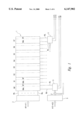
- FIG. 1 shows a schematic block diagram of a memory device according to the present invention.
- the memory device comprises a matrix of memory cells 1.
- the memory matrix 1 is a bidimensional array of memory cells (the latter are not shown, since they are conventional), that are arranged at the intersection of rows (word lines) WL and columns (bit lines) BL.
- the memory matrix includes eight memory blocks B0-B7. Each memory block B0-B7 is associated to two respective data output lines (O0,O1), (O2,O3) . . . (O14,O15) of the memory device.
- a row address decoding circuit 2 receives a subset A0-A11 (row address signals) of a set A0-A21 of address signals.
- the row address decoding circuit 2 decodes the digital code carried by the row address signals A0-A11 and consequently activates one out of 4096 word lines WL.
- the detailed structure of the row address decoding circuit 2 will not be described, being considered well known to the skilled technicians.
- the memory device also conventionally comprises a column address decoding circuit 5 receiving a subset A12-A21 (column address signals) of the set of address signals A0-A21.
- the column address decoding circuit 5 decodes the digital code carried by the column address signals A12-A21, and generates column selection signals Y.
- the detailed structure of the column address decoding circuit 5 will not be described in detail, being considered well known to those skilled in the art.
- Each column selection and sensing circuitry 3 receives the column selection signals Y and accordingly selects a specific column or (as explained later) columns BL among those of the respective memory block B0-B7.
- Block 3 also performs a sensing of the addressed memory cells, i.e., those located at the intersection of the selected row and the selected columns, and controls the logic state of the two respective data output lines (O0,O1) . . . (O14,O15).
- each memory block B0-B7 comprises two memory sub-blocks BML and BF, each including a respective number of memory cells.
- Memory sub-block BML comprises multiple-level non-volatile memory cells, e.g., ROM cells or electrically programmable memory cells such as EPROM cells, fabricated by means of any one of the reliable, conventional processes already known and industrially used for the production of multiple-level non-volatile memories.
- Memory sub-block BF comprises conventional, bilevel electrically erasable and programmable Flash memory cells, fabricated by means of any one of the reliable, conventional processes already known and industrially used for the production of Flash EEPROM memories.
- Memory sub-block BML is not electrically erasable, and has a significantly higher storage capacity than memory sub-block BF, including electrically erasable cells.
- Memory sub-block BML includes for example 1008 columns BLA of multiple-level memory cells, e.g., four-level memory cells.
- Memory sub-block BF includes for example two groups BF1, BF2 each of sixteen columns BLB of conventional, bilevel Flash EEPROM cells.
- Columns BLA and BLB are fed to a column selection circuit 31, the structure of which will be described in detail later in connection with FIG. 3.
- the column selection circuit 31 receives the column selection signals Y.
- Column selection circuit 31 selects one out of the 1008 columns BLA (the selected column of sub-block BML being connected to a first output line SBLA of circuit 31), or one column out of the sixteen columns BLB of each group BF1, BF2 of the Flash sub-block BF (the two selected columns of sub-block BF being connected to two further output lines SBLB1, SBLB2 of circuit 31).
- the output line SBLA of circuit 31 is supplied in parallel to three sense amplifiers SA1, SA2, SA3.
- the other two output lines SBLB1 (selected bit line of group BF1) and SBLB2 (selected bit line of group BF2) are respectively supplied to sense amplifiers SA2 and SA3.
- the outputs SO1, SO2, SO3 of sense amplifiers SA1, SA2, SA3 are supplied to an encoder circuit 4 controlling the logic state of the respective two output lines O0, O1.
- FIG. 3 shows in detail the structure of the column selection circuit 31 shown in FIG. 2.
- column selection scheme provides for three levels of selection. Signals YN0-YN15, YM0-YM15 and YP0-YP3, all belonging to the column selection signals Y, respectively perform a first, a second and a third level of selection.
- the multiple-level cell block BLM comprises in this example 1008 columns BLA. These columns are grouped in packets of sixteen columns each; selection of one column BLA inside each of said packets is made by means of signals YN0-YN15. Three groups of sixteen column packets and one group of fifteen column packets are provided, for a total of 1008 columns BLA. Signals YM0-YM15 allow to select one column packet among the sixteen packets of each one of the first three groups; signals YM0-YM14 allow to select one column packet among the fifteen packets of the last group. Signals YP0-YP3 allow to select one among the groups of column packets.
- signals YN0-YN15 in combination with signals YM15 and YP3, allow to select one out of the sixteen columns BLB of each group of sixteen columns BF1, BF2 of the Flash sub-block BF.
- FIG. 4 shows in greater detail the structure of the sense amplifiers SA1, SA2, SA3.
- the first sense amplifier SA1 comprises a comparator C1 which is supplied directly by the selected column SBLA of sub-block BML and, conventionally, by a first reference column RBLA1 of multiple-level reference memory cells provided inside sub-block BML.
- the second sense amplifier SA2 comprises a comparator C2 and two switches SW1, SW2. Switch SW1 allows to supply one input of comparator C2 with either a second reference column RBLA2 of sub-block BML, or a first reference column RBLB1 of reference Flash EEPROM memory cells associated with group BF1 in sub-block BF.
- Switch SW2 allows to supply the other input of comparator C2 with either the selected column SBLA of sub-block BML, or the selected column SBLB1 of group BF1 in sub-block BF.
- the third sense amplifier SA3 comprises a comparator C3 and two switches SW3, SW4.
- Switch SW3 allows to supply one input of comparator C3 with either a third reference column RBLA3 of sub-block BML, or a reference column RBLB2 associated to group BF2 of sub-block BF.
- Switch SW4 allows to supply the other input of comparator C3 with either the selected column SBLA of sub-block BML, or the selected column SBLB2 of group BF2 in sub-block BF.
- Switches SW1, SW2, SW3 and SW4 are each composed of two CMOS pass gates (i.e., an N-channel MOSFET and a P-channel MOSFET connected in parallel to each other, controlled by complementary signals).
- the first pass gate of each one of the switches is controlled by a signal A which is activated when both signals YM15 and YP3 are activated; the second pass gate of each switch is controlled by a signal AN being the logic complement of signal A.
- comparators C2 and C3 are either supplied with column SBLA and reference columns RBLA2, RBLA3 when either one of signals YM15 or YP3 is deactivated, or they are supplied with columns SBLB1, RBLB1 and SBLB2, RBLB2, respectively, when signals YM15 and YP3 are both activated.
- Reference columns RBLA1, RBLA2, RBLA3 are columns of multiple-level reference memory cells programmed at different programming levels, so that the threshold of comparators C1, C2 and C3 is different.
- FIG. 5 there is shown a detailed circuit diagram of the encoder block 4.
- the encoder 4 comprises an encoding circuit 6.
- Outputs SO2 and SO3 of sense amplifiers SA2 and SA3 are supplied to the encoding circuit 6 through respective first switches SW5 and SW6 and, through respective switches SW7 and SW8, are directly supplied to the respective output lines O0 and O1. All the switches comprise a CMOS pass gate.
- Switches SW5 and SW6 are controlled by a signal MULTIEN which is activated (high logic level) when either one or both of signals YP3 and YM15 is deactivated, i.e., when the multiple-level cell block BML is accessed.
- Switches SW7 and SW8 are controlled by a signal MULTIDIS which is activated (high logic level) when both YP3 and YM15 are activated, i.e., when the Flash cell block B1 is accessed.
- Output SO1 of sense amplifier SA1 is supplied to the decoding circuit 6 through a switch SW11.
- the encoding circuit 6 has two outputs O0' and O1'; substantially circuit 6 performs the following logic operation:
- the outputs O0' and O1' of circuit 6 are connected to the output lines O0, O1 through respective switches SW9, SW10, again formed by a CMOS pass gate, controlled by signal MULTIEN.
- the outputs O0', O1' of circuit 6 are connected to the output lines O0, O1 when the multiple-level cells block BML is accessed, while they are disconnected from the output lines O0, O1 when the Flash cell block BF is accessed; in the latter case, outputs SO2 and SO3 are directly supplied to the output lines O0, O1.
- FIG. 6 there is shown as in FIG. 2 a more detailed structure of a memory block, in a second embodiment of the invention.
- a parallel sensing scheme for sensing the multiple-level memory cells was provided.
- a serial sensing scheme is depicted.
- One of such sensing scheme called “serial-dichotomic”, is described in the European Patent Application No. EP-A-0724266, the relevant disclosure of which is herein incorporated by reference. For this reason, only a brief, schematic description is given in the following.
- sensing of the selected multiple-level cells column SLBA is performed by using only one sense amplifier, namely SA1.
- a state machine 7 is supplied with the output of sense amplifier SA1.
- State machine 7 controls a reference column selection circuit 8 which, depending on the result of the sensing performed by sense amplifier SA1, selects which one of the three reference columns RBLA1, RBLA2, RBLA3 is to be supplied to sense amplifier SA1.
- Sense amplifiers SA2 and SA3 are used to sense in parallel the selected Flash memory cells of columns SBLB1 and SBLB2.
- State machine 7 already provides at its outputs a two-bit code carrying the result of the sensing.
- the two-bit code generated by the state machine 7 is supplied, together with the outputs of sense amplifiers SA2 and SA3, to a logic circuit 9, substantially a switch, allowing for transferring to the output lines O0, O1 either the outputs of state machine 7, or the outputs of sense amplifiers SA2, SA3.
Abstract
Description
O0'=SO3
O1'=(SO1 AND NOT(SO3)) AND SO2.
Claims (13)
Applications Claiming Priority (2)
| Application Number | Priority Date | Filing Date | Title |
|---|---|---|---|
| EP98830324A EP0961287B1 (en) | 1998-05-27 | 1998-05-27 | High storage capacity non-volatile memory |
| EP98830324 | 1998-05-27 |
Publications (1)
| Publication Number | Publication Date |
|---|---|
| US6147902A true US6147902A (en) | 2000-11-14 |
Family
ID=8236663
Family Applications (1)
| Application Number | Title | Priority Date | Filing Date |
|---|---|---|---|
| US09/320,315 Expired - Lifetime US6147902A (en) | 1998-05-27 | 1999-05-26 | High storage capacity non-volatile memory |
Country Status (4)
| Country | Link |
|---|---|
| US (1) | US6147902A (en) |
| EP (1) | EP0961287B1 (en) |
| JP (1) | JP2000057788A (en) |
| DE (1) | DE69820032D1 (en) |
Cited By (4)
| Publication number | Priority date | Publication date | Assignee | Title |
|---|---|---|---|---|
| US6574162B2 (en) * | 2000-02-29 | 2003-06-03 | Fujitsu Limited | Semiconductor memory device utilizing access to memory area located outside main memory area |
| US6622196B1 (en) * | 2000-01-25 | 2003-09-16 | Mitsubishi Denki Kabushiki Kaisha | Method of controlling semiconductor memory device having memory areas with different capacities |
| US20090066547A1 (en) * | 2007-09-07 | 2009-03-12 | Vishal Sarin | Analog-to-digital and digital-to-analog conversion window adjustment based on reference cells in a memory device |
| TWI404068B (en) * | 2007-10-30 | 2013-08-01 | Spansion Llc | Non-volatile memory array partitioning architecture |
Families Citing this family (2)
| Publication number | Priority date | Publication date | Assignee | Title |
|---|---|---|---|---|
| EP1193715A1 (en) * | 2000-09-20 | 2002-04-03 | STMicroelectronics S.r.l. | Nonvolatile memory device, having parts with different access time, reliability and capacity |
| JP4259922B2 (en) * | 2002-07-30 | 2009-04-30 | シャープ株式会社 | Semiconductor memory device |
Citations (9)
| Publication number | Priority date | Publication date | Assignee | Title |
|---|---|---|---|---|
| WO1995034074A1 (en) * | 1994-06-02 | 1995-12-14 | Intel Corporation | Dynamic single to multiple bit per cell memory |
| US5541886A (en) * | 1994-12-27 | 1996-07-30 | Intel Corporation | Method and apparatus for storing control information in multi-bit non-volatile memory arrays |
| EP0724266A1 (en) * | 1995-01-27 | 1996-07-31 | STMicroelectronics S.r.l. | Successive approximation method for sensing multiple-level non-volatile memory cells and sensing circuit using such method |
| US5596526A (en) * | 1995-08-15 | 1997-01-21 | Lexar Microsystems, Inc. | Non-volatile memory system of multi-level transistor cells and methods using same |
| EP0766254A2 (en) * | 1995-09-28 | 1997-04-02 | SANYO ELECTRIC Co., Ltd. | Non-volatile multi-state memory device capable with variable storing resolution |
| US5717632A (en) * | 1996-11-27 | 1998-02-10 | Advanced Micro Devices, Inc. | Apparatus and method for multiple-level storage in non-volatile memories |
| US5754469A (en) * | 1996-06-14 | 1998-05-19 | Macronix International Co., Ltd. | Page mode floating gate memory device storing multiple bits per cell |
| US5844841A (en) * | 1996-04-19 | 1998-12-01 | Kabushiki Kaisha Toshiba | Memory system |
| US5905673A (en) * | 1995-10-06 | 1999-05-18 | Agate Semiconductor, Inc. | Integrated circuit for storage and retrieval of multiple digital bits per nonvolatile memory cell |
Family Cites Families (1)
| Publication number | Priority date | Publication date | Assignee | Title |
|---|---|---|---|---|
| JPH0991972A (en) * | 1995-09-28 | 1997-04-04 | Sanyo Electric Co Ltd | Nonvolatile multilevel memory |
-
1998
- 1998-05-27 EP EP98830324A patent/EP0961287B1/en not_active Expired - Lifetime
- 1998-05-27 DE DE69820032T patent/DE69820032D1/en not_active Expired - Lifetime
-
1999
- 1999-05-21 JP JP14091799A patent/JP2000057788A/en active Pending
- 1999-05-26 US US09/320,315 patent/US6147902A/en not_active Expired - Lifetime
Patent Citations (9)
| Publication number | Priority date | Publication date | Assignee | Title |
|---|---|---|---|---|
| WO1995034074A1 (en) * | 1994-06-02 | 1995-12-14 | Intel Corporation | Dynamic single to multiple bit per cell memory |
| US5541886A (en) * | 1994-12-27 | 1996-07-30 | Intel Corporation | Method and apparatus for storing control information in multi-bit non-volatile memory arrays |
| EP0724266A1 (en) * | 1995-01-27 | 1996-07-31 | STMicroelectronics S.r.l. | Successive approximation method for sensing multiple-level non-volatile memory cells and sensing circuit using such method |
| US5596526A (en) * | 1995-08-15 | 1997-01-21 | Lexar Microsystems, Inc. | Non-volatile memory system of multi-level transistor cells and methods using same |
| EP0766254A2 (en) * | 1995-09-28 | 1997-04-02 | SANYO ELECTRIC Co., Ltd. | Non-volatile multi-state memory device capable with variable storing resolution |
| US5905673A (en) * | 1995-10-06 | 1999-05-18 | Agate Semiconductor, Inc. | Integrated circuit for storage and retrieval of multiple digital bits per nonvolatile memory cell |
| US5844841A (en) * | 1996-04-19 | 1998-12-01 | Kabushiki Kaisha Toshiba | Memory system |
| US5754469A (en) * | 1996-06-14 | 1998-05-19 | Macronix International Co., Ltd. | Page mode floating gate memory device storing multiple bits per cell |
| US5717632A (en) * | 1996-11-27 | 1998-02-10 | Advanced Micro Devices, Inc. | Apparatus and method for multiple-level storage in non-volatile memories |
Cited By (6)
| Publication number | Priority date | Publication date | Assignee | Title |
|---|---|---|---|---|
| US6622196B1 (en) * | 2000-01-25 | 2003-09-16 | Mitsubishi Denki Kabushiki Kaisha | Method of controlling semiconductor memory device having memory areas with different capacities |
| US6574162B2 (en) * | 2000-02-29 | 2003-06-03 | Fujitsu Limited | Semiconductor memory device utilizing access to memory area located outside main memory area |
| US20090066547A1 (en) * | 2007-09-07 | 2009-03-12 | Vishal Sarin | Analog-to-digital and digital-to-analog conversion window adjustment based on reference cells in a memory device |
| US7995412B2 (en) * | 2007-09-07 | 2011-08-09 | Micron Technology, Inc. | Analog-to-digital and digital-to-analog conversion window adjustment based on reference cells in a memory device |
| US8787103B2 (en) | 2007-09-07 | 2014-07-22 | Micron Technology, Inc. | Analog-to-digital and digital-to-analog conversion window adjustment based on reference cells in a memory device |
| TWI404068B (en) * | 2007-10-30 | 2013-08-01 | Spansion Llc | Non-volatile memory array partitioning architecture |
Also Published As
| Publication number | Publication date |
|---|---|
| EP0961287B1 (en) | 2003-11-26 |
| JP2000057788A (en) | 2000-02-25 |
| EP0961287A1 (en) | 1999-12-01 |
| DE69820032D1 (en) | 2004-01-08 |
Similar Documents
| Publication | Publication Date | Title |
|---|---|---|
| US5596526A (en) | Non-volatile memory system of multi-level transistor cells and methods using same | |
| US5808944A (en) | Semiconductor memory device having a defect relief arrangement | |
| US6483742B1 (en) | Bit map addressing schemes for flash memory | |
| US7257026B2 (en) | Non-volatile multi-level semiconductor flash memory device and method of driving same | |
| US6532181B2 (en) | Semiconductor memory device having redundant circuitry for replacing defective memory cell | |
| US5574879A (en) | Addressing modes for a dynamic single bit per cell to multiple bit per cell memory | |
| US6870763B2 (en) | Electrically alterable non-volatile memory with n-bits per cell | |
| EP0806773A1 (en) | Electrically erasable and programmable non-volatile memory device with testable redundancy circuits | |
| KR19980021156A (en) | Nonvolatile Semiconductor Memory Device with Single and Multiple Bit Cells | |
| EP0853806A1 (en) | Integrated circuit for storage and retrieval of multiple digital bits per nonvolatile memory cell | |
| US5854764A (en) | Sectorized electrically erasable and programmable non-volatile memory device with redundancy | |
| US6891755B2 (en) | Architecture for a flash-EEPROM simultaneously readable in other sectors while erasing and/or programming one or more sectors | |
| EP0913834A1 (en) | Nonvolatile semiconductor storage device | |
| US6147902A (en) | High storage capacity non-volatile memory | |
| US6950337B2 (en) | Nonvolatile memory device with simultaneous read/write | |
| EP0825611B1 (en) | Multilevel non-volatile memory devices | |
| US5848000A (en) | Flash memory address decoder with novel latch structure | |
| EP1137011B1 (en) | String programmable nonvolatile memory with NOR architecture | |
| US5654922A (en) | Nonvolatile semiconductor flash memory | |
| US6643174B2 (en) | EEPROM cells and array with reduced write disturbance | |
| EP1750281B1 (en) | Nonvolatile memory device with multiple references and corresponding control method | |
| US6532171B2 (en) | Nonvolatile semiconductor memory capable of selectively erasing a plurality of elemental memory units | |
| Tanzawa et al. | A 44 mm/sup 2/4-bank 8-word page read 64 Mb flash memory with flexible block redundancy and fast accurate word-line voltage controller |
Legal Events
| Date | Code | Title | Description |
|---|---|---|---|
| AS | Assignment |
Owner name: STMICROELECTRONICS S.R.L., ITALY Free format text: ASSIGNMENT OF ASSIGNORS INTEREST;ASSIGNOR:ROLANDI, PAOLO;REEL/FRAME:010015/0475 Effective date: 19990504 |
|
| STCF | Information on status: patent grant |
Free format text: PATENTED CASE |
|
| FEPP | Fee payment procedure |
Free format text: PAYOR NUMBER ASSIGNED (ORIGINAL EVENT CODE: ASPN); ENTITY STATUS OF PATENT OWNER: LARGE ENTITY |
|
| FPAY | Fee payment |
Year of fee payment: 4 |
|
| FPAY | Fee payment |
Year of fee payment: 8 |
|
| FPAY | Fee payment |
Year of fee payment: 12 |
|
| AS | Assignment |
Owner name: MICRON TECHNOLOGY, INC., IDAHO Free format text: ASSIGNMENT OF ASSIGNORS INTEREST;ASSIGNOR:STMICROELECTRONICS, S.R.L. (FORMERLY KNOWN AS SGS-THMSON MICROELECTRONICS S.R.L.);REEL/FRAME:031796/0348 Effective date: 20120523 |
|
| AS | Assignment |
Owner name: U.S. BANK NATIONAL ASSOCIATION, AS COLLATERAL AGENT, CALIFORNIA Free format text: SECURITY INTEREST;ASSIGNOR:MICRON TECHNOLOGY, INC.;REEL/FRAME:038669/0001 Effective date: 20160426 Owner name: U.S. BANK NATIONAL ASSOCIATION, AS COLLATERAL AGEN Free format text: SECURITY INTEREST;ASSIGNOR:MICRON TECHNOLOGY, INC.;REEL/FRAME:038669/0001 Effective date: 20160426 |
|
| AS | Assignment |
Owner name: MORGAN STANLEY SENIOR FUNDING, INC., AS COLLATERAL AGENT, MARYLAND Free format text: PATENT SECURITY AGREEMENT;ASSIGNOR:MICRON TECHNOLOGY, INC.;REEL/FRAME:038954/0001 Effective date: 20160426 Owner name: MORGAN STANLEY SENIOR FUNDING, INC., AS COLLATERAL Free format text: PATENT SECURITY AGREEMENT;ASSIGNOR:MICRON TECHNOLOGY, INC.;REEL/FRAME:038954/0001 Effective date: 20160426 |
|
| AS | Assignment |
Owner name: U.S. BANK NATIONAL ASSOCIATION, AS COLLATERAL AGENT, CALIFORNIA Free format text: CORRECTIVE ASSIGNMENT TO CORRECT THE REPLACE ERRONEOUSLY FILED PATENT #7358718 WITH THE CORRECT PATENT #7358178 PREVIOUSLY RECORDED ON REEL 038669 FRAME 0001. ASSIGNOR(S) HEREBY CONFIRMS THE SECURITY INTEREST;ASSIGNOR:MICRON TECHNOLOGY, INC.;REEL/FRAME:043079/0001 Effective date: 20160426 Owner name: U.S. BANK NATIONAL ASSOCIATION, AS COLLATERAL AGEN Free format text: CORRECTIVE ASSIGNMENT TO CORRECT THE REPLACE ERRONEOUSLY FILED PATENT #7358718 WITH THE CORRECT PATENT #7358178 PREVIOUSLY RECORDED ON REEL 038669 FRAME 0001. ASSIGNOR(S) HEREBY CONFIRMS THE SECURITY INTEREST;ASSIGNOR:MICRON TECHNOLOGY, INC.;REEL/FRAME:043079/0001 Effective date: 20160426 |
|
| AS | Assignment |
Owner name: JPMORGAN CHASE BANK, N.A., AS COLLATERAL AGENT, ILLINOIS Free format text: SECURITY INTEREST;ASSIGNORS:MICRON TECHNOLOGY, INC.;MICRON SEMICONDUCTOR PRODUCTS, INC.;REEL/FRAME:047540/0001 Effective date: 20180703 Owner name: JPMORGAN CHASE BANK, N.A., AS COLLATERAL AGENT, IL Free format text: SECURITY INTEREST;ASSIGNORS:MICRON TECHNOLOGY, INC.;MICRON SEMICONDUCTOR PRODUCTS, INC.;REEL/FRAME:047540/0001 Effective date: 20180703 |
|
| AS | Assignment |
Owner name: MICRON TECHNOLOGY, INC., IDAHO Free format text: RELEASE BY SECURED PARTY;ASSIGNOR:U.S. BANK NATIONAL ASSOCIATION, AS COLLATERAL AGENT;REEL/FRAME:047243/0001 Effective date: 20180629 |
|
| AS | Assignment |
Owner name: MICRON TECHNOLOGY, INC., IDAHO Free format text: RELEASE BY SECURED PARTY;ASSIGNOR:MORGAN STANLEY SENIOR FUNDING, INC., AS COLLATERAL AGENT;REEL/FRAME:050937/0001 Effective date: 20190731 |
|
| AS | Assignment |
Owner name: MICRON TECHNOLOGY, INC., IDAHO Free format text: RELEASE BY SECURED PARTY;ASSIGNOR:JPMORGAN CHASE BANK, N.A., AS COLLATERAL AGENT;REEL/FRAME:051028/0001 Effective date: 20190731 Owner name: MICRON SEMICONDUCTOR PRODUCTS, INC., IDAHO Free format text: RELEASE BY SECURED PARTY;ASSIGNOR:JPMORGAN CHASE BANK, N.A., AS COLLATERAL AGENT;REEL/FRAME:051028/0001 Effective date: 20190731 |