US6150536A - Dye doped organic-inorganic hybrid materials - Google Patents
Dye doped organic-inorganic hybrid materials Download PDFInfo
- Publication number
- US6150536A US6150536A US09/350,429 US35042999A US6150536A US 6150536 A US6150536 A US 6150536A US 35042999 A US35042999 A US 35042999A US 6150536 A US6150536 A US 6150536A
- Authority
- US
- United States
- Prior art keywords
- organic
- component
- dye
- inorganic
- perovskite
- Prior art date
- Legal status (The legal status is an assumption and is not a legal conclusion. Google has not performed a legal analysis and makes no representation as to the accuracy of the status listed.)
- Expired - Fee Related
Links
Images


Classifications
-
- C—CHEMISTRY; METALLURGY
- C07—ORGANIC CHEMISTRY
- C07D—HETEROCYCLIC COMPOUNDS
- C07D409/00—Heterocyclic compounds containing two or more hetero rings, at least one ring having sulfur atoms as the only ring hetero atoms
- C07D409/14—Heterocyclic compounds containing two or more hetero rings, at least one ring having sulfur atoms as the only ring hetero atoms containing three or more hetero rings
-
- C—CHEMISTRY; METALLURGY
- C09—DYES; PAINTS; POLISHES; NATURAL RESINS; ADHESIVES; COMPOSITIONS NOT OTHERWISE PROVIDED FOR; APPLICATIONS OF MATERIALS NOT OTHERWISE PROVIDED FOR
- C09K—MATERIALS FOR MISCELLANEOUS APPLICATIONS, NOT PROVIDED FOR ELSEWHERE
- C09K11/00—Luminescent, e.g. electroluminescent, chemiluminescent materials
- C09K11/06—Luminescent, e.g. electroluminescent, chemiluminescent materials containing organic luminescent materials
-
- C—CHEMISTRY; METALLURGY
- C07—ORGANIC CHEMISTRY
- C07D—HETEROCYCLIC COMPOUNDS
- C07D333/00—Heterocyclic compounds containing five-membered rings having one sulfur atom as the only ring hetero atom
- C07D333/02—Heterocyclic compounds containing five-membered rings having one sulfur atom as the only ring hetero atom not condensed with other rings
- C07D333/04—Heterocyclic compounds containing five-membered rings having one sulfur atom as the only ring hetero atom not condensed with other rings not substituted on the ring sulphur atom
- C07D333/06—Heterocyclic compounds containing five-membered rings having one sulfur atom as the only ring hetero atom not condensed with other rings not substituted on the ring sulphur atom with only hydrogen atoms, hydrocarbon or substituted hydrocarbon radicals, directly attached to the ring carbon atoms
- C07D333/14—Radicals substituted by singly bound hetero atoms other than halogen
- C07D333/18—Radicals substituted by singly bound hetero atoms other than halogen by sulfur atoms
-
- Y—GENERAL TAGGING OF NEW TECHNOLOGICAL DEVELOPMENTS; GENERAL TAGGING OF CROSS-SECTIONAL TECHNOLOGIES SPANNING OVER SEVERAL SECTIONS OF THE IPC; TECHNICAL SUBJECTS COVERED BY FORMER USPC CROSS-REFERENCE ART COLLECTIONS [XRACs] AND DIGESTS
- Y10—TECHNICAL SUBJECTS COVERED BY FORMER USPC
- Y10S—TECHNICAL SUBJECTS COVERED BY FORMER USPC CROSS-REFERENCE ART COLLECTIONS [XRACs] AND DIGESTS
- Y10S977/00—Nanotechnology
- Y10S977/70—Nanostructure
- Y10S977/778—Nanostructure within specified host or matrix material, e.g. nanocomposite films
- Y10S977/783—Organic host/matrix, e.g. lipid
-
- Y—GENERAL TAGGING OF NEW TECHNOLOGICAL DEVELOPMENTS; GENERAL TAGGING OF CROSS-SECTIONAL TECHNOLOGIES SPANNING OVER SEVERAL SECTIONS OF THE IPC; TECHNICAL SUBJECTS COVERED BY FORMER USPC CROSS-REFERENCE ART COLLECTIONS [XRACs] AND DIGESTS
- Y10—TECHNICAL SUBJECTS COVERED BY FORMER USPC
- Y10S—TECHNICAL SUBJECTS COVERED BY FORMER USPC CROSS-REFERENCE ART COLLECTIONS [XRACs] AND DIGESTS
- Y10S977/00—Nanotechnology
- Y10S977/70—Nanostructure
- Y10S977/827—Nanostructure formed from hybrid organic/inorganic semiconductor compositions
-
- Y—GENERAL TAGGING OF NEW TECHNOLOGICAL DEVELOPMENTS; GENERAL TAGGING OF CROSS-SECTIONAL TECHNOLOGIES SPANNING OVER SEVERAL SECTIONS OF THE IPC; TECHNICAL SUBJECTS COVERED BY FORMER USPC CROSS-REFERENCE ART COLLECTIONS [XRACs] AND DIGESTS
- Y10—TECHNICAL SUBJECTS COVERED BY FORMER USPC
- Y10S—TECHNICAL SUBJECTS COVERED BY FORMER USPC CROSS-REFERENCE ART COLLECTIONS [XRACs] AND DIGESTS
- Y10S977/00—Nanotechnology
- Y10S977/902—Specified use of nanostructure
- Y10S977/932—Specified use of nanostructure for electronic or optoelectronic application
- Y10S977/949—Radiation emitter using nanostructure
- Y10S977/95—Electromagnetic energy
-
- Y—GENERAL TAGGING OF NEW TECHNOLOGICAL DEVELOPMENTS; GENERAL TAGGING OF CROSS-SECTIONAL TECHNOLOGIES SPANNING OVER SEVERAL SECTIONS OF THE IPC; TECHNICAL SUBJECTS COVERED BY FORMER USPC CROSS-REFERENCE ART COLLECTIONS [XRACs] AND DIGESTS
- Y10—TECHNICAL SUBJECTS COVERED BY FORMER USPC
- Y10T—TECHNICAL SUBJECTS COVERED BY FORMER US CLASSIFICATION
- Y10T428/00—Stock material or miscellaneous articles
- Y10T428/24—Structurally defined web or sheet [e.g., overall dimension, etc.]
- Y10T428/24942—Structurally defined web or sheet [e.g., overall dimension, etc.] including components having same physical characteristic in differing degree
Definitions
- This invention relates to the field of organic-inorganic hybrid materials. More particularly, it relates to luminescent hybrid materials that may be used in electroluminescent devices.
- Organic-inorganic hybrids are a technologically important class of materials, offering the possibility of combining useful properties of both organic and inorganic components within a single molecular composite.
- Optical and electrical properties of organic materials can be tuned relatively easily by modifying their molecular structure. Their ease of processing, plasticity, and low price make organic materials attractive for a number of applications. Lack of robustness, thermal stability, and low electrical mobility, however, inhibit their use in many of the same applications. These latter properties are offered by inorganic materials. By synthesizing organic-inorganic composites, the best of both worlds can potentially be obtained within a single material.
- the layered organic-inorganic perovskites are a subclass of the organic-inorganic hybrids, and have recently attracted substantial interest due to their potential for unique electrical, magnetic and optical properties.
- the basic building component of this family is the inorganic ABX 3 perovskite structure.
- organic-inorganic hybrid perovskite compounds are formed.
- the organic component is an intimate part of the structure since the structure actually depends on the organic component for charge neutrality. Therefore, the compounds exhibit specific stoichiometries.
- the layered (two-dimensional) A 2 BX 4 , ABX 4 and the one-dimensional A 3 BX 5 , and A 2 A'BX 5 perovskites also exist and are considered derivatives of the three-dimensional parent family.
- the dilution of the dye molecule within the organic component will reduce self-quenching interactions occurring between the dye molecules, which in turn will increase the luminescence yield.
- the present invention relates to an organic-inorganic hybrid material including an organic component and an inorganic component.
- the organic component comprises a dye that luminesces in the visible range.
- an optically inert component can replace a portion of the organic dye component, resulting in an organic-inorganic hybrid material that has a higher intensity luminescence than a hybrid material that is fully loaded with the organic dye.
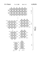
- FIG. 1 illustrates an example of an organic-inorganic hybrid material that is based on a three-dimensional perovskite structure, ABX 3 .
- FIG. 2 illustrates a preferred perovskite structure with the general formula: (RNH 3 ) 2 (CH 3 NH 3 ) n-1 M n X 3n-1 .
- FIG. 4 is a plot of quantum yield vs. dye concentration for a material with the formula AEQT X AETH 1-x PbBr 4 .
- FIG. 5 is the structure of the compound (AEQT)PbBr 4 obtained from a single crystal x-ray structure determination.
- the present invention relates to an organic-inorganic hybrid material containing a dye that luminesces in the visible range.
- the organic-inorganic hybrid material of the present invention combines the advantages of an inorganic crystalline material with those of an organic material.
- the organic component comprises a dye component and an optically inert component that facilitates the self-assembly of the organic-inorganic hybrid material into a crystalline like structure.
- the inorganic component forms an extended one-, two- or three-dimensional network that provides the high carrier mobility characteristic of inorganic crystalline solids.
- the excitons associated with these inorganic networks may be transferred to the organic dye, increasing its emission, especially when the dye is tailored to absorb in the wavelength range of the exciton.
- the luminescence is further enhanced due to a reduction of the self-quenching interactions between the dye molecules.
- a subclass of luminescence is fluorescence (emission arises from allowed transitions, involving singlet excited states and requiring less than 10 -7 to occur).
- an organic-inorganic hybrid material shall mean a material composed of: organic components and inorganic components which are mixed together on a molecular level, and (i) wherein the material is characterized by a substantially fixed ratio of each organic component to each inorganic component; and (ii) wherein both organic and inorganic components manifest forces that enable a self assembly therebetween into a predictable arrangement.
- organic-inorganic hybrid material takes the form of an organic-inorganic perovskite structure.
- Layered perovskites naturally form a quantum well structure in which a two dimensional semiconductor layer of corner sharing metal halide octahedra and an organic layer are alternately stacked.
- FIG. 1 illustrates one example of an organic-inorganic hybrid material 10 that is based on a three-dimensional perovskite structure, ABX 3 .
- the perovskite structure comprises corner-sharing BX 6 octahedra 12.
- Each octahedron 12 is defined by six X anions at the vertices and one B cation in the center (see crystal schematic 18).
- the A cations sit in the large interstices between octahedra 12.
- the organic ammonium or diammonium cation is a mixture of a dye derivative that will luminesce in the visible range and an optically inert material.
- Inorganic perovskite sheets 12 and organic layers 20 are bound by strong, ionic and hydrogen bonding.
- the ionic bonding requires the organic-inorganic compound to have a specific stoichiometry and the organic molecules to sit in well-defined, crystallographic sites.
- the bonding between the organic and inorganic layers causes these hybrid materials to deposit as locally-ordered or crystalline, thin films or to grow as single crystals.
- a preferred perovskite material shown in FIG. 2 has the general formula: (RNH 3 ) 2 (CH 3 NH 3 ) n-1 M n X 3n+1 , wherein R is an organic group; M is a divalent metal, X is a halogen and n is one or more.
- Metal atom 1 is a divalent metal able to adopt an octahedral coordination.
- Organic component 6 is composed of two components: ammonium cation 4 and organic group 3. The ammonium cation 4 hydrogen bonds to the inorganic halogens 2, with organic group 3 extending into the space between the layers and holding the structure together via van der Waals interactions.
- Another preferred perovskite contains a diammonium cation having the general formula (NH 3 --R--NH 3 ) (CH 3 NH 3 ) n-1 M n X 3n+1 , where R, M, X, and n are described above.
- organic component 6 has two ammonium cations 4 that bond to the inorganic halogens 2.
- the organic component is preferably a derivative of a dye that will fluoresce in the visible range.
- preferred dye derivatives are tolan, thioxanthone, coumarin, perylene, oxadiazole, polyenes, oligothiophenes, oligophenylenes, phenylene vinylenes, thiophene vinylenes and mixtures thereof.
- a more preferred organic dye component is 5,5"'-bis(aminoethyl)-2,2':5',2":5",2"'quaterthiophene (AEQT).
- a dye molecule In order for a dye molecule to be suitable for incorporation in the organic-inorganic perovskite structure, several factors must be taken into account during its synthesis: a) One or two unobstructed ammonium units must be attached to the molecule, so that reasonably strong hydrogen bonding can occur between these groups and the perovskite sheet halogens. b) The cross-sectional area of the dye cation must fit within the area defined by the terminal halogens from four adjacent corner-sharing octahedra of the inorganic layers. Dyes with a long and narrow profile are preferable in this respect. The whole gamut of the visual spectrum can be covered by the use of different dyes, an important feature if full color display applications are to be realized.
- a portion of the organic dye component in the organic-inorganic hybrid material is replaced with an optically inert material component.
- An optically inert component is one that does not absorb or fluoresce in the visible range. The incorporation of the optically inert material component may actually increase fluorescence because most dyes self quench in high concentrations.
- the dye concentration should be less than 70 mole %, preferably less than 50 mole %, more preferably less than 20 mole %, still more preferably less than 10 mole % and even more preferably less than 5 mole % based on the total organic component in the organic-inorganic hybrid material.
- any suitable optically inert organic cation material may be used as long as it will bond to the inorganic component to preserve the predicable nature of the hybrid material.
- a preferred optically inert material is 1,6-bis(5'-(2"aminoethyl)-2'-thienyl) hexane (AETH).
- AETH 1,6-bis(5'-(2"aminoethyl)-2'-thienyl) hexane
- Other inert materials can be synthesized using similar design rules as those described above for the dye molecules with, however, the additional constraint that its optical absorption must lie at higher energies than that for the dye, to avoid energy transfer from the dye. Usually, such molecules can be very similar to the dye but modified so they do not emit light. This can be accomplished, for example, by breaking the conjugation (i.e. breaking the sequence of alternating double(or triple) and single bonds).
- a change in the inorganic sheet thickness can vary the conductance of the film.
- the room temperature resistivity decreases with increasing sheet thickness, "n", yielding even a metallic character when n is higher than 3.
- the organic dye component was AEQT and the optically inert material was AETH or bis(5'-(2"-aminoethyl)-2'-thienyl)hexane.
- the film material had the general formula AEQT x AETH 1-x PbBr 4 .
- Measurement of the photoluminescence quantum yield vs. dye concentration is shown in FIG. 4. The data reveals that there is a significant increase in quantum yield as the amount of dye relative to the inert material is decreased. The highest yield measured was when the concentration of the dye was approximately 2 mole %, which was the lowest concentration examined.
- the structure consists of two-dimensional PbBr 4 2- layers 30 of corner-sharing PbBr 6 octahedra, which alternate with layers of diammonium organic cations 31. Strong ionic and hydrogen bonding between the organic and inorganic components give rise to a well-defined structure with a specific stoichiometry.
- Deposition of the material as a thin film can be accomplished by various inexpensive, low temperature methods such as spin-coating, dip-coating or thermal evaporation.
- spin-coating dip-coating
- thermal evaporation a single-source, thermal ablation technique developed by us (U.S. patent application 09/192,130) was employed for the deposition of thin films.
Abstract
Description
Claims (14)
Priority Applications (5)
| Application Number | Priority Date | Filing Date | Title |
|---|---|---|---|
| US09/350,429 US6150536A (en) | 1999-07-08 | 1999-07-08 | Dye doped organic-inorganic hybrid materials |
| KR1020000036220A KR100365107B1 (en) | 1999-07-08 | 2000-06-28 | Dye doped organic-inorganic hybrid materials |
| JP2000205114A JP3606557B2 (en) | 1999-07-08 | 2000-07-06 | Organic-inorganic hybrid material |
| CNB001204106A CN1202203C (en) | 1999-07-08 | 2000-07-07 | Dye adulterated organic-inorganic hybridized material |
| TW089113529A TWI290929B (en) | 1999-07-08 | 2000-07-07 | Dye doped organic-inorganic hybrid materials |
Applications Claiming Priority (1)
| Application Number | Priority Date | Filing Date | Title |
|---|---|---|---|
| US09/350,429 US6150536A (en) | 1999-07-08 | 1999-07-08 | Dye doped organic-inorganic hybrid materials |
Publications (1)
| Publication Number | Publication Date |
|---|---|
| US6150536A true US6150536A (en) | 2000-11-21 |
Family
ID=23376682
Family Applications (1)
| Application Number | Title | Priority Date | Filing Date |
|---|---|---|---|
| US09/350,429 Expired - Fee Related US6150536A (en) | 1999-07-08 | 1999-07-08 | Dye doped organic-inorganic hybrid materials |
Country Status (5)
| Country | Link |
|---|---|
| US (1) | US6150536A (en) |
| JP (1) | JP3606557B2 (en) |
| KR (1) | KR100365107B1 (en) |
| CN (1) | CN1202203C (en) |
| TW (1) | TWI290929B (en) |
Cited By (17)
| Publication number | Priority date | Publication date | Assignee | Title |
|---|---|---|---|---|
| EP1160246A2 (en) * | 2000-05-31 | 2001-12-05 | Consiglio Nazionale Delle Ricerche | Functionalized thiophene oligomers and their use as fluorescent markers |
| US6333418B1 (en) | 1998-07-17 | 2001-12-25 | Astrazeneca Ab | Cyclisation process |
| US20020034838A1 (en) * | 2000-09-18 | 2002-03-21 | Yih Chang | Structure of disturbing plate having bent-down part |
| US6420056B1 (en) * | 1999-07-08 | 2002-07-16 | International Business Machines Corporation | Electroluminescent device with dye-containing organic-inorganic hybrid materials as an emitting layer |
| US6429318B1 (en) * | 2000-02-07 | 2002-08-06 | International Business Machines Corporaiton | Layered organic-inorganic perovskites having metal-deficient inorganic frameworks |
| US20050016462A1 (en) * | 2002-12-12 | 2005-01-27 | Shunpei Yamazaki | Light-emitting device, film-forming method and manufacturing apparatus thereof, and cleaning method of the manufacturing apparatus |
| US20120126216A1 (en) * | 2002-03-08 | 2012-05-24 | International Business Machines Corporation | Low temperature melt-processing of organic-inorganic hybrid |
| WO2015061555A1 (en) * | 2013-10-23 | 2015-04-30 | The Board Of Trustees Of The Leland Stanford Junior University | Two-dimensional perovskite phosphor and method of formation |
| US20160193566A1 (en) * | 2013-09-06 | 2016-07-07 | The Board Of Trusteees Of The Leland Stanford Junior University | Reversible and irreversible chemisorption in nonporous, crystalline hybrid structures |
| US10069025B2 (en) | 2012-09-18 | 2018-09-04 | Oxford University Innovation Limited | Optoelectronic device |
| US10079320B2 (en) | 2012-05-18 | 2018-09-18 | Oxford University Innovation Limited | Optoelectronic device comprising perovskites |
| US10388897B2 (en) | 2012-05-18 | 2019-08-20 | Oxford University Innovation Limited | Optoelectronic device comprising porous scaffold material and perovskites |
| US10403829B2 (en) | 2014-04-18 | 2019-09-03 | Fujifilm Corporation | Photoelectric conversion element, solar cell using the same, and method for manufacturing photoelectric conversion element |
| US10730894B2 (en) * | 2014-08-05 | 2020-08-04 | Korean Research Institute Of Chemical Technology | Method for preparing inorganic/organic hybrid perovskite compound film |
| US11038132B2 (en) | 2012-05-18 | 2021-06-15 | Oxford University Innovation Limited | Optoelectronic devices with organometal perovskites with mixed anions |
| US11078413B2 (en) * | 2016-08-04 | 2021-08-03 | Florida State University Research Foundation, Inc. | Organic-inorganic hybrid perovskites, devices, and methods |
| US11398606B2 (en) * | 2019-01-09 | 2022-07-26 | King Abdullah University Of Science And Technology | 2D hybrid perovskite-based optoelectronic material with smooth external surface |
Families Citing this family (10)
| Publication number | Priority date | Publication date | Assignee | Title |
|---|---|---|---|---|
| JP4729203B2 (en) * | 2001-07-25 | 2011-07-20 | 独立行政法人科学技術振興機構 | Electroluminescent device using phosphorescence of lead halide layered perovskite compound |
| WO2012099177A1 (en) | 2011-01-19 | 2012-07-26 | 住友大阪セメント株式会社 | Organic-inorganic compound and organic-inorganic compound composition as well as ink |
| JP6103183B2 (en) * | 2012-10-10 | 2017-03-29 | ペクセル・テクノロジーズ株式会社 | Electroluminescent device using perovskite compound |
| KR20150135202A (en) * | 2012-12-20 | 2015-12-02 | 이슘 리서치 디벨롭먼트 컴퍼니 오브 더 히브루 유니버시티 오브 예루살렘, 엘티디. | Perovskite schottky type solar cell |
| JP2016132638A (en) * | 2015-01-19 | 2016-07-25 | 三菱化学株式会社 | Organic inorganic perovskite compound, light emitter, semiconductor material, electronic device and solar cell |
| CN105895916B (en) * | 2015-02-13 | 2018-09-07 | 北京大学 | A kind of preparation method and new opplication of organic inorganic hybridization perovskite material |
| CN106910830A (en) * | 2015-12-23 | 2017-06-30 | 昆山工研院新型平板显示技术中心有限公司 | A kind of organic electroluminescence device and preparation method thereof |
| EP3420598B1 (en) * | 2016-02-22 | 2023-12-27 | Alliance for Sustainable Energy, LLC | Methods for producing perovskite halide films |
| KR101877302B1 (en) * | 2016-04-05 | 2018-07-11 | 한국화학연구원 | Inorganic/organic Hybrid Perovskite compound film and Fabrication Method thereof |
| US11476435B2 (en) * | 2017-08-24 | 2022-10-18 | Kyushu University, National University Corporation | Film and organic light-emitting device containing perovskite-type compound and organic light-emitting material |
Citations (2)
| Publication number | Priority date | Publication date | Assignee | Title |
|---|---|---|---|---|
| US5783292A (en) * | 1994-09-29 | 1998-07-21 | Kabushiki Kaisha Toyota Chuo Kenkyusho | Electroluminescent device with organic-inorganic composite thin film |
| US5871579A (en) * | 1997-09-25 | 1999-02-16 | International Business Machines Corporation | Two-step dipping technique for the preparation of organic-inorganic perovskite thin films |
Family Cites Families (1)
| Publication number | Priority date | Publication date | Assignee | Title |
|---|---|---|---|---|
| EP0864182B1 (en) * | 1995-11-28 | 2003-08-13 | International Business Machines Corporation | Organic/inorganic alloys used to improve organic electroluminescent devices |
-
1999
- 1999-07-08 US US09/350,429 patent/US6150536A/en not_active Expired - Fee Related
-
2000
- 2000-06-28 KR KR1020000036220A patent/KR100365107B1/en not_active IP Right Cessation
- 2000-07-06 JP JP2000205114A patent/JP3606557B2/en not_active Expired - Fee Related
- 2000-07-07 CN CNB001204106A patent/CN1202203C/en not_active Expired - Fee Related
- 2000-07-07 TW TW089113529A patent/TWI290929B/en not_active IP Right Cessation
Patent Citations (2)
| Publication number | Priority date | Publication date | Assignee | Title |
|---|---|---|---|---|
| US5783292A (en) * | 1994-09-29 | 1998-07-21 | Kabushiki Kaisha Toyota Chuo Kenkyusho | Electroluminescent device with organic-inorganic composite thin film |
| US5871579A (en) * | 1997-09-25 | 1999-02-16 | International Business Machines Corporation | Two-step dipping technique for the preparation of organic-inorganic perovskite thin films |
Non-Patent Citations (8)
| Title |
|---|
| "Enhanced Phosphorescence from Napthalene-Chromophore Incorporated into Lead Bromide-based layered Perovskite . . . " Era et al., Chem Phys Lett. 296 (1998) 417-420. |
| "PbBr-Based Layered Perovskite Containing Chromophore-Linked Ammonium Molecule as an Organic Layer" Era et al. Chem Lett. (1997) pp. 1235-1236. |
| "Synthesis, Structure and Properties of Organic-Inorganic Perovskites and Related Materials" D. Mitzi, Progress in Inorganic Chemistry, V48, edited by K Karlin, pp. 1.2,89-95 (1999). |
| Appl. Phys. Lett. 65 (6), Aug. 8, 1994, pp. 676 677, M. Era et al., Organic Inorganic Heterostructure Electroluminescent Device Using a Layered Perovskite Semiconductor (C 6 H 5 C 2 H 4 NH 3 ) 2 Pbl4 2 . * |
| Appl. Phys. Lett. 65 (6), Aug. 8, 1994, pp. 676-677, M. Era et al., "Organic-Inorganic Heterostructure Electroluminescent Device Using a Layered Perovskite Semiconductor (C6 H5 C2 H4 NH3)2 Pbl42 ". |
| Enhanced Phosphorescence from Napthalene Chromophore Incorporated into Lead Bromide based layered Perovskite . . . Era et al., Chem Phys Lett. 296 (1998) 417 420. * |
| PbBr Based Layered Perovskite Containing Chromophore Linked Ammonium Molecule as an Organic Layer Era et al. Chem Lett. (1997) pp. 1235 1236. * |
| Synthesis, Structure and Properties of Organic Inorganic Perovskites and Related Materials D. Mitzi, Progress in Inorganic Chemistry, V48, edited by K Karlin, pp. 1.2,89 95 (1999). * |
Cited By (35)
| Publication number | Priority date | Publication date | Assignee | Title |
|---|---|---|---|---|
| US6333418B1 (en) | 1998-07-17 | 2001-12-25 | Astrazeneca Ab | Cyclisation process |
| US6420056B1 (en) * | 1999-07-08 | 2002-07-16 | International Business Machines Corporation | Electroluminescent device with dye-containing organic-inorganic hybrid materials as an emitting layer |
| US6730416B1 (en) * | 1999-07-08 | 2004-05-04 | International Business Machines Corporation | Ionic salt dyes as amorphous, thermally stable emitting and charge transport layers in organic light emitting diodes |
| US6429318B1 (en) * | 2000-02-07 | 2002-08-06 | International Business Machines Corporaiton | Layered organic-inorganic perovskites having metal-deficient inorganic frameworks |
| US6841669B2 (en) | 2000-05-31 | 2005-01-11 | Consiglio Nazionale Delle Ricerche | Functionalized thiophene oligomers and their use as fluorescent markers |
| EP1160246A3 (en) * | 2000-05-31 | 2002-01-30 | Consiglio Nazionale Delle Ricerche | Functionalized thiophene oligomers and their use as fluorescent markers |
| EP1160246A2 (en) * | 2000-05-31 | 2001-12-05 | Consiglio Nazionale Delle Ricerche | Functionalized thiophene oligomers and their use as fluorescent markers |
| US20020034838A1 (en) * | 2000-09-18 | 2002-03-21 | Yih Chang | Structure of disturbing plate having bent-down part |
| US7098097B2 (en) * | 2000-09-18 | 2006-08-29 | Ritdisplay Corporation | Mass-production packaging means and mass-production packaging method |
| US20120126216A1 (en) * | 2002-03-08 | 2012-05-24 | International Business Machines Corporation | Low temperature melt-processing of organic-inorganic hybrid |
| US8574953B2 (en) * | 2002-03-08 | 2013-11-05 | International Business Machines Corporation | Low temperature melt-processing of organic-inorganic hybrid |
| US20050016462A1 (en) * | 2002-12-12 | 2005-01-27 | Shunpei Yamazaki | Light-emitting device, film-forming method and manufacturing apparatus thereof, and cleaning method of the manufacturing apparatus |
| US7583020B2 (en) | 2002-12-12 | 2009-09-01 | Semiconductor Energy Laboratory Co., Ltd. | Light-emitting device, film-forming method and manufacturing apparatus thereof, and cleaning method of the manufacturing apparatus |
| US20090293808A1 (en) * | 2002-12-12 | 2009-12-03 | Semiconductor Energy Laboratory Co., Ltd. | Light-Emitting Device, Film-Forming Method and Manufacturing Apparatus Thereof, and Cleaning Method of the Manufacturing Apparatus |
| US8709540B2 (en) | 2002-12-12 | 2014-04-29 | Semiconductor Energy Laboratory Co., Ltd. | Light-emitting device, film-forming method and manufacturing apparatus thereof, and cleaning method of the manufacturing apparatus |
| US11038132B2 (en) | 2012-05-18 | 2021-06-15 | Oxford University Innovation Limited | Optoelectronic devices with organometal perovskites with mixed anions |
| US11258024B2 (en) | 2012-05-18 | 2022-02-22 | Oxford University Innovation Limited | Optoelectronic devices with organometal perovskites with mixed anions |
| US10079320B2 (en) | 2012-05-18 | 2018-09-18 | Oxford University Innovation Limited | Optoelectronic device comprising perovskites |
| US11908962B2 (en) | 2012-05-18 | 2024-02-20 | Oxford University Innovation Limited | Optoelectronic device comprising perovskites |
| US10388897B2 (en) | 2012-05-18 | 2019-08-20 | Oxford University Innovation Limited | Optoelectronic device comprising porous scaffold material and perovskites |
| US11302833B2 (en) | 2012-05-18 | 2022-04-12 | Oxford University Innovation Limited | Optoelectronic device comprising perovskites |
| US11276734B2 (en) | 2012-05-18 | 2022-03-15 | Oxford University Innovation Limited | Optoelectronic device comprising porous scaffold material and perovskites |
| US10069025B2 (en) | 2012-09-18 | 2018-09-04 | Oxford University Innovation Limited | Optoelectronic device |
| US11527663B2 (en) | 2012-09-18 | 2022-12-13 | Oxford University Innovation Limited | Optoelectronic device |
| US11469338B2 (en) | 2012-09-18 | 2022-10-11 | Oxford University Innovation Limited | Optoelectronic device |
| US10272384B2 (en) * | 2013-09-06 | 2019-04-30 | The Board Of Trustees Of The Leland Stanford Junior University | Reversible and irreversible chemisorption in nonporous, crystalline hybrid structures |
| US20160193566A1 (en) * | 2013-09-06 | 2016-07-07 | The Board Of Trusteees Of The Leland Stanford Junior University | Reversible and irreversible chemisorption in nonporous, crystalline hybrid structures |
| WO2015061555A1 (en) * | 2013-10-23 | 2015-04-30 | The Board Of Trustees Of The Leland Stanford Junior University | Two-dimensional perovskite phosphor and method of formation |
| US11306244B2 (en) | 2013-10-23 | 2022-04-19 | The Board Of Trustees Of The Leland Stanford Junior University | Two-dimensional perovskite phosphor and method of formation |
| US10087366B2 (en) * | 2013-10-23 | 2018-10-02 | The Board Of Trustees Of The Leland Stanford Junior University | Two-dimensional perovskite phosphor and method of formation |
| US10403829B2 (en) | 2014-04-18 | 2019-09-03 | Fujifilm Corporation | Photoelectric conversion element, solar cell using the same, and method for manufacturing photoelectric conversion element |
| US10730894B2 (en) * | 2014-08-05 | 2020-08-04 | Korean Research Institute Of Chemical Technology | Method for preparing inorganic/organic hybrid perovskite compound film |
| US11078413B2 (en) * | 2016-08-04 | 2021-08-03 | Florida State University Research Foundation, Inc. | Organic-inorganic hybrid perovskites, devices, and methods |
| US11926773B2 (en) | 2016-08-04 | 2024-03-12 | Florida State University Research Foundation, Inc. | Organic-inorganic hybrid perovskites, devices, and methods |
| US11398606B2 (en) * | 2019-01-09 | 2022-07-26 | King Abdullah University Of Science And Technology | 2D hybrid perovskite-based optoelectronic material with smooth external surface |
Also Published As
| Publication number | Publication date |
|---|---|
| KR20010049655A (en) | 2001-06-15 |
| JP2001055568A (en) | 2001-02-27 |
| KR100365107B1 (en) | 2002-12-16 |
| TWI290929B (en) | 2007-12-11 |
| CN1202203C (en) | 2005-05-18 |
| JP3606557B2 (en) | 2005-01-05 |
| CN1280167A (en) | 2001-01-17 |
Similar Documents
| Publication | Publication Date | Title |
|---|---|---|
| US6150536A (en) | Dye doped organic-inorganic hybrid materials | |
| US6420056B1 (en) | Electroluminescent device with dye-containing organic-inorganic hybrid materials as an emitting layer | |
| EP1175129B1 (en) | Luminescence device | |
| Wang et al. | Recent progress in luminescent liquid crystal materials: design, properties and application for linearly polarised emission | |
| Gierschner et al. | Luminescent distyrylbenzenes: tailoring molecular structure and crystalline morphology | |
| KR100687666B1 (en) | Electroluminescent Material, Electroluminescent Element and Color Conversion Filter | |
| EP1394870B2 (en) | Phosphorescent organic light emitting device | |
| Fu et al. | Photoluminescence behavior of zero-dimensional manganese halide tetrahedra embedded in conjugated organic matrices | |
| WO2011106990A1 (en) | Light emitting tetraphenylene derivatives, its method for preparation and light emitting device using the same derivatives | |
| Kim et al. | Recent advances in structural design of efficient near‐infrared light‐emitting organic small molecules | |
| Brulatti et al. | Tuning the colour and efficiency in OLEDs by using amorphous or polycrystalline emitting layers | |
| TWI301124B (en) | ||
| JP2005129499A (en) | Organic light-emitting element | |
| KR100936307B1 (en) | Iridium Complex with Improved Luminescent Properties and Organic Electroluminescent Device Containing Iridium Complex | |
| Karatsu et al. | Blue electroluminescence of silyl substituted anthracene derivatives | |
| KR101065541B1 (en) | Solution Processable Red Iridium Complex with Picolinic acid or Picolinic acid-N-oxide Derivatives as Ancillary Ligand and Organic Light-Emitting Diodes Containing Iridium Complex | |
| Brust et al. | Organic Light‐Emitting Diodes Based on Silandiol‐Bay‐Bridged Perylene Bisimides | |
| US7521567B2 (en) | Amine compound and uses thereof | |
| Lin et al. | Regulation and application of organic luminescence from low-dimensional organic-inorganic hybrid metal halides | |
| Murata et al. | Dye-doped molecular light-emitting diodes with enhanced performance | |
| KR20200083923A (en) | Perovskite-based blue light emitting device, and method of preparing the same | |
| TW476227B (en) | Optoelectronic devices containing highly transparent non-metallic cathodes | |
| Stanitska et al. | Molecular design, synthesis, properties, and applications of organic triplet emitters exhibiting blue, green, red and white room temperature phosphorescence | |
| Murata et al. | Molecular organic light-emitting diodes based on a guest-host active layer: Approaches for enhancing device performance | |
| KR100604748B1 (en) | Luminescent material and organic electroluminescent device using the same |
Legal Events
| Date | Code | Title | Description |
|---|---|---|---|
| AS | Assignment |
Owner name: INTERNATIONAL BUSINESS MACHINES CORPORATION, NEW Y Free format text: ASSIGNMENT OF ASSIGNORS INTEREST;ASSIGNORS:CHONDROUDIS, KONSTANTINOS;MITZI, DAVID BRIAN;REEL/FRAME:010106/0343 Effective date: 19990702 |
|
| FEPP | Fee payment procedure |
Free format text: PAYOR NUMBER ASSIGNED (ORIGINAL EVENT CODE: ASPN); ENTITY STATUS OF PATENT OWNER: LARGE ENTITY |
|
| FPAY | Fee payment |
Year of fee payment: 4 |
|
| REMI | Maintenance fee reminder mailed | ||
| LAPS | Lapse for failure to pay maintenance fees | ||
| STCH | Information on status: patent discontinuation |
Free format text: PATENT EXPIRED DUE TO NONPAYMENT OF MAINTENANCE FEES UNDER 37 CFR 1.362 |
|
| FP | Lapsed due to failure to pay maintenance fee |
Effective date: 20081121 |