US6150670A - Process for fabricating a uniform gate oxide of a vertical transistor - Google Patents
Process for fabricating a uniform gate oxide of a vertical transistor Download PDFInfo
- Publication number
- US6150670A US6150670A US09/450,546 US45054699A US6150670A US 6150670 A US6150670 A US 6150670A US 45054699 A US45054699 A US 45054699A US 6150670 A US6150670 A US 6150670A
- Authority
- US
- United States
- Prior art keywords
- trench
- side wall
- sacrificial layer
- nitrogen ions
- vertical transistor
- Prior art date
- Legal status (The legal status is an assumption and is not a legal conclusion. Google has not performed a legal analysis and makes no representation as to the accuracy of the status listed.)
- Expired - Fee Related
Links
- 238000000034 method Methods 0.000 title claims abstract description 24
- 239000013078 crystal Substances 0.000 claims abstract description 53
- IJGRMHOSHXDMSA-UHFFFAOYSA-N nitrogen Substances N#N IJGRMHOSHXDMSA-UHFFFAOYSA-N 0.000 claims abstract description 48
- 229910052757 nitrogen Inorganic materials 0.000 claims abstract description 40
- -1 nitrogen ions Chemical class 0.000 claims abstract description 32
- 239000000758 substrate Substances 0.000 claims abstract description 26
- XUIMIQQOPSSXEZ-UHFFFAOYSA-N Silicon Chemical compound [Si] XUIMIQQOPSSXEZ-UHFFFAOYSA-N 0.000 claims description 21
- 229910052710 silicon Inorganic materials 0.000 claims description 21
- 239000010703 silicon Substances 0.000 claims description 21
- 238000005468 ion implantation Methods 0.000 claims description 8
- 238000002513 implantation Methods 0.000 claims description 6
- 229910052581 Si3N4 Inorganic materials 0.000 claims description 3
- 239000007943 implant Substances 0.000 claims description 3
- HQVNEWCFYHHQES-UHFFFAOYSA-N silicon nitride Chemical compound N12[Si]34N5[Si]62N3[Si]51N64 HQVNEWCFYHHQES-UHFFFAOYSA-N 0.000 claims description 3
- 239000003989 dielectric material Substances 0.000 claims description 2
- 238000000151 deposition Methods 0.000 claims 1
- 230000001590 oxidative effect Effects 0.000 claims 1
- 230000015572 biosynthetic process Effects 0.000 abstract description 4
- 230000003647 oxidation Effects 0.000 description 14
- 238000007254 oxidation reaction Methods 0.000 description 14
- 230000007423 decrease Effects 0.000 description 2
- 229910021420 polycrystalline silicon Inorganic materials 0.000 description 2
- 229920005591 polysilicon Polymers 0.000 description 2
- VYPSYNLAJGMNEJ-UHFFFAOYSA-N Silicium dioxide Chemical compound O=[Si]=O VYPSYNLAJGMNEJ-UHFFFAOYSA-N 0.000 description 1
- 239000003990 capacitor Substances 0.000 description 1
- 230000000694 effects Effects 0.000 description 1
- 238000005530 etching Methods 0.000 description 1
- 230000010354 integration Effects 0.000 description 1
- 239000000463 material Substances 0.000 description 1
- 238000012986 modification Methods 0.000 description 1
- 230000004048 modification Effects 0.000 description 1
- 229910052814 silicon oxide Inorganic materials 0.000 description 1
Images
Classifications
-
- H—ELECTRICITY
- H01—ELECTRIC ELEMENTS
- H01L—SEMICONDUCTOR DEVICES NOT COVERED BY CLASS H10
- H01L21/00—Processes or apparatus adapted for the manufacture or treatment of semiconductor or solid state devices or of parts thereof
- H01L21/02—Manufacture or treatment of semiconductor devices or of parts thereof
- H01L21/04—Manufacture or treatment of semiconductor devices or of parts thereof the devices having at least one potential-jump barrier or surface barrier, e.g. PN junction, depletion layer or carrier concentration layer
- H01L21/18—Manufacture or treatment of semiconductor devices or of parts thereof the devices having at least one potential-jump barrier or surface barrier, e.g. PN junction, depletion layer or carrier concentration layer the devices having semiconductor bodies comprising elements of Group IV of the Periodic System or AIIIBV compounds with or without impurities, e.g. doping materials
- H01L21/26—Bombardment with radiation
- H01L21/263—Bombardment with radiation with high-energy radiation
- H01L21/265—Bombardment with radiation with high-energy radiation producing ion implantation
- H01L21/26506—Bombardment with radiation with high-energy radiation producing ion implantation in group IV semiconductors
-
- H—ELECTRICITY
- H01—ELECTRIC ELEMENTS
- H01L—SEMICONDUCTOR DEVICES NOT COVERED BY CLASS H10
- H01L21/00—Processes or apparatus adapted for the manufacture or treatment of semiconductor or solid state devices or of parts thereof
- H01L21/02—Manufacture or treatment of semiconductor devices or of parts thereof
- H01L21/04—Manufacture or treatment of semiconductor devices or of parts thereof the devices having at least one potential-jump barrier or surface barrier, e.g. PN junction, depletion layer or carrier concentration layer
- H01L21/18—Manufacture or treatment of semiconductor devices or of parts thereof the devices having at least one potential-jump barrier or surface barrier, e.g. PN junction, depletion layer or carrier concentration layer the devices having semiconductor bodies comprising elements of Group IV of the Periodic System or AIIIBV compounds with or without impurities, e.g. doping materials
- H01L21/26—Bombardment with radiation
- H01L21/263—Bombardment with radiation with high-energy radiation
- H01L21/265—Bombardment with radiation with high-energy radiation producing ion implantation
- H01L21/26586—Bombardment with radiation with high-energy radiation producing ion implantation characterised by the angle between the ion beam and the crystal planes or the main crystal surface
-
- H—ELECTRICITY
- H01—ELECTRIC ELEMENTS
- H01L—SEMICONDUCTOR DEVICES NOT COVERED BY CLASS H10
- H01L21/00—Processes or apparatus adapted for the manufacture or treatment of semiconductor or solid state devices or of parts thereof
- H01L21/02—Manufacture or treatment of semiconductor devices or of parts thereof
- H01L21/04—Manufacture or treatment of semiconductor devices or of parts thereof the devices having at least one potential-jump barrier or surface barrier, e.g. PN junction, depletion layer or carrier concentration layer
- H01L21/18—Manufacture or treatment of semiconductor devices or of parts thereof the devices having at least one potential-jump barrier or surface barrier, e.g. PN junction, depletion layer or carrier concentration layer the devices having semiconductor bodies comprising elements of Group IV of the Periodic System or AIIIBV compounds with or without impurities, e.g. doping materials
- H01L21/28—Manufacture of electrodes on semiconductor bodies using processes or apparatus not provided for in groups H01L21/20 - H01L21/268
- H01L21/28008—Making conductor-insulator-semiconductor electrodes
- H01L21/28017—Making conductor-insulator-semiconductor electrodes the insulator being formed after the semiconductor body, the semiconductor being silicon
- H01L21/28158—Making the insulator
- H01L21/28167—Making the insulator on single crystalline silicon, e.g. using a liquid, i.e. chemical oxidation
- H01L21/28211—Making the insulator on single crystalline silicon, e.g. using a liquid, i.e. chemical oxidation in a gaseous ambient using an oxygen or a water vapour, e.g. RTO, possibly through a layer
-
- H—ELECTRICITY
- H01—ELECTRIC ELEMENTS
- H01L—SEMICONDUCTOR DEVICES NOT COVERED BY CLASS H10
- H01L21/00—Processes or apparatus adapted for the manufacture or treatment of semiconductor or solid state devices or of parts thereof
- H01L21/02—Manufacture or treatment of semiconductor devices or of parts thereof
- H01L21/04—Manufacture or treatment of semiconductor devices or of parts thereof the devices having at least one potential-jump barrier or surface barrier, e.g. PN junction, depletion layer or carrier concentration layer
- H01L21/18—Manufacture or treatment of semiconductor devices or of parts thereof the devices having at least one potential-jump barrier or surface barrier, e.g. PN junction, depletion layer or carrier concentration layer the devices having semiconductor bodies comprising elements of Group IV of the Periodic System or AIIIBV compounds with or without impurities, e.g. doping materials
- H01L21/28—Manufacture of electrodes on semiconductor bodies using processes or apparatus not provided for in groups H01L21/20 - H01L21/268
- H01L21/28008—Making conductor-insulator-semiconductor electrodes
- H01L21/28017—Making conductor-insulator-semiconductor electrodes the insulator being formed after the semiconductor body, the semiconductor being silicon
- H01L21/28158—Making the insulator
- H01L21/2822—Making the insulator with substrate doping, e.g. N, Ge, C implantation, before formation of the insulator
-
- H—ELECTRICITY
- H01—ELECTRIC ELEMENTS
- H01L—SEMICONDUCTOR DEVICES NOT COVERED BY CLASS H10
- H01L21/00—Processes or apparatus adapted for the manufacture or treatment of semiconductor or solid state devices or of parts thereof
- H01L21/02—Manufacture or treatment of semiconductor devices or of parts thereof
- H01L21/04—Manufacture or treatment of semiconductor devices or of parts thereof the devices having at least one potential-jump barrier or surface barrier, e.g. PN junction, depletion layer or carrier concentration layer
- H01L21/18—Manufacture or treatment of semiconductor devices or of parts thereof the devices having at least one potential-jump barrier or surface barrier, e.g. PN junction, depletion layer or carrier concentration layer the devices having semiconductor bodies comprising elements of Group IV of the Periodic System or AIIIBV compounds with or without impurities, e.g. doping materials
- H01L21/28—Manufacture of electrodes on semiconductor bodies using processes or apparatus not provided for in groups H01L21/20 - H01L21/268
- H01L21/28008—Making conductor-insulator-semiconductor electrodes
- H01L21/28017—Making conductor-insulator-semiconductor electrodes the insulator being formed after the semiconductor body, the semiconductor being silicon
- H01L21/28158—Making the insulator
- H01L21/28238—Making the insulator with sacrificial oxide
-
- H—ELECTRICITY
- H01—ELECTRIC ELEMENTS
- H01L—SEMICONDUCTOR DEVICES NOT COVERED BY CLASS H10
- H01L29/00—Semiconductor devices adapted for rectifying, amplifying, oscillating or switching, or capacitors or resistors with at least one potential-jump barrier or surface barrier, e.g. PN junction depletion layer or carrier concentration layer; Details of semiconductor bodies or of electrodes thereof ; Multistep manufacturing processes therefor
- H01L29/02—Semiconductor bodies ; Multistep manufacturing processes therefor
- H01L29/04—Semiconductor bodies ; Multistep manufacturing processes therefor characterised by their crystalline structure, e.g. polycrystalline, cubic or particular orientation of crystalline planes
- H01L29/045—Semiconductor bodies ; Multistep manufacturing processes therefor characterised by their crystalline structure, e.g. polycrystalline, cubic or particular orientation of crystalline planes by their particular orientation of crystalline planes
-
- H—ELECTRICITY
- H01—ELECTRIC ELEMENTS
- H01L—SEMICONDUCTOR DEVICES NOT COVERED BY CLASS H10
- H01L29/00—Semiconductor devices adapted for rectifying, amplifying, oscillating or switching, or capacitors or resistors with at least one potential-jump barrier or surface barrier, e.g. PN junction depletion layer or carrier concentration layer; Details of semiconductor bodies or of electrodes thereof ; Multistep manufacturing processes therefor
- H01L29/66—Types of semiconductor device ; Multistep manufacturing processes therefor
- H01L29/66007—Multistep manufacturing processes
- H01L29/66075—Multistep manufacturing processes of devices having semiconductor bodies comprising group 14 or group 13/15 materials
- H01L29/66227—Multistep manufacturing processes of devices having semiconductor bodies comprising group 14 or group 13/15 materials the devices being controllable only by the electric current supplied or the electric potential applied, to an electrode which does not carry the current to be rectified, amplified or switched, e.g. three-terminal devices
- H01L29/66409—Unipolar field-effect transistors
- H01L29/66477—Unipolar field-effect transistors with an insulated gate, i.e. MISFET
- H01L29/66666—Vertical transistors
-
- H—ELECTRICITY
- H01—ELECTRIC ELEMENTS
- H01L—SEMICONDUCTOR DEVICES NOT COVERED BY CLASS H10
- H01L29/00—Semiconductor devices adapted for rectifying, amplifying, oscillating or switching, or capacitors or resistors with at least one potential-jump barrier or surface barrier, e.g. PN junction depletion layer or carrier concentration layer; Details of semiconductor bodies or of electrodes thereof ; Multistep manufacturing processes therefor
- H01L29/66—Types of semiconductor device ; Multistep manufacturing processes therefor
- H01L29/68—Types of semiconductor device ; Multistep manufacturing processes therefor controllable by only the electric current supplied, or only the electric potential applied, to an electrode which does not carry the current to be rectified, amplified or switched
- H01L29/76—Unipolar devices, e.g. field effect transistors
- H01L29/772—Field effect transistors
- H01L29/78—Field effect transistors with field effect produced by an insulated gate
- H01L29/7827—Vertical transistors
-
- H—ELECTRICITY
- H10—SEMICONDUCTOR DEVICES; ELECTRIC SOLID-STATE DEVICES NOT OTHERWISE PROVIDED FOR
- H10B—ELECTRONIC MEMORY DEVICES
- H10B12/00—Dynamic random access memory [DRAM] devices
- H10B12/01—Manufacture or treatment
- H10B12/02—Manufacture or treatment for one transistor one-capacitor [1T-1C] memory cells
- H10B12/05—Making the transistor
- H10B12/053—Making the transistor the transistor being at least partially in a trench in the substrate
-
- H—ELECTRICITY
- H01—ELECTRIC ELEMENTS
- H01L—SEMICONDUCTOR DEVICES NOT COVERED BY CLASS H10
- H01L29/00—Semiconductor devices adapted for rectifying, amplifying, oscillating or switching, or capacitors or resistors with at least one potential-jump barrier or surface barrier, e.g. PN junction depletion layer or carrier concentration layer; Details of semiconductor bodies or of electrodes thereof ; Multistep manufacturing processes therefor
- H01L29/40—Electrodes ; Multistep manufacturing processes therefor
- H01L29/41—Electrodes ; Multistep manufacturing processes therefor characterised by their shape, relative sizes or dispositions
- H01L29/423—Electrodes ; Multistep manufacturing processes therefor characterised by their shape, relative sizes or dispositions not carrying the current to be rectified, amplified or switched
- H01L29/42312—Gate electrodes for field effect devices
- H01L29/42316—Gate electrodes for field effect devices for field-effect transistors
- H01L29/4232—Gate electrodes for field effect devices for field-effect transistors with insulated gate
- H01L29/42356—Disposition, e.g. buried gate electrode
- H01L29/4236—Disposition, e.g. buried gate electrode within a trench, e.g. trench gate electrode, groove gate electrode
-
- H—ELECTRICITY
- H01—ELECTRIC ELEMENTS
- H01L—SEMICONDUCTOR DEVICES NOT COVERED BY CLASS H10
- H01L29/00—Semiconductor devices adapted for rectifying, amplifying, oscillating or switching, or capacitors or resistors with at least one potential-jump barrier or surface barrier, e.g. PN junction depletion layer or carrier concentration layer; Details of semiconductor bodies or of electrodes thereof ; Multistep manufacturing processes therefor
- H01L29/66—Types of semiconductor device ; Multistep manufacturing processes therefor
- H01L29/68—Types of semiconductor device ; Multistep manufacturing processes therefor controllable by only the electric current supplied, or only the electric potential applied, to an electrode which does not carry the current to be rectified, amplified or switched
- H01L29/76—Unipolar devices, e.g. field effect transistors
- H01L29/772—Field effect transistors
- H01L29/78—Field effect transistors with field effect produced by an insulated gate
- H01L29/7801—DMOS transistors, i.e. MISFETs with a channel accommodating body or base region adjoining a drain drift region
- H01L29/7802—Vertical DMOS transistors, i.e. VDMOS transistors
- H01L29/7813—Vertical DMOS transistors, i.e. VDMOS transistors with trench gate electrode, e.g. UMOS transistors
-
- H—ELECTRICITY
- H10—SEMICONDUCTOR DEVICES; ELECTRIC SOLID-STATE DEVICES NOT OTHERWISE PROVIDED FOR
- H10B—ELECTRONIC MEMORY DEVICES
- H10B12/00—Dynamic random access memory [DRAM] devices
- H10B12/01—Manufacture or treatment
- H10B12/02—Manufacture or treatment for one transistor one-capacitor [1T-1C] memory cells
- H10B12/03—Making the capacitor or connections thereto
- H10B12/038—Making the capacitor or connections thereto the capacitor being in a trench in the substrate
- H10B12/0383—Making the capacitor or connections thereto the capacitor being in a trench in the substrate wherein the transistor is vertical
-
- Y—GENERAL TAGGING OF NEW TECHNOLOGICAL DEVELOPMENTS; GENERAL TAGGING OF CROSS-SECTIONAL TECHNOLOGIES SPANNING OVER SEVERAL SECTIONS OF THE IPC; TECHNICAL SUBJECTS COVERED BY FORMER USPC CROSS-REFERENCE ART COLLECTIONS [XRACs] AND DIGESTS
- Y10—TECHNICAL SUBJECTS COVERED BY FORMER USPC
- Y10S—TECHNICAL SUBJECTS COVERED BY FORMER USPC CROSS-REFERENCE ART COLLECTIONS [XRACs] AND DIGESTS
- Y10S438/00—Semiconductor device manufacturing: process
- Y10S438/931—Silicon carbide semiconductor
Definitions
- the present invention relates to a vertical transistor in a trench geometry. More particularly, this invention relates to a process for fabricating a gate oxide of a vertical transistor which has a uniform thickness.
- Gate oxides are typically formed by thermal oxidation of a silicon substrate.
- a crystal structure such as silicon, contains planes of atoms. These planes of atoms influence the properties and behavior of the material. For example, the oxidation rate (R) of a silicon substrate depends on the crystal orientation of the silicon substrate.
- the various planes within crystals such as silicon crystals. This has been done, by convention, using three numbers within brackets called Miller indices.
- the Miller indices that define a lattice plane are simply the reciprocals (cleared of fractions and common multipliers) of the intercepts of the plane with the x, y, and z axes of a rectangular or Cartesian coordinate system.
- the ⁇ 100> plane intercepts the x axis at one and has neither a y-axis intercept nor a z-axis intercept (the reciprocal of infinity is zero); the ⁇ 100> plane is parallel to the y-z plane.
- ⁇ 110> plane which intercepts both the x and y axes at one but has no z-axis intercept.
- the ⁇ 110> plane meets both the x-z plane and the y-z plane at a forty-five degree angle. Note, too, that the ⁇ 110> plane intercepts the ⁇ 100> plane at a forty-five degree angle.
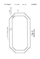
- the thermal oxidation rate (R) of a silicon substrate depends on the crystal orientation of the silicon substrate. More specifically, at the oxidation temperatures of interest, the oxidation rate for a ⁇ 1 10> silicon surface orientation is faster than the rate for a ⁇ 100> silicon surface orientation (R ⁇ 110> >R ⁇ 100> ).
- FIG. 8 illustrates the conventional result: a thicker gate oxide 30 forms on the ⁇ 110> crystal plane than on the ⁇ 100> crystal plane and the oxide thickness is non-uniform.
- the process of Doyle et al. does not address the need to form a gate oxide of a non-planar transistor having a substantially uniform thickness.
- non-planar structures i.e., those structures that do not present a completely uniform, uninterrupted, flat silicon surface
- the silicon substrate consists of multiple crystal planes. Each of the crystal planes has a different oxidation rate.
- the silicon substrate is oxidized to produce the gate oxide, the resulting gate oxide has a varying thickness corresponding to the different crystal planes. Therefore, there remains a need for a process of forming a gate oxide of substantially uniform thickness on non-planar structures.
- the present invention provides a process of forming relatively thin gate oxides of substantially uniform thickness on non-planar structures.
- the invention more specifically provides a process for fabricating a gate oxide of a vertical transistor which has a substantially uniform thickness.
- a trench is formed in a substrate.
- the trench extends from a surface of the substrate and has a trench bottom and a trench side wall.
- the vertical trench side wall comprises ⁇ 100> crystal planes and ⁇ 110> crystal planes.
- a sacrificial layer having a uniform thickness is formed on the trench side wall.
- nitrogen ions are implanted through the sacrificial layer into the ⁇ 110> crystal plane of the trench side wall, with the condition that the nitrogen ions are not implanted into the ⁇ 100> crystal plane of the trench side wall.
- the sacrificial layer is then removed and the trench side wall is oxidized to form the gate oxide.
- the present invention also encompasses the product of the process outlined above. Specifically, the invention provides a vertical transistor having a uniform and relatively thin gate oxide prepared by the foregoing process.
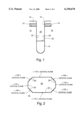
- FIG. 1 shows a cross-sectional view of a trench formed in a substrate
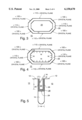
- FIG. 2 shows a top down cross-sectional view of the trench illustrated in FIG. 1, the side wall having four ⁇ 100> crystal planes and four ⁇ 1 10> crystal planes;
- FIG. 3 shows the trench illustrated in FIG. 2 having a sacrificial layer formed on the side wall of the trench
- FIG. 4 shows the trench illustrated in FIG. 3 wherein nitrogen ions are implanted through the sacrificial layer in the direction of the four ⁇ 110> crystal planes;
- FIG. 5 shows a cross sectional view of the structure illustrated in FIG. 4;
- FIG. 6 shows a cross-sectional view of the sacrificial layer and trench side wall illustrated in FIG. 5;
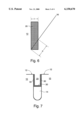
- FIG. 7 shows a cross-sectional view of a gate oxide formed on the trench side wall illustrated in FIG. 1;
- FIG. 8 shows a top down cross-sectional view of a conventional capacitor trench illustrating oxide thickness dependence on crystal plane orientation.
- the process of the invention begins by forming a trench 20 in a substrate 10.
- the substrate 10 is composed of silicon and can also include one or more layers disposed on a surface 12 of the substrate 10, such as a silicon nitride layer 16, a silicon oxide layer 18, or both.
- the resulting structure is illustrated in FIG. 1.
- the trench 20 extends downward from the surface 12 of the substrate 10 and includes a trench side wall 22 and a trench bottom 24.
- a polysilicon layer 14 may be disposed below the bottom 24 of the trench 20.
- a polysilicon layer 14, such as that illustrated in FIG. 1, is conventionally formed at the bottom of vertical structures.
- the trench 20 is formed using techniques that are well known to those of ordinary skill in the art, such as standard photomasking and etching.
- FIG. 2 shows a top down cross-sectional view of the trench 20 illustrated in FIG. 1.
- Non-planar structures such as the trench 20 illustrated in FIG. 2, contain multiple crystal planes.
- the trench side wall 22 illustrated in FIG. 2 has four ⁇ 100> crystal planes and four ⁇ 110> crystal planes.
- the next step of the process of the present invention is applied to the structure illustrated in FIG. 1. That step comprises forming a sacrificial layer 26 on the trench side wall 22. The resulting structure is illustrated in FIG. 3.
- the sacrificial layer 26 is formed on the trench side wall 22 such that the sacrificial layer 26 has a uniform thickness.
- the uniform thickness is shown in FIG. 3 as the thickness "t".
- the sacrificial layer 26 has a thickness of from about 3 nm to about 10 nm.
- the sacrificial layer 26 can be formed using techniques that are well known to those of ordinary skill in the art.
- the sacrificial layer 26 is a deposited dielectric material formed using the high density plasma technique.
- a trench bottom oxide layer (shown in FIG. 5 as trench bottom oxide layer 28) can also be formed on the trench bottom 24.
- nitrogen ions are implanted through the sacrificial layer 26 and into the ⁇ 110> crystal plane of the trench side wall 22. This step is performed while specifically excluding nitrogen ion implantation into the ⁇ 100> crystal plane of the trench side wall 22.
- the nitrogen ion implantation is shown in FIG. 4 along the arrows labeled "NI" for "nitrogen ions.”
- the ⁇ 110> crystal plane of the trench side wall 22 has a greater oxidation rate than the ⁇ 100> crystal plane of the trench side wall 22.
- the thickness t 1 of the gate oxide formed on the ⁇ 110> crystal plane is greater than the thickness t 2 of the gate oxide formed on the ⁇ 100> crystal plane of the trench side wall 22.
- implanting nitrogen ions into the ⁇ 110> crystal plane of the trench side wall 22 preferentially reduces the oxidation rate on the ⁇ 110> crystal plane.
- a gate oxide having a substantially uniform or homogenous thickness can be fabricated.
- the nitrogen ions are implanted through the sacrificial layer 26 and into the trench side wall 22 at an angle ⁇ relative to the top surface 12 of the substrate 10.
- the angle ⁇ of implantation can be calculated by:
- the angle ⁇ is from about 10 degrees to about 60 degrees relative to the top surface 12 of the substrate 10. Even more preferably, the angle ⁇ is between about 30 degrees to about 40 degrees.
- the path "d" of the nitrogen ions through the sacrificial layer 26 to the ⁇ 110> plane can be expressed by the equation:
- E min is the energy necessary to implant the nitrogen ions just through the sacrificial layer 26, but not into the trench side wall 22, and E implantation is the energy of nitrogen ion implantation.
- the nitrogen ions are preferably implanted at a dose from about 2 ⁇ 10 14 /cm 2 to about 1 ⁇ 10 15 /cm 2 .
- the next step of the invention comprises removing the sacrificial layer 26 from the trench side wall 22.
- the sacrificial layer 26 can be removed using techniques that are well known to those of ordinary skill in the art.
- the trench side wall 22 is then oxidized, preferably by thermal oxidation, to produce a gate oxide 30 having a substantially uniform or homogenous thickness.
- the resulting structure is illustrated in FIG. 7.
- the thickness of the gate oxide 30 is relatively thin and may be on the order of about 50 ⁇ when oxidation is performed at about 800° C.
Abstract
Description
cos 45°=d/1 or 0.7×1=d or 1=1.4×d
α=tan.sup.-1 (h/w)
d=t/sin α
E.sub.implantation ≦(1.4)(E.sub.min),
Claims (9)
tan.sup.-1 (h/w)
E.sub.implantation ≦(1.4)(E.sub.min)
Priority Applications (7)
| Application Number | Priority Date | Filing Date | Title |
|---|---|---|---|
| US09/450,546 US6150670A (en) | 1999-11-30 | 1999-11-30 | Process for fabricating a uniform gate oxide of a vertical transistor |
| US09/668,638 US6348388B1 (en) | 1999-11-30 | 2000-09-20 | Process for fabricating a uniform gate oxide of a vertical transistor |
| PCT/US2000/032471 WO2001041201A1 (en) | 1999-11-30 | 2000-11-27 | Process for fabricating a uniform gate oxide of a vertical transistor |
| EP00982265A EP1234325A1 (en) | 1999-11-30 | 2000-11-27 | Process for fabricating a uniform gate oxide of a vertical transistor |
| KR1020027006879A KR20020059817A (en) | 1999-11-30 | 2000-11-27 | Process for fabricating a uniform gate oxide of a vertical transistor |
| JP2001542376A JP2003515952A (en) | 1999-11-30 | 2000-11-27 | Method of forming uniform gate oxide for vertical transistor |
| TW089125321A TW508669B (en) | 1999-11-30 | 2001-03-13 | Process for fabricating a uniform gate oxide of a vertical transistor |
Applications Claiming Priority (1)
| Application Number | Priority Date | Filing Date | Title |
|---|---|---|---|
| US09/450,546 US6150670A (en) | 1999-11-30 | 1999-11-30 | Process for fabricating a uniform gate oxide of a vertical transistor |
Related Child Applications (1)
| Application Number | Title | Priority Date | Filing Date |
|---|---|---|---|
| US09/668,638 Division US6348388B1 (en) | 1999-11-30 | 2000-09-20 | Process for fabricating a uniform gate oxide of a vertical transistor |
Publications (1)
| Publication Number | Publication Date |
|---|---|
| US6150670A true US6150670A (en) | 2000-11-21 |
Family
ID=23788516
Family Applications (2)
| Application Number | Title | Priority Date | Filing Date |
|---|---|---|---|
| US09/450,546 Expired - Fee Related US6150670A (en) | 1999-11-30 | 1999-11-30 | Process for fabricating a uniform gate oxide of a vertical transistor |
| US09/668,638 Expired - Fee Related US6348388B1 (en) | 1999-11-30 | 2000-09-20 | Process for fabricating a uniform gate oxide of a vertical transistor |
Family Applications After (1)
| Application Number | Title | Priority Date | Filing Date |
|---|---|---|---|
| US09/668,638 Expired - Fee Related US6348388B1 (en) | 1999-11-30 | 2000-09-20 | Process for fabricating a uniform gate oxide of a vertical transistor |
Country Status (6)
| Country | Link |
|---|---|
| US (2) | US6150670A (en) |
| EP (1) | EP1234325A1 (en) |
| JP (1) | JP2003515952A (en) |
| KR (1) | KR20020059817A (en) |
| TW (1) | TW508669B (en) |
| WO (1) | WO2001041201A1 (en) |
Cited By (15)
| Publication number | Priority date | Publication date | Assignee | Title |
|---|---|---|---|---|
| WO2001082333A2 (en) * | 2000-04-20 | 2001-11-01 | Infineon Technologies North America Corp. | Homogeneous gate oxide thickness for vertical transistor structures |
| US6348388B1 (en) * | 1999-11-30 | 2002-02-19 | International Business Machines Corporation | Process for fabricating a uniform gate oxide of a vertical transistor |
| US6420239B2 (en) * | 2000-05-31 | 2002-07-16 | Infineon Technologies Ag | Memory cell with trench capacitor and method of fabricating the memory cell |
| US20020197868A1 (en) * | 2001-06-22 | 2002-12-26 | Tetsuo Endoh | Method for evaluating dependence of properties of semiconductor substrate on plane orientation and semiconductor device using the same |
| EP1296369A1 (en) * | 2001-09-20 | 2003-03-26 | Infineon Technologies AG | Method of making gate oxide for trench gate DRAM cells |
| US6544855B1 (en) | 2001-10-19 | 2003-04-08 | Infineon Technologies Ag | Process flow for sacrificial collar with polysilicon void |
| US6551942B2 (en) | 2001-06-15 | 2003-04-22 | International Business Machines Corporation | Methods for etching tungsten stack structures |
| US6566273B2 (en) * | 2001-06-27 | 2003-05-20 | Infineon Technologies Ag | Etch selectivity inversion for etching along crystallographic directions in silicon |
| US6605501B1 (en) | 2002-06-06 | 2003-08-12 | Chartered Semiconductor Manufacturing Ltd. | Method of fabricating CMOS device with dual gate electrode |
| US6610575B1 (en) | 2002-06-04 | 2003-08-26 | Chartered Semiconductor Manufacturing Ltd. | Forming dual gate oxide thickness on vertical transistors by ion implantation |
| US20030235959A1 (en) * | 2002-06-25 | 2003-12-25 | Siliconix Incorporated | Self-aligned differential oxidation in trenches by ion implantation |
| US20060113590A1 (en) * | 2004-11-26 | 2006-06-01 | Samsung Electronics Co., Ltd. | Method of forming a recess structure, recessed channel type transistor and method of manufacturing the recessed channel type transistor |
| WO2008118531A2 (en) * | 2007-01-30 | 2008-10-02 | Aviza Technology, Inc. | Oxide-containing film formed from silicon |
| CN104347472A (en) * | 2013-07-29 | 2015-02-11 | 中芯国际集成电路制造(上海)有限公司 | Manufacturing method of shallow trench isolation |
| US10643852B2 (en) | 2016-09-30 | 2020-05-05 | Semiconductor Components Industries, Llc | Process of forming an electronic device including exposing a substrate to an oxidizing ambient |
Families Citing this family (23)
| Publication number | Priority date | Publication date | Assignee | Title |
|---|---|---|---|---|
| US6740555B1 (en) * | 1999-09-29 | 2004-05-25 | Infineon Technologies Ag | Semiconductor structures and manufacturing methods |
| US6437381B1 (en) * | 2000-04-27 | 2002-08-20 | International Business Machines Corporation | Semiconductor memory device with reduced orientation-dependent oxidation in trench structures |
| US20020172980A1 (en) * | 2000-11-27 | 2002-11-21 | Phan Brigitte Chau | Methods for decreasing non-specific binding of beads in dual bead assays including related optical biodiscs and disc drive systems |
| US20030003464A1 (en) * | 2000-11-27 | 2003-01-02 | Phan Brigitte C. | Dual bead assays including optical biodiscs and methods relating thereto |
| US20040248093A1 (en) * | 2000-11-27 | 2004-12-09 | Coombs James Howard | Magneto-optical bio-discs and systems including related methods |
| JP4865166B2 (en) * | 2001-08-30 | 2012-02-01 | 新電元工業株式会社 | Transistor manufacturing method, diode manufacturing method |
| US6686604B2 (en) * | 2001-09-21 | 2004-02-03 | Agere Systems Inc. | Multiple operating voltage vertical replacement-gate (VRG) transistor |
| US6762094B2 (en) | 2002-09-27 | 2004-07-13 | Hewlett-Packard Development Company, L.P. | Nanometer-scale semiconductor devices and method of making |
| US6727142B1 (en) | 2002-10-29 | 2004-04-27 | International Business Machines Corporation | Orientation independent oxidation of nitrided silicon |
| US6909151B2 (en) | 2003-06-27 | 2005-06-21 | Intel Corporation | Nonplanar device with stress incorporation layer and method of fabrication |
| US20070034909A1 (en) * | 2003-09-22 | 2007-02-15 | James Stasiak | Nanometer-scale semiconductor devices and method of making |
| US7042009B2 (en) | 2004-06-30 | 2006-05-09 | Intel Corporation | High mobility tri-gate devices and methods of fabrication |
| US7348284B2 (en) | 2004-08-10 | 2008-03-25 | Intel Corporation | Non-planar pMOS structure with a strained channel region and an integrated strained CMOS flow |
| US7422946B2 (en) | 2004-09-29 | 2008-09-09 | Intel Corporation | Independently accessed double-gate and tri-gate transistors in same process flow |
| US20060086977A1 (en) | 2004-10-25 | 2006-04-27 | Uday Shah | Nonplanar device with thinned lower body portion and method of fabrication |
| US7518196B2 (en) | 2005-02-23 | 2009-04-14 | Intel Corporation | Field effect transistor with narrow bandgap source and drain regions and method of fabrication |
| JP5017855B2 (en) * | 2005-12-14 | 2012-09-05 | 富士電機株式会社 | Manufacturing method of semiconductor device |
| JP5167593B2 (en) * | 2006-03-23 | 2013-03-21 | 富士電機株式会社 | Semiconductor device |
| US8362566B2 (en) | 2008-06-23 | 2013-01-29 | Intel Corporation | Stress in trigate devices using complimentary gate fill materials |
| JP5395309B2 (en) | 2011-03-23 | 2014-01-22 | パナソニック株式会社 | Semiconductor device and manufacturing method thereof |
| US10522549B2 (en) * | 2018-02-17 | 2019-12-31 | Varian Semiconductor Equipment Associates, Inc. | Uniform gate dielectric for DRAM device |
| JP7295052B2 (en) * | 2020-02-28 | 2023-06-20 | 株式会社東芝 | semiconductor equipment |
| JPWO2021186911A1 (en) * | 2020-03-18 | 2021-09-23 |
Citations (7)
| Publication number | Priority date | Publication date | Assignee | Title |
|---|---|---|---|---|
| US4397075A (en) * | 1980-07-03 | 1983-08-09 | International Business Machines Corporation | FET Memory cell structure and process |
| US4503601A (en) * | 1983-04-18 | 1985-03-12 | Ncr Corporation | Oxide trench structure for polysilicon gates and interconnects |
| US4990462A (en) * | 1989-04-12 | 1991-02-05 | Advanced Micro Devices, Inc. | Method for coplanar integration of semiconductor ic devices |
| US5075253A (en) * | 1989-04-12 | 1991-12-24 | Advanced Micro Devices, Inc. | Method of coplanar integration of semiconductor IC devices |
| US5670805A (en) * | 1995-03-29 | 1997-09-23 | Kabushiki Kaisha Toshiba | Controlled recrystallization of buried strap in a semiconductor memory device |
| US5744826A (en) * | 1996-01-23 | 1998-04-28 | Denso Corporation | Silicon carbide semiconductor device and process for its production |
| US5869858A (en) * | 1995-03-14 | 1999-02-09 | Kabushiki Kaisha Toshiba | Semiconductor device for reducing variations in characteristics of the device |
Family Cites Families (19)
| Publication number | Priority date | Publication date | Assignee | Title |
|---|---|---|---|---|
| EP0283964B1 (en) * | 1987-03-20 | 1994-09-28 | Nec Corporation | Dynamic random access memory device having a plurality of improved one-transistor type memory cells |
| JPH05109984A (en) * | 1991-05-27 | 1993-04-30 | Mitsubishi Electric Corp | Semiconductor device and its manufacture |
| US5330920A (en) * | 1993-06-15 | 1994-07-19 | Digital Equipment Corporation | Method of controlling gate oxide thickness in the fabrication of semiconductor devices |
| US6127242A (en) * | 1994-02-10 | 2000-10-03 | Micron Technology, Inc. | Method for semiconductor device isolation using oxygen and nitrogen ion implantations to reduce lateral encroachment |
| US5698893A (en) * | 1995-01-03 | 1997-12-16 | Motorola, Inc. | Static-random-access memory cell with trench transistor and enhanced stability |
| SG50741A1 (en) * | 1995-07-26 | 1998-07-20 | Chartered Semiconductor Mfg | Method for minimizing the hot carrier effect in m-mosfet devices |
| US5670406A (en) * | 1997-01-30 | 1997-09-23 | Vanguard International Semiconductor Corporation | Method of making a tooth shaped capacitor |
| GB2327810B (en) * | 1997-02-07 | 1999-06-09 | United Microelectronics Corp | Manufacturing integrated circuit devices with different gate oxide thicknesses |
| US5899716A (en) * | 1997-05-19 | 1999-05-04 | Vanguard International Semiconductor Corporation | Oxygen ion implantation procedure to increase the surface area of an STC structure |
| US5920782A (en) * | 1997-07-18 | 1999-07-06 | United Microelectronics Corp. | Method for improving hot carrier degradation |
| US5858846A (en) * | 1997-08-04 | 1999-01-12 | Taiwan Semiconductor Manufacturing Company, Ltd. | Salicide integration method |
| US6002160A (en) * | 1997-12-12 | 1999-12-14 | Advanced Micro Devices, Inc. | Semiconductor isolation process to minimize weak oxide problems |
| DE19807776A1 (en) * | 1998-02-24 | 1999-09-02 | Siemens Ag | Semiconductor device and corresponding manufacturing method |
| US6090653A (en) * | 1998-03-30 | 2000-07-18 | Texas Instruments | Method of manufacturing CMOS transistors |
| US6238998B1 (en) * | 1998-11-20 | 2001-05-29 | International Business Machines Corporation | Shallow trench isolation on a silicon substrate using nitrogen implant into the side wall |
| US6245639B1 (en) * | 1999-02-08 | 2001-06-12 | Taiwan Semiconductor Manufacturing Company | Method to reduce a reverse narrow channel effect for MOSFET devices |
| US6229184B1 (en) * | 1999-02-16 | 2001-05-08 | Advanced Micro Devices, Inc. | Semiconductor device with a modulated gate oxide thickness |
| US6200863B1 (en) * | 1999-03-24 | 2001-03-13 | Advanced Micro Devices, Inc. | Process for fabricating a semiconductor device having assymetric source-drain extension regions |
| US6150670A (en) * | 1999-11-30 | 2000-11-21 | International Business Machines Corporation | Process for fabricating a uniform gate oxide of a vertical transistor |
-
1999
- 1999-11-30 US US09/450,546 patent/US6150670A/en not_active Expired - Fee Related
-
2000
- 2000-09-20 US US09/668,638 patent/US6348388B1/en not_active Expired - Fee Related
- 2000-11-27 WO PCT/US2000/032471 patent/WO2001041201A1/en not_active Application Discontinuation
- 2000-11-27 KR KR1020027006879A patent/KR20020059817A/en active IP Right Grant
- 2000-11-27 EP EP00982265A patent/EP1234325A1/en not_active Withdrawn
- 2000-11-27 JP JP2001542376A patent/JP2003515952A/en active Pending
-
2001
- 2001-03-13 TW TW089125321A patent/TW508669B/en not_active IP Right Cessation
Patent Citations (7)
| Publication number | Priority date | Publication date | Assignee | Title |
|---|---|---|---|---|
| US4397075A (en) * | 1980-07-03 | 1983-08-09 | International Business Machines Corporation | FET Memory cell structure and process |
| US4503601A (en) * | 1983-04-18 | 1985-03-12 | Ncr Corporation | Oxide trench structure for polysilicon gates and interconnects |
| US4990462A (en) * | 1989-04-12 | 1991-02-05 | Advanced Micro Devices, Inc. | Method for coplanar integration of semiconductor ic devices |
| US5075253A (en) * | 1989-04-12 | 1991-12-24 | Advanced Micro Devices, Inc. | Method of coplanar integration of semiconductor IC devices |
| US5869858A (en) * | 1995-03-14 | 1999-02-09 | Kabushiki Kaisha Toshiba | Semiconductor device for reducing variations in characteristics of the device |
| US5670805A (en) * | 1995-03-29 | 1997-09-23 | Kabushiki Kaisha Toshiba | Controlled recrystallization of buried strap in a semiconductor memory device |
| US5744826A (en) * | 1996-01-23 | 1998-04-28 | Denso Corporation | Silicon carbide semiconductor device and process for its production |
Non-Patent Citations (4)
| Title |
|---|
| Doyle et al., "Simultaneous Growth of Different Thickness Gate Oxides in Silicon CMOS Processing," IEEE Electronic Device Letters, vol. 16, No. 7, pp. 301-302 (Jul. 1995). |
| Doyle et al., Simultaneous Growth of Different Thickness Gate Oxides in Silicon CMOS Processing, IEEE Electronic Device Letters, vol. 16, No. 7, pp. 301 302 (Jul. 1995). * |
| Irene et al., "Silicon Oxidation Studies: Silicon Orientation Effects on Thermal Oxidation," J. Electrochem. Soc., vol. 133, No. 6, pp. 1253-1256 (Jun. 1986). |
| Irene et al., Silicon Oxidation Studies: Silicon Orientation Effects on Thermal Oxidation, J. Electrochem. Soc., vol. 133, No. 6, pp. 1253 1256 (Jun. 1986). * |
Cited By (24)
| Publication number | Priority date | Publication date | Assignee | Title |
|---|---|---|---|---|
| US6348388B1 (en) * | 1999-11-30 | 2002-02-19 | International Business Machines Corporation | Process for fabricating a uniform gate oxide of a vertical transistor |
| WO2001082333A3 (en) * | 2000-04-20 | 2002-01-24 | Infineon Technologies Corp | Homogeneous gate oxide thickness for vertical transistor structures |
| WO2001082333A2 (en) * | 2000-04-20 | 2001-11-01 | Infineon Technologies North America Corp. | Homogeneous gate oxide thickness for vertical transistor structures |
| US6420239B2 (en) * | 2000-05-31 | 2002-07-16 | Infineon Technologies Ag | Memory cell with trench capacitor and method of fabricating the memory cell |
| US6551942B2 (en) | 2001-06-15 | 2003-04-22 | International Business Machines Corporation | Methods for etching tungsten stack structures |
| US20020197868A1 (en) * | 2001-06-22 | 2002-12-26 | Tetsuo Endoh | Method for evaluating dependence of properties of semiconductor substrate on plane orientation and semiconductor device using the same |
| KR100497051B1 (en) * | 2001-06-22 | 2005-06-23 | 샤프 가부시키가이샤 | Method for evaluating dependence of properties of semiconductor substrate on plane orientation and semiconductor device using the same |
| US7141506B2 (en) * | 2001-06-22 | 2006-11-28 | Sharp Kabushiki Kaisha | Method for evaluating dependence of properties of semiconductor substrate on plane orientation and semiconductor device using the same |
| DE10226883B4 (en) * | 2001-06-27 | 2010-07-15 | Qimonda Ag | Etching selectivity inversion for etching along crystal directions in silicon |
| US6566273B2 (en) * | 2001-06-27 | 2003-05-20 | Infineon Technologies Ag | Etch selectivity inversion for etching along crystallographic directions in silicon |
| EP1296369A1 (en) * | 2001-09-20 | 2003-03-26 | Infineon Technologies AG | Method of making gate oxide for trench gate DRAM cells |
| US6544855B1 (en) | 2001-10-19 | 2003-04-08 | Infineon Technologies Ag | Process flow for sacrificial collar with polysilicon void |
| US6610575B1 (en) | 2002-06-04 | 2003-08-26 | Chartered Semiconductor Manufacturing Ltd. | Forming dual gate oxide thickness on vertical transistors by ion implantation |
| US6605501B1 (en) | 2002-06-06 | 2003-08-12 | Chartered Semiconductor Manufacturing Ltd. | Method of fabricating CMOS device with dual gate electrode |
| EP1376674A2 (en) * | 2002-06-25 | 2004-01-02 | Siliconix Incorporated | Method of fabricating a trench MOSFET |
| US7012005B2 (en) | 2002-06-25 | 2006-03-14 | Siliconix Incorporated | Self-aligned differential oxidation in trenches by ion implantation |
| EP1376674A3 (en) * | 2002-06-25 | 2005-02-02 | Siliconix Incorporated | Method of fabricating a trench MOSFET |
| US20030235959A1 (en) * | 2002-06-25 | 2003-12-25 | Siliconix Incorporated | Self-aligned differential oxidation in trenches by ion implantation |
| US20060113590A1 (en) * | 2004-11-26 | 2006-06-01 | Samsung Electronics Co., Ltd. | Method of forming a recess structure, recessed channel type transistor and method of manufacturing the recessed channel type transistor |
| WO2008118531A2 (en) * | 2007-01-30 | 2008-10-02 | Aviza Technology, Inc. | Oxide-containing film formed from silicon |
| WO2008118531A3 (en) * | 2007-01-30 | 2009-05-07 | Aviza Tech Inc | Oxide-containing film formed from silicon |
| US20100117203A1 (en) * | 2007-01-30 | 2010-05-13 | Aviza Technology, Inc. | Oxide-containing film formed from silicon |
| CN104347472A (en) * | 2013-07-29 | 2015-02-11 | 中芯国际集成电路制造(上海)有限公司 | Manufacturing method of shallow trench isolation |
| US10643852B2 (en) | 2016-09-30 | 2020-05-05 | Semiconductor Components Industries, Llc | Process of forming an electronic device including exposing a substrate to an oxidizing ambient |
Also Published As
| Publication number | Publication date |
|---|---|
| JP2003515952A (en) | 2003-05-07 |
| US6348388B1 (en) | 2002-02-19 |
| WO2001041201A9 (en) | 2002-05-30 |
| TW508669B (en) | 2002-11-01 |
| KR20020059817A (en) | 2002-07-13 |
| WO2001041201A1 (en) | 2001-06-07 |
| EP1234325A1 (en) | 2002-08-28 |
Similar Documents
| Publication | Publication Date | Title |
|---|---|---|
| US6150670A (en) | Process for fabricating a uniform gate oxide of a vertical transistor | |
| US6998667B2 (en) | Scalable gate and storage dielectric | |
| US7317226B2 (en) | Patterned SOI by oxygen implantation and annealing | |
| EP1358669B1 (en) | Dynamic memory based on single electron storage | |
| EP1150349A2 (en) | Process for reduction of orientation-dependent oxidation in trench structures and semiconductor memory device produced thereby | |
| US6846727B2 (en) | Patterned SOI by oxygen implantation and annealing | |
| US10090287B1 (en) | Deep high capacity capacitor for bulk substrates | |
| JP2937395B2 (en) | Semiconductor element | |
| JP3262059B2 (en) | Method for manufacturing semiconductor device | |
| US8013396B2 (en) | Semiconductor component and semiconductor device | |
| US6821864B2 (en) | Method to achieve increased trench depth, independent of CD as defined by lithography | |
| US6653185B2 (en) | Method of providing trench walls by using two-step etching processes | |
| KR100707169B1 (en) | Memory Device and Manufacturing Method thereof | |
| TWI324827B (en) | Transistor element having an anisotropic high-k gate dielectric | |
| JPS60198841A (en) | Element isolation of semiconductor device | |
| US20230122234A1 (en) | Stacked vertical transport field effect transistor with anchors | |
| US6037198A (en) | Method of fabricating SOI wafer | |
| US7566919B2 (en) | Method to reduce seedlayer topography in BICMOS process | |
| JP3149820B2 (en) | Method for manufacturing semiconductor device | |
| CN115274452A (en) | Preparation method of ferroelectric 3D stacked gate-all-around transistor | |
| JPH0294466A (en) | Double-capacitor and its manufacture | |
| US20080073699A1 (en) | Semiconductor device and method for manufacturing semiconductor device | |
| TW200901384A (en) | Method for manufacturing semiconductor device with out-diffusion suppression |
Legal Events
| Date | Code | Title | Description |
|---|---|---|---|
| AS | Assignment |
Owner name: INTERNATIONAL BUSINESS MACHINES CORPORATION, NEW Y Free format text: ASSIGNMENT OF ASSIGNORS INTEREST;ASSIGNORS:FALTERMEIER, JOHNATHAN E.;HEGDE, SURYANARAYAN G.;JAMMY, RAJARAO;REEL/FRAME:010423/0079;SIGNING DATES FROM 19991123 TO 19991129 Owner name: INFINEON TECHNOLOGIES NORTH AMERICA CORP., CALIFOR Free format text: ASSIGNMENT OF ASSIGNORS INTEREST;ASSIGNORS:GRUENING, ULRIKE;LEE, BRIAN S.;TEWS, HELMUT H.;REEL/FRAME:010423/0164;SIGNING DATES FROM 19991123 TO 19991129 |
|
| AS | Assignment |
Owner name: INFINEON TECHNOLOGIES AG, GERMANY Free format text: ASSIGNMENT OF ASSIGNORS INTEREST;ASSIGNOR:INFINEON TECHNOLOGIES NORTH AMERICA CORP.;REEL/FRAME:012670/0047 Effective date: 20020211 |
|
| FEPP | Fee payment procedure |
Free format text: PAYOR NUMBER ASSIGNED (ORIGINAL EVENT CODE: ASPN); ENTITY STATUS OF PATENT OWNER: LARGE ENTITY |
|
| FPAY | Fee payment |
Year of fee payment: 4 |
|
| FEPP | Fee payment procedure |
Free format text: PAYER NUMBER DE-ASSIGNED (ORIGINAL EVENT CODE: RMPN); ENTITY STATUS OF PATENT OWNER: LARGE ENTITY Free format text: PAYOR NUMBER ASSIGNED (ORIGINAL EVENT CODE: ASPN); ENTITY STATUS OF PATENT OWNER: LARGE ENTITY |
|
| REMI | Maintenance fee reminder mailed | ||
| LAPS | Lapse for failure to pay maintenance fees | ||
| STCH | Information on status: patent discontinuation |
Free format text: PATENT EXPIRED DUE TO NONPAYMENT OF MAINTENANCE FEES UNDER 37 CFR 1.362 |
|
| FP | Lapsed due to failure to pay maintenance fee |
Effective date: 20081121 |
|
| AS | Assignment |
Owner name: QIMONDA AG, GERMANY Free format text: ASSIGNMENT OF ASSIGNORS INTEREST;ASSIGNOR:INFINEON TECHNOLOGIES AG;REEL/FRAME:023853/0401 Effective date: 20060425 |