US6150847A - Device and method for generating a variable duty cycle clock - Google Patents
Device and method for generating a variable duty cycle clock Download PDFInfo
- Publication number
- US6150847A US6150847A US09/358,013 US35801399A US6150847A US 6150847 A US6150847 A US 6150847A US 35801399 A US35801399 A US 35801399A US 6150847 A US6150847 A US 6150847A
- Authority
- US
- United States
- Prior art keywords
- clock
- delay
- clocks
- duty cycle
- variable duty
- Prior art date
- Legal status (The legal status is an assumption and is not a legal conclusion. Google has not performed a legal analysis and makes no representation as to the accuracy of the status listed.)
- Expired - Lifetime
Links
Images


Classifications
-
- G—PHYSICS
- G06—COMPUTING; CALCULATING OR COUNTING
- G06F—ELECTRIC DIGITAL DATA PROCESSING
- G06F1/00—Details not covered by groups G06F3/00 - G06F13/00 and G06F21/00
- G06F1/04—Generating or distributing clock signals or signals derived directly therefrom
- G06F1/08—Clock generators with changeable or programmable clock frequency
-
- H—ELECTRICITY
- H03—ELECTRONIC CIRCUITRY
- H03K—PULSE TECHNIQUE
- H03K5/00—Manipulating of pulses not covered by one of the other main groups of this subclass
- H03K5/156—Arrangements in which a continuous pulse train is transformed into a train having a desired pattern
- H03K5/1565—Arrangements in which a continuous pulse train is transformed into a train having a desired pattern the output pulses having a constant duty cycle
Definitions
- the present invention relates to a circuit device, and in particular, to a device and method to generate a variable duty cycle clock using matched delay lines.
- Analog PLL Phase Locked Logic
- the PLL circuit transforms all signals (such as timing signals) into voltage signals, so all related analog circuits in the PLL circuit have to be redesigned for different duty cycle clocks and cause a large power loss.
- the PLL circuit has a signal feedback effect during signal transformation processes, so a long oscillation time and a long recovery time are also inevitable.
- the oscillation time and the recovery time of the PLL circuit can be more than 500 clocks, which is an incredibly long time.
- the present invention provides a device for generating a variable duty cycle clock, which includes a frequency divider, a plurality of first M-stage delay elements, a plurality of second M-stage delay elements, a selector and a logic gate, where M is an integer.
- the frequency divider divides an input clock to obtain a divided clock.
- the first M-stage delay elements which are connected in series, sequentially delay the divided clock for a first delay time to obtain M first delay clocks.
- the second M-stage delay elements which are also connected in series and are corresponding to the first M-stage delay elements, sequentially delay the divided clock for a second delay time to obtain M second delay clocks.
- the second delay time is in a variable proportion to the first delay time.
- the selector compares the divided clock and each of the M first delay clocks to obtain M state signals.
- the M state signals are used to select a first selected clock corresponding to a period of the input clock from the first delay clocks, and a second selected clock corresponding to the first selected clock from the second delay clocks.
- the logic gate XORs the divided clock and the second selected clock to obtain the variable duty cycle clock.
- the frequency divider can be constructed with a D-type flip flop having a clock terminal (CLK) receiving the input clock, an inverse output terminal (Qn), a data terminal (D) connected to the inverse output terminal (Qn) and an output terminal (Q) outputting the divided clock.
- CLK clock terminal
- Qn inverse output terminal
- D data terminal
- Q output terminal
- the first M-stage delay elements can be constructed with a delay line having M first line segments connected in series, each of the first line segments having the first delay time.
- the second M-stage delay elements can be constructed with a delay line having M second line segments connected in series, each of the second line segments having the second delay time.
- the selector can be constructed with AND gates, latches, XOR gates and switches.
- the AND gates respectively AND the divided clock and each of the M first delay clocks to obtain M shrunk clocks.
- the latches latch the M shrunk clocks to obtain M latch signals.
- the XOR gates respectively XOR adjacent latch signals to obtain the M state signals corresponding to the second M-stage delay elements.
- the switches correspond to the second M-stage delay elements, and select the second selected clock according to the M state signals.
- the switches can be constructed with M transmission gates each having a control terminal connected to one of the M state signals.
- the present invention also provides a method for generating a variable duty cycle clock.
- an input clock is provided and its frequency divided to obtain a divided clock.
- the divided clock is sequentially delayed for a first delay time to obtain M-stage first delay clocks and M-stage second delay clocks, where M is an integer.
- the second delay time is in a variable proportion to the first delay time.
- the divided clock and each of the M delay clocks are compared to obtain M state signals for selecting a first selected clock corresponding to a period of the input clock from the M-stage first delay clocks, and a second selected clock corresponding to the first selected clock from the M-stage second delay clocks.
- the variable duty cycle clock can be generated by XORing the divided clock and the second selected clock.
- the divided clock can be generated by a D-type flip flop which has a clock terminal (CLK) receiving the input clock, an inverse output terminal (Qn), a data terminal (D) connected to the inverse output terminal (Qn) and an output terminal (Q) outputting the divided clock.
- CLK clock terminal
- Qn inverse output terminal
- D data terminal
- Q output terminal
- the M first delay clocks are generated by a delay line having a plurality of first line segments connected in series, each of the first line segments having the first delay time.
- the second delay clocks are generated by a delay line having a plurality of second line segments connected in series, each of the second line segments having the second delay time.
- the generating step of the state signals includes: first, the divided clock and each of the M first delay clocks are ADDed to obtain M shrunk clocks, which are latched to obtain M latch signals; then adjacent latch signals are respectively XORed to obtain the M state signals.
- the second selected clock is selected by a plurality of switches corresponding to the second delay clocks, and each of the switches has a control terminal connected to one of the state signals, respectively.
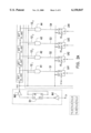
- FIG. 1 is a block diagram illustrating a device for generating a variable duty cycle clock according to the present invention
- FIGS. 2A through 2F are circuit diagrams illustrating a device for generating a variable duty cycle clock according to the present invention.
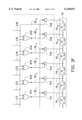
- FIG. 3 is a timing diagram showing all nodes of the device for generating a variable duty cycle clock as shown in FIG. 1 and FIG. 2.
- FIG. 1 is a block diagram illustrating a device for generating a variable duty cycle clock of the present invention
- FIG. 3 is a timing diagram illustrating all nodes of the device for generating a variable duty cycle clock as shown in FIG. 1.
- the device for generating a variable duty cycle clock includes a frequency divider 10, M-stage first delay elements 12, M-stage second delay elements 14, a selector 16 and a logic circuit 18.
- the frequency divider 10 receives an input clock CK and divided the input clock CK (by 2 in this case) to obtain a divided clock CK2. Therefore, the pulse width of the divided clock CK2 is just the period of the input clock CK.
- M-stage first delay elements 12 sequentially delay the divided clock CK2 for a first delay time t to obtain M first delay clocks 12 1 ⁇ 12 M .
- the clock 12 1 is obtained by delaying the divided clock CK2 for a first delay time t
- the clock 12 2 is obtained by delaying the clock 12 1 for a first delay time t (or by delaying the divided clock CK2 for two first delay times 2t)
- the clock 12 3 is obtained by delaying the clock 12 2 for a first delay time t (or by delaying the divided clock CK2 for three first delay times 3t)
- the clock 12 4 is obtained by delaying the clock 12 3 for a first delay time t (or by delaying the divided clock CK2 for four first delay times 4t), and so on.
- M-stage second delay elements 14 sequentially delay the divided clock CK2 for a second delay time ⁇ t to obtain M second delay clocks 14 1 ⁇ 14 M .
- ⁇ is a predetermined ratio (such as 1/2) which is used to define the duty cycle of the output clock
- the M second delay clocks 14 1 ⁇ 14 M correspond to the M first delay clocks 12 1 ⁇ 12 M respectively.
- the clock 14 1 is obtained by delaying the divided clock CK2 for a second delay time ⁇ t
- the clock 14 2 is obtained by delaying the clock 14 1 for a second delay time ⁇ t (or by delaying the divided clock CK2 for two second delay times 2 ⁇ t)
- the clock 14 3 is obtained by delaying the clock 14 2 for a second delay time ⁇ t (or by delaying the divided clock CK2 for three second delay times 3 ⁇ t)
- the clock 14 4 is obtained by delaying the clock 14 3 for a second delay time t (or by delaying the divided clock CK2 for four second delay times 4 ⁇ t), and so on.
- the selector 16 ANDs the divided clock CK2 and each of the M first delay clocks 12 1 ⁇ 12 M , respectively, to obtain M shrunk clock S 1 ⁇ S M .
- the M shrunk clock S 1 ⁇ S M correspond to the M first delay clocks 12 1 ⁇ 12 M , respectively, indicating the AND of the divided clock CK2 and each of the M first delay clocks 12 1 ⁇ 12 M .
- the first delay clock 12 x (say 12 8 ) corresponding to the shrunk clock S x will be exactly the inverse of the divided clock CK2, and the delay time of the first delay clock 12 x will be exactly the period of the input clock CK (or a half of the period of the divided clock CK2).
- the second delay clock 14 x (say 14 8 ) corresponding to the first delay clock 12 x will delay for the predetermined ratio of the delay time of the first delay clock 12 x , which is exactly the period of the input clock CK, to obtain a selected delay clock CK2'.
- the selector 16 In order to obtain the selected delay clock CK2', the selector 16 generates M control signals 16 1 ⁇ 16 M according to the M shrunk clocks S 1 ⁇ S M to control the M-stage second delay elements 14.
- control clock S x corresponding to the first delay clock 12 x is the only one that is all 1's to select the corresponding second delay clock 14 x , and all the other control clocks S 1 ⁇ S x-1 , S x+1 ⁇ S M are all 0's.
- the logic circuit 18 XORs the divided clock CK2 and the selected delay clock CK2' to output a clock CK' having a duty cycle of the predetermined ratio ⁇ .
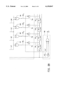
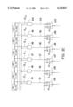
- FIGS. 2A through 2F are circuit diagrams illustrating a device for generating a variable duty cycle clock
- FIG. 3 is a timing diagram illustrating all nodes of the device for generating a variable duty cycle clock in FIG. 2.
- the M-stage first delay elements 12 are designed as 16-stage first delay elements
- the M-stage second delay elements 14 are designed as 16-stage second delay elements
- the duty ratio ⁇ of the input clock CK is adjusted to 1/2.
- the device for generating a variable duty ratio clock includes a frequency divider 10, 16-stage first delay elements 12, 16-stage second delay elements 14, a selector 16 and a logic circuit 18.
- the frequency divider 10 divides the input clock CK by two to obtain a divided clock CK2.
- the frequency divider 10 is constructed with a D-type flip flop which has a clock terminal (CLK) receiving the input clock CK inverted by an inverter IN1, a data terminal (D), an inverse output terminal (Qn) connected to the data terminal (D) and an output terminal (Q) generating the divided clock CK2.
- the 16-stage first delay elements 12 sequentially delay the divided clock CK2 for a first delay time t to obtain sixteen first delay clocks 12 1 ⁇ 12 16
- the 16-stage second delay elements 14 sequentially delay the divided clock CK2 for a second delay time ⁇ t to obtain sixteen second delay clocks 14 1 ⁇ 14 16
- the 16-stage first delay elements 12 are constructed with a delay line having sixteen first line segments connected in series, and each of the first line segments has the first delay time t.
- the 16-stage second delay elements 14 are constructed with a delay line having sixteen second line segments connected in series, and each of the second line segments has the second delay time ⁇ t.
- the sixteen first line segments sequentially delay the divided clock CK2 for the first delay time t to obtain the sixteen first delay clocks 12 1 ⁇ 12 16 .
- the sixteen second line segments sequentially delay the divided clock CK2 for the second delay time t to obtain the sixteen second delay clocks 14 1 ⁇ 14 16 .
- the ratio ⁇ of the second delay time ⁇ t to the first delay time t is set to 1/2. Therefore, the sixteen second delay clocks 14 1 ⁇ 14 16 have delay times half of those the sixteen first delay elements 12 1 ⁇ 12 16 , respectively.
- the selector 16 determines the period of the input clock CK according to the divided clock CK2 and the sixteen first delay clocks 12 1 ⁇ 12 16 .
- the selector 16 is constructed with sixteen AND gates A1 ⁇ A16, sixteen latch LA1 ⁇ LA16, fifteen XOR gates X1 ⁇ X15 and sixteen switches T1 ⁇ T16.
- the sixteen AND gates A1 ⁇ A16 respectively AND the divided clock CK2 and each of the sixteen first delay clocks 12 1 ⁇ 12 16 to obtain sixteen shrunk clocks S 1 ⁇ S 16 , indicating the ANDs of the divided clock CK2 and each of the sixteen first delay clocks 12 1 ⁇ 12 16 .
- the sixteen first delay clocks 12 1 ⁇ 12 16 are obtained by sequentially delaying for the first delay time t, the corresponding shrunk clocks S 1 ⁇ S 16 are also sequentially shrunk by the first delay time t.
- the first delay clock 12 x (say 12 8 ) corresponding to the shrunk clock S x is exactly the inverse of the divided clock CK2. That is to say, the delay time of the first delay clock 12 x , which is 8t, is exactly the period of the input clock CK (or a half of the period of the divided clock CK2).
- the sixteen latches LA1 ⁇ LA16 latch the sixteen shrunk clocks S 1 ⁇ S 16 , respectively, to obtain sixteen latch signals L 1 ⁇ L 16 .
- the sixteen latches LA1 ⁇ LA16 are triggered by falling edges of the divided clock CK2 to latch the sixteen shrunk clocks S 1 ⁇ S 16 .
- the latch signals L 1 ⁇ L x-1 (say L 1 ⁇ L 7 ) corresponding to the previous shrunk clocks S 1 ⁇ S x-1 (say S 1 ⁇ S 7 ) will become all 1's
- the latch signals L x ⁇ L 16 (say L 8 ⁇ L 16 ) corresponding to the shrunk clock S x (say S 9 ) and the preceding shrunk clocks S x+1 ⁇ S 16 (say S 9 ⁇ S 16 ) will become all 0's.
- the fifteen XOR gates X1 ⁇ X15 respectively XOR adjacent latch signals LA1 ⁇ LA16 to obtain fifteen select signals 16 1 ⁇ 16 15 .
- the select signal 16 x (say 16 8 ) obtained by XORing the latch signal L x and the latch signal L x+1 is all 1's, and all the other latch signals 16 1 ⁇ 16 x-1 (say 16 1 ⁇ 16 7 ) and 16 x+1 ⁇ 16 15 (say 16 9 ⁇ 16 16 ) are all 0's.
- the sixteen switches T1 ⁇ T16 are controlled by the fifteen select signals 16 1 ⁇ 16 15 from the fifteen XOR gates X1 ⁇ X15 and the latch signal L 16 from the latch LA16, respectively, to select the second delay clock 14 x according to the first delay clock 12 x as the selected delay clock CK2'.
- the delay time of the selected delay clock CK2' is just a half of the delay time of the first delay clock 12 x or a half of the period of the input clock CK.
- the logic circuit 18 XORs the divided clock CK2 and the selected delay clock CK2', the delay time of which is half the period of the input clock CK, to obtain a clock CK' having a 1/2 duty cycle.
- the device and method for generating a variable duty cycle clock of the present invention uses match delay lines to adjust the duty cycle, and uses digital circuits to lower the power dissipation.
- the device and method to generate a variable duty cycle clock of the present invention is portable and usable in different processes, and can improve response characteristics by reducing the oscillation time and the recovery time to less than one clock.
Landscapes
- Physics & Mathematics (AREA)
- Engineering & Computer Science (AREA)
- Theoretical Computer Science (AREA)
- Nonlinear Science (AREA)
- General Engineering & Computer Science (AREA)
- General Physics & Mathematics (AREA)
- Pulse Circuits (AREA)
Abstract
Description
Claims (12)
Applications Claiming Priority (2)
| Application Number | Priority Date | Filing Date | Title |
|---|---|---|---|
| TW88104223 | 1999-03-18 | ||
| TW88104223 | 1999-03-18 |
Publications (1)
| Publication Number | Publication Date |
|---|---|
| US6150847A true US6150847A (en) | 2000-11-21 |
Family
ID=21639987
Family Applications (1)
| Application Number | Title | Priority Date | Filing Date |
|---|---|---|---|
| US09/358,013 Expired - Lifetime US6150847A (en) | 1999-03-18 | 1999-07-21 | Device and method for generating a variable duty cycle clock |
Country Status (1)
| Country | Link |
|---|---|
| US (1) | US6150847A (en) |
Cited By (26)
| Publication number | Priority date | Publication date | Assignee | Title |
|---|---|---|---|---|
| US6201414B1 (en) * | 1999-10-28 | 2001-03-13 | Xerox Corporation | Pulse width modulation circuit |
| US20020093872A1 (en) * | 1999-10-29 | 2002-07-18 | Fujitsu Limited | Semiconductor integrated circuit, method of controlling the same, and variable delay circuit |
| US6639441B2 (en) * | 2001-01-19 | 2003-10-28 | Fujitsu Quantum Devices Limited | Clock signal correction circuit and semiconductor device implementing the same |
| US6654900B1 (en) * | 2000-04-19 | 2003-11-25 | Sigmatel, Inc. | Method and apparatus for producing multiple clock signals having controlled duty cycles by controlling clock multiplier delay elements |
| US6756833B2 (en) * | 2001-07-10 | 2004-06-29 | Renesas Technology Corp. | Delayed signal generation circuit |
| US20050184779A1 (en) * | 2004-02-19 | 2005-08-25 | Yoo Chang-Sik | Open-loop digital duty cycle correction circuit without DLL |
| US20060245130A1 (en) * | 2005-04-28 | 2006-11-02 | Sanyo Electric Co., Ltd. | Delay circuit |
| US20070252629A1 (en) * | 2006-05-01 | 2007-11-01 | Ibm Corporation | Method and apparatus for correcting the duty cycle of a digital signal |
| US20070255517A1 (en) * | 2006-05-01 | 2007-11-01 | Ibm Corporation | Method and apparatus for on-chip duty cycle measurement |
| US20070266285A1 (en) * | 2006-05-01 | 2007-11-15 | Ibm Corporation | Duty cycle measurement method and apparatus that operates in a calibration mode and a test mode |
| US20070271051A1 (en) * | 2006-05-01 | 2007-11-22 | Ibm Corporation | Method and apparatus for measuring the duty cycle of a digital signal |
| US20070271068A1 (en) * | 2006-05-01 | 2007-11-22 | Ibm Corporation | Method and Apparatus for Measuring the Relative Duty Cycle of a Clock Signal |
| US20080018373A1 (en) * | 2004-05-25 | 2008-01-24 | Zimlich David A | System and method for open-loop synthesis of output clock signals having a selected phase relative to an input clock signal |
| US20090112555A1 (en) * | 2006-05-01 | 2009-04-30 | International Business Machines Corporation | Design Structure For A Duty Cycle Measurement Apparatus That Operates In A Calibration Mode And A Test Mode |
| US20090125857A1 (en) * | 2007-11-12 | 2009-05-14 | International Business Machines Corporation | Design Structure for an Absolute Duty Cycle Measurement Circuit |
| US20090128133A1 (en) * | 2007-11-20 | 2009-05-21 | Boerstler David W | Duty Cycle Measurement Method and Apparatus for Various Signals Throughout an Integrated Circuit Device |
| US20090138834A1 (en) * | 2007-11-20 | 2009-05-28 | International Business Machines Corporation | Structure for a Duty Cycle Measurement Circuit |
| US20090167400A1 (en) * | 2007-12-26 | 2009-07-02 | Yusuke Tokunaga | Device and method for generating clock signal |
| EP2124338A1 (en) * | 2008-05-23 | 2009-11-25 | Sicon Semiconductor AB | Clock-signal generator |
| US7675336B1 (en) * | 2004-12-17 | 2010-03-09 | Altera Corporation | Clock duty cycle recovery circuit |
| US20110032015A1 (en) * | 2009-08-10 | 2011-02-10 | Qualcomm Incorporated | Systems and methods for clock correction |
| US7904264B2 (en) | 2007-11-12 | 2011-03-08 | International Business Machines Corporation | Absolute duty cycle measurement |
| US7902893B1 (en) | 2009-11-17 | 2011-03-08 | Zoran Corporation | Clock-signal generator |
| US9344066B2 (en) * | 2014-09-30 | 2016-05-17 | Texas Instruments Incorporated | Digital open loop duty cycle correction circuit |
| US9680363B2 (en) * | 2015-09-25 | 2017-06-13 | Intel Corporation | Low ripple mechanism of mode change in switched capacitor voltage regulators |
| JP2021048523A (en) * | 2019-09-19 | 2021-03-25 | 株式会社東芝 | Led drive control circuit, electronic circuit, and method for controlling led drive |
Citations (4)
| Publication number | Priority date | Publication date | Assignee | Title |
|---|---|---|---|---|
| US5410263A (en) * | 1992-05-28 | 1995-04-25 | Intel Corporation | Delay line loop for on-chip clock synthesis with zero skew and 50% duty cycle |
| US5506878A (en) * | 1994-07-18 | 1996-04-09 | Xilinx, Inc. | Programmable clock having programmable delay and duty cycle based on a user-supplied reference clock |
| US5852370A (en) * | 1994-12-22 | 1998-12-22 | Texas Instruments Incorporated | Integrated circuits for low power dissipation in signaling between different-voltage on chip regions |
| US5869978A (en) * | 1996-11-30 | 1999-02-09 | Daewoo Electronics Co., Ltd. | Circuit for removing noise components of oscillator |
-
1999
- 1999-07-21 US US09/358,013 patent/US6150847A/en not_active Expired - Lifetime
Patent Citations (4)
| Publication number | Priority date | Publication date | Assignee | Title |
|---|---|---|---|---|
| US5410263A (en) * | 1992-05-28 | 1995-04-25 | Intel Corporation | Delay line loop for on-chip clock synthesis with zero skew and 50% duty cycle |
| US5506878A (en) * | 1994-07-18 | 1996-04-09 | Xilinx, Inc. | Programmable clock having programmable delay and duty cycle based on a user-supplied reference clock |
| US5852370A (en) * | 1994-12-22 | 1998-12-22 | Texas Instruments Incorporated | Integrated circuits for low power dissipation in signaling between different-voltage on chip regions |
| US5869978A (en) * | 1996-11-30 | 1999-02-09 | Daewoo Electronics Co., Ltd. | Circuit for removing noise components of oscillator |
Cited By (48)
| Publication number | Priority date | Publication date | Assignee | Title |
|---|---|---|---|---|
| US6201414B1 (en) * | 1999-10-28 | 2001-03-13 | Xerox Corporation | Pulse width modulation circuit |
| US20020093872A1 (en) * | 1999-10-29 | 2002-07-18 | Fujitsu Limited | Semiconductor integrated circuit, method of controlling the same, and variable delay circuit |
| US6759884B2 (en) * | 1999-10-29 | 2004-07-06 | Fujitsu Limited | Semiconductor integrated circuit, method of controlling the same, and variable delay circuit |
| US6654900B1 (en) * | 2000-04-19 | 2003-11-25 | Sigmatel, Inc. | Method and apparatus for producing multiple clock signals having controlled duty cycles by controlling clock multiplier delay elements |
| US6639441B2 (en) * | 2001-01-19 | 2003-10-28 | Fujitsu Quantum Devices Limited | Clock signal correction circuit and semiconductor device implementing the same |
| US6756833B2 (en) * | 2001-07-10 | 2004-06-29 | Renesas Technology Corp. | Delayed signal generation circuit |
| US20050184779A1 (en) * | 2004-02-19 | 2005-08-25 | Yoo Chang-Sik | Open-loop digital duty cycle correction circuit without DLL |
| US7212055B2 (en) * | 2004-02-19 | 2007-05-01 | Hynix Semiconductor Inc. | Open-loop digital duty cycle correction circuit without DLL |
| US7688129B2 (en) * | 2004-05-25 | 2010-03-30 | Micron Technology, Inc. | System and method for open-loop synthesis of output clock signals having a selected phase relative to an input clock signal |
| US20080018373A1 (en) * | 2004-05-25 | 2008-01-24 | Zimlich David A | System and method for open-loop synthesis of output clock signals having a selected phase relative to an input clock signal |
| US7675336B1 (en) * | 2004-12-17 | 2010-03-09 | Altera Corporation | Clock duty cycle recovery circuit |
| US20060245130A1 (en) * | 2005-04-28 | 2006-11-02 | Sanyo Electric Co., Ltd. | Delay circuit |
| US7786775B2 (en) * | 2005-04-28 | 2010-08-31 | Sanyo Electric Co., Ltd. | Delay circuit |
| US20070271051A1 (en) * | 2006-05-01 | 2007-11-22 | Ibm Corporation | Method and apparatus for measuring the duty cycle of a digital signal |
| US20090112555A1 (en) * | 2006-05-01 | 2009-04-30 | International Business Machines Corporation | Design Structure For A Duty Cycle Measurement Apparatus That Operates In A Calibration Mode And A Test Mode |
| US7330061B2 (en) | 2006-05-01 | 2008-02-12 | International Business Machines Corporation | Method and apparatus for correcting the duty cycle of a digital signal |
| US7333905B2 (en) | 2006-05-01 | 2008-02-19 | International Business Machines Corporation | Method and apparatus for measuring the duty cycle of a digital signal |
| US7363178B2 (en) | 2006-05-01 | 2008-04-22 | International Business Machines Corporation | Method and apparatus for measuring the relative duty cycle of a clock signal |
| US20080174345A1 (en) * | 2006-05-01 | 2008-07-24 | Ibm Corporation | Method and apparatus for measuring the duty cycle of a digital signal |
| US7420400B2 (en) | 2006-05-01 | 2008-09-02 | International Business Machines Corporation | Method and apparatus for on-chip duty cycle measurement |
| US20070271068A1 (en) * | 2006-05-01 | 2007-11-22 | Ibm Corporation | Method and Apparatus for Measuring the Relative Duty Cycle of a Clock Signal |
| US7646177B2 (en) | 2006-05-01 | 2010-01-12 | International Business Machines Corporation | Design structure for a duty cycle measurement apparatus that operates in a calibration mode and a test mode |
| US20070266285A1 (en) * | 2006-05-01 | 2007-11-15 | Ibm Corporation | Duty cycle measurement method and apparatus that operates in a calibration mode and a test mode |
| US20070255517A1 (en) * | 2006-05-01 | 2007-11-01 | Ibm Corporation | Method and apparatus for on-chip duty cycle measurement |
| US20070252629A1 (en) * | 2006-05-01 | 2007-11-01 | Ibm Corporation | Method and apparatus for correcting the duty cycle of a digital signal |
| US7595675B2 (en) | 2006-05-01 | 2009-09-29 | International Business Machines Corporation | Duty cycle measurement method and apparatus that operates in a calibration mode and a test mode |
| US7617059B2 (en) | 2006-05-01 | 2009-11-10 | International Business Machines Corporation | Method and apparatus for measuring the duty cycle of a digital signal |
| US7904264B2 (en) | 2007-11-12 | 2011-03-08 | International Business Machines Corporation | Absolute duty cycle measurement |
| US8032850B2 (en) | 2007-11-12 | 2011-10-04 | International Business Machines Corporation | Structure for an absolute duty cycle measurement circuit |
| US20090125857A1 (en) * | 2007-11-12 | 2009-05-14 | International Business Machines Corporation | Design Structure for an Absolute Duty Cycle Measurement Circuit |
| US7917318B2 (en) * | 2007-11-20 | 2011-03-29 | International Business Machines Corporation | Structure for a duty cycle measurement circuit |
| US20090138834A1 (en) * | 2007-11-20 | 2009-05-28 | International Business Machines Corporation | Structure for a Duty Cycle Measurement Circuit |
| US20090128133A1 (en) * | 2007-11-20 | 2009-05-21 | Boerstler David W | Duty Cycle Measurement Method and Apparatus for Various Signals Throughout an Integrated Circuit Device |
| US7895005B2 (en) * | 2007-11-20 | 2011-02-22 | International Business Machines Corporation | Duty cycle measurement for various signals throughout an integrated circuit device |
| US20090167400A1 (en) * | 2007-12-26 | 2009-07-02 | Yusuke Tokunaga | Device and method for generating clock signal |
| US7782112B2 (en) * | 2007-12-26 | 2010-08-24 | Panasonic Corporation | Device and method for generating clock signal |
| EP2124338A1 (en) * | 2008-05-23 | 2009-11-25 | Sicon Semiconductor AB | Clock-signal generator |
| US20110032015A1 (en) * | 2009-08-10 | 2011-02-10 | Qualcomm Incorporated | Systems and methods for clock correction |
| WO2011019741A1 (en) * | 2009-08-10 | 2011-02-17 | Qualcomm Incorporated | Systems and methods for clock correction |
| US7902893B1 (en) | 2009-11-17 | 2011-03-08 | Zoran Corporation | Clock-signal generator |
| US9344066B2 (en) * | 2014-09-30 | 2016-05-17 | Texas Instruments Incorporated | Digital open loop duty cycle correction circuit |
| US9680363B2 (en) * | 2015-09-25 | 2017-06-13 | Intel Corporation | Low ripple mechanism of mode change in switched capacitor voltage regulators |
| CN107924217A (en) * | 2015-09-25 | 2018-04-17 | 英特尔公司 | Low ripple patterns of change mechanism in switched capacitor voltage adjuster |
| US9958922B2 (en) | 2015-09-25 | 2018-05-01 | Intel Corporation | Low ripple mechanism of mode change in switched capacitor voltage regulators |
| CN107924217B (en) * | 2015-09-25 | 2021-06-29 | 英特尔公司 | Low ripple mode change mechanism in switched capacitor voltage regulators |
| JP2021048523A (en) * | 2019-09-19 | 2021-03-25 | 株式会社東芝 | Led drive control circuit, electronic circuit, and method for controlling led drive |
| US20220117055A1 (en) * | 2019-09-19 | 2022-04-14 | Kabushiki Kaisha Toshiba | Led drive control circuitry, electronic circuitry, and led drive control method |
| US11706854B2 (en) * | 2019-09-19 | 2023-07-18 | Kabushiki Kaisha Toshiba | LED drive control circuitry, electronic circuitry, and LED drive control method |
Similar Documents
| Publication | Publication Date | Title |
|---|---|---|
| US6150847A (en) | Device and method for generating a variable duty cycle clock | |
| EP0660516B1 (en) | Digitally phase modulated clock exhibiting reduced rf emissions | |
| US5018169A (en) | High resolution sample clock generator with deglitcher | |
| US6292040B1 (en) | Internal clock signal generating circuit having function of generating internal clock signals which are multiplication of an external clock signal | |
| KR100459709B1 (en) | Serializer-deserializer circuit having enough set up and hold time margin | |
| US5920600A (en) | Bit phase synchronizing circuitry for controlling phase and frequency, and PLL circuit therefor | |
| US6262611B1 (en) | High-speed data receiving circuit and method | |
| US7466179B2 (en) | Phase interpolation circuit | |
| US5786715A (en) | Programmable digital frequency multiplier | |
| US5532633A (en) | Clock generating circuit generating a plurality of non-overlapping clock signals | |
| WO2002031980A2 (en) | Cyclic phase signal generation from a single clock source using current phase interpolation | |
| CA2201695A1 (en) | Phase detector for high speed clock recovery from random binary signals | |
| US5708381A (en) | Variable delay circuit | |
| JP3487533B2 (en) | Multiplier circuit and semiconductor integrated circuit device | |
| KR100344082B1 (en) | A pulse-duration modulation wave generating circuit | |
| US20020186808A1 (en) | Fully programmable multimodulus prescaler | |
| US6798266B1 (en) | Universal clock generator using delay lock loop | |
| US7061293B2 (en) | Spread spectrum clock generating circuit | |
| US6535989B1 (en) | Input clock delayed by a plurality of elements that are connected to logic circuitry to produce a clock frequency having a rational multiple less than one | |
| US5945861A (en) | Clock signal modeling circuit with negative delay | |
| US11646741B2 (en) | Pulse width modulator with reduced pulse width | |
| WO2002011278A1 (en) | Frequency synthesizer | |
| US4210776A (en) | Linear digital phase lock loop | |
| CA2017539A1 (en) | Method and apparatus for receiving a binary digital signal | |
| US20240039521A1 (en) | Fractional divider-calibrated phase modulator and interpolator for a wireless transmitter |
Legal Events
| Date | Code | Title | Description |
|---|---|---|---|
| AS | Assignment |
Owner name: VANGUARD INTERNATIONAL SEMICONDUCTOR CORPORATION, Free format text: ASSIGNMENT OF ASSIGNORS INTEREST;ASSIGNOR:LU, JR-HOUNG;REEL/FRAME:010124/0590 Effective date: 19990714 |
|
| STCF | Information on status: patent grant |
Free format text: PATENTED CASE |
|
| FPAY | Fee payment |
Year of fee payment: 4 |
|
| FPAY | Fee payment |
Year of fee payment: 8 |
|
| AS | Assignment |
Owner name: TAIWAN SEMICONDUCTOR MANUFACTURING CO., LTD, TAIWA Free format text: ASSIGNMENT OF ASSIGNORS INTEREST;ASSIGNOR:VANGUARD INTERNATIONAL SEMICONDUCTOR CORPORATION;REEL/FRAME:027560/0411 Effective date: 20111231 |
|
| FPAY | Fee payment |
Year of fee payment: 12 |