US6150866A - Clock supplying circuit and integrated circuit device using it - Google Patents
Clock supplying circuit and integrated circuit device using it Download PDFInfo
- Publication number
- US6150866A US6150866A US08/977,690 US97769097A US6150866A US 6150866 A US6150866 A US 6150866A US 97769097 A US97769097 A US 97769097A US 6150866 A US6150866 A US 6150866A
- Authority
- US
- United States
- Prior art keywords
- clock
- wiring
- circuit
- delay
- phase
- Prior art date
- Legal status (The legal status is an assumption and is not a legal conclusion. Google has not performed a legal analysis and makes no representation as to the accuracy of the status listed.)
- Expired - Lifetime
Links
Images


Classifications
-
- H—ELECTRICITY
- H03—ELECTRONIC CIRCUITRY
- H03K—PULSE TECHNIQUE
- H03K5/00—Manipulating of pulses not covered by one of the other main groups of this subclass
- H03K5/13—Arrangements having a single output and transforming input signals into pulses delivered at desired time intervals
- H03K5/131—Digitally controlled
-
- G—PHYSICS
- G06—COMPUTING; CALCULATING OR COUNTING
- G06F—ELECTRIC DIGITAL DATA PROCESSING
- G06F1/00—Details not covered by groups G06F3/00 - G06F13/00 and G06F21/00
- G06F1/04—Generating or distributing clock signals or signals derived directly therefrom
- G06F1/10—Distribution of clock signals, e.g. skew
-
- H—ELECTRICITY
- H03—ELECTRONIC CIRCUITRY
- H03K—PULSE TECHNIQUE
- H03K5/00—Manipulating of pulses not covered by one of the other main groups of this subclass
- H03K5/13—Arrangements having a single output and transforming input signals into pulses delivered at desired time intervals
- H03K5/133—Arrangements having a single output and transforming input signals into pulses delivered at desired time intervals using a chain of active delay devices
Definitions
- the present invention relates to a clock supplying circuit, and in particular relates to an internal clock supplying circuit in an integrated circuit device such as a synchronous DRAM that operates synchronised with an external clock.
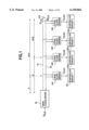
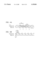
- FIG. 13 is a layout diagram of a synchronous DRAM.
- This memory 10 comprises: an address buffer 12 that latches address signals from outside, a decoder 14 that decodes the address signals, a driver 16 that drives a word line in accordance with the decoder output, a memory cell region 18, sense amplifier 20, bit selection circuit 22 and a plurality of output buffers 24-27.
- output buffers 24-27 are supplied with internal clock I CLK and output data with the timing of this clock.
- a DLL (Delayed Lock Loop) circuit 30 is provided within the memory to align this output timing with the timing of the external clock E CLK supplied from the system.
- This DLL circuit 30 inputs the external clock E CLK and generates an internal clock I CLK taking into account the propagation delay time resulting from the resistance R1 and capacitance C of wiring 32 through which the internal clock signal is propagated.
- an internal clock I CLK whose phase coincides with that of external clock E CLK is supplied to output buffers 24-27.
- a number of address buffer circuits 12 corresponding to the number of address signals.
- the internal clock phases supplied to the respective address buffer circuits are still offset.
- the same problem of skewing of the internal clock occurs likewise in effecting synchronisation at an arbitrary position in an integrated circuit such as for example a logic circuit or microprocessor in addition to memory.
- Methods of eliminating this skewing of the internal clock include adopting a tree structure for the wiring from the clock driver and matching the timings at respective positions where the internal clock is supplied, or making the wirings whereby the clock is supplied all of the same length. However, all of these necessitate excess wiring and so constitute a factor lowering spatial efficiency.
- an object of the present invention is to solve the aforementioned problems and to provide a clock supplying circuit wherein skewing of the internal clock at an arbitrary position in the integrated circuit can be eliminated.
- a further object of the present invention is to provide a clock supplying circuit and an integrated circuit device employing this wherein skewing of the internal clock dependent on the position in which an internal circuit is arranged can be eliminated, when an internal circuit arranged at an arbitrary position in the integrated circuit is operated in synchronism with an internal clock.
- Another object of the present invention is to provide a clock supplying circuit that is capable of supplying an internal clock to a plurality-of internal circuits with the same timing without dependence on the arrangement of this plurality of internal circuits.
- a clock supplying circuit that supplies a clock to a plurality of controlled circuits arranged in respectively different positions, comprising:
- a main clock drive circuit for outputting a first clock to the forward wiring of the forward and backward wiring and for outputting a second clock whose period is shorter than the first clock to the internal clock supply wiring;
- a plurality of local clock drive circuits arranged, in the respective vicinities of the controlled circuits, being supplied with a forward clock propagated by the first clock along the forward wiring and with a back clock propagated along the backward wiring of the forward and backward wiring, and being also supplied with the second clock propagating along the internal clock supply wiring, for delaying the phase of the supplied second clock so as to coincide with a phase intermediate the forward clock and the back clock, and for supplying the delayed clock of the second clock to the respectively corresponding controlled circuits as local clock.
- the local clocks are generated having a phase intermediate that of the forward clock and the back clock for phase comparison, so, irrespective of the positions of the local clock drive circuits, the phases of the plurality of local clocks can be made to coincide.
- a clock having the aligned phase can therefore be supplied to a plurality of controlled circuits arranged in different positions in an integrated circuit device.
- first and second forward and backward wirings a first and second group of controlled circuits, and first and second local clock drive circuits that supply local clocks to the controlled circuits each of which are arranged along the respective forward and backward wirings, while the main clock drive circuit outputs a first clock to the forward wirings of the first and second forward and backward wirings.
- a forward and backward wiring delay circuit on the second forward and backward wiring. The delay time of this forward and backward wiring delay circuit is controlled such that the phases of the two back clocks that are propagated along the first and second backward wirings coincide.
- first and second local clock drive circuits arranged in the first and second controlled circuit groups can generate local clocks that have the same timing.
- the flexibility of arrangement of the main clock drive circuit and the local clock drive circuits can consequently be increased.
- FIG. 1 is a diagram of a clock supplying circuit according to an embodiment of the present invention
- FIG. 2 is a diagram given in explanation of the timing of a local clock in FIG. 1;
- FIG. 3 is a diagram of a clock supplying circuit according to a second embodiment of the present invention.
- FIG. 4A and 4B are diagrams given in explanation of the periods of forward clock F CLK and back clock B CLK ;
- FIG. 5 is a diagram showing an example layout of a local clock drive circuit
- FIG. 6 is a circuit diagram of delay circuits 70, 71, 72 of a local clock drive circuit
- FIG. 7 is a circuit diagram of a shift register 60 of a local clock drive circuit
- FIG. 8 is a detail circuit diagram of a phase comparison circuit 50 of a local clock drive circuit
- FIG. 9 is a timing chart illustrating the operation of a phase comparison circuit
- FIG. 10 is a diagram showing an example of a synchronous DRAM utilising a clock supplying circuit
- FIG. 11 is a diagram of a circuit layout of a main clock drive circuit
- FIG. 12 is a diagram showing a further example layout of a main clock drive circuit
- FIG. 13 is a diagrammatic circuit layout of a synchronous DRAM
- FIG. 14 is an overall layout diagram of a third embodiment
- FIG. 15 is a detail circuit diagram of FIG. 14;
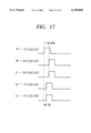
- FIG. 16 is a diagram given in explanation of the operation of phase comparison circuit 869 and variable-delay circuit 828 of FIG. 15;
- FIG. 17 is a timing chart given in explanation of the operation of phase comparison circuit 869 and variable-delay circuit 828 of FIG. 15;
- FIG. 18 is a timing chart of the operation of a main DLL
- FIG. 19 is a diagram illustrating an example circuit diagram of a frequency divider 840.
- FIG. 20 is a specific circuit diagram of a dummy delay circuit 866
- FIG. 21 is a timing chart of a dummy delay circuit 866
- FIG. 22 is a diagram showing a fourth embodiment
- FIG. 23 is a diagram showing a fifth embodiment.
- FIG. 24 is a diagram showing a sixth embodiment.
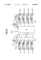
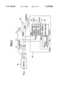
- FIG. 1 is a view of a clock supplying circuit according to an embodiment of the present invention.
- the present embodiment comprises a main clock drive circuit 40 and local clock drive circuits 441-444 provided in the vicinity of controlled circuits 451-454 within the integrated circuit.
- Forward wiring 41 and backward wiring 42 are arranged along local clock drive circuits 441-444.
- a clock from main clock drive circuit 40 is supplied on forward wiring 41 and this clock is returned at the extremity of forward wiring 41 and propagated through backward wiring 42. Accordingly, the clock on forward wiring 41 will be called forward clock F CLK and the clock on backward wiring 42 will be called back clock B CLK .
- the forward clock F CLK and back clock B CLK are supplied to each of local clock drive circuits 441-444 from forward and backward wiring 41 and 42 at the positions in the vicinity of the respective circuits, and local clocks L CLK1 -L CLK4 with timing intermediate that of forward clock F CLK and back clock B CLK are generated by respective local clock drive circuits. That is, the phases of the local clocks in all cases match the phase of forward clock F CLK at the extremity 410 of forward wiring 41.
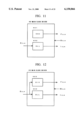
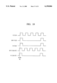
- FIG. 2 is a view given in explanation of the timing of the local clocks of FIG. 1.
- FIG. 2 the timing of forward clock F CLK and back clock B CLK and the timing of local clock L CLK at local clock drive circuits 441-444 are respectively shown.
- forward clock F CLK generated by main clock drive circuit 40 is input to local clock drive circuit 441 at the timing of time point t1.
- back clock B CLK is input at the timing of time point 2td-t1.
- td is the time required for the clock to propagate along forward wiring 41.
- the period from time point 0 to time point 2td indicates the time taken by the clock to be propagated through forward wiring 41 and backward wiring 42.
- Local clock drive circuit 441 generates a local clock of timing:
- local clock drive circuit 442 generates a local clock of timing:
- the timings of the local clocks generated in local clock drive circuits 443 an d 444 are respectively:
- the timings of all the local clocks I CLK1 -I CLK4 are therefore a time point td irrespective of their position.
- forward wiring 41 and backward wiring 42 are merely arranged along the local clock drive circuits from the main clock drive circuit 40: this layout does not lower wiring efficiency.
- respective local clocks L CLK1 -L CLK4 are supplied to controlled circuits 451-454 so that these controlled circuits are operated with identical timing.
- main clock drive circuit 40 corresponds to DLL circuit 30 which is supplied with external clock E CLK
- the controlled circuits respectively correspond to the output buffers.
- main clock drive circuit 40 corresponding to DLL circuit 30 generates a clock such that the timings of operation of each controlled circuit coincide with the timing (time point td) at which forward clock F CLK reaches the extremity 410 of forward wiring 41.
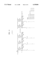
- FIG. 3 is a diagram of a clock supplying circuit according to a second embodiment of the present invention.
- an internal clock I CLK is generated by main clock drive circuit 40.
- internal clock wiring 43 is added.
- forward clock F CLK and back clock B CLK have a longer period than internal clock I CLK .
- the period of the forward clock and back clock are set to more than 2td, which is the time for propagation along forward wiring 41 and backward wiring 42.
- the period of the H level or L level of the forward clock or back clock is set to more than the time 2td for propagation along forward wiring 41 and backward wiring 42.
- FIG. 4 is a diagram given in explanation of the periods of forward clock F CLK and back clock B CLK .
- FIG. 4A shows a timing chart of the case where the forward clock and back clock have practically the same period as internal clock I CLK Internal clock I CLK has the same short period as the external clock for ordinary high-speed operation. For example, in the case of FIG. 4A, this period is 4 nsec. In this case, assuming that the delay time produced by wirings 41 and 42 exceeds this period of 4 nsec, it is difficult for a local clock drive circuit that is supplied with both clocks F CLK and B CLK to identify whether back clock B CLK has a delay of "a” shown in FIG. 4A with respect to forward clock F CLK , or has a delay of "b", or has a delay of "c” or "d".
- the period of forward clock F CLK and back clock B CLK are set to be longer than internal clock I CLK Internal clock I CLK has the same short period as external clock E CLK , to make possible high-speed operation.
- the period of forward clock F CLK and back clock B CLK is set to the long period of 32 nsec. Consequently, as shown at "b" of FIG. 4A, even if back clock B CLK is 5 nsec delayed from forward clock F CLK , since this delay is within 32 nsec, the local drive circuit can easily detect the difference of these two delay times.
- This forward clock and back clock could be generated by frequency division of external clock E CLK , or could be generated by an oscillating circuit independently of the external clock.
- FIG. 11 is a diagram showing an example layout of a main clock drive circuit 40.
- a DLL circuit 402 that generates an internal clock I CLK of the phase described above from external clock E CLK and an oscillating circuit 401 that generates a forward clock F CLK independent of external clock E CLK .
- FIG. 12 is a diagram showing a further example layout of main clock drive circuit 40.
- a DLL circuit 402 that generates an internal clock I CLK of the phase described above from external clock E CLK and a frequency division circuit 403 that generates a forward clock F CLK by frequency division of external clock E CLK .
- the length of the H level of the forward clock and back clock are set to be longer than the delay time 2td of clock wirings 41 and 42.
- the delay times of the two clocks can be sampled with a timing where the H levels of the two clocks overlap. The same effect can therefore be anticipated as in the case where the length of the L levels of the two clocks is set to be longer than 2td.
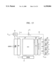
- FIG. 5 is a diagram showing an example layout of a local clock drive circuit according to the second embodiment.
- main clock drive circuit 40 is supplied with external clock E CLK and generates internal clock I CLK and the forward clock F CLK such that the timing at which the clock arrives at the extremity 410 of the wiring and the external clock E CLK are synchronised.
- Local clock drive circuit 441 comprises a phase comparison circuit 50, shift register 60 as a delay controller and delay circuits 70, 71, and 72.
- First delay circuit 70 is supplied with internal clock I CLK and outputs local clock L CLK that has been subjected to a prescribed time delay.
- second and third delay circuits 71 and 72 are supplied with forward clock F CLK and output a clock FD CLK having a delay time that is twice the delay time of the first delay circuit 70.
- Phase comparison circuit 50 compares the phase of this clock FD CLK and back clock B CLK . This phase comparison result is supplied to shift register 60 and shift register 60 controls the delay time of the three delay circuits 70, 71 and 72.
- local clock drive circuit 441 is assumed to be driver circuit 441 at the left end in FIG. 3, the delay times of the first to the third delay circuits 70, 71, 72 are all controlled to (td-t1).
- a local clock L CLK is obtained by delaying the internal clock I CLK by (td-t1). Since internal clock I CLK already has a delay of t1, local clock L CLK has a delay of td from the output stage of main DLL 402. This is the timing with which extremity 410 is reached.
- clock FD CLK is a clock obtained by delaying forward clock F CLK by 2(dt-t1). As described with reference to FIG. 2, clock FD CLK having this delay is a clock which is synchronised in phase with back clock B CLK .
- phase comparison circuit 50 detects which of back clock B CLK and clock FD CLK , which is delayed by 2(td-t1) from forward clock F CLK , is leading in phase, or whether their phases are the same.
- the control value of shift register 60 is controlled by these detection signals A-D, and the delay time of delay circuits 70-72 is controlled in accordance with this control value.
- the phase of clock FD CLK and back clock B CLK are controlled to coincide.
- Outputs A-D of phase comparison circuit 50 are detection signals indicating the phase comparison result which is output in accordance with the phase difference between clock FD CLK and back clock B CLK .
- signals A, B are signals that detect the phase of clock FD CLK is lagging with respect to back clock B CLK .
- the control value of the shift register is controlled in response to these signals A, B to a value such as to make the delay time of the delay circuit shorter; as a result, the phases of clock FD CLK and local clock L CLK are speeded up.
- signals C, D are signals that detect the phase of clock FD CLK is leading that of back clock B CLK .
- the control value of the shift register is controlled in response to these signals C, D to a value such as to prolong the delay time of the delay circuit; as a result, the phases of clock FD CLK and local clock L CLK are slowed down.
- detection signals A-D are all L level. In this way, local clock L CLK always has a phase intermediate that of forward clock F CLK and back clock B CLK .
- first delay circuit 70 can be eliminated from the example of FIG. 5 and the output of second delay circuit 71 used as local clock L CLK .
- FIG. 6 is a circuit diagram showing an example of delay circuits 70, 71, 72 of a local clock drive circuit.
- Delay circuits 70, 71, 71 have the same circuit construction. Their delay times are selected by control signals p1-p(n). These delay circuits output the clock that is applied at input terminal IN at output terminal OUT with a prescribed time delay.
- there are n delay circuit stages the first stage being constituted by NANDs 711, 712 and inverter 713, the second stage being constituted by NANDs 721, 722 and inverter 723 and likewise hereinbelow the n-th stage being constituted by NANDs 761, 762 and 763.
- control signals p1-p(n) is H level, while all the others are L level.
- the corresponding NAND 711, 721, . . . 761 is then opened by the control signal p that has become H level, so that the applied clock at the input IN is passed.
- the other NANDs 711, 721, . . . 761 corresponding to control signals p of L level are closed.
- NAND 711 is opened when control signal p1 is H level, with the result that a delay path is formed from input terminal IN to output terminal OUT through inverter 701, NANDs 711 and 712 and inverter 713. A delay of four gate stages is therefore provided.
- control signal p2 When control signal p2 is H level, NAND 721 is opened. Since the input of gate 762 is also H level, the output of inverter 763 is H level and likewise the outputs of inverters 753, 743 . . . are H level. Consequently, NAND 722 is also in opened condition. As a result, a delay path is formed from input terminal IN to output terminal OUT through inverter 701 and gates 721-723, 712, 713. Consequently, a delay of six gate stages is provided.
- FIG. 7 is a circuit diagram of the shift register 60.
- part of the shift register is shown and, for convenience in description, control signals p1-p6 of the delay circuits are shown.
- Detection signals A-D from phase comparison circuit 50 are supplied to this shift register 60: the H-level control signal p is shifted to the right by signals A, B and H-level control signal p is shifted to the left by signals C, D.
- Each stage of shift register 60 respectively comprises a latch circuit including, for example in the first stage, NAND gate 612 and inverter 613. Also, it comprises transistors 614, 615 that forcibly invert the condition of latch circuits 612, 613 in response to detection signals A-D. Transistors 616, 617 are provided in order to ensure that latch circuits not to be the subject of inversion are not inverted by transistors 614, 615.
- the layout of the circuits of the second to sixth stages is identical. All these transistors are N-channel transistors.
- the fourth-stage output p4 is in H level condition.
- the other output are all in L level condition.
- the condition of the latch circuits of each stage is indicated in FIG. 7 by H or L.
- the NAND (612, 622, 632) output is H level and the inverter (613, 623, 633) output is L level
- the NAND (642, 652,662) output is L level while the inverter (643, 653, 663) output is H level.
- the transistors that are connected to ground 617, 627, 637, 647, 646, 656 and 666 respectively are therefore in conductive condition.
- transistor 647 in the fourth stage circuit and transistor 636 in the third stage circuit which are on both sides of the boundary in respect of latching condition, are in conductive condition, and their latch condition is a condition that can be inverted in response to detection signal B or C.
- transistor 645 conducts, so that the output of inverter 643 is forcibly driven from H level to L level.
- the output of NAND gate 642 is also changed over from L level to H level and this condition is latched. Since the output of NAND gate 642 becomes H level, the output p4 of NOR gate 641 becomes L level and, in turn, due to change in the output of inverter 643 to L level, the output p5 of NOR gate 651 is changed over to H level.
- the H-level control signal shifts from p4 to p5. As described with reference to FIG. 6, with shifting of the H-level control signal p leftwards, the delay path of the delay circuit becomes longer and the delay time is controlled to be longer.
- detection signals A, B control a rightwards shift of H-level output and detection signals C, D control a leftwards shift of H-level output.
- detection signals A and D effect shift control when outputs p1, p3 or p5 are H level
- detection signals B, C effect shift control when outputs p2, p4, p6 are H level.
- FIG. 8 is a detailed circuit diagram of phase comparison circuit 50.
- This phase comparison circuit 50 has a phase detection section 51 that detects the relationship of the phases of the two clocks, namely, of input terminal In, which is supplied with the clock FD CLK , and reference clock terminal RefCLK, which is supplied with back clock B CLK .
- This phase detection circuit 51 has two latch circuits and detects the conditions: (1) where the phase of clock FD CLK leads that of back clock B CLK by more than a fixed time; (2) where the phase of clock FD CLK is in a phase difference relationship within a fixed time with respect to back clock B CLK , and (3) when the phase of clock FD CLK lags back clock B CLK by more than a fixed time.
- the above three conditions are detected by a combination of detection outputs n1-n4.
- Sampling pulse generating section 52 outputs a sampling signal to node n9 when the two clocks B CLK and FB CLK are both H level.
- Sampling latch circuit section 53 samples detection outputs n1-n4 by means of sampling gates 508-511 under the control of sampling signal n9, and latches these by means of a latch circuit consisting of NANDs 512, 513 and 514, 515. The detection outputs n1-n4 on sampling are therefore respectively latched in nodes n5-n8.
- Divide-by-2 frequency divider circuit 54 detects when both clocks FD CLK and B CLK are H level by means of NAND gate 520 and divides this detection pulse n10 in frequency by a factor of 2, to generate inverse-phase pulse signals n11 and n12.
- Decoder section 55 decodes the signals that have been sampled and latched at nodes n5-n8 and, if clock FD CLK leads reference clock B CLK , makes the output of diode 536 H level; if the phases of both clocks coincide, it makes the outputs of diodes 536 and 540 both L level; and if clock FD CLK lags clock B CLK , it makes the output of diode 540 H level.
- output circuit section 56 outputs detection signals A-D in response to inverse-phase pulse signals n11 and n12.
- Detection signals A-D control the condition of shift register 60 as already described.
- FIG. 9 is a timing chart showing the operation of FIG. 8.
- This FIG. 9 shows, in order, the condition in which clock FD CLK leads back clock B CLK , the condition in which the phases of both clocks coincide, and the condition in which clock FD CLK lags back clock B CLK .
- sampling pulse n9 is S1 or S2
- clock FD CLK is leading, so this is detected and detection signal C is output with H level in response to pulse n12
- detection signal D is output with H level in response to pulse nil.
- the sampling pulse is S3
- the phases coincide and detection signals A-D are all L level.
- sampling pulses S4, S5, S6, clock FD CLK lags so this is detected and detection signal B in response to pulse n11 or detection signal A in response to pulse n12 respectively become H level.
- a sampling pulse n9 having a width corresponding to the delay time of delay circuit 506 is generated from the timing with which the two clocks FD CLK , B CLK both become H level, the latch condition in phase comparison section 51 is sampled, and this latch condition is latched by latch section 53. That is, the condition of nodes n1-n4 is transferred to nodes n5-n8.
- Pulse n10 is then generated with the timing at which both clocks FD CLK and B CLK become H level.
- the latch circuits of NANDs 524, 525 and the latch circuits of NANDS 528, 529 are coupled by gates 526, 527 and gates 530, 531, these gates being opened by an inverting and non-inverting pulse of pulse n10. Consequently, pulse n10 is divided in frequency by a factor of 2.
- decoder section 55 in response to the H, L, H, L level condition of nodes n5-n8, the output of inverter 538 becomes H level and the output of inverter 540 becomes L level. Consequently, in response to pulse n12, H level of inverter 536, through NAND 543 and inverter 544, makes detection signal C become H level. In response to the H level of detection signal C, the H level output of the shift register is shifted to the left and the delay path of delay circuits 71, 72, 73 becomes longer. As a result, clock FD CLK is controlled in the lagging direction.
- phase comparison section 51 it is detected by phase comparison section 51 that clock FD CLK is leading, and so that the detection signal D becomes H level in response to pulse n11. Consequently, in the same way, the H-level output of shift register 60 shifts to the left, increasing the length of the delay path of delay circuits 71, 72, 73.
- n1 H
- n2 L
- n3 L
- n4 H
- n5 H
- n6 L
- n7 L
- n8 H
- n1 L
- n2 H
- n3 H
- n4 L
- n5 L
- n6 H
- n7 H
- n8 L
- phase comparison section 51 becomes:
- This condition is decoded by decoder section 55 and results in L level output of inverter 536 and H-level output of inverter 540.
- the detection signals B and A therefore respectively become H level in response to pulse n11 and n12.
- the output p of shift register 60 is shifted rightwards, shortening the delay path of delay circuits 71, 72, 73 and so shortening the delay time.
- clock FD CLK is controlled in the advancing direction.
- phase comparison circuit 50 As described above, by means of the closed loop of phase comparison circuit 50, shift register 60, delay circuits 72, 73 and clock FD CLK , the phase of local clock L CLK is controlled to a timing intermediate that of forward clock F CLK and back clock B CLK .
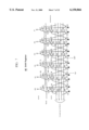
- FIG. 10 is a diagram showing an example of a synchronous DRAM utilising the clock supplying circuit described above.
- local clock L2 CLK is supplied to a plurality of output buffers 24-29 and local clock L1 CLK is further supplied to a plurality of address buffers 121-124.
- an address buffer clock supplying circuit and an output buffer clock supplying circuit For the address buffers, main DLL circuit 401 and forward wiring 411, backward wiring 421 and internal clock wiring 431 are arranged along address buffers 121-124, while local clock drive circuits 441-444 are arranged in the vicinity of the respective address buffers 121-124.
- the respective local clock drive circuits 441-444 are supplied with forward clock F CLK , back clock B CLK and internal clock I1 CLK , and, as described above, a local clock L1 CLK is generated having a phase of timing intermediate that of forward clock F CLK and back clock B CLK .
- Main DLL circuit 401 generates an internal clock I1 CLK such that the address buffers can uniformly accept and latch address signals A1-A4 at the time when the clock reaches the extremity 4210.
- the respective local clocks L1 CLK have phases that coincide with the timing at which the internal clock reaches extremity 4210.
- main DLL circuit 402 and forward wiring 412, backward wiring 422 and internal clock wiring 432 are arranged along output buffers 24-27, and local clock drive circuits 445-448 are arranged in the vicinity of the respective output buffers 24-27.
- the respective local clock drive circuits 445-448 are supplied with forward clock F CLK F back clock B CLK and internal clock I2 CLK and, as described above, local clock L2 CLK is generated with a timing intermediate that of forward clock F CLK and back clock B CLK .
- a clock supplying circuit according to the present invention can be widely applied to various types of circuit apart from the above in which synchronisation is to be obtained at a plurality of positions.
- forward and backward wiring is provided from the main clock drive circuit along the circuits to be controlled and local clock drive circuits are provided in the vicinity of these controlled circuits; a local clock having a phase intermediate that of the forward clock and back clock is then generated and supplied to the controlled circuits, so all the respective controlled circuits can be operated with the same timing, and the problem of skewing of the control clock can be avoided.
- the phase difference of the forward clock and back clock can be more easily detected.
- the phase difference can-be easily detected if, preferably, the forward clock and back clock have a period equal to or longer than the back-and-forth delay time of the wiring, so that the phase difference of the two clocks is always less than 1 period.
- the clock supplying circuit of the present invention is not restricted to synchronous DRAMS, but can be widely applied to integrated circuit devices.
- a forward clock and back clock were applied to local DLLS arranged respectively in the vicinity of controlled circuits arranged in one direction with respect to a main DLL corresponding to the main clock drive circuit, and the local DLLs generated local clocks L CLK synchronised with the timing at the furthest extremity of the forward and backward clock wiring.
- the main DLL and a plurality of local DLLs are arranged in an actual integrated circuit, it is not necessarily essential that the main DLL should be arranged at one end while the plurality of local DLLs are arranged on one side of it. Instead, space for providing a main DLL may be reserved at any desired position of the plurality of local DLLS. Since the local DLLs are arranged in the vicinity of controlled circuits such as output circuits and/or input circuits, they are disposed in positions dependent on the layout of the output electrodes and/or input electrodes of the integrated circuit device. The space for arranging the main DLL will therefore be different, case-by-case. The present embodiment enables local DLLs arranged on both sides of the main DLL to generate local clocks of identical phase irrespective of the location in which the main DLL and controlled circuit are arranged.
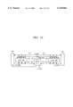
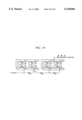
- FIG. 14 is an overall layout diagram of a third embodiment.
- a main DLL 821 is arranged at an arbitrary position of a plurality of output buffers OB, and on both sides of it, there are arranged a plurality of output buffers and local DLL groups 830, 831 corresponding thereto.
- a forward clock F-CLK is supplied to left and right forward clock wirings 824, 825, and back clocks B-CLK1, B-CLK2 are returned from both extremities through left and right backward clock wirings 827, 829.
- forward clock wiring 824 and backward clock wiring 827 on the right side of main DLL 821 are fairly long in comparison with the corresponding wirings 825, 829 on the left-hand side, or are in circumstances of large load capacity etc.
- the time required for clock F-CLK to travel back-and-forth along the right side wirings 824, 827 of main DLL 821 is longer than the time required for it to travel back-and-forth along the left-side wirings 825, 829.
- a fixed delay circuit 826 is provided on for example the right-hand side back-and-forth wiring 824, 827 so as to continually generate a fixed delay time.
- a variable-delay circuit 828 is provided on the left-hand side back-and-forth wiring 825, 829 so that the timing with which the left-hand back clock B-CLK2 is returned can be made to coincide with the timing with which the right-hand back clock B-CLK1 is returned.
- main DLL 821 includes a phase comparison circuit that compares the phases of the two back clocks B-CLK1 and B-CLK2. Based on the result of the phase comparison by this phase comparison circuit, the delay time of the variable-delay circuit 828 is controlled such that the phases of the two back clocks B-CLK1, B-CLK2 coincide.
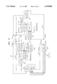
- FIG. 15 is a detail circuit diagram of FIG. 14.
- Local DLLs 441 have the same construction as in FIG. 5.
- a fixed delay circuit 826 is arranged at the furthest extremity of forward clock wiring 824 while a variable-delay circuit 828 is arranged at the furthest extremity of the other backward clock wiring 829.
- Main DLL 821 is also provided with a phase comparison circuit 869 that detects the phase difference of the two back clocks B-CLK1, B-CLK2.
- variable delay circuit 828 There is further provided for variable delay circuit 828 a shift register 832 that is controlled by the output 870 of phase comparison circuit 869.
- This shift register 832 has a delay control function that controls the variable delay circuit 828: it controls the delay time of variable delay circuit 828 in accordance with the output 870 of phase comparison circuit 869 such that the phases of the two back clocks B-CLK1 and B-CLK2 coincide.
- Phase comparison circuit 869, shift register 823 and variable delay circuit 828 have a similar circuit construction to phase comparison circuit 50, shift register 60 and variable delay circuit 70 described in the first and second embodiments. Their operation is also similar.
- right-hand side back clock B-CLK1 passed through the fixed delay circuit 826 is supplied at the reference clock terminal Ref-CLK of the phase comparison circuit 50 shown in FIG. 8, while left-hand side back clock B-CLK2 passed through variable-delay circuit 828 whose delay is controlled is supplied to input terminal in of the phase comparison circuit 50.
- Comparison result signals A, B, C, D obtained by detecting the phase relationship of the two back clocks are generated as output 870.
- phase comparison result signals A, B are generated when back clock B-CLK2 is delayed; shift register 832 supplies a delay control signal in response to the signals A, B such as to shorten the delay time of variable-delay circuit 828.
- phase comparison result signals C, D are generated when back clock B-CLK2 is leading; shift register 832 supplies a delay control signal in response to these signals C, D such as to extend the delay time of variable delay circuit 828.
- variable delay circuit 828 By controlling the delay time of variable delay circuit 828 as described above such that the phases of the two back clocks B-CLK1 and 2 coincide, the phases of the local clocks L CLK generated by the local DLLs arranged on both sides of main DLL 821 can all be made to coincide independent of the position of main DLL 821 or the load capacity etc. of the clock wiring.
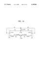
- FIG. 16 is a view given in explanation of the operation of phase comparison circuit 869 and variable delay circuit 828 of FIG. 15.
- FIG. 17 is a timing chart of this.
- the phases of back clocks B-CLK1, B-CLK2 coincide at the position N821 of main DLL 821. These clock periods are longer, with the provision of a margin, than the time required for their travel the forward and backward wirings, with frequency division. The times required for the two clocks B-CLK1, B-CLK2 to travel the forward and backward wiring are therefore controlled to be the same.
- the local clocks generated by the local DLLs located to the right of the main DLL are controlled to the timing with which the forward clock F-CLK passes through the furthest extremity N826 on the right-hand side of the forward and backward wirings 824, 827.
- Node N826 is an intermediate point of fixed delay circuit 826.
- the local clocks generated by the local DLLs arranged on the left-hand side of the main DLL are controlled to the timing with which the forward clock F-CLK passes through the position of the furthest extremity N828 of the forward and backward wirings 825, 829 on the left-hand side.
- Node N828 is an intermediate point of variable delay circuit 828.
- the time required for back clocks B-CLK1, B-CLK2 to travel forward and backward wirings is assumed to be 2TA, the timing which the clocks pass through nodes N826, N828 lags the forward clock F-CLK-821 generated by main DLL 821 by a time TA.
- FIG. 15 shows the detailed construction of main DLL 821.
- Main DLL 821 generates forward clock F-CLK and an internal clock INT-CLK that is synchronised with a reference clock such as external clock E-CLK or a clock lagging the external clock by a prescribed phase (for example 120° etc.) (hereinbelow referred to simply as external clock E-CLK).
- a reference clock such as external clock E-CLK or a clock lagging the external clock by a prescribed phase (for example 120° etc.) (hereinbelow referred to simply as external clock E-CLK).
- the two clocks INT-CLK, F-CLK are generated so as to have a phase leading by an amount corresponding to the time TA required for one-way travel of the forward and backward wiring from the external clock E-CLK, which is the reference clock.
- main DLL 821 comprises: frequency divider 840 that effects frequency division of the external clock (reference clock); phase comparison circuit 874 that compares the phases of the output DIV-CLK of the frequency divider and a delayed clock D-CLK obtained by delaying forward clock F-CLK by an amount corresponding to the time TA required for one-way travel along the forward and backward wiring; a shift register 831 that is supplied with the phase comparison result signal 875 generated by phase comparison circuit 874; and variable delay circuits 833, 865.
- Internal clock INT-CLK is output by applying external clock E-CLK to variable-delay circuit 833.
- forward clock F-CLK is output by applying the clock DIV-CLK obtained by frequency division performed by frequency divider 840 to variable-delay circuit 865.
- Dummy delay circuit 866 generates the delay time TA required for one-way travel of the forward and backward wiring.
- Phase comparison circuit 874, shift register 831, and variable delay circuits 833, 865 of main DLL 821 have the same circuit construction as phase comparison circuit 50, shift register 60 and variable delay circuit 70 of local DLL 441 as explained in FIG. 6, 7 and 8.
- Phase comparison circuit 874 is implemented by applying clock DIV-CLK obtained by frequency division by frequency divider 840 to reference clock terminal RefCLK of the circuit shown in FIG. 8 and applying delayed clock D-CLK obtained from forward clock F-CLK by delaying this by a time TA in dummy delay circuit 866 to terminal in of the circuit shown in FIG. 8.
- Shift register 831 which is supplied-with phase comparison result signal 875 (A, B, C, or D described above) has a delay control function whereby it controls the phases of the two input clocks DIV-CLK, D-CLK of phase comparison circuit 874 such that they coincide.
- forward clock F-CLK-821 and internal clock INT-CLK-821 at the output of main DLL 821 have a phase that leads external clock E-CLK by an amount corresponding to the time TA required for one-way travel of the forward and backward wirings.
- FIG. 18 is a timing chart of the operation of the main DLL 821 as described above.
- External clock E-CLK is divided in frequency by a factor of 4 by frequency divider 840 to generate a divided-frequency clock DIV-CLK.
- the phase of delayed clock D-CLK is then controlled such that it is the same as the phase of frequency-divided clock DIV-CLK.
- forward clock D-CLK-821 has a phase that leads external clock E-CLK by a time TA.
- internal clock INT-CLK which is the output of variable delay circuit 833 and whose delay has been controlled by the same shift register 831, has a phase which leads external clock E-CLK by a time TA.
- local clock L-CLK that is controlled to the phase of the timing with which the clock passes through the furthest extremity of the forward and backward wirings, coincides with the phase of external clock E-CLK. If external clock E-CLK has a prescribed phase difference from the external clock supplied from outside the integrated circuit, the phase of local clock L CLK is controlled to the timing of this phase difference.
- FIG. 19 is a view showing an example of a circuit diagram of frequency divider 840. This example is provided with a JK flip-flop comprising NANDs 48-55 and a JK flip-flop comprising NANDs 56-63. External clock E-CLK is therefore divided in frequency by a factor of 4.
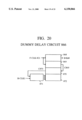
- FIG. 20 is a detailed circuit diagram of dummy delay circuit 866.
- Dummy delay circuit 866 shown in FIG. 20 generates with greater precision the time TA required for one-way propagation along the forward and backward wirings.
- Phase comparison circuit 871 inputs, as reference clock, the back clock B-CLK1 that returns along the right-hand forward and backward wirings 824, 827 of FIG. 15 and furthermore inputs clock C870 generated by forward clock F-CLK passing through the two variable-delay circuits 869, 879.
- Shift register 872 controls the delay times of variable-delay circuits 868, 869, 870 such that the phase of clock C870 coincides with the phase of back clock B-CLK1 which has a fixed delay characteristic.
- phase comparison circuit 871, shift register 872 and variable-delay circuits 868-870 have the same circuit construction as the corresponding circuits of local DLL 441.
- phase comparison circuit 871 in dummy delay circuit 866 has a slightly different construction from that of phase comparison circuit 874 in main DLL 821.
- Phase comparison circuit 874 in main DLL 821 has a construction equivalent to the phase comparison circuit shown in FIG. 8.
- the phases are deemed to be coincided when input clock in has a timing earlier than the reference clock within the delay time of delay element 500.
- phase comparison circuit 871 in dummy delay circuit 866 it is therefore desirable that the phases should be deemed to be coincided when input clock in has a timing later than the reference clock within the delay time of delay element 500.
- FIG. 21 is a timing chart of dummy delay circuit 866.
- the phase of clock C870 coincides with that of back clock B-CLK1-821, which is the reference clock. Since back clock B-CLK1-821 is delayed from forward clock F-CLK1-821 by the amount of the propagation time 2TA needed for travelling the forward and backward wirings, the delayed clock D-CLK generated by variable-delay circuit 868 is only delayed by half of clock C870 and so has a phase that is delayed from that of forward clock F-CLK-821 by propagation time TA, exactly half of the forward and backward wiring.
- main DLL 821 by controlling delayed clock D-CLK which has a phase lagging forward clock F-CLK by a time TA, such that it coincides with the phase of frequency-divided clock DIV-CLK, the forward clock F-CLK is controlled to have a phase that leads frequency-divided clock DIV-CLK by the amount of the time TA.
- FIG. 22 is a diagram showing a fourth embodiment.
- FIG. 22 parts same as in FIG. 14 are given the same reference symbols.
- the fixed delay circuit 826 which is provided in the forward and backward wiring of the right-hand-side of main DLL 821 is eliminated.
- FIG. 22 is an example of application to the case where the forward and backward wirings 824, 822, 827 on the right-hand side of main DLL 821 are considerably longer than on the left-hand side. Since the forward and backward wirings on the right-hand side already has a considerable delay time characteristic, a fixed-delay circuit is unnecessary. The delay times of the forward and backward wirings on both sides are therefore controlled to be the same by means of the variable-delay circuit 828 which is provided in the forward and backward wirings on the left-hand side of main DLL 821.
- FIG. 23 shows a fifth embodiment.
- parts same as in FIG. 14 are given the same reference symbols.
- the internal clock wiring is eliminated and the delayed forward clock F-CLK also serves the function of the internal clock of FIG. 14 without being subjected to frequency division in the local DLL group. That is, this is the same as the example shown in FIG. 1.
- a fixed-delay circuit 826 and variable-delay circuit 828 are therefore provided in the left and right forward and backward wirings as in FIG. 14, and the phases of the left-hand and right-hand back clocks are controlled to be the same.
- FIG. 24 shows a sixth embodiment.
- parts same as in FIG. 23 are given the same reference symbols.
- the fixed-delay circuit is eliminated from the right-hand forward and backward wirings. In other respects, this example is the same as FIG. 24.
- a plurality of local DLLs which are arranged on both sides of the main DLL can generate local clocks having the same phase, irrespective of the location in which the main DLL is provided and irrespective of the delay characteristics of the left-hand side and right-hand side forward and backward wirings.
Abstract
Description
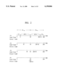
{t1+(2td-t1)}/2=td
{t2+(2td-t2)}/2=td
{t3+(2td-t3)}/2=td
{t4+(2td-t4)}/2=td
Claims (16)
Applications Claiming Priority (4)
| Application Number | Priority Date | Filing Date | Title |
|---|---|---|---|
| JP9083050A JPH10283059A (en) | 1997-04-01 | 1997-04-01 | Clock supply circuit and integrated circuit device utilizing the same |
| JP9-083050 | 1997-04-01 | ||
| JP09123897A JP3896632B2 (en) | 1997-04-10 | 1997-04-10 | Integrated circuit |
| JP9-091238 | 1997-04-10 |
Publications (1)
| Publication Number | Publication Date |
|---|---|
| US6150866A true US6150866A (en) | 2000-11-21 |
Family
ID=26424120
Family Applications (1)
| Application Number | Title | Priority Date | Filing Date |
|---|---|---|---|
| US08/977,690 Expired - Lifetime US6150866A (en) | 1997-04-01 | 1997-11-24 | Clock supplying circuit and integrated circuit device using it |
Country Status (1)
| Country | Link |
|---|---|
| US (1) | US6150866A (en) |
Cited By (51)
| Publication number | Priority date | Publication date | Assignee | Title |
|---|---|---|---|---|
| US6226757B1 (en) * | 1997-10-10 | 2001-05-01 | Rambus Inc | Apparatus and method for bus timing compensation |
| US6563358B1 (en) * | 2000-09-20 | 2003-05-13 | Nortel Networks Limited | Technique for distributing common phase clock signals |
| US20040008730A1 (en) * | 2002-07-15 | 2004-01-15 | Globespanvirata Incorporated | System and method for improved synchronous data access |
| US6680866B2 (en) | 2001-10-05 | 2004-01-20 | Renesas Technology Corp. | Clock synchronous semiconductor memory device |
| US6832347B1 (en) * | 1999-06-08 | 2004-12-14 | Cisco Technology, Inc. | Clock synchronization and fault protection for a telecommunications device |
| US20060067155A1 (en) * | 2004-09-24 | 2006-03-30 | To Hing Y | Latency normalization by balancing early and late clocks |
| US7023257B1 (en) * | 2000-10-26 | 2006-04-04 | Cypress Semiconductor Corp. | Architecture for synchronizing and resetting clock signals supplied to multiple programmable analog blocks |
| US20070002845A1 (en) * | 2005-06-14 | 2007-01-04 | International Business Machines Corporation | Multi-channel synchronization architecture |
| US20070201596A1 (en) * | 2006-02-28 | 2007-08-30 | Flowers John P | Clock synchronization using early clock |
| US7350116B1 (en) | 1999-06-08 | 2008-03-25 | Cisco Technology, Inc. | Clock synchronization and fault protection for a telecommunications device |
| US20090086867A1 (en) * | 2007-07-20 | 2009-04-02 | Mihai Banu | Method and System for Multi-Point Signal Generation with Phase Synchronized Local Carriers |
| US7737724B2 (en) | 2007-04-17 | 2010-06-15 | Cypress Semiconductor Corporation | Universal digital block interconnection and channel routing |
| US7761845B1 (en) | 2002-09-09 | 2010-07-20 | Cypress Semiconductor Corporation | Method for parameterizing a user module |
| US7765095B1 (en) | 2000-10-26 | 2010-07-27 | Cypress Semiconductor Corporation | Conditional branching in an in-circuit emulation system |
| US7770113B1 (en) | 2001-11-19 | 2010-08-03 | Cypress Semiconductor Corporation | System and method for dynamically generating a configuration datasheet |
| US7774190B1 (en) | 2001-11-19 | 2010-08-10 | Cypress Semiconductor Corporation | Sleep and stall in an in-circuit emulation system |
| US7825688B1 (en) | 2000-10-26 | 2010-11-02 | Cypress Semiconductor Corporation | Programmable microcontroller architecture(mixed analog/digital) |
| US7844437B1 (en) | 2001-11-19 | 2010-11-30 | Cypress Semiconductor Corporation | System and method for performing next placements and pruning of disallowed placements for programming an integrated circuit |
| US7893724B2 (en) | 2004-03-25 | 2011-02-22 | Cypress Semiconductor Corporation | Method and circuit for rapid alignment of signals |
| US8026739B2 (en) | 2007-04-17 | 2011-09-27 | Cypress Semiconductor Corporation | System level interconnect with programmable switching |
| US8040266B2 (en) | 2007-04-17 | 2011-10-18 | Cypress Semiconductor Corporation | Programmable sigma-delta analog-to-digital converter |
| US8049569B1 (en) | 2007-09-05 | 2011-11-01 | Cypress Semiconductor Corporation | Circuit and method for improving the accuracy of a crystal-less oscillator having dual-frequency modes |
| US8067948B2 (en) | 2006-03-27 | 2011-11-29 | Cypress Semiconductor Corporation | Input/output multiplexer bus |
| US8069436B2 (en) | 2004-08-13 | 2011-11-29 | Cypress Semiconductor Corporation | Providing hardware independence to automate code generation of processing device firmware |
| US8069428B1 (en) | 2001-10-24 | 2011-11-29 | Cypress Semiconductor Corporation | Techniques for generating microcontroller configuration information |
| US8069405B1 (en) | 2001-11-19 | 2011-11-29 | Cypress Semiconductor Corporation | User interface for efficiently browsing an electronic document using data-driven tabs |
| US8078970B1 (en) | 2001-11-09 | 2011-12-13 | Cypress Semiconductor Corporation | Graphical user interface with user-selectable list-box |
| US8078894B1 (en) | 2007-04-25 | 2011-12-13 | Cypress Semiconductor Corporation | Power management architecture, method and configuration system |
| US8085067B1 (en) | 2005-12-21 | 2011-12-27 | Cypress Semiconductor Corporation | Differential-to-single ended signal converter circuit and method |
| US8085100B2 (en) | 2005-02-04 | 2011-12-27 | Cypress Semiconductor Corporation | Poly-phase frequency synthesis oscillator |
| US8089461B2 (en) | 2005-06-23 | 2012-01-03 | Cypress Semiconductor Corporation | Touch wake for electronic devices |
| US8092083B2 (en) | 2007-04-17 | 2012-01-10 | Cypress Semiconductor Corporation | Temperature sensor with digital bandgap |
| US8103497B1 (en) | 2002-03-28 | 2012-01-24 | Cypress Semiconductor Corporation | External interface for event architecture |
| US8103496B1 (en) | 2000-10-26 | 2012-01-24 | Cypress Semicondutor Corporation | Breakpoint control in an in-circuit emulation system |
| US8120408B1 (en) | 2005-05-05 | 2012-02-21 | Cypress Semiconductor Corporation | Voltage controlled oscillator delay cell and method |
| US8130025B2 (en) | 2007-04-17 | 2012-03-06 | Cypress Semiconductor Corporation | Numerical band gap |
| US8149048B1 (en) | 2000-10-26 | 2012-04-03 | Cypress Semiconductor Corporation | Apparatus and method for programmable power management in a programmable analog circuit block |
| US8160864B1 (en) | 2000-10-26 | 2012-04-17 | Cypress Semiconductor Corporation | In-circuit emulator and pod synchronized boot |
| US8176296B2 (en) | 2000-10-26 | 2012-05-08 | Cypress Semiconductor Corporation | Programmable microcontroller architecture |
| US8286125B2 (en) | 2004-08-13 | 2012-10-09 | Cypress Semiconductor Corporation | Model for a hardware device-independent method of defining embedded firmware for programmable systems |
| US8402313B1 (en) | 2002-05-01 | 2013-03-19 | Cypress Semiconductor Corporation | Reconfigurable testing system and method |
| US8499270B1 (en) | 2007-04-25 | 2013-07-30 | Cypress Semiconductor Corporation | Configuration of programmable IC design elements |
| US8516025B2 (en) | 2007-04-17 | 2013-08-20 | Cypress Semiconductor Corporation | Clock driven dynamic datapath chaining |
| US8527949B1 (en) | 2001-11-19 | 2013-09-03 | Cypress Semiconductor Corporation | Graphical user interface for dynamically reconfiguring a programmable device |
| US8745561B1 (en) * | 2013-03-15 | 2014-06-03 | Cadence Design Systems, Inc. | System and method for common path pessimism reduction in timing analysis to guide remedial transformations of a circuit design |
| US20150067383A1 (en) * | 2013-08-30 | 2015-03-05 | Cavium, Inc. | Distributed Delay Locked Loop |
| US20150381189A1 (en) * | 2009-08-27 | 2015-12-31 | Micron Technology, Inc. | Die location compensation |
| US9448964B2 (en) | 2009-05-04 | 2016-09-20 | Cypress Semiconductor Corporation | Autonomous control in a programmable system |
| US9564902B2 (en) | 2007-04-17 | 2017-02-07 | Cypress Semiconductor Corporation | Dynamically configurable and re-configurable data path |
| US9720805B1 (en) | 2007-04-25 | 2017-08-01 | Cypress Semiconductor Corporation | System and method for controlling a target device |
| US10698662B2 (en) | 2001-11-15 | 2020-06-30 | Cypress Semiconductor Corporation | System providing automatic source code generation for personalization and parameterization of user modules |
Citations (3)
| Publication number | Priority date | Publication date | Assignee | Title |
|---|---|---|---|---|
| US5696951A (en) * | 1996-01-03 | 1997-12-09 | Credence Systems Corporation | Signal deskewing system for synchronous logic circuit |
| US5712882A (en) * | 1996-01-03 | 1998-01-27 | Credence Systems Corporation | Signal distribution system |
| US5734685A (en) * | 1996-01-03 | 1998-03-31 | Credence Systems Corporation | Clock signal deskewing system |
-
1997
- 1997-11-24 US US08/977,690 patent/US6150866A/en not_active Expired - Lifetime
Patent Citations (3)
| Publication number | Priority date | Publication date | Assignee | Title |
|---|---|---|---|---|
| US5696951A (en) * | 1996-01-03 | 1997-12-09 | Credence Systems Corporation | Signal deskewing system for synchronous logic circuit |
| US5712882A (en) * | 1996-01-03 | 1998-01-27 | Credence Systems Corporation | Signal distribution system |
| US5734685A (en) * | 1996-01-03 | 1998-03-31 | Credence Systems Corporation | Clock signal deskewing system |
Cited By (77)
| Publication number | Priority date | Publication date | Assignee | Title |
|---|---|---|---|---|
| US6226757B1 (en) * | 1997-10-10 | 2001-05-01 | Rambus Inc | Apparatus and method for bus timing compensation |
| US6832347B1 (en) * | 1999-06-08 | 2004-12-14 | Cisco Technology, Inc. | Clock synchronization and fault protection for a telecommunications device |
| US7350116B1 (en) | 1999-06-08 | 2008-03-25 | Cisco Technology, Inc. | Clock synchronization and fault protection for a telecommunications device |
| US6563358B1 (en) * | 2000-09-20 | 2003-05-13 | Nortel Networks Limited | Technique for distributing common phase clock signals |
| US8555032B2 (en) | 2000-10-26 | 2013-10-08 | Cypress Semiconductor Corporation | Microcontroller programmable system on a chip with programmable interconnect |
| US10248604B2 (en) | 2000-10-26 | 2019-04-02 | Cypress Semiconductor Corporation | Microcontroller programmable system on a chip |
| US8103496B1 (en) | 2000-10-26 | 2012-01-24 | Cypress Semicondutor Corporation | Breakpoint control in an in-circuit emulation system |
| US7023257B1 (en) * | 2000-10-26 | 2006-04-04 | Cypress Semiconductor Corp. | Architecture for synchronizing and resetting clock signals supplied to multiple programmable analog blocks |
| US10725954B2 (en) | 2000-10-26 | 2020-07-28 | Monterey Research, Llc | Microcontroller programmable system on a chip |
| US8149048B1 (en) | 2000-10-26 | 2012-04-03 | Cypress Semiconductor Corporation | Apparatus and method for programmable power management in a programmable analog circuit block |
| US8176296B2 (en) | 2000-10-26 | 2012-05-08 | Cypress Semiconductor Corporation | Programmable microcontroller architecture |
| US9766650B2 (en) | 2000-10-26 | 2017-09-19 | Cypress Semiconductor Corporation | Microcontroller programmable system on a chip with programmable interconnect |
| US9843327B1 (en) | 2000-10-26 | 2017-12-12 | Cypress Semiconductor Corporation | PSOC architecture |
| US10020810B2 (en) | 2000-10-26 | 2018-07-10 | Cypress Semiconductor Corporation | PSoC architecture |
| US10261932B2 (en) | 2000-10-26 | 2019-04-16 | Cypress Semiconductor Corporation | Microcontroller programmable system on a chip |
| US8358150B1 (en) | 2000-10-26 | 2013-01-22 | Cypress Semiconductor Corporation | Programmable microcontroller architecture(mixed analog/digital) |
| US8736303B2 (en) | 2000-10-26 | 2014-05-27 | Cypress Semiconductor Corporation | PSOC architecture |
| US7765095B1 (en) | 2000-10-26 | 2010-07-27 | Cypress Semiconductor Corporation | Conditional branching in an in-circuit emulation system |
| US8160864B1 (en) | 2000-10-26 | 2012-04-17 | Cypress Semiconductor Corporation | In-circuit emulator and pod synchronized boot |
| US7825688B1 (en) | 2000-10-26 | 2010-11-02 | Cypress Semiconductor Corporation | Programmable microcontroller architecture(mixed analog/digital) |
| KR100491459B1 (en) * | 2001-10-05 | 2005-05-25 | 미쓰비시덴키 가부시키가이샤 | Semiconductor memory device |
| US6680866B2 (en) | 2001-10-05 | 2004-01-20 | Renesas Technology Corp. | Clock synchronous semiconductor memory device |
| US8069428B1 (en) | 2001-10-24 | 2011-11-29 | Cypress Semiconductor Corporation | Techniques for generating microcontroller configuration information |
| US10466980B2 (en) | 2001-10-24 | 2019-11-05 | Cypress Semiconductor Corporation | Techniques for generating microcontroller configuration information |
| US8793635B1 (en) | 2001-10-24 | 2014-07-29 | Cypress Semiconductor Corporation | Techniques for generating microcontroller configuration information |
| US8078970B1 (en) | 2001-11-09 | 2011-12-13 | Cypress Semiconductor Corporation | Graphical user interface with user-selectable list-box |
| US10698662B2 (en) | 2001-11-15 | 2020-06-30 | Cypress Semiconductor Corporation | System providing automatic source code generation for personalization and parameterization of user modules |
| US7844437B1 (en) | 2001-11-19 | 2010-11-30 | Cypress Semiconductor Corporation | System and method for performing next placements and pruning of disallowed placements for programming an integrated circuit |
| US7774190B1 (en) | 2001-11-19 | 2010-08-10 | Cypress Semiconductor Corporation | Sleep and stall in an in-circuit emulation system |
| US8069405B1 (en) | 2001-11-19 | 2011-11-29 | Cypress Semiconductor Corporation | User interface for efficiently browsing an electronic document using data-driven tabs |
| US7770113B1 (en) | 2001-11-19 | 2010-08-03 | Cypress Semiconductor Corporation | System and method for dynamically generating a configuration datasheet |
| US8533677B1 (en) | 2001-11-19 | 2013-09-10 | Cypress Semiconductor Corporation | Graphical user interface for dynamically reconfiguring a programmable device |
| US8527949B1 (en) | 2001-11-19 | 2013-09-03 | Cypress Semiconductor Corporation | Graphical user interface for dynamically reconfiguring a programmable device |
| US8370791B2 (en) | 2001-11-19 | 2013-02-05 | Cypress Semiconductor Corporation | System and method for performing next placements and pruning of disallowed placements for programming an integrated circuit |
| US8103497B1 (en) | 2002-03-28 | 2012-01-24 | Cypress Semiconductor Corporation | External interface for event architecture |
| US8402313B1 (en) | 2002-05-01 | 2013-03-19 | Cypress Semiconductor Corporation | Reconfigurable testing system and method |
| US7418616B2 (en) | 2002-07-15 | 2008-08-26 | Brooktree Broadband Holding, Inc. | System and method for improved synchronous data access |
| US20040008730A1 (en) * | 2002-07-15 | 2004-01-15 | Globespanvirata Incorporated | System and method for improved synchronous data access |
| US7761845B1 (en) | 2002-09-09 | 2010-07-20 | Cypress Semiconductor Corporation | Method for parameterizing a user module |
| US7893724B2 (en) | 2004-03-25 | 2011-02-22 | Cypress Semiconductor Corporation | Method and circuit for rapid alignment of signals |
| US8069436B2 (en) | 2004-08-13 | 2011-11-29 | Cypress Semiconductor Corporation | Providing hardware independence to automate code generation of processing device firmware |
| US8286125B2 (en) | 2004-08-13 | 2012-10-09 | Cypress Semiconductor Corporation | Model for a hardware device-independent method of defining embedded firmware for programmable systems |
| US7324403B2 (en) * | 2004-09-24 | 2008-01-29 | Intel Corporation | Latency normalization by balancing early and late clocks |
| US20060067155A1 (en) * | 2004-09-24 | 2006-03-30 | To Hing Y | Latency normalization by balancing early and late clocks |
| US8085100B2 (en) | 2005-02-04 | 2011-12-27 | Cypress Semiconductor Corporation | Poly-phase frequency synthesis oscillator |
| US8120408B1 (en) | 2005-05-05 | 2012-02-21 | Cypress Semiconductor Corporation | Voltage controlled oscillator delay cell and method |
| US7512201B2 (en) * | 2005-06-14 | 2009-03-31 | International Business Machines Corporation | Multi-channel synchronization architecture |
| US20070002845A1 (en) * | 2005-06-14 | 2007-01-04 | International Business Machines Corporation | Multi-channel synchronization architecture |
| US8089461B2 (en) | 2005-06-23 | 2012-01-03 | Cypress Semiconductor Corporation | Touch wake for electronic devices |
| US8085067B1 (en) | 2005-12-21 | 2011-12-27 | Cypress Semiconductor Corporation | Differential-to-single ended signal converter circuit and method |
| US20070201596A1 (en) * | 2006-02-28 | 2007-08-30 | Flowers John P | Clock synchronization using early clock |
| US8067948B2 (en) | 2006-03-27 | 2011-11-29 | Cypress Semiconductor Corporation | Input/output multiplexer bus |
| US8717042B1 (en) | 2006-03-27 | 2014-05-06 | Cypress Semiconductor Corporation | Input/output multiplexer bus |
| US8476928B1 (en) | 2007-04-17 | 2013-07-02 | Cypress Semiconductor Corporation | System level interconnect with programmable switching |
| US8516025B2 (en) | 2007-04-17 | 2013-08-20 | Cypress Semiconductor Corporation | Clock driven dynamic datapath chaining |
| US9564902B2 (en) | 2007-04-17 | 2017-02-07 | Cypress Semiconductor Corporation | Dynamically configurable and re-configurable data path |
| US8026739B2 (en) | 2007-04-17 | 2011-09-27 | Cypress Semiconductor Corporation | System level interconnect with programmable switching |
| US8130025B2 (en) | 2007-04-17 | 2012-03-06 | Cypress Semiconductor Corporation | Numerical band gap |
| US8092083B2 (en) | 2007-04-17 | 2012-01-10 | Cypress Semiconductor Corporation | Temperature sensor with digital bandgap |
| US7737724B2 (en) | 2007-04-17 | 2010-06-15 | Cypress Semiconductor Corporation | Universal digital block interconnection and channel routing |
| US8040266B2 (en) | 2007-04-17 | 2011-10-18 | Cypress Semiconductor Corporation | Programmable sigma-delta analog-to-digital converter |
| US8909960B1 (en) | 2007-04-25 | 2014-12-09 | Cypress Semiconductor Corporation | Power management architecture, method and configuration system |
| US8078894B1 (en) | 2007-04-25 | 2011-12-13 | Cypress Semiconductor Corporation | Power management architecture, method and configuration system |
| US9720805B1 (en) | 2007-04-25 | 2017-08-01 | Cypress Semiconductor Corporation | System and method for controlling a target device |
| US8499270B1 (en) | 2007-04-25 | 2013-07-30 | Cypress Semiconductor Corporation | Configuration of programmable IC design elements |
| US8873690B2 (en) | 2007-07-20 | 2014-10-28 | Blue Danube Labs, Inc. | Method and system for multi-point signal generation with phase synchronized local carriers |
| US20090086867A1 (en) * | 2007-07-20 | 2009-04-02 | Mihai Banu | Method and System for Multi-Point Signal Generation with Phase Synchronized Local Carriers |
| US8259884B2 (en) | 2007-07-20 | 2012-09-04 | Blue Danube Labs, Inc. | Method and system for multi-point signal generation with phase synchronized local carriers |
| US8049569B1 (en) | 2007-09-05 | 2011-11-01 | Cypress Semiconductor Corporation | Circuit and method for improving the accuracy of a crystal-less oscillator having dual-frequency modes |
| US9448964B2 (en) | 2009-05-04 | 2016-09-20 | Cypress Semiconductor Corporation | Autonomous control in a programmable system |
| US10063241B2 (en) * | 2009-08-27 | 2018-08-28 | Micron Technology, Inc. | Die location compensation |
| US20150381189A1 (en) * | 2009-08-27 | 2015-12-31 | Micron Technology, Inc. | Die location compensation |
| US8745561B1 (en) * | 2013-03-15 | 2014-06-03 | Cadence Design Systems, Inc. | System and method for common path pessimism reduction in timing analysis to guide remedial transformations of a circuit design |
| CN104426539B (en) * | 2013-08-30 | 2018-01-23 | 凯为公司 | Distributed delay locked loop |
| US9335784B2 (en) * | 2013-08-30 | 2016-05-10 | Cavium, Inc. | Clock distribution circuit with distributed delay locked loop |
| CN104426539A (en) * | 2013-08-30 | 2015-03-18 | 凯为公司 | Distributed delay locked loop |
| US20150067383A1 (en) * | 2013-08-30 | 2015-03-05 | Cavium, Inc. | Distributed Delay Locked Loop |
Similar Documents
| Publication | Publication Date | Title |
|---|---|---|
| US6150866A (en) | Clock supplying circuit and integrated circuit device using it | |
| US6445231B1 (en) | Digital dual-loop DLL design using coarse and fine loops | |
| US5939913A (en) | DLL circuit and semiconductor memory device using same | |
| US5973525A (en) | Integrated circuit device | |
| KR100631164B1 (en) | Register controlled delay locked loop with low power consumption | |
| JP3644827B2 (en) | DLL circuit considering external load | |
| JP3085258B2 (en) | Clock signal distribution circuit | |
| KR100527402B1 (en) | Delay locked loop of DDR SDRAM | |
| KR100256004B1 (en) | Semiconductor memory system using a clock-synchronous semiconductor device, and an semiconductor memory device for use in the same | |
| US5712884A (en) | Data receiving method and circuit of digital communication system | |
| JP4817348B2 (en) | Delay locked loop used in semiconductor memory device | |
| US6194932B1 (en) | Integrated circuit device | |
| JP4480471B2 (en) | Register controlled delay lock loop | |
| JP3481148B2 (en) | Integrated circuit device having DLL circuit | |
| KR19990066735A (en) | Semiconductor devices | |
| US6064244A (en) | Phase-locked loop circuit permitting reduction of circuit size | |
| KR20200038555A (en) | Devices and methods for detecting loop count in delay-fixed loop | |
| JP3497710B2 (en) | Semiconductor device | |
| KR19980041728A (en) | Semiconductor integrated circuit | |
| KR100299357B1 (en) | Delay locked loop circuit for controlling delay time with reduced lock-up time | |
| US6225843B1 (en) | Semiconductor integrated circuit device | |
| CN100440371C (en) | Delay locked loop (dll) circuit and method for locking clock delay by using the same | |
| US6608514B1 (en) | Clock signal generator circuit and semiconductor integrated circuit with the same circuit | |
| KR100276572B1 (en) | Integrated circuit device | |
| KR100300244B1 (en) | Clock supplying circuit and integrated circuit device using it |
Legal Events
| Date | Code | Title | Description |
|---|---|---|---|
| AS | Assignment |
Owner name: FUJITSU LIMITED, JAPAN Free format text: ASSIGNMENT OF ASSIGNORS INTEREST;ASSIGNORS:ETO, SATOSHI;NAKAMURA, TOSHIKAZU;REEL/FRAME:008903/0901 Effective date: 19971101 |
|
| STCF | Information on status: patent grant |
Free format text: PATENTED CASE |
|
| FEPP | Fee payment procedure |
Free format text: PAYOR NUMBER ASSIGNED (ORIGINAL EVENT CODE: ASPN); ENTITY STATUS OF PATENT OWNER: LARGE ENTITY |
|
| FPAY | Fee payment |
Year of fee payment: 4 |
|
| FPAY | Fee payment |
Year of fee payment: 8 |
|
| AS | Assignment |
Owner name: FUJITSU MICROELECTRONICS LIMITED, JAPAN Free format text: ASSIGNMENT OF ASSIGNORS INTEREST;ASSIGNOR:FUJITSU LIMITED;REEL/FRAME:021998/0645 Effective date: 20081104 Owner name: FUJITSU MICROELECTRONICS LIMITED,JAPAN Free format text: ASSIGNMENT OF ASSIGNORS INTEREST;ASSIGNOR:FUJITSU LIMITED;REEL/FRAME:021998/0645 Effective date: 20081104 |
|
| AS | Assignment |
Owner name: FUJITSU SEMICONDUCTOR LIMITED, JAPAN Free format text: CHANGE OF NAME;ASSIGNOR:FUJITSU MICROELECTRONICS LIMITED;REEL/FRAME:024982/0245 Effective date: 20100401 |
|
| FPAY | Fee payment |
Year of fee payment: 12 |
|
| AS | Assignment |
Owner name: SOCIONEXT INC., JAPAN Free format text: ASSIGNMENT OF ASSIGNORS INTEREST;ASSIGNOR:FUJITSU SEMICONDUCTOR LIMITED;REEL/FRAME:035508/0637 Effective date: 20150302 |