US6150890A - Dual band transmitter for a cellular phone comprising a PLL - Google Patents
Dual band transmitter for a cellular phone comprising a PLL Download PDFInfo
- Publication number
- US6150890A US6150890A US09/163,798 US16379898A US6150890A US 6150890 A US6150890 A US 6150890A US 16379898 A US16379898 A US 16379898A US 6150890 A US6150890 A US 6150890A
- Authority
- US
- United States
- Prior art keywords
- output
- frequency
- vco
- phase detector
- value
- Prior art date
- Legal status (The legal status is an assumption and is not a legal conclusion. Google has not performed a legal analysis and makes no representation as to the accuracy of the status listed.)
- Expired - Lifetime
Links
Images
Classifications
-
- H—ELECTRICITY
- H04—ELECTRIC COMMUNICATION TECHNIQUE
- H04B—TRANSMISSION
- H04B1/00—Details of transmission systems, not covered by a single one of groups H04B3/00 - H04B13/00; Details of transmission systems not characterised by the medium used for transmission
- H04B1/005—Details of transmission systems, not covered by a single one of groups H04B3/00 - H04B13/00; Details of transmission systems not characterised by the medium used for transmission adapting radio receivers, transmitters andtransceivers for operation on two or more bands, i.e. frequency ranges
-
- H—ELECTRICITY
- H03—ELECTRONIC CIRCUITRY
- H03J—TUNING RESONANT CIRCUITS; SELECTING RESONANT CIRCUITS
- H03J5/00—Discontinuous tuning; Selecting predetermined frequencies; Selecting frequency bands with or without continuous tuning in one or more of the bands, e.g. push-button tuning, turret tuner
- H03J5/24—Discontinuous tuning; Selecting predetermined frequencies; Selecting frequency bands with or without continuous tuning in one or more of the bands, e.g. push-button tuning, turret tuner with a number of separate pretuned tuning circuits or separate tuning elements selectively brought into circuit, e.g. for waveband selection or for television channel selection
- H03J5/242—Discontinuous tuning; Selecting predetermined frequencies; Selecting frequency bands with or without continuous tuning in one or more of the bands, e.g. push-button tuning, turret tuner with a number of separate pretuned tuning circuits or separate tuning elements selectively brought into circuit, e.g. for waveband selection or for television channel selection used exclusively for band selection
- H03J5/244—Discontinuous tuning; Selecting predetermined frequencies; Selecting frequency bands with or without continuous tuning in one or more of the bands, e.g. push-button tuning, turret tuner with a number of separate pretuned tuning circuits or separate tuning elements selectively brought into circuit, e.g. for waveband selection or for television channel selection used exclusively for band selection using electronic means
-
- H—ELECTRICITY
- H03—ELECTRONIC CIRCUITRY
- H03L—AUTOMATIC CONTROL, STARTING, SYNCHRONISATION, OR STABILISATION OF GENERATORS OF ELECTRONIC OSCILLATIONS OR PULSES
- H03L7/00—Automatic control of frequency or phase; Synchronisation
- H03L7/06—Automatic control of frequency or phase; Synchronisation using a reference signal applied to a frequency- or phase-locked loop
- H03L7/08—Details of the phase-locked loop
- H03L7/085—Details of the phase-locked loop concerning mainly the frequency- or phase-detection arrangement including the filtering or amplification of its output signal
- H03L7/093—Details of the phase-locked loop concerning mainly the frequency- or phase-detection arrangement including the filtering or amplification of its output signal using special filtering or amplification characteristics in the loop
-
- H—ELECTRICITY
- H03—ELECTRONIC CIRCUITRY
- H03L—AUTOMATIC CONTROL, STARTING, SYNCHRONISATION, OR STABILISATION OF GENERATORS OF ELECTRONIC OSCILLATIONS OR PULSES
- H03L7/00—Automatic control of frequency or phase; Synchronisation
- H03L7/06—Automatic control of frequency or phase; Synchronisation using a reference signal applied to a frequency- or phase-locked loop
- H03L7/16—Indirect frequency synthesis, i.e. generating a desired one of a number of predetermined frequencies using a frequency- or phase-locked loop
- H03L7/18—Indirect frequency synthesis, i.e. generating a desired one of a number of predetermined frequencies using a frequency- or phase-locked loop using a frequency divider or counter in the loop
- H03L7/183—Indirect frequency synthesis, i.e. generating a desired one of a number of predetermined frequencies using a frequency- or phase-locked loop using a frequency divider or counter in the loop a time difference being used for locking the loop, the counter counting between fixed numbers or the frequency divider dividing by a fixed number
- H03L7/185—Indirect frequency synthesis, i.e. generating a desired one of a number of predetermined frequencies using a frequency- or phase-locked loop using a frequency divider or counter in the loop a time difference being used for locking the loop, the counter counting between fixed numbers or the frequency divider dividing by a fixed number using a mixer in the loop
-
- H—ELECTRICITY
- H04—ELECTRIC COMMUNICATION TECHNIQUE
- H04B—TRANSMISSION
- H04B1/00—Details of transmission systems, not covered by a single one of groups H04B3/00 - H04B13/00; Details of transmission systems not characterised by the medium used for transmission
- H04B1/38—Transceivers, i.e. devices in which transmitter and receiver form a structural unit and in which at least one part is used for functions of transmitting and receiving
- H04B1/40—Circuits
- H04B1/403—Circuits using the same oscillator for generating both the transmitter frequency and the receiver local oscillator frequency
- H04B1/406—Circuits using the same oscillator for generating both the transmitter frequency and the receiver local oscillator frequency with more than one transmission mode, e.g. analog and digital modes
-
- H—ELECTRICITY
- H03—ELECTRONIC CIRCUITRY
- H03L—AUTOMATIC CONTROL, STARTING, SYNCHRONISATION, OR STABILISATION OF GENERATORS OF ELECTRONIC OSCILLATIONS OR PULSES
- H03L2207/00—Indexing scheme relating to automatic control of frequency or phase and to synchronisation
- H03L2207/10—Indirect frequency synthesis using a frequency multiplier in the phase-locked loop or in the reference signal path
Definitions
- the invention relates to transmitters used in a communications system. More particularly, the invention relates to a phase-locked loop (PLL) of a dual band transmitter used in a wireless phone, such as a dual band cellular phone for mobile communications systems.
- PLL phase-locked loop
- GSM Global System for Mobile communications
- ETSI European Telecommunications Standards Institute
- GSM Global System for Mobile communications
- DCS1800 Digital Communications System
- Other environments include systems known as Advanced Mobile Phone System (AMPS) operating in a frequency band around 800 MHz, and as Personal Communications System (PCS) operating in a frequency band around 1900 MHz.
- AMPS Advanced Mobile Phone System
- PCS Personal Communications System
- a cellular phone operable at two frequency bands is referred to as a dual band cellular phone.
- the dual band cellular phone has to transmit signals at both frequency bands, duplication of functions is required.
- a second PLL is required in a GSM900/DCS1800 dual band cellular telephone having transmit frequency bands between 890 MHz and 915 MHz for the GSM band, and between 1710 MHz and 1785 MHz for the DCS 1800 band.
- VCO voltage-controlled oscillators
- Duplication of functions such as VCOs leads to higher manufacturing costs and ultimately to higher prices for the dual band cellular phones.
- An aspect of the invention involves a cellular phone for a mobile communications system.
- the phone is operable in a first radio frequency band and a second radio frequency band and comprises a dual band transmitter and an antenna.
- the dual band transmitter comprises a phase-locked loop (PLL) which can generate two or more output frequency ranges.
- the PLL comprises a first frequency divider configured to divide a frequency signal by a value N, a phase detector responsive to an output of the first divider, and a loop filter responsive to an output of the phase detector.
- a voltage-controlled oscillator (VCO) is responsive to an output of the loop filter and a frequency multiplier is responsive to an output of the VCO.
- VCO voltage-controlled oscillator
- a band-switch has a first input responsive to the output of the VCO, a second input responsive to an output of the frequency multiplier, and a third input responsive to a control signal to select for output from said band-switch one of the first and second inputs.
- a mixer has two inputs, one mixer input is responsive to the output of the band-switch and a second mixer input is responsive to a radio frequency signal.
- a second frequency divider is configured to divide an input frequency by a value M. The second divider is responsive to an output of the mixer, and an output of the second frequency divider provides an input to the phase detector.
- the PLL includes a phase detector, a loop filter, and a single voltage-controlled oscillator (VCO).
- VCO voltage-controlled oscillator
- An output of the VCO is multiplied by a predetermined value to produce a multiplied output, and a desired output frequency is selected. Either the output of the VCO or the multiplied output are selectively fed back to the phase detector, based upon the selected desired output frequency.
- the output of the VCO is selected, the output of the VCO is fed back, and when the multiplied output is selected, the multiplied output is fed back.
- a further aspect of the invention involves a dual band transmitter for a wireless phone.
- the dual band transmitter comprises a first power amplifier, a second power amplifier and a phase locked loop (PLL).
- the first power amplifier has a first input for a first signal in a first radio frequency band, and a first output for an amplified first signal.
- the first output is connectable to an antenna.
- the second power amplifier has a second input for a second signal in a second radio frequency band and a second output for an amplified second signal.
- the second output is connectable to the antenna.
- the PLL can generate two or more output frequency ranges and comprises a first frequency divider configured to divide a frequency signal by a value N.
- a phase detector is responsive to an output of the first divider and a loop filter is responsive to an output of the phase detector.
- a voltage-controlled oscillator (VCO) is responsive to an output of the loop filter and a frequency multiplier is responsive to an output of the VCO.
- a band-switch has a first input responsive to the output of the VCO, a second input responsive to an output of the frequency multiplier, and a third input responsive to a control signal to select for output from the band-switch one of the first and second inputs.
- a mixer has two inputs, one mixer input is responsive to the output of the band-switch and a second mixer input is responsive to a radio frequency signal.
- a second frequency divider is configured to divide an input frequency by a value M. The second divider is responsive to an output of the mixer, and an output of the second frequency divider provides an input to the phase detector.
- a further aspect of the invention involves a dual band transmitter for a wireless phone.
- the dual band transmitter comprises a first power amplifier, a second power amplifier and a phase locked loop (PLL).
- the first power amplifier has a first input for a first signal in a first radio frequency band, and a first output for an amplified first signal.
- the first output is connectable to an antenna.
- the second power amplifier has a second input for a second signal in a second radio frequency band and a second output for an amplified second signal.
- the second output is connectable to the antenna.
- the PLL can generate two or more output frequency ranges.
- the PLL comprises a first frequency divider configured to divide a frequency signal by a value N, a phase detector responsive to an output of the first frequency divider and a loop filter responsive to an output of the phase detector.
- a voltage-controlled oscillator (VCO) is responsive to an output of the loop filter, and at least one frequency multiplier is responsive to an output of the VCO.
- VCO voltage-controlled oscillator
- a mixer has two inputs, one mixer input is responsive to the output of the VCO and a second mixer input is responsive to a local oscillator signal.
- the second frequency divider is configured to divide an input frequency by a value M and connected to an output of the mixer.
- An output of the second divider provides an input to the phase detector, and a selector is connected to the output of the at least one frequency multiplier. The selector is configured to select an output frequency.
- the phone is operable in a first radio frequency band and a second radio frequency band, and comprises a dual band transmitter and an antenna.
- the dual band transmitter comprises a phase-locked loop (PLL) which can generate two or more output frequency ranges.
- the PLL comprises a first frequency divider configured to divide a frequency signal by a value N, and a phase detector responsive to an output of the first frequency divider.
- a loop filter is responsive to an output of the phase detector and a voltage-controlled oscillator (VCO) is responsive to an output of the loop filter.
- At least one frequency multiplier is responsive to an output of the VCO.
- a mixer has two inputs, one mixer input is responsive to the output of the VCO and a second mixer input is responsive to a local oscillator signal.
- a second frequency divider is configured to divide an input frequency by a value M and is connected to an output of the mixer.
- a output of the second divider provides an input to the phase detector.
- a selector is connected to the output of the at least one frequency multiplier and is configured to select an output frequency.
- a further aspect of the invention involves a method for generating at least two output frequency ranges from a phase locked loop (PLL) in a cellular phone for a mobile communications system.
- the PLL comprises a single voltage controlled oscillator (VCO), an adjustable first frequency divider which divides by a value N, a second frequency divider which divides by a value M, a phase detector, and a loop filter.
- VCO voltage controlled oscillator
- the method comprises multiplying an output of the VCO by a predetermined value to produce a multiplied output frequency, selecting a desired output frequency of one of the VCO output and the multiplied output frequency, and adjusting the values of the first frequency divider such that a ratio N/M equals the value of the predetermined value when the multiplied output is selected, and adjusting the ratio N/M equal to the value "1"when the VCO output is selected.
- the dual band transmitter comprises a first power amplifier, a second power amplifier, and a phase locked loop (PLL).
- the first power amplifier has a first input for a first signal in a first radio frequency band, and a first output for an amplified first signal. The first output is connectable to an antenna.
- the second power amplifier has a second input for a second signal in a second radio frequency band and a second output for an amplified second signal. The second output is connectable to the antenna.
- the PLL can generate two or more output frequency ranges.
- the PLL comprises a voltage-controlled oscillator (VCO) having a first output connected to said first power amplifier.
- the VCO generates the first signal.
- a frequency multiplier has an input connected to the first output of the VCO and a second output connected to the second power amplifier. The frequency multiplier receives the first signal and generates the second signal.
- VCO voltage-controlled oscillator
- a further aspect of the involves a method for generating two output frequency ranges from a phase locked loop (PLL) in a dual band transmitter for a wireless phone.
- the PLL comprises a single voltage controlled oscillator (VCO).
- the method comprises multiplying an output of the VCO by a predetermined value to produce a multiplied output frequency, and selecting a desired output frequency of one of the VCO output and the multiplied output frequency.
- the phone is operable in a first radio frequency band and a second radio frequency band, and comprises a dual band transmitter and an antenna.
- the dual band transmitter includes a phase-locked loop (PLL) which can generate two or more output frequency ranges.
- the PLL comprises a voltage-controlled oscillator (VCO) which has a first output connected to the first power amplifier and which generates the first signal.
- VCO voltage-controlled oscillator
- a frequency multiplier has an input connected to said first output of the VCO and a second output connected to said second power amplifier. The frequency multiplier receives the first signal and generates the second signal.
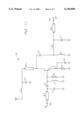
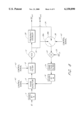
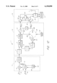
- FIG. 1 is a schematic illustration of a cellular phone cut away to show a portion of the motherboard.
- FIG. 2 is a simplified illustration of a transmit path of the cellular phone shown in FIG. 1.
- FIG. 3 is a block diagram showing a basic Phase-Locked Loop (PLL).
- PLL Phase-Locked Loop
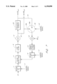
- FIG. 4 is a block diagram of a PLL frequency synthesizer utilizing a program counter in the feedback loop.
- FIG. 5 is a block diagram of a PLL wherein the feedback loop contains a mixer.
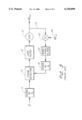
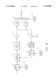
- FIG. 6 is a block diagram of a PLL according to a first embodiment of the present invention, wherein a frequency doubler and a band-switch are used to provide two different output frequency ranges.
- FIG. 7 is a block diagram of a PLL according to a second embodiment of the present invention.
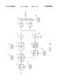
- FIG. 8 is a block diagram of a PLL according to a third embodiment of the present invention, wherein multiplier blocks and a selector are incorporated outside of the feedback loop;
- FIG. 9 is a block diagram of a PLL according to a fourth embodiment of the present invention.
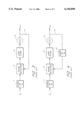
- FIG. 10 is a simplified block diagram of a dual band transmitter.
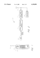
- FIG. 11 is a schematic diagram of a frequency doubler circuit.
- a preferred embodiment of the invention is described with reference to a cellular phone for use in a mobile communications system. It is contemplated that the invention is equally applicable in other wireless devices such as conventional cordless phones for home or office use.
- a mobile communications system for example according to the GSM standard, is structured to have a variety of individual regions called cells, and to comprise a variety of fixed transceiver stations called base transceiver stations, and a plurality of mobile stations, the cellular phones.
- base transceiver stations a variety of fixed transceiver stations
- mobile stations the cellular phones.
- one base transceiver station defines one cell and handles telephone traffic to and from cellular phones which are currently located in the cell.
- FIG. 1 schematically illustrates a dual band cellular phone 3 made in accordance with the invention.
- a portion of the case of the dual band cellular phone 3 is cut away to show a motherboard 5 of the cellular phone 3 with a dual band transmitter 1 positioned thereon.
- the cellular phone 3 comprises a plurality of other components and functional modules, such as the components of a receive path and a transmit path.
- the cellular phone 3 further includes an antenna 11, a display and a keypad.
- the receive path of such a dual band cellular phone 3 includes a radio frequency (RF) receiver, an analog-to-digital converter, a demultiplexer and a demodulator.
- the transmit path comprises a multiplexer, modulator, digital-to-analog converter and an RF transmitter.
- Further functional modules include, for example, a channel coder/decoder and a speech coder/decoder.
- Both the RF receiver and the RF transmitter are usually connected to the antenna 11 by means of a diode switch (eventually in combination with a band selector) which connects the antenna 11 either to the RF receiver or to the RF transmitter.
- the RF transmitter comprises an amplifier stage for amplifying the RF signals according to electrical characteristics, for example, a defined power level versus time profile and a defined spectral mask, before the RF signals are fed to the antenna 2 and emitted as radio signals.
- the spectral mask and the power level versus time profile are defined in GSM Technical Specification GSM 05.05, July 1996, Version 5.2.0, entitled "Digital cellular telecommunications system (Phase 2+); Radio transmission and reception", Paragraph 4.2.2, and Annex B.
- FIG. 2 illustrates a simplified embodiment of the transmit path of the dual band cellular phone 3.
- the receive path is indicated by means of a receiver la which includes, for example, the radio frequency (RF) receiver.
- the transmitter 1, which includes two power amplifiers, and a processing module 7 are positioned on the motherboard and interconnected between the antenna 2 and a microphone 9 of the cellular phone 3.
- the processing module 7 performs most speech and signal processing in a transmit direction, for example, voice encoding and channel encoding.
- the dual band transmitter 1 transforms the encoded signals into the RF domain. It is contemplated that the illustrated separation into a signal processing module 7 and a dual band transmitter 1 is for illustrative purposes only.
- a dual band transmitter only includes power amplifiers and any modulation is performed, for example, in the signal processing module 7.
- the dual band transmitter 1 performs all RF processing.
- the dual band transmitter modulates an RF carrier of, for example, nominal either 900 MHz or 1800 MHz with the processed speech signal.
- the RF signals emitted from the dual band transmitter 1 have frequencies within a transmit band of 890 MHz to 915 MHz for GSM900, and 1710 MHz to 1785 MHz for DCS1800.
- the dual band transmitter 1 includes a phase-locked loop (PLL) which determines the transmit bands and provides for frequency stability and accuracy.
- PLL phase-locked loop
- FIG. 3 illustrates a standard Phase-Locked Loop (PLL).
- the basic PLL has an input signal having an input frequency f in which is divided by a divider 4, wherein the divider 4 divides the input frequency f in by a value N.
- the output of the divider 4 is then input into a phase detector 6.
- the phase detector 6 outputs a voltage that is proportional to a phase difference between two input signals (frequencies).
- This phase detector output voltage is then input into a loop filter 8.
- the loop filter 8 smoothes the phase detector output voltage and determines the loop performance based upon selected loop filter values.
- the output of the loop filter 8 adjusts a voltage-controlled oscillator (VCO) 10 and determines the output frequency of the VCO 10.
- the output of the VCO 10 is then fed back as an input to the phase detector 6 via a feedback loop 14.
- the output voltage of the phase detector 6 will vary according to any change in the phase difference between the output frequency of the VCO 10 and the input frequency f
- the feedback loop 14 thus provides a means of "locking" the phase of an output frequency f out in accordance with the phase of the input frequency f in . If the input frequency f in is a highly stable reference frequency, the PLL produces a highly stable output frequency f out .
- the PLL produces an output frequency f out , equal to the value [f in /N], wherein the phase of the VCO output frequency f out , follows the phase of the input frequency f in .
- a divider 16 may be used in the feedback loop 14 in order to change the output frequency f out .
- the output frequency f out from the VCO 10 is equal to the value [(f in M)/N]. If the divider 16 is implemented using a programmable counter, the value of M can be changed. Thus, the output frequency f out can be adjusted to a desired value by varying the value of "M".
- FIG. 5 illustrates an application of a PLL.
- a phase modulated intermediate input frequency IF is input to the first divider 4 of the PLL.
- the feedback loop 14 contains two additional blocks, however.
- a mixer 22 mixes a local oscillator signal RF LO (frequency RF LO ) with a signal RF OUT (frequency RF OUT ) and the output of the mixer 22 is input into a bandpass (BP) filter 24.
- the output of the mixer 22 may be referred to as the "feedback frequency".
- the feedback frequency can be selected from one of the numerous frequencies produced by a harmonic mixing within the mixer 22. In general, the output of the mixer 22 is equal to [ ⁇ n*RF OUT ⁇ m*RF LO ]. If n and m are "1", then the selected outputs of the mixer 22 are either RF OUT -RF LO or RF LO -RF OUT (assuming frequency down-conversion).
- the bandpass filter 24 removes any unwanted mixing products produced by the mixer 22 and determines which frequency is fed-back through the M divider 16. It is contemplated that instead of the bandpass filter 24 a low-pass filter can be used.
- the purpose of a filter is to prevent any unwanted mixing products and the local oscillator signal RF LO from reaching the divider 16 and/or the phase detector 6. At the same time, the filter must pass the desired feedback frequency. In embodiments in which the wanted feedback frequency is lower than the local oscillator signal RF LO and other mixing products, a low-pass filter is sufficient to pass only the desired feedback frequency.
- the remaining blocks operate as described in the previous figures.
- the PLL translates (i.e., moves) the frequency of the input signal IF to the VCO frequency with the same phase.
- a desired output frequency RF OUT can be produced for a given intermediate frequency IF.
- ⁇ fb is the feedback frequency output by the mixer 22
- ⁇ VCO is the VCO frequency
- ⁇ in is the input frequency.
- the variables "n” and “m” are integer multipliers generated by the harmonic mixing.
- a second PLL would normally be required to provide for the two transmit bands (890-915 MHz and 1710-1785 MHz). This would require using two separate VCOs, which adds complexity and expense to the over-all system design.
- FIG. 6 An embodiment of a PLL in accordance with the present invention is shown in FIG. 6.
- the PLL block operates generally as described in FIG. 5.
- the illustrated PLL includes two additional components, a frequency doubler 28 and a band-switch 38.
- the band-switch 38 is connected directly to the output of the VCO 10 (i.e. the band-switch 38 is in a position "38a"), the circuit operates as described above with reference to FIG. 5. That is, ##EQU3##
- the band-switch 38 When the band-switch 38 is in a position "38b", the operation of the PLL is different. Instead of the output of the VCO 10 being fed back to the mixer 22, the output of the frequency doubler 28 is fed back to the mixer 22.
- the frequency doubler 28 doubles the input frequency supplied by the VCO 10 and outputs a signal RF out1 (frequency RF out1 ). While the operation of the presently preferred embodiment is illustrated and described using a frequency doubler, the principles of the present invention may be implemented with any frequency multiplier (or divider) without departing from the teachings herein.
- the frequency doubler 28 could actually divide the VCO output frequency by 2, or could triple the frequency supplied by the VCO 10.
- the term "multiplier" as used herein encompasses a divider, since multiplying by 1/2 is equivalent to dividing by 2.
- the modulation index is independent of the multiplier value H.
- the values of the input frequency IF, the VCO 10, and the mixer input frequency RF LO may be set as desired, two distinct frequency ranges may be output by the PLL, using only a single VCO 10.
- Another advantage to using this approach is that there is no need to adjust the N/M ratio, so that the dividers 4, 16 do not need to be programmable.
- the loop gain of the PLL doubles, assuming that the M divider 16 value is kept constant. If the value of M was changed to compensate for the loop gain, the phase relationship between the input and output frequencies would also change. Thus, there is a need to compensate for the loop gain of the circuit when the band-switch 38 is connected to the frequency doubler output.
- This problem may be solved by either having a loop filter 8 with a selectable gain, a phase detector 6 with a selectable gain, or by having both a loop filter 8 and a phase detector 6 with a selectable gain.
- a control signal line 40 is input to the band-switch 38, the phase detector 6 and/or the loop filter 8.
- the gain of the phase detector 6 and/or the loop filter 8 are set to the required values for taking the output directly from the VCO 10.
- the band-switch 38 is set to position "38b" by the control signal on the control signal line 40, the gain of the phase detector 6 and/or the loop filter 8 is set to the required value for taking the output from the frequency doubler 28.
- the VCO can be designed to output the frequency range 855-915 MHz. Taking the output frequency directly from the VCO provides the necessary frequency range for the GSM900 transmit band (890-915 MHz). Switching the band-switch 38 to position "38b" doubles the output frequency, and provides the frequencies of 1710-1785 MHz required for the DCS1800 transmit band.
- FIG. 7 illustrates a second embodiment of the present invention.
- the M value is kept constant. However, the value of M may be adjusted in order to compensate for the loop gain. If M is adjusted, though, the value of N is also adjusted in order to output the desired frequency.
- a control signal on the control signal line 41 adjusts the values of N and M, as required. Additionally, the gain of the phase detector and/or loop filter may also be adjusted if necessary (not shown).
- a conventional method for generating a constant envelope modulated signal is shown in FIG. 5.
- a Phase Locked Loop has a modulated signal IF input as the reference input to the phase detector 6.
- a modulated signal can be generated which is equal to H * f c , wherein f c is the output frequency of the VCO.
- the N/M ratio is equal to the multiplication factor "H” applied to the VCO output frequency. This design requirement keeps the modulation index (and the modulation bandwidth) equal at the input and output of the loop.
- the divider ratio N/M equals H in order to preserve the modulation index.
- FIG. 8 a third embodiment of a PLL is shown.
- the output of the VCO 10 is fed back to the mixer 22, and the loop operates generally as described with reference to FIG. 5.
- the output of the VCO 10 is also input to two multiplier blocks 46, 48.
- the multiplier blocks 46, 48 multiply the output of the VCO 10 by the values "H 1 " and "H 2 ".
- H 1 can be set equal to "1" and H 2 equal to "2”.
- the GSM900 band (890-915 MHz) can be provided.
- the DCS1800 band (1710-1785 MHz) can be provided.
- a control signal line 54 controls an output selector 50 in order to output a signal of the desired frequency.
- the control signal line 54 also adjusts the value of N, according to which output frequency is selected, in order to keep the N/M ratio equal to the multiplier H. It is desirable to keep M constant, in order not to change the loop gain of the circuit. Therefore, it is preferable to adjust only the N value. However, it is not always possible to adjust only the N value and still cover the desired frequency ranges.
- FIG. 9 illustrates a fourth embodiment of the present invention. This embodiment is similar to the embodiment of FIG. 8, except that the value of M is adjustable, as well as the value of N. This allows for greater flexibility in designing the circuit to cover desired output frequency ranges. If the value of M is adjusted, however, the loop gain changes. Therefore, in order to compensate for the loop gain, the gain of the phase detector 6 and/or the loop filter 8 are also adjusted.
- An advantage of this architecture over the prior art is that only one VCO is required to provide two (or more) frequency bands. Also, the mixer 22 in the loop always has the same input frequency range, allowing the mixer to be optimized for a given application.
- the N and M dividers can be made programmable to allow easy adjustment of the N/M ratio, and to allow multi-band operation.
- FIG. 10 shows a simplified block diagram of the dual band transmitter 1 shown in FIG. 1.
- the dual band transmitter 1 includes the PLL shown in FIG. 6.
- the dual band transmitter 1 further includes a mixer stage 71 and a power amplifier stage 75.
- the PLL 73 is interposed between the mixer stage 71 and the power amplifier stage 75, wherein the PLL 73 receives an RF signal having an intermediate frequency (IF) from the mixer stage 71 and feeds an RF signal RF OUT1 , RF OUT2 to the power amplifier stage 75.
- IF intermediate frequency
- the power amplifier stage 75 comprises two power amplifiers 58, 60 connected to the antenna 11 via a band selector 64.
- the power amplifier 58 is optimized for signals in the 900 MHz range and receives the signal RF OUT2
- the power amplifier 60 is optimized for signals in the 1800 MHz range and receives the signal RF OUT1 .
- the power amplifier 58 may advantageously be the same as a power amplifier device RF130
- the power amplifier 60 may advantageously be the same as a power amplifier device RF230, both available from Rockwell Semiconductor Systems.
- the power amplifiers 58, 60 can be implemented in a single power amplifier module.
- a controller 62 is connected to outputs 80, 82 and control inputs 84, 86 of the power amplifiers 58, 60. It is contemplated that only one of the power amplifiers 58, 60 is active at a time.
- the controller 62 monitors the output power level of the active power amplifier 58, 60 and generates a control signal for the active power amplifier 58, 60 so that the RF signal fed to the antenna 11 achieves and maintains, for example, a prescribed power level versus time profile as defined in the GSM standard (GSM 05.05).
- the band selector 64 can be configured as a switch or diplexer which connects only one of the power amplifiers 58, 60 at a time to the antenna 11 and prevents that an RF signal from an active power amplifier 58, 60 is fed to the output 80, 82 of the inactive power amplifier 58, 60.
- the power amplifiers 58, 60 are controlled by a single controller 62.
- the power amplifiers 58, 60 share one controller 62 so that no duplication of control circuits is necessary resulting in cost savings for dual band cellular phones.
- the controller 62 controls the power amplifiers 58 or 60.
- the frequency band which the cellular phone uses to communicate with the base transceiver station is determined by external factors.
- An internal central controller (not shown) of the cellular phone 3 selects the RF carrier and generates a control signal depending on these external factors.
- the control signal controls a switch (not shown) to connect the controller 62 to the power amplifier 58 or to the power amplifier 60.
- the controller 62 is connected to one of the power amplifiers 58, 60, the respective power amplifier 58, 60 is activated while the other power amplifier 58, 60 remains deactive or is deactivated.
- the mixer stage 71 comprises an I/Q modulator formed by two mixers 68, 70 which receive differential I and Q baseband signals TxI, TxQ.
- the signals TxI, TxQ are low pass filtered and then applied to the mixers 68, 70 which are, for example, double balanced mixers.
- a phase shifter 66 shifts a signal (LO signal) from a local oscillator (not shown) by 90 degrees and feeds the local oscillator signal to the mixers 68, 70.
- the mixer 70 is connected to an input 76 for the I baseband signal, and the mixer 68 is connected to an input 78 for the Q baseband signal.
- Each mixer 68, 70 generates a modulated signal having the fundamental frequency and harmonic frequencies.
- An adder 72 combines the modulated signals of the mixers 68, 70 and feeds a sum signal to a band pass filter 74 which is connected to the divider 4 of the PLL.
- the band pass filter 74 has a pass band of about 400 MHz to block undesired frequency components, particularly the third harmonic of the fundamental frequency.
- An I/Q modulator is also referred to, for example, as a quadrature modulator or as a single-side-band (SSB) modulator.
- SSB single-side-band
- FIG. 11 shows an embodiment of the frequency doubler 28, for example, shown in FIG. 10.
- the frequency doubler 28 has an input 88 and an output 90 to connect to the VCO 10 and the mixer 22, respectively.
- the frequency doubler 28 comprises capacitors C1-C7, inductors L1-L4, resistors R1, R2, SL1-SL3 (striplines) and a transistor T having a base, an emitter and a collector.
- the transistor T is a bipolar high frequency transistor. In one embodiment, the transistor T is a BFG505 available from Siemens.
- the stripline SL1 is connected to the input 88, the grounded capacitor C1 and the capacitor C2.
- the capacitor 2 is connected to the grounded inductor L2, the grounded resistor R2 and the base of the transistor T.
- the capacitors C1 and C2 have capacitances of about 5.6 pF and 4.0 pF, respectively, and the inductor L2 has an inductance of about 12 nH.
- the resistor R2 has a resistance of about 300 ohms.
- the emitter of the transistor T is connected to the grounded resistor R1 and the grounded capacitor C6.
- the capacitor C6 has a capacitance of about 15 pF and the resistor R1 has a resistance of about 100 ohms in the present embodiment.
- the collector of the transistor T is connected to the stripline SL2 and the capacitor C5.
- the stripline SL2 is further connected to the grounded capacitor C3 and the inductor L1 which is connected to a voltage supply VDD of about 5 volts.
- the capacitor C5 is further connected to the grounded inductor L4 and the inductor L3.
- the inductor L3 is connected to the grounded capacitor C7 and the stripline SL3 which is connected to the output 90.
- the inductors L1, L4 have inductances of about 10 nH each, and the inductor L3 has an inductance of about 2.7 nH.
- the capacitors C5 and C7 have capacities of about 1.5 pF and 1.8 pF, respectively.
- the striplines SL1 and SL3 are 50-ohm lines and assist in matching the input impedance and the output impedance.
- the transistor T is a central element of the frequency doubler 28. Because of its nonlinear transfer characteristic, the transistor T generates harmonics.
- the circuitry connected between the collector and the output 90 is configured to pass only second harmonic and to block all other frequencies.
Abstract
Description
Claims (50)
Priority Applications (2)
| Application Number | Priority Date | Filing Date | Title |
|---|---|---|---|
| US09/163,798 US6150890A (en) | 1998-03-19 | 1998-09-30 | Dual band transmitter for a cellular phone comprising a PLL |
| PCT/US1999/022068 WO2000019607A1 (en) | 1998-09-30 | 1999-09-23 | Dual band transmitter for a cellular phone comprising a pll |
Applications Claiming Priority (2)
| Application Number | Priority Date | Filing Date | Title |
|---|---|---|---|
| US09/044,281 US6005443A (en) | 1998-03-19 | 1998-03-19 | Phase locked loop frequency synthesizer for multi-band application |
| US09/163,798 US6150890A (en) | 1998-03-19 | 1998-09-30 | Dual band transmitter for a cellular phone comprising a PLL |
Related Parent Applications (1)
| Application Number | Title | Priority Date | Filing Date |
|---|---|---|---|
| US09/044,281 Continuation-In-Part US6005443A (en) | 1998-03-19 | 1998-03-19 | Phase locked loop frequency synthesizer for multi-band application |
Publications (1)
| Publication Number | Publication Date |
|---|---|
| US6150890A true US6150890A (en) | 2000-11-21 |
Family
ID=22591618
Family Applications (1)
| Application Number | Title | Priority Date | Filing Date |
|---|---|---|---|
| US09/163,798 Expired - Lifetime US6150890A (en) | 1998-03-19 | 1998-09-30 | Dual band transmitter for a cellular phone comprising a PLL |
Country Status (2)
| Country | Link |
|---|---|
| US (1) | US6150890A (en) |
| WO (1) | WO2000019607A1 (en) |
Cited By (46)
| Publication number | Priority date | Publication date | Assignee | Title |
|---|---|---|---|---|
| US6266518B1 (en) | 1998-10-21 | 2001-07-24 | Parkervision, Inc. | Method and system for down-converting electromagnetic signals by sampling and integrating over apertures |
| US20020002038A1 (en) * | 2000-06-29 | 2002-01-03 | Tdk Corporation | Mobile communications device power amplifier module and mobile communications device terminal and mobile communications device base station |
| US6370371B1 (en) | 1998-10-21 | 2002-04-09 | Parkervision, Inc. | Applications of universal frequency translation |
| US20020086652A1 (en) * | 2000-12-28 | 2002-07-04 | Taizo Yamawaki | PLL circuit and wireless mobile station with that PLL circuit |
| US6421534B1 (en) | 1998-10-21 | 2002-07-16 | Parkervision, Inc. | Integrated frequency translation and selectivity |
| US6466067B2 (en) * | 2000-08-04 | 2002-10-15 | Nec Corporation | PLL circuit with shortened lock-up time |
| US20020193084A1 (en) * | 1998-05-29 | 2002-12-19 | Lysander Lim | Apparatus for generating multiple radio frequencies in communication circuitry and associated methods |
| US20030003887A1 (en) * | 1998-05-29 | 2003-01-02 | Lysander Lim | Radio-frequency communication apparatus and associated methods |
| US6516184B1 (en) * | 1999-08-31 | 2003-02-04 | Skyworks Solutions, Inc. | Multi-band transceiver having multi-slot capability |
| US6542722B1 (en) | 1998-10-21 | 2003-04-01 | Parkervision, Inc. | Method and system for frequency up-conversion with variety of transmitter configurations |
| US6560301B1 (en) | 1998-10-21 | 2003-05-06 | Parkervision, Inc. | Integrated frequency translation and selectivity with a variety of filter embodiments |
| US6636086B2 (en) * | 2000-12-08 | 2003-10-21 | Agilent Technologies, Inc. | High performance microwave synthesizer using multiple-modulator fractional-N divider |
| US6647250B1 (en) | 1998-10-21 | 2003-11-11 | Parkervision, Inc. | Method and system for ensuring reception of a communications signal |
| US20030222725A1 (en) * | 2002-05-29 | 2003-12-04 | Xytrans, Inc. | High frequency signal source and method of generating same using dielectric resonator oscillator (dro) circuit |
| US6694128B1 (en) | 1998-08-18 | 2004-02-17 | Parkervision, Inc. | Frequency synthesizer using universal frequency translation technology |
| US6704549B1 (en) | 1999-03-03 | 2004-03-09 | Parkvision, Inc. | Multi-mode, multi-band communication system |
| US6704558B1 (en) | 1999-01-22 | 2004-03-09 | Parkervision, Inc. | Image-reject down-converter and embodiments thereof, such as the family radio service |
| US6731693B1 (en) * | 2000-02-29 | 2004-05-04 | Skyworks Solutions, Inc. | System of and method for compensating a baseband signal to reduce third order modulation distortion |
| US6813485B2 (en) | 1998-10-21 | 2004-11-02 | Parkervision, Inc. | Method and system for down-converting and up-converting an electromagnetic signal, and transforms for same |
| US20050085206A1 (en) * | 2003-10-17 | 2005-04-21 | Samsung Electronics Co., Ltd. | Multi-band transceiver for a wireless communication system |
| US20050287964A1 (en) * | 2004-06-23 | 2005-12-29 | Renesas Technology Corp. | Wireless transmitter circuit and transceiver using the same |
| US20060008042A1 (en) * | 2001-01-16 | 2006-01-12 | International Business Machines Corporation | Analog unidirectional serial link architecture |
| US20060012512A1 (en) * | 2002-07-08 | 2006-01-19 | Anders Jirskog | Circuit for multifrequency band radar level gauge |
| US20060205375A1 (en) * | 2005-03-11 | 2006-09-14 | Nokia Corporation | Measurement circuit and method for measuring the level of an RF signal, and a transmitter including a measurement circuit |
| US20070140645A1 (en) * | 2005-11-29 | 2007-06-21 | Stefano Marsili | Circuit arrangement and method for generating local oscillator signals, and phase locked loop having the circuit arrangement |
| US20080265999A1 (en) * | 2007-04-24 | 2008-10-30 | City University Of Hong Kong | Radiation source |
| US20090104771A1 (en) * | 2006-12-06 | 2009-04-23 | Macronix International Co., Ltd. | Method for making a self-converged void and bottom electrode for memory cell |
| US20090258655A1 (en) * | 2008-04-09 | 2009-10-15 | Sirf Technology, Inc. | System and method for integrating location information into an internet phone system |
| US7653145B2 (en) | 1999-08-04 | 2010-01-26 | Parkervision, Inc. | Wireless local area network (WLAN) using universal frequency translation technology including multi-phase embodiments and circuit implementations |
| US7653158B2 (en) | 2001-11-09 | 2010-01-26 | Parkervision, Inc. | Gain control in a communication channel |
| US7693230B2 (en) | 1999-04-16 | 2010-04-06 | Parkervision, Inc. | Apparatus and method of differential IQ frequency up-conversion |
| US7724845B2 (en) | 1999-04-16 | 2010-05-25 | Parkervision, Inc. | Method and system for down-converting and electromagnetic signal, and transforms for same |
| US7773688B2 (en) | 1999-04-16 | 2010-08-10 | Parkervision, Inc. | Method, system, and apparatus for balanced frequency up-conversion, including circuitry to directly couple the outputs of multiple transistors |
| US7822401B2 (en) | 2000-04-14 | 2010-10-26 | Parkervision, Inc. | Apparatus and method for down-converting electromagnetic signals by controlled charging and discharging of a capacitor |
| US7865177B2 (en) | 1998-10-21 | 2011-01-04 | Parkervision, Inc. | Method and system for down-converting an electromagnetic signal, and transforms for same, and aperture relationships |
| US7894789B2 (en) | 1999-04-16 | 2011-02-22 | Parkervision, Inc. | Down-conversion of an electromagnetic signal with feedback control |
| US20110043289A1 (en) * | 2009-08-19 | 2011-02-24 | Kwun Chiu Wan | Apparatus and method for controlling the output phase of a VCO |
| US7991815B2 (en) | 2000-11-14 | 2011-08-02 | Parkervision, Inc. | Methods, systems, and computer program products for parallel correlation and applications thereof |
| US8019291B2 (en) | 1998-10-21 | 2011-09-13 | Parkervision, Inc. | Method and system for frequency down-conversion and frequency up-conversion |
| US8160196B2 (en) | 2002-07-18 | 2012-04-17 | Parkervision, Inc. | Networking methods and systems |
| US8233855B2 (en) | 1998-10-21 | 2012-07-31 | Parkervision, Inc. | Up-conversion based on gated information signal |
| US8295406B1 (en) | 1999-08-04 | 2012-10-23 | Parkervision, Inc. | Universal platform module for a plurality of communication protocols |
| US8407061B2 (en) | 2002-07-18 | 2013-03-26 | Parkervision, Inc. | Networking methods and systems |
| US8704562B2 (en) * | 2012-07-16 | 2014-04-22 | Nanowave Technologies Inc. | Ultra low phase noise signal source |
| US20150303929A1 (en) * | 2012-11-29 | 2015-10-22 | Nanowave Technologies Inc. | Low spurious synthesizer circuit and method |
| US20220239301A1 (en) * | 2021-01-28 | 2022-07-28 | Anritsu Company | Frequency synthesizers having low phase noise |
Families Citing this family (5)
| Publication number | Priority date | Publication date | Assignee | Title |
|---|---|---|---|---|
| US6816021B2 (en) * | 2002-08-27 | 2004-11-09 | Koninklijke Philips Electronics N.V. | Multiple band local oscillator frequency generation circuit |
| GB2402273B (en) | 2003-05-30 | 2006-03-01 | Qualcomm | An apparatus for providing an oscillating signal to a load |
| FR2973610B1 (en) * | 2011-03-31 | 2013-11-01 | Thales Sa | INDIRECT SYNTHESIZER OF FREQUENCIES WITH LOW PHASE NOISE |
| CN107771374A (en) * | 2015-06-26 | 2018-03-06 | 奥林巴斯株式会社 | Tuning offset phaselocked loop transmitter |
| CN107682007B (en) * | 2017-09-22 | 2021-01-15 | 哈尔滨工业大学 | Fast locking low-jitter clock data recovery circuit based on double loops |
Citations (6)
| Publication number | Priority date | Publication date | Assignee | Title |
|---|---|---|---|---|
| US3854102A (en) * | 1973-08-09 | 1974-12-10 | Itt | Multiple frequency band frequency synthesizer |
| US3882424A (en) * | 1972-12-29 | 1975-05-06 | Int Standard Electric Corp | Phase locked loop transmitter |
| EP0798880A2 (en) * | 1996-03-29 | 1997-10-01 | Nokia Mobile Phones Ltd. | Method for generating frequencies in a direct conversion transceiver of a dual band radio communication system, a direct conversion transceiver of a dual band radio communication system and the use of this method and apparatus in a mobile station |
| WO1998025353A2 (en) * | 1996-12-02 | 1998-06-11 | Telefonaktiebolaget Lm Ericsson (Publ) | Arrangement in a communication system |
| US5903196A (en) * | 1997-04-07 | 1999-05-11 | Motorola, Inc. | Self centering frequency multiplier |
| EP0944172A2 (en) * | 1998-03-19 | 1999-09-22 | Conexant Systems, Inc. | Phase-locked loop for generating an output signal in two or more frequency ranges |
-
1998
- 1998-09-30 US US09/163,798 patent/US6150890A/en not_active Expired - Lifetime
-
1999
- 1999-09-23 WO PCT/US1999/022068 patent/WO2000019607A1/en active Application Filing
Patent Citations (8)
| Publication number | Priority date | Publication date | Assignee | Title |
|---|---|---|---|---|
| US3882424A (en) * | 1972-12-29 | 1975-05-06 | Int Standard Electric Corp | Phase locked loop transmitter |
| US3854102A (en) * | 1973-08-09 | 1974-12-10 | Itt | Multiple frequency band frequency synthesizer |
| EP0798880A2 (en) * | 1996-03-29 | 1997-10-01 | Nokia Mobile Phones Ltd. | Method for generating frequencies in a direct conversion transceiver of a dual band radio communication system, a direct conversion transceiver of a dual band radio communication system and the use of this method and apparatus in a mobile station |
| US5983081A (en) * | 1996-03-29 | 1999-11-09 | Nokia Mobile Phones, Ltd. | Method for generating frequencies in a direct conversion transceiver of a dual band radio communication system, a direct conversion transceiver of a dual band radio communication system and the use of this method and apparatus in a mobile station |
| WO1998025353A2 (en) * | 1996-12-02 | 1998-06-11 | Telefonaktiebolaget Lm Ericsson (Publ) | Arrangement in a communication system |
| US5903196A (en) * | 1997-04-07 | 1999-05-11 | Motorola, Inc. | Self centering frequency multiplier |
| EP0944172A2 (en) * | 1998-03-19 | 1999-09-22 | Conexant Systems, Inc. | Phase-locked loop for generating an output signal in two or more frequency ranges |
| US6005443A (en) * | 1998-03-19 | 1999-12-21 | Conexant Systems, Inc. | Phase locked loop frequency synthesizer for multi-band application |
Non-Patent Citations (22)
| Title |
|---|
| "Track to Multi-band GSM" Symbionics, Global System for Mobile Communication Data Sheet. |
| Bill Menezes, "Study: Dual Mode Will Explode," Wireless Week, Jun. 30, 1997. |
| Bill Menezes, Study: Dual Mode Will Explode, Wireless Week , Jun. 30, 1997. * |
| Floyd M. Gardner, Phaselock Techniques , Second Edition, John Wiley & Sons, 1979, ISBN 0 471 04294 3, pp. 1 17,106,107,204 209. * |
| Floyd M. Gardner, Phaselock Techniques, Second Edition, John Wiley & Sons, 1979, ISBN 0-471-04294-3, pp. 1-17,106,107,204-209. |
| GSM Technical Specification, GSM 05.05, Jul. 1996, Version 5.2.0., Euorpean Telecommunication Standards Institute, pp. 8, 11, 14, 33. * |
| Lawrence J. Curran. "RFICs: Dual-Band Cell Phones Emerge," EDN, May 22, 1997, pp. 21,22,24. |
| Lawrence J. Curran. RFICs: Dual Band Cell Phones Emerge, EDN, May 22, 1997, pp. 21,22,24. * |
| Philips Semiconductor Discrete Semicondutors Data Sheet, BFG505: BFG505; BFG505/X NPN 9 GHz Wideband Transistors, Oct. 2, 1998. * |
| Rockwell, RF 122 Power Amplifier Controller for Heterojunction Bipolar Transistor Power Amplifers, Preliminary Data Sheet, Oct. 13, 1997, pp. 1 5. * |
| Rockwell, RF 123 Translation Loop Preliminary Data Sheet, Sep. 12, 1996, pp. 1 6. * |
| Rockwell, RF 130 Power Amplifier for GSM Applications, Preliminary Data Sheet, Dec. 3, 1997, pp. 1 5. * |
| Rockwell, RF 133 RF/IF, Transceiver for GSM Application, Preliminary Data Sheet, Oct. 31, 1997, pp. 1 16. * |
| Rockwell, RF 230 GSM 1800/PCS 1900 Power Amplifier, Preliminary Data Sheet, Jan. 14, 1998, pp. 1 5. * |
| Rockwell, RF-122 Power Amplifier Controller for Heterojunction Bipolar Transistor Power Amplifers, Preliminary Data Sheet, Oct. 13, 1997, pp. 1-5. |
| Rockwell, RF-123 Translation Loop Preliminary Data Sheet, Sep. 12, 1996, pp. 1-6. |
| Rockwell, RF-130 Power Amplifier for GSM Applications, Preliminary Data Sheet, Dec. 3, 1997, pp. 1-5. |
| Rockwell, RF-133 RF/IF, Transceiver for GSM Application, Preliminary Data Sheet, Oct. 31, 1997, pp. 1-16. |
| Rockwell, RF-230 GSM 1800/PCS 1900 Power Amplifier, Preliminary Data Sheet, Jan. 14, 1998, pp. 1-5. |
| Simon Haykin, Communication Systems , Second Edition, McMaster University, John Wiley & Sons, Inc., 1983, pp. 80 85. * |
| Simon Haykin, Communication Systems, Second Edition, McMaster University, John Wiley & Sons, Inc., 1983, pp. 80-85. |
| Track to Multi band GSM Symbionics , Global System for Mobile Communication Data Sheet. * |
Cited By (82)
| Publication number | Priority date | Publication date | Assignee | Title |
|---|---|---|---|---|
| US20020193084A1 (en) * | 1998-05-29 | 2002-12-19 | Lysander Lim | Apparatus for generating multiple radio frequencies in communication circuitry and associated methods |
| US6993314B2 (en) * | 1998-05-29 | 2006-01-31 | Silicon Laboratories Inc. | Apparatus for generating multiple radio frequencies in communication circuitry and associated methods |
| US20030003887A1 (en) * | 1998-05-29 | 2003-01-02 | Lysander Lim | Radio-frequency communication apparatus and associated methods |
| US6694128B1 (en) | 1998-08-18 | 2004-02-17 | Parkervision, Inc. | Frequency synthesizer using universal frequency translation technology |
| US6647250B1 (en) | 1998-10-21 | 2003-11-11 | Parkervision, Inc. | Method and system for ensuring reception of a communications signal |
| US6687493B1 (en) | 1998-10-21 | 2004-02-03 | Parkervision, Inc. | Method and circuit for down-converting a signal using a complementary FET structure for improved dynamic range |
| US6421534B1 (en) | 1998-10-21 | 2002-07-16 | Parkervision, Inc. | Integrated frequency translation and selectivity |
| US8233855B2 (en) | 1998-10-21 | 2012-07-31 | Parkervision, Inc. | Up-conversion based on gated information signal |
| US8190108B2 (en) | 1998-10-21 | 2012-05-29 | Parkervision, Inc. | Method and system for frequency up-conversion |
| US6542722B1 (en) | 1998-10-21 | 2003-04-01 | Parkervision, Inc. | Method and system for frequency up-conversion with variety of transmitter configurations |
| US6560301B1 (en) | 1998-10-21 | 2003-05-06 | Parkervision, Inc. | Integrated frequency translation and selectivity with a variety of filter embodiments |
| US6580902B1 (en) | 1998-10-21 | 2003-06-17 | Parkervision, Inc. | Frequency translation using optimized switch structures |
| US8160534B2 (en) | 1998-10-21 | 2012-04-17 | Parkervision, Inc. | Applications of universal frequency translation |
| US6266518B1 (en) | 1998-10-21 | 2001-07-24 | Parkervision, Inc. | Method and system for down-converting electromagnetic signals by sampling and integrating over apertures |
| US6370371B1 (en) | 1998-10-21 | 2002-04-09 | Parkervision, Inc. | Applications of universal frequency translation |
| US8019291B2 (en) | 1998-10-21 | 2011-09-13 | Parkervision, Inc. | Method and system for frequency down-conversion and frequency up-conversion |
| US7937059B2 (en) | 1998-10-21 | 2011-05-03 | Parkervision, Inc. | Converting an electromagnetic signal via sub-sampling |
| US8190116B2 (en) | 1998-10-21 | 2012-05-29 | Parker Vision, Inc. | Methods and systems for down-converting a signal using a complementary transistor structure |
| US8340618B2 (en) | 1998-10-21 | 2012-12-25 | Parkervision, Inc. | Method and system for down-converting an electromagnetic signal, and transforms for same, and aperture relationships |
| US7693502B2 (en) | 1998-10-21 | 2010-04-06 | Parkervision, Inc. | Method and system for down-converting an electromagnetic signal, transforms for same, and aperture relationships |
| US7697916B2 (en) | 1998-10-21 | 2010-04-13 | Parkervision, Inc. | Applications of universal frequency translation |
| US7936022B2 (en) | 1998-10-21 | 2011-05-03 | Parkervision, Inc. | Method and circuit for down-converting a signal |
| US7865177B2 (en) | 1998-10-21 | 2011-01-04 | Parkervision, Inc. | Method and system for down-converting an electromagnetic signal, and transforms for same, and aperture relationships |
| US7826817B2 (en) | 1998-10-21 | 2010-11-02 | Parker Vision, Inc. | Applications of universal frequency translation |
| US6798351B1 (en) | 1998-10-21 | 2004-09-28 | Parkervision, Inc. | Automated meter reader applications of universal frequency translation |
| US6813485B2 (en) | 1998-10-21 | 2004-11-02 | Parkervision, Inc. | Method and system for down-converting and up-converting an electromagnetic signal, and transforms for same |
| US6836650B2 (en) | 1998-10-21 | 2004-12-28 | Parkervision, Inc. | Methods and systems for down-converting electromagnetic signals, and applications thereof |
| US6704558B1 (en) | 1999-01-22 | 2004-03-09 | Parkervision, Inc. | Image-reject down-converter and embodiments thereof, such as the family radio service |
| US6704549B1 (en) | 1999-03-03 | 2004-03-09 | Parkvision, Inc. | Multi-mode, multi-band communication system |
| US8077797B2 (en) | 1999-04-16 | 2011-12-13 | Parkervision, Inc. | Method, system, and apparatus for balanced frequency up-conversion of a baseband signal |
| US7929638B2 (en) | 1999-04-16 | 2011-04-19 | Parkervision, Inc. | Wireless local area network (WLAN) using universal frequency translation technology including multi-phase embodiments |
| US8594228B2 (en) | 1999-04-16 | 2013-11-26 | Parkervision, Inc. | Apparatus and method of differential IQ frequency up-conversion |
| US7894789B2 (en) | 1999-04-16 | 2011-02-22 | Parkervision, Inc. | Down-conversion of an electromagnetic signal with feedback control |
| US7773688B2 (en) | 1999-04-16 | 2010-08-10 | Parkervision, Inc. | Method, system, and apparatus for balanced frequency up-conversion, including circuitry to directly couple the outputs of multiple transistors |
| US7724845B2 (en) | 1999-04-16 | 2010-05-25 | Parkervision, Inc. | Method and system for down-converting and electromagnetic signal, and transforms for same |
| US8229023B2 (en) | 1999-04-16 | 2012-07-24 | Parkervision, Inc. | Wireless local area network (WLAN) using universal frequency translation technology including multi-phase embodiments |
| US8223898B2 (en) | 1999-04-16 | 2012-07-17 | Parkervision, Inc. | Method and system for down-converting an electromagnetic signal, and transforms for same |
| US8224281B2 (en) | 1999-04-16 | 2012-07-17 | Parkervision, Inc. | Down-conversion of an electromagnetic signal with feedback control |
| US7693230B2 (en) | 1999-04-16 | 2010-04-06 | Parkervision, Inc. | Apparatus and method of differential IQ frequency up-conversion |
| US8036304B2 (en) | 1999-04-16 | 2011-10-11 | Parkervision, Inc. | Apparatus and method of differential IQ frequency up-conversion |
| US7653145B2 (en) | 1999-08-04 | 2010-01-26 | Parkervision, Inc. | Wireless local area network (WLAN) using universal frequency translation technology including multi-phase embodiments and circuit implementations |
| US8295406B1 (en) | 1999-08-04 | 2012-10-23 | Parkervision, Inc. | Universal platform module for a plurality of communication protocols |
| US6516184B1 (en) * | 1999-08-31 | 2003-02-04 | Skyworks Solutions, Inc. | Multi-band transceiver having multi-slot capability |
| US6731693B1 (en) * | 2000-02-29 | 2004-05-04 | Skyworks Solutions, Inc. | System of and method for compensating a baseband signal to reduce third order modulation distortion |
| US8295800B2 (en) | 2000-04-14 | 2012-10-23 | Parkervision, Inc. | Apparatus and method for down-converting electromagnetic signals by controlled charging and discharging of a capacitor |
| US7822401B2 (en) | 2000-04-14 | 2010-10-26 | Parkervision, Inc. | Apparatus and method for down-converting electromagnetic signals by controlled charging and discharging of a capacitor |
| US20020002038A1 (en) * | 2000-06-29 | 2002-01-03 | Tdk Corporation | Mobile communications device power amplifier module and mobile communications device terminal and mobile communications device base station |
| US6466067B2 (en) * | 2000-08-04 | 2002-10-15 | Nec Corporation | PLL circuit with shortened lock-up time |
| US7991815B2 (en) | 2000-11-14 | 2011-08-02 | Parkervision, Inc. | Methods, systems, and computer program products for parallel correlation and applications thereof |
| US6636086B2 (en) * | 2000-12-08 | 2003-10-21 | Agilent Technologies, Inc. | High performance microwave synthesizer using multiple-modulator fractional-N divider |
| US6912380B2 (en) * | 2000-12-28 | 2005-06-28 | Renesas Technology Corp. | PLL circuit and wireless mobile station with that PLL circuit |
| US6608510B2 (en) * | 2000-12-28 | 2003-08-19 | Hitachi, Ltd. | PLL circuit and wireless mobile station with that PLL circuit |
| US20020086652A1 (en) * | 2000-12-28 | 2002-07-04 | Taizo Yamawaki | PLL circuit and wireless mobile station with that PLL circuit |
| US7142624B2 (en) * | 2001-01-16 | 2006-11-28 | International Business Machines Corporation | Analog unidirectional serial link architecture |
| US20060008042A1 (en) * | 2001-01-16 | 2006-01-12 | International Business Machines Corporation | Analog unidirectional serial link architecture |
| US8446994B2 (en) | 2001-11-09 | 2013-05-21 | Parkervision, Inc. | Gain control in a communication channel |
| US7653158B2 (en) | 2001-11-09 | 2010-01-26 | Parkervision, Inc. | Gain control in a communication channel |
| WO2003103147A1 (en) * | 2002-05-02 | 2003-12-11 | Xytrans, Inc. | High frequency signal source using dielectric resonator oscillator circuit |
| US6714089B2 (en) | 2002-05-29 | 2004-03-30 | Xytrans, Inc. | High frequency signal source and method of generating same using dielectric resonator oscillator (DRO) circuit |
| US20030222725A1 (en) * | 2002-05-29 | 2003-12-04 | Xytrans, Inc. | High frequency signal source and method of generating same using dielectric resonator oscillator (dro) circuit |
| US20040183604A1 (en) * | 2002-05-29 | 2004-09-23 | Xytrans, Inc. | High frequency signal source and method of generating same using dielectric resonator oscillator (DRO) circuit |
| US7589664B2 (en) * | 2002-07-08 | 2009-09-15 | Rosemount Tank Radar Ab | Circuit for multifrequency band radar level gauge |
| US20060012512A1 (en) * | 2002-07-08 | 2006-01-19 | Anders Jirskog | Circuit for multifrequency band radar level gauge |
| US8160196B2 (en) | 2002-07-18 | 2012-04-17 | Parkervision, Inc. | Networking methods and systems |
| US8407061B2 (en) | 2002-07-18 | 2013-03-26 | Parkervision, Inc. | Networking methods and systems |
| US7181181B2 (en) | 2003-10-17 | 2007-02-20 | Samsung Electronics Co., Ltd. | Multi-band transceiver for a wireless communication system |
| US20050085206A1 (en) * | 2003-10-17 | 2005-04-21 | Samsung Electronics Co., Ltd. | Multi-band transceiver for a wireless communication system |
| US8055218B2 (en) * | 2004-06-23 | 2011-11-08 | Renesas Electronics Corporation | Wireless transmitter circuit and transceiver using the same |
| US20050287964A1 (en) * | 2004-06-23 | 2005-12-29 | Renesas Technology Corp. | Wireless transmitter circuit and transceiver using the same |
| US20060205375A1 (en) * | 2005-03-11 | 2006-09-14 | Nokia Corporation | Measurement circuit and method for measuring the level of an RF signal, and a transmitter including a measurement circuit |
| US20070140645A1 (en) * | 2005-11-29 | 2007-06-21 | Stefano Marsili | Circuit arrangement and method for generating local oscillator signals, and phase locked loop having the circuit arrangement |
| US20090104771A1 (en) * | 2006-12-06 | 2009-04-23 | Macronix International Co., Ltd. | Method for making a self-converged void and bottom electrode for memory cell |
| US20080265999A1 (en) * | 2007-04-24 | 2008-10-30 | City University Of Hong Kong | Radiation source |
| US7999624B2 (en) * | 2007-04-24 | 2011-08-16 | City University Of Hong Kong | Radiation source |
| US20090258655A1 (en) * | 2008-04-09 | 2009-10-15 | Sirf Technology, Inc. | System and method for integrating location information into an internet phone system |
| US8138841B2 (en) | 2009-08-19 | 2012-03-20 | City University Of Hong Kong | Apparatus and method for controlling the output phase of a VCO |
| US20110043289A1 (en) * | 2009-08-19 | 2011-02-24 | Kwun Chiu Wan | Apparatus and method for controlling the output phase of a VCO |
| US8704562B2 (en) * | 2012-07-16 | 2014-04-22 | Nanowave Technologies Inc. | Ultra low phase noise signal source |
| US20150303929A1 (en) * | 2012-11-29 | 2015-10-22 | Nanowave Technologies Inc. | Low spurious synthesizer circuit and method |
| US9509322B2 (en) * | 2012-11-29 | 2016-11-29 | Nanowave Technologies Inc. | Low spurious synthesizer circuit and method |
| US20220239301A1 (en) * | 2021-01-28 | 2022-07-28 | Anritsu Company | Frequency synthesizers having low phase noise |
| US11817871B2 (en) * | 2021-01-28 | 2023-11-14 | Anritsu Company | Frequency synthesizers having low phase noise |
Also Published As
| Publication number | Publication date |
|---|---|
| WO2000019607A1 (en) | 2000-04-06 |
Similar Documents
| Publication | Publication Date | Title |
|---|---|---|
| US6150890A (en) | Dual band transmitter for a cellular phone comprising a PLL | |
| US5471652A (en) | Frequency synthesizer and multiplier circuit arrangement for a radio telephone | |
| US6766178B1 (en) | RF architecture for cellular multi-band telephones | |
| US6844763B1 (en) | Wideband modulation summing network and method thereof | |
| EP1320189B1 (en) | Multi-band frequency synthesiser for mobile terminals | |
| US6833769B2 (en) | Voltage controlled capacitive elements having a biasing network | |
| US6670861B1 (en) | Method of modulation gain calibration and system thereof | |
| US8374283B2 (en) | Local oscillator with injection pulling suppression and spurious products filtering | |
| US7792510B2 (en) | Multi-band frequency synthesizer | |
| KR100458715B1 (en) | Arrangement in a communication system | |
| EP0958657A1 (en) | A communication system, a communication device and a frequency synthesizer | |
| US6490441B1 (en) | Tuning circuit device with built-in band pass integrated on semiconductor substrate together with PLL circuit | |
| US6785525B2 (en) | Multiband frequency generation using a single PLL-circuit | |
| US6484014B1 (en) | Reduced component frequency plan architecture for dual band transceiver | |
| US7471934B2 (en) | Transmitter method, apparatus, and frequency plan for minimizing spurious energy | |
| KR100290670B1 (en) | Fast lock-up circuit of frequency synthesizer using pll | |
| KR20000068744A (en) | Multichannel radio device, a radio communication system, and a fractional division frequency synthesizer | |
| US5859573A (en) | Circuit for separating the output of an oscillator from the other parts of a mobile communication system | |
| EP1255356B1 (en) | Dual mode/triple band frequency synthesiser | |
| JP2000244360A (en) | Mobile radio equipment having plural frequency bands | |
| KR20060128933A (en) | Telecommunications systems |
Legal Events
| Date | Code | Title | Description |
|---|---|---|---|
| AS | Assignment |
Owner name: ROCKWELL SEMICONDUCTOR SYSTEMS, INC., CALIFORNIA Free format text: ASSIGNMENT OF ASSIGNORS INTEREST;ASSIGNORS:DAMGAARD, MORTEN;LI, LEO L.;REEL/FRAME:009493/0194 Effective date: 19980929 |
|
| AS | Assignment |
Owner name: CREDIT SUISSE FIRST BOSTON, NEW YORK Free format text: SECURITY INTEREST;ASSIGNORS:CONEXANT SYSTEMS, INC.;BROOKTREE CORPORATION;BROOKTREE WORLDWIDE SALES CORPORATION;AND OTHERS;REEL/FRAME:009826/0056 Effective date: 19981221 |
|
| AS | Assignment |
Owner name: CONEXANT SYSTEMS, INC., CALIFORNIA Free format text: ;ASSIGNOR:ROCKWELL SEMICONDUCTOR SYSTEMS, INC.;REEL/FRAME:009931/0218 Effective date: 19981014 |
|
| STCF | Information on status: patent grant |
Free format text: PATENTED CASE |
|
| AS | Assignment |
Owner name: CONEXANT SYSTEMS, INC., CALIFORNIA Free format text: RELEASE BY SECURED PARTY;ASSIGNOR:CREDIT SUISSE FIRST BOSTON;REEL/FRAME:012273/0217 Effective date: 20011018 Owner name: BROOKTREE WORLDWIDE SALES CORPORATION, CALIFORNIA Free format text: RELEASE BY SECURED PARTY;ASSIGNOR:CREDIT SUISSE FIRST BOSTON;REEL/FRAME:012273/0217 Effective date: 20011018 Owner name: BROOKTREE CORPORATION, CALIFORNIA Free format text: RELEASE BY SECURED PARTY;ASSIGNOR:CREDIT SUISSE FIRST BOSTON;REEL/FRAME:012273/0217 Effective date: 20011018 Owner name: CONEXANT SYSTEMS WORLDWIDE, INC., CALIFORNIA Free format text: RELEASE BY SECURED PARTY;ASSIGNOR:CREDIT SUISSE FIRST BOSTON;REEL/FRAME:012273/0217 Effective date: 20011018 |
|
| AS | Assignment |
Owner name: CONEXANT SYSTEMS, INC., CALIFORNIA Free format text: SECURITY INTEREST;ASSIGNOR:ALPHA INDUSTRIES, INC.;REEL/FRAME:013240/0860 Effective date: 20020625 |
|
| AS | Assignment |
Owner name: SKYWORKS SOLUTIONS, INC., CALIFORNIA Free format text: MERGER;ASSIGNOR:ALPHA INDUSTRIES, INC.;REEL/FRAME:013447/0562 Effective date: 20020625 Owner name: WASHINGTON SUB, INC., CALIFORNIA Free format text: ASSIGNMENT OF ASSIGNORS INTEREST;ASSIGNOR:CONEXANT SYSTEMS, INC.;REEL/FRAME:013447/0685 Effective date: 20020625 |
|
| AS | Assignment |
Owner name: ALPHA INDUSTRIES, INC., CALIFORNIA Free format text: ASSIGNMENT OF ASSIGNORS INTEREST;ASSIGNOR:WASHINGTON SUB, INC.;REEL/FRAME:013463/0444 Effective date: 20020625 |
|
| AS | Assignment |
Owner name: ALPHA INDUSTRIES, INC., MASSACHUSETTS Free format text: RELEASE AND RECONVEYANCE/SECURITY INTEREST;ASSIGNOR:CONEXANT SYSTEMS, INC.;REEL/FRAME:014580/0880 Effective date: 20030307 |
|
| FEPP | Fee payment procedure |
Free format text: PAYOR NUMBER ASSIGNED (ORIGINAL EVENT CODE: ASPN); ENTITY STATUS OF PATENT OWNER: LARGE ENTITY |
|
| FPAY | Fee payment |
Year of fee payment: 4 |
|
| FPAY | Fee payment |
Year of fee payment: 8 |
|
| FEPP | Fee payment procedure |
Free format text: PAYER NUMBER DE-ASSIGNED (ORIGINAL EVENT CODE: RMPN); ENTITY STATUS OF PATENT OWNER: LARGE ENTITY Free format text: PAYOR NUMBER ASSIGNED (ORIGINAL EVENT CODE: ASPN); ENTITY STATUS OF PATENT OWNER: LARGE ENTITY |
|
| AS | Assignment |
Owner name: CONEXANT SYSTEMS, INC., CALIFORNIA Free format text: CORRECTED RECORDATION TO ADD CONVEYANCE TYPE AT PREVIOUS REEL 009931, FRAME 0218, CORRECT CONVEYANCE TYPE: CHANGE OF NAME;ASSIGNOR:ROCKWELL SEMICONDUCTOR SYSTEMS, INC.;REEL/FRAME:027086/0277 Effective date: 19981014 |
|
| FEPP | Fee payment procedure |
Free format text: PAYOR NUMBER ASSIGNED (ORIGINAL EVENT CODE: ASPN); ENTITY STATUS OF PATENT OWNER: LARGE ENTITY Free format text: PAYER NUMBER DE-ASSIGNED (ORIGINAL EVENT CODE: RMPN); ENTITY STATUS OF PATENT OWNER: LARGE ENTITY |
|
| AS | Assignment |
Owner name: INTEL CORPORATION, CALIFORNIA Free format text: ASSIGNMENT OF ASSIGNORS INTEREST;ASSIGNOR:SKYWORKS SOLUTIONS, INC.;REEL/FRAME:027674/0768 Effective date: 20110328 |
|
| FPAY | Fee payment |
Year of fee payment: 12 |