US6151226A - Four quadrant power conversion topology - Google Patents
Four quadrant power conversion topology Download PDFInfo
- Publication number
- US6151226A US6151226A US09/305,637 US30563799A US6151226A US 6151226 A US6151226 A US 6151226A US 30563799 A US30563799 A US 30563799A US 6151226 A US6151226 A US 6151226A
- Authority
- US
- United States
- Prior art keywords
- switch
- signal
- output
- coupled
- operable
- Prior art date
- Legal status (The legal status is an assumption and is not a legal conclusion. Google has not performed a legal analysis and makes no representation as to the accuracy of the status listed.)
- Expired - Lifetime
Links
Images


Classifications
-
- H—ELECTRICITY
- H02—GENERATION; CONVERSION OR DISTRIBUTION OF ELECTRIC POWER
- H02M—APPARATUS FOR CONVERSION BETWEEN AC AND AC, BETWEEN AC AND DC, OR BETWEEN DC AND DC, AND FOR USE WITH MAINS OR SIMILAR POWER SUPPLY SYSTEMS; CONVERSION OF DC OR AC INPUT POWER INTO SURGE OUTPUT POWER; CONTROL OR REGULATION THEREOF
- H02M3/00—Conversion of dc power input into dc power output
- H02M3/22—Conversion of dc power input into dc power output with intermediate conversion into ac
- H02M3/24—Conversion of dc power input into dc power output with intermediate conversion into ac by static converters
- H02M3/28—Conversion of dc power input into dc power output with intermediate conversion into ac by static converters using discharge tubes with control electrode or semiconductor devices with control electrode to produce the intermediate ac
- H02M3/325—Conversion of dc power input into dc power output with intermediate conversion into ac by static converters using discharge tubes with control electrode or semiconductor devices with control electrode to produce the intermediate ac using devices of a triode or a transistor type requiring continuous application of a control signal
- H02M3/335—Conversion of dc power input into dc power output with intermediate conversion into ac by static converters using discharge tubes with control electrode or semiconductor devices with control electrode to produce the intermediate ac using devices of a triode or a transistor type requiring continuous application of a control signal using semiconductor devices only
- H02M3/33569—Conversion of dc power input into dc power output with intermediate conversion into ac by static converters using discharge tubes with control electrode or semiconductor devices with control electrode to produce the intermediate ac using devices of a triode or a transistor type requiring continuous application of a control signal using semiconductor devices only having several active switching elements
- H02M3/33576—Conversion of dc power input into dc power output with intermediate conversion into ac by static converters using discharge tubes with control electrode or semiconductor devices with control electrode to produce the intermediate ac using devices of a triode or a transistor type requiring continuous application of a control signal using semiconductor devices only having several active switching elements having at least one active switching element at the secondary side of an isolation transformer
- H02M3/33584—Bidirectional converters
Definitions
- the present invention is directed toward the field of power conversion systems.
- the invention is directed to a four quadrant power conversion topology which is especially suited for use with remotely powered devices having non-linear reactive loads.
- Remotely powered devices are devices that are provided power from a power source located some distance away through the use of power transmission wires.
- One type of remotely powered electronic device is known as an optical network unit ("ONU”).
- An ONU functions within a system known as a Fiber-In-The-Loop (“FITL”) system.
- FITL Fiber-In-The-Loop
- An ONU is a device within a FITL system that is used as an interface between fiber optic telecommunication lines and traditional wires used to provide telecommunication services such as cable television and telephonic services to homes or other buildings.
- the ONU has a power supply that typically includes: (i) input protection and filter circuitry; (ii) energy storage circuitry, (iii) input voltage monitors and threshold circuitry, (iv) D.C. to D.C. power converters; (v) ringing generators; and (vi) alarm and digital interface circuitry.
- a FITL system includes a host digital terminal ("HDT"), which is connected to a central switching office via fiber optic lines, and a plurality of ONUs, which are connected to the HDT via fiber optic lines.
- the HDT provides telecommunication service access for the connected ONUs and power transmission wires for delivering power from the HDT, which has access to AC power, to the ONUs, which do not have access to AC line power.
- the power source within the FITL system is typically a 140V power source with a source resistance of 10 to 200 Ohms.
- the input voltage delivered by the power transmission wires is generally in the range of 70V to 140V, and can vary dynamically depending on the load on the system.
- the power transmission wires used to supply power to an ONU are typically thin telephone wires. Because of the resistance in the thin telephone wires, the peak deliverable power to the ONU is extremely limited. To ensure that the power transmission wires are capable of delivering sufficient power, it is desirable to maximize the power conversion efficiency.
- the ONU like many other remotely powered devices, includes systems that are only intermittently active, but require substantial power when active.
- An exemplary system is the ringing generator within the ONU.
- the ringing generator must generate a 5 to 10 Watt low frequency alerting signal for ringing telephone sets that are connected to the ONU. To minimize the ONU's peak power requirement, the ringing signal must be generated in a power efficient manner.
- the ringing waveform is typically a low frequency sinewave, in the 16.5 hz to 50 hz range.
- the electromechanical (ringer) load is nonlinear and reactive.
- the load current waveform is often not the same as the voltage waveform.
- the current waveform may have zero-crossings at times different from the voltage waveform's zero-crossings.
- the instantaneous current polarity may be independent of the instantaneous voltage polarity. Consequently, the ringing generator must be able to generate a bipolar sinewave voltage output while accommodating load current in either polarity.
- This characteristic is commonly referred to as Four-Quadrant ("4Q") output capability.
- 4Q Four-Quadrant
- the instantaneous power alternates in direction.
- the instantaneous power flow is toward the load when the output voltage and current have the same polarity.
- the power flow is toward the source (ringing generator) when the output voltage and current are of opposite polarity.
- Previous generations of ringing generators provide 4Q output capability by using linear amplifiers or buck converters as output stages. Both of these output stages require a steady +/-100V supply voltages that are derived from the raw power source through power converters.
- the buck converter output stage can be designed to convert power in both directions and is thus more efficient than a linear power amplifier. But the double power conversion, from raw power to the regulated power supply rails for the buck converter and then the power conversion in the buck converter itself, incurs double conversion penalties. The power efficiency of such an arrangement typically falls between 60% to 76%.
- the input power may have considerable common-mode components due to induction from the power wires.
- the input and output circuits must have galvanic isolation for typically 1500 V.
- the present invention overcomes the problems noted above and satisfies the needs in this field for a four quadrant ("4Q") power conversion topology having greater power efficiency and high galvanic isolation.
- the topology of the present invention can be incorporated into many power devices requiring four quadrant power delivery capabilities such as non-linear power amplifiers, linear power amplifiers, ringing generators and other power devices.
- the 4Q power conversion topology utilizes a single conversion process and, as a result, incurs the inefficiencies of only a single power conversion. Consequently, the 4Q power conversion topology of the present invention is capable of better than 85% efficiency.
- the present invention provides many advantages over the presently known 4Q power conversion topologies. Not all of these advantages are simultaneously required to practice the invention as claimed, and the following list is merely illustrative of the types of benefits that may be provided, alone or in combination, by the present invention. These advantages include: (1) increased power efficiency; (2) lower peak current demands; (3) galvanic isolation; (4) frequency modulated operation that adjusts the power supplying capability to meet power demands for increased efficiency; and (5) digital control capability.
- a 4Q power conversion topology comprises a multi-winding inductor, four switches, each switch having a diode, and an output capacitive device for accomplishing the 4Q power conversion.
- a power efficient non-linear power amplifier having 4Q power supplying capability comprises the 4Q power conversion topology of the present invention and a switch-control-signal generator coupled to the 4Q power conversion topology.
- the switch-control-signal generator generates switch activation signals for driving the four switches of the 4Q power conversion topology.
- the switch-control-signal generator comprises a polarity detector for detecting the polarity of an input signal, a full wave rectifier for rectifying the input signal, a pulse width modulator which produces a pulse width modulated signal representative of the full wave rectified input signal, and steering logic that generates switch activation signals for driving the power conversion topology to produce an output representative of the input signal.
- the amplifier may optionally include switch drivers to condition the switch activation signals to drive the switches in the 4Q power conversion topology.
- a power efficient linear power amplifier having 4Q power supplying capability is also provided.
- the linear power amplifier comprises the non-linear power amplifier of this invention with appropriate feedback to linearize the amplification process.
- the signal generator comprises a waveform to be amplified and either the linear or non-linear amplifier disclosed herein.
- a power efficient signal generator comprising a digital synthesizer that synthesizes the appropriate switch activation signals to cause the 4Q power conversion topology to generate the desired output signal.
- FIG. 1 sets forth a block diagram of a Fiber-In-The-loop (FITL) system that includes the present invention
- FIG. 2 is a simplified schematic of a preferred embodiment of the 4Q power conversion topology
- FIG. 3 is a simplified schematic of a preferred embodiment of the 4Q power conversion topology in a first mode of operation
- FIG. 4a is a simplified schematic of a preferred embodiment of the 4Q power conversion topology in a second mode of operation wherein;
- FIG. 4b is an alternate view of the simplified schematic shown in FIG. 4a;
- FIG. 5 is a block diagram of a non-linear power amplifier using the 4Q power conversion topology
- FIG. 6 is a block diagram of a linear power amplifier using the 4Q power conversion topology
- FIG. 7 is a block diagram of a ringing generator using the 4Q power conversion topology
- FIG. 8 is a block diagram of an open loop direct synthesis signal generator using the 4Q power conversion topology
- FIG. 9 is a schematic diagram of a preferred embodiment of the 4Q power conversion topology
- FIG. 10a is a schematic diagram of a preferred embodiment of the switch-control-signal generator using the 4Q power conversion topology
- FIG. 10b is a continuation of FIG. 10a.
- FIG. 11 is a schematic diagram of a preferred embodiment of the frequency modulator.
- FIG. 1 sets forth a Fiber-In-The-loop 1 (FITL) system that includes a host digital terminal 2 ("HDT"), which is connected to a central switching office (not shown) via fiber optic lines (not shown), and an Optical Network Unit 4 ("ONU"), which is connected to the HDT 2 via fiber optic lines 3.
- the HDT 2 provides telecommunication service access for the connected ONU 4 and power transmission wires 5 for delivering power from the HDT 2, which has access to AC power, to the ONU 4, which does not have access to AC line power.
- the ONU 4 is an interface between fiber optic telecommunication lines and traditional wires used to provide telecommunication services such as cable television and telephonic services to homes or other buildings.
- the ONU 4 is coupled to telephone(s) 6 via traditional telephone wires 7.
- the ONU 4 must also provide, among other things, a ringing signal to the telephones 6 at appropriate times.
- the ringing signal is generated by a ringing generator (not shown) that is contained within a power supply (not shown) that is included in the ONU 4.
- the ringing generator is constructed using the four quadrant ("4Q") power conversion topology of the present invention.
- the ringing generator must generate a 5 to 10 Watt low frequency alerting signal for ringing telephone sets 6 that are connected to the ONU 4. To minimize the ONU's 4 peak power requirement, the ringing signal must be generated in a power efficient manner.
- the ringing waveform is typically a low frequency sinewave, in the 16.5 hz to 50 hz range.
- the electromechanical (ringer) load is nonlinear and reactive.
- the load current waveform is often not the same as the voltage waveform.
- the current waveform may have zero-crossings at times different from the voltage waveform's zero-crossings.
- the instantaneous current polarity may be independent of the instantaneous voltage polarity. Consequently, the ringing generator must be able to generate a bipolar sinewave voltage output while accommodating load current in either polarity.
- This characteristic is commonly referred to as Four-Quadrant (4Q) output capability.
- 4Q Four-Quadrant
- the instantaneous power alternates in direction.
- the instantaneous power flow is toward the load when the output voltage and current have the same polarity.
- the power flow is toward the source (ringing generator) when the output voltage and current are of opposite polarity.
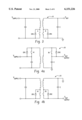
- the power conversion topology 10 requires a supply voltage V supply and outputs a bipolar output voltage V out .
- the power conversion topology 10 includes a multi-winding inductor L1 having, in the preferred embodiment, inductor winding ratios of 1:1:N.
- the supply voltage V supply is positive in this embodiment.
- the power conversion topology 10 also preferably includes four switches A, B, A1, and B1, four diodes CR1, CR2, CR3, and CR4, and an output capacitor C.
- the switch A1 is open and the switch B1 is closed.
- the diode CR1 is back-biased and not conducting (this assumption can be satisfied with proper design of turns ratio in the multi-winding inductor L1 such that the induced voltage from the secondary winding to the primary winding does not forward bias the diode).
- the resulting circuit is shown in FIG. 3.
- the topology 10 in this mode of operation reduces to that of a flyback converter 18 as shown in FIG. 3.
- the converter 18 in this operating mode produces an output voltage V out that is always positive.
- Switches A and B are driven as synchronous-rectifiers, i.e., either switch A or switch B is on at any given time, and, as a result, the converter 18 is forced into a continuous-current mode at all times.
- the output voltage V out is a function of both the supply voltage V supply ) and the duty cycle of the switches A and B where:
- V out V supply *[D/(1-D)]*N, where D is the fraction of the switching cycle when switch A is conducting and (1-D) is the fraction of the switching cycle when switch B is conducting.
- the converter 18 is operated as a continuous-current mode converter, the output voltage V out is independent of the magnitude or the direction of the output current.
- the converter 18, therefore, can produce a bi-directional output current with an output voltage V out having a positive amplitude only.
- the converter 18 is not capable of producing a negative output voltage V out .
- the switch A in another mode of operation the switch A is open and the switch B is closed.
- the diode CR3 is back-biased and not conducting (this assumption can be satisfied with proper design of turns ratio in the multi-winding inductor L1).
- the resulting circuit is shown in FIG. 4a, which is redrawn as FIG. 4b.
- the topology 10 in this mode of operation reduces to that of a flyback converter 20 that only produces negative output voltages V out .
- Switches A1 and B1 are driven as synchronous-rectifiers, i.e., either switch A1 or switch B1 is on at any given time, and, as a result, the circuit is forced into a continuous-current mode at all times.
- the output voltage Vout is a function of both the supply voltage V supply and the duty cycle of the switches A and B where:
- V out (-1)*V supply *[D/(1-D)]*N, where D is the fraction of the switching cycle when switch A1 is conducting and (1-D) is the fraction of the switching cycle when switch B1 is conducting.
- the converter output voltage V out is independent of the magnitude or the direction of the output current.
- the converter 20, therefore, can produce a bi-directional output current with an output voltage V out having a negative amplitude only.
- the converter 20 is not capable of producing a positive output voltage V out .
- the topology 10 has 4Q output capability.
- the 4Q power conversion topology 10 shown in FIG. 2 has the following features:
- the continuous-current mode converter 10 is capable of bi-directional output currents
- switch A1 is opened, switch B1 is closed, and switches A and B are driven as synchronous rectifiers;
- switch A is opened, switch B is closed, and switches A1 and B1 are driven as synchronous rectifiers;
- the magnitude of the output voltage V out is a linear function of the supply voltage V supply and is a non-linear function of switch duty cycle D;
- the multi-winding inductor L1 provides a level of galvanic isolation between the input and the output.
- the 4Q power conversion topology 10 of the present invention has many applications.
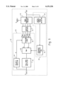
- the 4Q topology 10 can be used to construct a non-linear power amplifier 22 having four quadrant power amplification capability as shown in the block diagram of a non-linear power amplifier 22 utilizing the 4Q power conversion topology 10 of FIG. 5.
- the non-linear power amplifier 22 amplifies an input signal V sig and produces an output signal V out .
- the preferred non-linear power amplifier 22 comprises a switch-control-signal generator 23, switch drivers 32, and 4Q power conversion topology 10.
- the switch-control-signal generator 23, based on the input signal V sig , synthesizes switch activation signals A sig , B sig , A1 sig , and B1 sig that are used to control the switches A, B, A1, and B1 in the 4Q power conversion topology 10 to generate the output V out .
- the preferred switch-control-signal generator 23 comprises a polarity detector 24, a full wave rectifier 26, a pulse width modulator ("PWM") 28, and steering logic 30.
- PWM pulse width modulator
- the input signal V sig is also fullwave rectified by the full wave rectifier 26.
- the unipolar rectified signal from rectifier 26 is used by the PWM 28 to produce a pair of pulse-width-modulated logic signals D and E.
- Logic signals D and E are logical complementary waveforms with appropriate dead-time gaps for driving the synchronous rectifiers of power conversion topology 10. Stated differently, logic signal E is the logical complement of logic signal D with logic signal E's state transition occurring at a different time than logic signal D's state transition. Logic signal E falls to a low level before D rises to a high level and rises to a high level slightly after logic signal D falls to a low level.
- /V ref , where D 1 when
- V sig V ref .
- V ref is the peak-to-peak amplitude value of the frequency signal that drives the PWM 28 in this embodiment.
- the steering logic 30 uses the logic signals D and E and the polarity signal P signal to synthesize the switch activation signals A sig , B sig , A1 sig , and B1 sig that drive the switch-pairs A-B and A1-B1.
- the steering logic equations are:
- the switch drivers 32 driven by the switch activation signals A sig , B sig , A1 sig and B1 sig , perform the necessary signal conditioning to drive the power switches in power conversion topology 10.
- the 4Q power conversion topology 10 functions as described above to produce the output voltage V out .
- the amplifier output voltage V out is:
- the non-linear power amplifier of FIG. 5 has the following features:
- V out is a known, non-linear algebraic, function of V sig ;
- V out is proportional to the supply voltage, V supply ;
- V sig has both DC and AC contents
- V out will also have both DC and AC contents
- V out follows the polarity of V sig .
- An additional advantage of the preferred non-linear amplifier 22 of the present invention is a frequency modulation capability that allows the non-linear amplifier 22 to trade-off power efficiency with power supplying capability to meet dynamic load demands.
- the frequency modulator 35 performs the frequency modulation function.
- the switching frequency F of the 4Q power conversion topology 10 effects the power supplying capability and the power conversion efficiency.
- a higher switching frequency F provides greater power supplying capability but at a lower power conversion efficiency level. Therefore, the switching frequency F of the 4Q power conversion topology 10 can be chosen to minimize the size of the multi-winding inductor L1 for maximum load conditions.
- the switching frequency can be modulated according to load conditions to improve power efficiency. At nominal and light loads, efficiency and idle power can be improved by lowering the switching frequency F by a factor of about 2 to 5.
- the converter can be operated at its maximum frequency, F. Power conversion efficiencies better than 76% have been achieved at this frequency. During normal and light loads, the converter can be operated at a lower frequency, F/3, for example. The power conversion efficiencies at this frequency F/3 have been observed at better than 87%.
- the preferred frequency modulator 35 uses a peak detector 34 and a frequency modulated oscillator 36.
- the peak detector 34 measures the current through the secondary of multi-winding inductor L1 and sends a signal to oscillator 36 based on the current detected.
- the peak current is high, the oscillator 36 is caused to modulate at a higher frequency.
- the oscillator 36 is caused to modulate at a lower frequency.
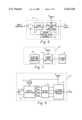
- FIGS. 6 and 7 a preferred linear power amplifier 42 and a preferred ringing generator 38 are shown.
- the general architecture of the preferred ringing generator 38 consists of a low power alerting-waveform generator 40 which drives a linear power amplifier 42.
- the linear power amplifier 42 in turn consists of a 4Q non-linear power amplifier 22 embedded in a feedback loop, as shown in FIG. 6.
- the feedback loop linearizes the 4Q non-linear amplifier 22 and regulates the output waveform V out against both supply voltage V supply variations and output load variations.
- the theory of feedback control is well-known.
- One of ordinary skill in the art could use conventional design techniques to design an appropriate feedback loop that preferably incorporates an output monitor 48 and an error amplifier 46 in a feedback loop to linearize the non-linear amplifier 22 to form the linear amplifier 42.
- One of ordinary skill in the art could also adapt the ringing generator of the present invention to other applications such as a shake table driver without departing from the spirit of the invention.
- the output voltage V out can be expressed as a function of four variables: D, P, N and V supply .
- the polarity signal P and the duty cycle signal D required to generate the desired output voltage V out can be synthesized directly because the supply voltage V supply is known by measurements and the inductor turns ratio N is known by design which leads to the following equations:
- Equations (1)-(4) can be used to translate signals P and D into switch drive logic signals A, B, A1 and B1.
- E in Eq (2) and Eq (4), is the logical complement of D with appropriate dead-time gaps for driving synchronous rectifiers.
- FIG. 8 shows an arrangement for an open loop direct synthesis high power signal generator 49.
- a crystal 50 provides a clock and frequency reference for a digital synthesizer 52.
- the digital synthesizer 52 can be designed to generate the desired signals A, B, A1 and B1.
- the switch drivers 32 and power conversion topology 10 are the same as those described with reference to the non-linear power amp 22 of FIG. 5.
- the supply voltage V supply is measured by the A/D converter 54 to account for any variance in the supply voltage V supply .
- the signal generator 49 can be provided with a frequency modulator to improve the power efficiency during non-peak load conditions.
- the frequency modulator could be constructed using direct logic synthesis or externally through a frequency modulated oscillator in place of crystal 50 or by other methods.
- V out can be generated without having to detect the polarity of any signal or without having to full-wave rectify any signal.
- crossover distortions at zero crossings due to sensing errors are eliminated.
- the signal generator 49 can be adapted to many different applications such as a ringing generator, shake table driver, and others.
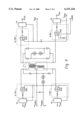
- FIGS. 9-11 show a detailed arrangement of a preferred embodiment of the linear power amp 42 of FIG. 6.
- the switch and diode pairs A1-CR1, B1-CR2, A-CR3 and B-CR4 of 4Q power converter 10 are implemented using IRF712 MOSFETs Q101, Q102, Q103, and Q104, respectively, which include a built-in diode between the substrate and source. Separate diodes CR1, CR2, CR3, and CR4 are not required if the switches A1, B1, A, and B include built-in diodes.
- Other devices could be used as switches A1, B1, A, and B, such as bipolar transistors, IGBTs, vacuum tubes, mechanical switches and relays, optical relays, light sensitive switches as well as other devices without departing from the spirit of the invention.
- the 4Q power converter 10 also includes level shifting circuits 54 which function as interfaces between the switches A1, B1, A and B and the respective switch activation signals A1 sig , B1 sig , A sig , and B sig .
- the level shifting circuits 54 may be needed because the circuits generating the switch activation signals may be referenced to a ground that is different from the 4Q power converter's primary or secondary ground references.
- the switch actuation signals are level shifted by level shifting circuits 54 so that the switches can properly respond to the switch actuation signals.
- Level shifting circuits 54 could comprise transformers or other elements to accomplish the level shifting function.
- the preferred 4Q power converter 10 is also provided with a bias voltage V Bias which is commonly used in telephonic applications.
- V Bias bias voltage
- the secondary side's ground reference in the preferred 4Q power converter 10 is referenced to the bias voltage V Bias . Consequently, the output V out of the preferred 4Q power converter 10 is biased above the bias voltage V Bias .
- the input signal for the linear power amp 42 is fed to both the polarity detector 24 and the full wave rectifier 26.
- the preferred polarity detector 24 has been implemented using a comparator U103a and the preferred full-wave rectifier 26 has been implemented using a standard op-amp full-wave rectifier circuit.
- the full-wave rectifier 26 comprises op-amps U102a and U102b which in combination with other circuit elements perform the full wave rectification function.
- the output of the full wave rectifier 26 is fed to the pulse width modulator 28.
- the PWM 28 compares, via comparator U103d, the full wave rectifier 26 output with a switching-frequency sawtooth waveform generated by the oscillator 36.
- the output of the comparator U103d is squared by the transistors Q106 and Q107 and rounded by the RC network R123-C116.
- the output of the RC network R123-C116 is then converted to the signals D and E by the comparators U103b and U103c, respectively.
- the comparators U103b and U103c provide for dead time control by generating the signals D and E such that the signal E transitions to a low state just before the signal D transitions to a high state and returns to a high state shortly after signal D returns to a low state.
- the signals D and E are then routed to the steering logic 30 along with the polarity signal P.
- the preferred steering logic 30 implements equations 1-4 using logic gates to synthesize switch activation signals A sig , B sig , A1 sig , and B1 sig . Any number of combinations of elements such as logic gates, transistors, memory units, programmable logic devices, or other devices could be used to perform the function without departing from the spirit of the invention.
- Switch activation signals A sig , B sig , A1 sig , and B1 sig are then passed to switch driver 32 which amplifies the signals A sig , B sig , A1 sig , and B1 sig so that these signals can drive the switches A, B, A1, and B1 in the 4Q power converter 10.
- the preferred switch driver 32 comprises a separate class B push-pull amplifier stage for each switch activation signal A sig , B sig , A1 sig , and B1 sig .
- the switch driver 32 could comprise many different devices such as power BJTs, power MOSFETS, power ICs and others without departing from the spirit of the invention.
- the preferred linear power amp 42 also includes an error amp 46 for linearizing the output V out .
- the preferred error amp 46 comprises a dc error amp 45 and an ac error amp 47.
- the dc error amp includes an op amp U101b that subtracts away the dc component from the output V out , namely V Bias .
- the ac error amp includes an op amp U101a which compares the ac portion of the output V out with the ac portion of the input signal.
- the ac error amp generates an error signal 51 which is fed to the full wave rectifier 26 and the polarity detector 24. If the ac portion of the output V out is the same as the input signal then the error signal 51 is equal to the input signal. If there is a difference, then the error signal 51 is adjusted so that the linear power amp 42 produces an output V out with the error eliminated.
- FIG. 11 shows a detailed arrangement of the preferred frequency modulator 35 with a preferred frequency modulated oscillator 36 and output current peak detector 34.
- the preferred output peak detector 34 is provided with an input voltage I -- sense that is proportional to the current flowing through the secondary of the multi-winding inductor L1.
- Two comparators U201a and U201b compare the I -- sense voltage to separate threshold reference voltages V T1 and V T2 . If the current flow as measured by the I -- sense voltage is more positive than a first threshold level, then the comparator U201a will output a low voltage signal. If the current flow as measured by the I -- sense voltage is more negative than a second threshold level, then comparator U201b will output a low voltage signal.
- Op amp U202a is configured as an integrator that outputs a current that drives the frequency modulator oscillator 36.
- the output current peak detector 34 is a fast attack, slow decay detector. When it senses high current flow via a high voltage the voltage I -- sense, the peak detector 34 quickly outputs a high current through op amp U202a. The current gradually reduces if the current flow through the multi-winding inductor secondary returns to a low level as measured by the voltage I -- sense.
- the preferred frequency modulated oscillator 36 comprises an opto-isolator U203, a transistor Q201 and a 555 timer U204.
- the frequency output by the 555 timer U204 is used by the PWM 28.
- the frequency is varied by the current flowing through the transistor Q201.
- the current flowing through the transistor Q201 is determined by the current flowing through the opto-isolator U203. A higher current flow through the opto-isolator U203 will result in a higher current flow through the transistor Q201 which in turn will result in a higher frequency output by the 555 timer U204.
- the current flow through the opto-isolator U203 will be high when the current flow through op-amp U202a is high which in turn occurs when the current flow through the secondary of the multi-winding inductor L1 is high.
- the 555 timer U204 will output a higher frequency when the current flow through the secondary of multi-winding inductor L1 is high.
Abstract
Description
A.sub.sig =(D AND P); (1)
B.sub.sig =(E AND P) OR (/P); (2)
A1.sub.sig =(D AND /P); (3)
B1.sub.sig =(E AND /P) OR (P). (4)
V.sub.out =[(-1)**(P+1)]*[|V.sub.sig |/(V.sub.ref -|V.sub.sig |)]*V.sub.supply *N (5)
=[(-1)**(P+1)]*[D/(1-D)]*V.sub.supply *N. (6)
P=(1/2)*(1+V.sub.out /|V.sub.out |), P=[1,0].(7)
D=|V.sub.out |/[(N*V.sub.supply)+|V.sub.out |], 0≦D≦1. (8)
Claims (52)
Priority Applications (1)
| Application Number | Priority Date | Filing Date | Title |
|---|---|---|---|
| US09/305,637 US6151226A (en) | 1999-05-05 | 1999-05-05 | Four quadrant power conversion topology |
Applications Claiming Priority (1)
| Application Number | Priority Date | Filing Date | Title |
|---|---|---|---|
| US09/305,637 US6151226A (en) | 1999-05-05 | 1999-05-05 | Four quadrant power conversion topology |
Publications (1)
| Publication Number | Publication Date |
|---|---|
| US6151226A true US6151226A (en) | 2000-11-21 |
Family
ID=23181659
Family Applications (1)
| Application Number | Title | Priority Date | Filing Date |
|---|---|---|---|
| US09/305,637 Expired - Lifetime US6151226A (en) | 1999-05-05 | 1999-05-05 | Four quadrant power conversion topology |
Country Status (1)
| Country | Link |
|---|---|
| US (1) | US6151226A (en) |
Cited By (7)
| Publication number | Priority date | Publication date | Assignee | Title |
|---|---|---|---|---|
| US20040156218A1 (en) * | 2003-02-06 | 2004-08-12 | Chin-Wen Chou | Multi-period cycle-alternative switching mode power supply control device |
| US20040188706A1 (en) * | 2003-03-27 | 2004-09-30 | Jie Chang | High-power, integrated AC switch module with distributed array of hybrid devices |
| US20050062444A1 (en) * | 2003-02-06 | 2005-03-24 | Zippy Technology Corp. | Multi-period cycle-alternative switching mode power supply control device and its control method |
| US20070008756A1 (en) * | 2005-07-08 | 2007-01-11 | Djenguerian Alex B | Method and apparatus to limit maximum switch current in a switching power supply |
| US20070008753A1 (en) * | 2005-07-08 | 2007-01-11 | Kroes Derek J | Method and apparatus to limit maximum switch current in a switch of a switching power supply |
| US20070121619A1 (en) * | 2005-11-30 | 2007-05-31 | Kimbrough Mahlon D | Communications distribution system |
| US9095054B1 (en) * | 2012-10-12 | 2015-07-28 | Arkansas Power Electronics International, Inc. | High temperature equalized electrical parasitic power packaging method for many paralleled semiconductor power devices |
Citations (3)
| Publication number | Priority date | Publication date | Assignee | Title |
|---|---|---|---|---|
| US3896395A (en) * | 1974-07-18 | 1975-07-22 | Bell Telephone Labor Inc | Linear amplification using quantized envelope components to phase reverse modulate quadrature reference signals |
| US5109185A (en) * | 1989-09-29 | 1992-04-28 | Ball Newton E | Phase-controlled reversible power converter presenting a controllable counter emf to a source of an impressed voltage |
| US5946202A (en) * | 1997-01-24 | 1999-08-31 | Baker Hughes Incorporated | Boost mode power conversion |
-
1999
- 1999-05-05 US US09/305,637 patent/US6151226A/en not_active Expired - Lifetime
Patent Citations (3)
| Publication number | Priority date | Publication date | Assignee | Title |
|---|---|---|---|---|
| US3896395A (en) * | 1974-07-18 | 1975-07-22 | Bell Telephone Labor Inc | Linear amplification using quantized envelope components to phase reverse modulate quadrature reference signals |
| US5109185A (en) * | 1989-09-29 | 1992-04-28 | Ball Newton E | Phase-controlled reversible power converter presenting a controllable counter emf to a source of an impressed voltage |
| US5946202A (en) * | 1997-01-24 | 1999-08-31 | Baker Hughes Incorporated | Boost mode power conversion |
Cited By (18)
| Publication number | Priority date | Publication date | Assignee | Title |
|---|---|---|---|---|
| US7224592B2 (en) | 2003-02-06 | 2007-05-29 | Zippy Technology Corp. | Multi-period cycle-alternative switching mode power supply control device and its control method |
| US6839253B2 (en) * | 2003-02-06 | 2005-01-04 | Zippy Technology Corp. | Multi-period cycle-alternative switching mode power supply control device |
| US20050062444A1 (en) * | 2003-02-06 | 2005-03-24 | Zippy Technology Corp. | Multi-period cycle-alternative switching mode power supply control device and its control method |
| US20040156218A1 (en) * | 2003-02-06 | 2004-08-12 | Chin-Wen Chou | Multi-period cycle-alternative switching mode power supply control device |
| US20040188706A1 (en) * | 2003-03-27 | 2004-09-30 | Jie Chang | High-power, integrated AC switch module with distributed array of hybrid devices |
| US7034345B2 (en) * | 2003-03-27 | 2006-04-25 | The Boeing Company | High-power, integrated AC switch module with distributed array of hybrid devices |
| US7894222B2 (en) | 2005-07-08 | 2011-02-22 | Power Integrations, Inc. | Method and apparatus to limit maximum switch current in a switching power supply |
| US20070008753A1 (en) * | 2005-07-08 | 2007-01-11 | Kroes Derek J | Method and apparatus to limit maximum switch current in a switch of a switching power supply |
| US7593245B2 (en) * | 2005-07-08 | 2009-09-22 | Power Integrations, Inc. | Method and apparatus to limit maximum switch current in a switching power supply |
| US7613019B2 (en) | 2005-07-08 | 2009-11-03 | Power Integrations, Inc. | Method and apparatus to limit maximum switch current in a switch of a switching power supply |
| US20090296427A1 (en) * | 2005-07-08 | 2009-12-03 | Power Integrations, Inc. | Method and apparatus to limit maximum switch current in a switching power supply |
| US20070008756A1 (en) * | 2005-07-08 | 2007-01-11 | Djenguerian Alex B | Method and apparatus to limit maximum switch current in a switching power supply |
| US20110110125A1 (en) * | 2005-07-08 | 2011-05-12 | Power Integrations, Inc. | Method and apparatus to limit maximum switch current in a switching power supply |
| US8089781B2 (en) | 2005-07-08 | 2012-01-03 | Power Integrations, Inc. | Method and apparatus to limit maximum switch current in a switching power supply |
| US8325498B2 (en) | 2005-07-08 | 2012-12-04 | Power Integrations, Inc. | Method and apparatus to limit maximum switch current in a switching power supply |
| US8477515B2 (en) | 2005-07-08 | 2013-07-02 | Power Integrations, Inc. | Method and apparatus to limit maximum switch current in a switching power supply |
| US20070121619A1 (en) * | 2005-11-30 | 2007-05-31 | Kimbrough Mahlon D | Communications distribution system |
| US9095054B1 (en) * | 2012-10-12 | 2015-07-28 | Arkansas Power Electronics International, Inc. | High temperature equalized electrical parasitic power packaging method for many paralleled semiconductor power devices |
Similar Documents
| Publication | Publication Date | Title |
|---|---|---|
| US4479175A (en) | Phase modulated switchmode power amplifier and waveform generator | |
| US8971082B2 (en) | Power conditioning unit with voltage converters | |
| JP3260024B2 (en) | Power circuit | |
| US6388514B1 (en) | Class D high voltage amplifier system with adaptive power supply | |
| US7952426B2 (en) | Digital audio amplifier and digital audio amplifying method therefor | |
| US6483731B1 (en) | Alexander topology resonance energy conversion and inversion circuit utilizing a series capacitance multi-voltage resonance section | |
| US6807073B1 (en) | Switching type power converter circuit and method for use therein | |
| US5986498A (en) | Audio direct from power supply | |
| JP4735826B2 (en) | Power converter | |
| US20070126372A1 (en) | Power supply devices | |
| US6282111B1 (en) | Inverter control using current mode slope modulation | |
| JPH06502294A (en) | High power factor voltage doubler rectifier | |
| JPS6130963A (en) | On-line switching mode power source | |
| US5896280A (en) | Frequency converter and improved UPS employing the same | |
| JPH07115774A (en) | Power supply | |
| US6151226A (en) | Four quadrant power conversion topology | |
| KR101041913B1 (en) | Polyphase impedance transformation amplifier | |
| JP2004088730A (en) | Efficient power amplifier | |
| US20070133232A1 (en) | Technique to improve dynamic response of two-stage converters | |
| US7015754B2 (en) | Isolated converter with synchronized switching leg | |
| KR100608001B1 (en) | Apparatus and method for limiting current of audio amplifier | |
| Ljusev et al. | Direct-conversion switching-mode audio power amplifier with active capacitive voltage clamp | |
| JP2603646B2 (en) | converter | |
| JP2001320880A (en) | Rectifying power supply | |
| KR101880544B1 (en) | Smps for power amp based on compensation of ripple voltage and control method thereof |
Legal Events
| Date | Code | Title | Description |
|---|---|---|---|
| AS | Assignment |
Owner name: RELTEC CORPORATION, OHIO Free format text: ASSIGNMENT OF ASSIGNORS INTEREST;ASSIGNORS:CHEN, WILLIAM I. H.;YANCEY, EDWIN GLENN;KIMBROUGH, MAHLON DANNY;REEL/FRAME:009954/0835 Effective date: 19990427 |
|
| AS | Assignment |
Owner name: MARCONI COMMUNICATIONS, INC., OHIO Free format text: CHANGE OF NAME;ASSIGNOR:RELTEC CORPORATION;REEL/FRAME:010043/0815 Effective date: 19990531 |
|
| STCF | Information on status: patent grant |
Free format text: PATENTED CASE |
|
| AS | Assignment |
Owner name: MARCONI INTELLECTUAL PROPERTY (RINGFENCE)INC., PEN Free format text: ASSIGNMENT OF ASSIGNORS INTEREST;ASSIGNOR:MARCONI COMMUNICATIONS, INC.;REEL/FRAME:014646/0607 Effective date: 20031028 |
|
| AS | Assignment |
Owner name: ADVANCED FIBRE ACCESS CORPORATION, CALIFORNIA Free format text: ASSIGNMENT OF ASSIGNORS INTEREST;ASSIGNOR:MARCONI INTELLECTUAL PROPERTY (RINGFENCE), INC.;REEL/FRAME:014532/0723 Effective date: 20040220 |
|
| FPAY | Fee payment |
Year of fee payment: 4 |
|
| AS | Assignment |
Owner name: TELLABS BEDFORD, INC., TEXAS Free format text: CHANGE OF NAME;ASSIGNOR:ADVANCED FIBRE ACCESS CORPORATION;REEL/FRAME:016269/0577 Effective date: 20041208 |
|
| AS | Assignment |
Owner name: MARCONI COMMUNICATIONS INC., OHIO Free format text: CORRECTIVE ASSIGNMENT TO CORRECT THE RELTEC CORPORATION TO RELTEC COMMUNICATIONS INC. AND MARCONI COMMUNICATIONS, INC. TO MARCONI COMMUNICATIONS INC. PREVIOUSLY RECORDED ON REEL 010043 FRAME 0815;ASSIGNOR:RELTEC COMMUNICATIONS INC.;REEL/FRAME:018282/0811 Effective date: 19990531 |
|
| FEPP | Fee payment procedure |
Free format text: PAYOR NUMBER ASSIGNED (ORIGINAL EVENT CODE: ASPN); ENTITY STATUS OF PATENT OWNER: LARGE ENTITY |
|
| FPAY | Fee payment |
Year of fee payment: 8 |
|
| FEPP | Fee payment procedure |
Free format text: PAYOR NUMBER ASSIGNED (ORIGINAL EVENT CODE: ASPN); ENTITY STATUS OF PATENT OWNER: LARGE ENTITY Free format text: PAYER NUMBER DE-ASSIGNED (ORIGINAL EVENT CODE: RMPN); ENTITY STATUS OF PATENT OWNER: LARGE ENTITY |
|
| FPAY | Fee payment |
Year of fee payment: 12 |
|
| AS | Assignment |
Owner name: BANK OF AMERICA, N.A., AS ADMINISTRATIVE AGENT, TE Free format text: SECURITY INTEREST;ASSIGNOR:TELLABS ENTERPRISE, INC. (F/K/A TELLABS BEDFORD, INC.);REEL/FRAME:041233/0618 Effective date: 20161230 |