US6151347A - Laser diode and method of fabrication thereof - Google Patents
Laser diode and method of fabrication thereof Download PDFInfo
- Publication number
- US6151347A US6151347A US09/093,399 US9339998A US6151347A US 6151347 A US6151347 A US 6151347A US 9339998 A US9339998 A US 9339998A US 6151347 A US6151347 A US 6151347A
- Authority
- US
- United States
- Prior art keywords
- active region
- cells
- semiconductor
- grating
- layer
- Prior art date
- Legal status (The legal status is an assumption and is not a legal conclusion. Google has not performed a legal analysis and makes no representation as to the accuracy of the status listed.)
- Expired - Fee Related
Links
Images


Classifications
-
- B—PERFORMING OPERATIONS; TRANSPORTING
- B82—NANOTECHNOLOGY
- B82Y—SPECIFIC USES OR APPLICATIONS OF NANOSTRUCTURES; MEASUREMENT OR ANALYSIS OF NANOSTRUCTURES; MANUFACTURE OR TREATMENT OF NANOSTRUCTURES
- B82Y20/00—Nanooptics, e.g. quantum optics or photonic crystals
-
- H—ELECTRICITY
- H01—ELECTRIC ELEMENTS
- H01S—DEVICES USING THE PROCESS OF LIGHT AMPLIFICATION BY STIMULATED EMISSION OF RADIATION [LASER] TO AMPLIFY OR GENERATE LIGHT; DEVICES USING STIMULATED EMISSION OF ELECTROMAGNETIC RADIATION IN WAVE RANGES OTHER THAN OPTICAL
- H01S5/00—Semiconductor lasers
- H01S5/30—Structure or shape of the active region; Materials used for the active region
- H01S5/34—Structure or shape of the active region; Materials used for the active region comprising quantum well or superlattice structures, e.g. single quantum well [SQW] lasers, multiple quantum well [MQW] lasers or graded index separate confinement heterostructure [GRINSCH] lasers
-
- H—ELECTRICITY
- H01—ELECTRIC ELEMENTS
- H01S—DEVICES USING THE PROCESS OF LIGHT AMPLIFICATION BY STIMULATED EMISSION OF RADIATION [LASER] TO AMPLIFY OR GENERATE LIGHT; DEVICES USING STIMULATED EMISSION OF ELECTROMAGNETIC RADIATION IN WAVE RANGES OTHER THAN OPTICAL
- H01S5/00—Semiconductor lasers
- H01S5/02—Structural details or components not essential to laser action
- H01S5/0206—Substrates, e.g. growth, shape, material, removal or bonding
- H01S5/021—Silicon based substrates
-
- H—ELECTRICITY
- H01—ELECTRIC ELEMENTS
- H01S—DEVICES USING THE PROCESS OF LIGHT AMPLIFICATION BY STIMULATED EMISSION OF RADIATION [LASER] TO AMPLIFY OR GENERATE LIGHT; DEVICES USING STIMULATED EMISSION OF ELECTROMAGNETIC RADIATION IN WAVE RANGES OTHER THAN OPTICAL
- H01S5/00—Semiconductor lasers
- H01S5/20—Structure or shape of the semiconductor body to guide the optical wave ; Confining structures perpendicular to the optical axis, e.g. index or gain guiding, stripe geometry, broad area lasers, gain tailoring, transverse or lateral reflectors, special cladding structures, MQW barrier reflection layers
- H01S5/22—Structure or shape of the semiconductor body to guide the optical wave ; Confining structures perpendicular to the optical axis, e.g. index or gain guiding, stripe geometry, broad area lasers, gain tailoring, transverse or lateral reflectors, special cladding structures, MQW barrier reflection layers having a ridge or stripe structure
- H01S5/227—Buried mesa structure ; Striped active layer
- H01S5/2275—Buried mesa structure ; Striped active layer mesa created by etching
- H01S5/2277—Buried mesa structure ; Striped active layer mesa created by etching double channel planar buried heterostructure [DCPBH] laser
-
- H—ELECTRICITY
- H01—ELECTRIC ELEMENTS
- H01S—DEVICES USING THE PROCESS OF LIGHT AMPLIFICATION BY STIMULATED EMISSION OF RADIATION [LASER] TO AMPLIFY OR GENERATE LIGHT; DEVICES USING STIMULATED EMISSION OF ELECTROMAGNETIC RADIATION IN WAVE RANGES OTHER THAN OPTICAL
- H01S5/00—Semiconductor lasers
- H01S5/30—Structure or shape of the active region; Materials used for the active region
- H01S5/34—Structure or shape of the active region; Materials used for the active region comprising quantum well or superlattice structures, e.g. single quantum well [SQW] lasers, multiple quantum well [MQW] lasers or graded index separate confinement heterostructure [GRINSCH] lasers
- H01S5/3427—Structure or shape of the active region; Materials used for the active region comprising quantum well or superlattice structures, e.g. single quantum well [SQW] lasers, multiple quantum well [MQW] lasers or graded index separate confinement heterostructure [GRINSCH] lasers in IV compounds
Definitions
- This invention relates to a laser diode, and a method of fabrication thereof.
- Semiconductor lasers have an important role as light sources for optical communication systems. By selecting appropriate semiconductor materials, conventionally III-V alloy compounds, lasers which emit in the wavelength range from 0.8 ⁇ m to 1.7 ⁇ m can be fabricated. At present, long haul optical fiber communication is based on operating wavelengths around 1.55 ⁇ m and 1.3 ⁇ m, the wavelengths at which single mode optical fibers have minimum attenuation and dispersion respectively. Lasers have advantages over light emitting diodes (LEDs) of providing a coherent, narrow bandwidth source, ideally suited for communications applications.
- LEDs light emitting diodes
- Single mode, narrow linewidth light sources for optical communication are thus dominated by laser diodes fabricated from direct band gap, III-V semiconductor alloy materials, particularly InP/InGaAsP, which emit in this wavelength region.
- direct band gap, III-V semiconductor alloy materials particularly InP/InGaAsP
- MQW multiple quantum well
- 2.5 Gb/s transmission systems with a repeater span of 80 km are commercially available, and systems for practical long haul transmission at 10 Gb/s are under development.
- Shorter wavelength sources e.g. GaAs/AlGaAs which emits at 0.9 ⁇ m, are used for short distance transmission.
- Semiconductor lasers from other direct bandgap materials of group II-VI are also being developed, but these devices emit at shorter wavelength than 1.3 ⁇ m and currently exhibit poor cw lifetimes.
- GaAs integrated circuits surpass the performance of silicon based ICs for high frequency applications, their use is generally limited to specialized applications where higher performance and speed requirements offset manufacturing issues and relatively high manufacturing costs per unit.
- indirect bandgap materials including silicon and silicon-germanium, have long been considered to be incapable of efficient light emission. There is much speculation as to how, if at all, a high efficiency silicon-based light source may be fabricated, let alone whether a laser could be fabricated.
- the room temperature band gap of silicon is 1.14 eV
- Ge is 0.67 eV
- the band gap of strained Si 1-x Ge x , alloys spans the range from 1.12 to 0.6 eV, i.e. 1.1 ⁇ m to 2 ⁇ m. Strain and quantum confinement effects shift optical emission to higher energies in very thin layers (see for example, Rowell et al. J. Appl. Phys. 74(4), p. 2795, Aug. 15, 1993).
- silicon-germanium alloys are of considerable interest for silicon based optoelectronics for communication systems.
- the present invention seeks to provide a laser diode based on a group IV material, and particularly a laser diode compatible with silicon-based integrated circuits, and a method of fabrication thereof.
- a semiconductor laser device comprising:
- the active region within a laser cavity formed on the substrate, the active region comprising a quantum well of an indirect band gap semiconductor material,
- the quantum well being divided laterally into a two dimensional array of cells
- a semiconductor laser device having an active layer comprising a quantum well of an indirect band gap material is provided.
- the quantum well is laterally subdivided into a two dimensional array of cells. This is achieved practically by defining two sets of intersecting grating grooves through the quantum well layer.
- the resulting grating structure functions not only to provide gain and index coupling, but to subdivide the quantum well into localized cells or islands of small dimensions. Subdivision of the quantum wells serves to isolate the deleterious effect of non-radiative recombination to specific cells, thereby enhancing the achievable population inversion overall.
- a two dimensional periodic array also provides for combined gain-coupled and index-coupled distributed feedback.
- a semiconductor laser device structure is provided for obtaining stimulated emission and gain using an active layer comprising a quantum well of an indirect band gap material.
- the active region comprises a multi-quantum well structure.
- the indirect band gap material is provided by a layer of a group IV semiconductor material having a suitable band gap, for example, a quantum well layer of a silicon-germanium alloy, i.e., Si 1-x Ge x , where x is selected to provide a predetermined band gap.
- the quantum well structure comprises a multi-quantum well SiGe alloy/Si layer structure
- the two dimensional grating comprises a double grating structure in two independent lateral directions (not necessarily orthogonal) which divides the multiple quantum layers into an array of "cells" of finite dimensions, which extend through the SiGe alloy quantum well structure, and in which the motion of free carriers is thus restricted or localized.
- the carriers are localized within the quantum well layers, and laterally isolated by the 2 dimensional grating which defines the cell regions. This effect increases the probability of radiative recombination, in combination with the band broadening created by the finite dimensions of the cells, so that no-phonon transitions may occur, and increases the stimulated emission rate.
- the periodicity of the grating structure may be selected to correspond to a Bragg reflection condition of the desired lasing wavelength, to provide combined gain-coupled and index-coupled distributed feedback of optical power along the direction of the laser cavity fabricated from group IV materials.
- a laser having a Fabry-Perot configuration may be provided.
- the grating grooves may be etched through all or part of the active region, and beneficially an isolating layer is provided on sidewalls of the cells of the active region.
- the isolating layer e.g., a dielectric layer, is beneficial in providing a large step in index of refraction, assisting in reducing radiative recombination at the semiconductor-insulator interface, and in channelling of current through the quantum wells.
- Means for creating a population inversion comprise electrical contacts for current injection into the active region.
- the semiconductor laser device may be capable of coupling to an external optical pump source to create a population inversion.
- a semiconductor laser diode comprising:
- a silicon substrate having defined thereon a layer of a first conductivity type, an active region within a laser cavity formed on the substrate, the active region comprising at least one quantum well of an indirect bandgap material, and a layer of a second conductivity type,
- the active region being laterally subdivided into a two dimensional array of localized cells
- first and second contact regions for current injection into the active region for achieving a population inversion in cells of the active region.
- Another aspect of the present invention provides a gain coupled distributed feedback laser diode comprising:
- a substrate comprising a semiconductor layer of a first conductivity type and a semiconductor layer of a second conductivity type, and disposed therebetween an active region on the substrate comprising a silicon/silicon-germanium multi-quantum well structure;
- the grating thereby defining an array of cells of finite dimensions within the quantum well structure, said dimensions being selected to provide carrier localization within the cells, and the periodicity of the grating also providing gain coupling and distributed feedback in operation of the device at a selected wavelength.
- a gain coupled distributed feedback laser diode comprising:
- an active region on the substrate comprising a Group IV semiconductor and a Group IV semiconductor alloy multi-quantum well structure having a two dimensional grating structure defined through the active region;
- the grating defining an array of cells of finite dimensions within the quantum well structure, said dimensions being selected to provide carrier localization within the cells, and the periodicity of the grating in at least one direction providing gain coupling and distributed feedback in operation of the device at a selected wavelength of emission from the active layer.
- a method of fabricating a laser diode comprising the steps of providing a substrate, forming thereon a quantum well of an indirect bandgap semiconductor material, and laterally dividing the quantum well into a two dimensional array of cells, preferably by defining intersecting sets of grating grooves through the quantum well layer.
- the quantum well layer is provided by a group IV semiconductor alloy material.
- a multi-quantum well structure for example a silicon-germanium alloy/silicon multi-quantum well structure is fabricated on a silicon semiconductor substrate.
- the method is compatible with known ultra high vacuum (UHV) chemical vapour deposition (CVD) processes, for example, for fabricating SiGe alloy quantum well structures on silicon substrates.
- UHV ultra high vacuum
- CVD chemical vapour deposition
- the method may be adapted to form a laser device from other group IV alloy materials.
- FIG. 1 shows a schematic diagram of part of a semiconductor laser device structure according to a first embodiment of the present invention
- FIG. 2 shows an enlarged schematic cross sectional diagram detailing part of the layer structure of FIG. 1;
- FIG. 3 shows an enlarged view of a part of a partially fabricated semiconductor laser device structure represented by FIG. 1, detailing the double intersecting grating structure;
- FIGS. 4A and 4B shows schematic diagrams of the energy vs. wavevector relationship for a direct and indirect bandgap semiconductor (infinite lattice), respectively;
- FIG. 5 shows a schematic diagram of the band structure for an indirect band gap semiconductor (infinite lattice), and for an indirect bandgap semiconductor for a finite lattice of limited spatial extent;
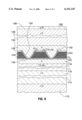
- FIG. 6 shows a schematic cross sectional diagram showing part of the layer structure of a semiconductor laser device according to a second embodiment.
- FIG. 1 A semiconductor laser device 10 according to a first embodiment of the present invention is shown schematically in FIG. 1, and FIG. 2 shows an enlarged schematic cross-section of part of the structure of FIG. 1.
- FIG. 3 shows a partially fabricated part of the structure of FIG. 1.
- the semiconductor laser device 10 is fabricated from Group IV semiconductor materials, and comprises an active layer 20 within a laser cavity formed on the substrate 12, the active layer 20 comprising a quantum well of an indirect band gap material, i.e., comprising a SiGe alloy/Si quantum well structure.
- the semiconductor laser device comprises a heavily N doped (100) silicon substrate 12, on which is defined an N doped silicon buffer layer 14 with a doping level lower than the substrate doping level.
- An optional waveguiding layer 16 comprising a SiGe alloy layer, e.g., a Si 1-y Ge y where y is ⁇ 0.05, is provided as a design optimization.
- a silicon spacer layer 18 is provided over the waveguiding layer 16.
- the active region overlies the spacer layer 18 and comprises a multi-quantum well (MQW) structure 20 which includes, for example, twelve periods of an undoped SiGe/Si quantum well layer structure comprising alternating layers 22 of SiGe alloy of a selected composition, e.g., Si 1-x Ge x where x ⁇ 0.30 (i.e., Si 0 .70 Ge 0 .30), and layers 22 of Si, each layer being e.g., 30 ⁇ thick.
- MQW multi-quantum well
- the alloy composition and layer thicknesses of the MQW structure 20 are tailored to provide specific band gap energies, to provide for lasing at a required wavelength. Increasing the number of quantum wells provides higher gain per unit length of the laser cavity. A limitation to the number of quantum wells with a specific composition is imposed by the critical thickness before formation of dislocations, which would be detrimental to device performance and/or reliability.
- a cap layer 26 of undoped silicon is formed on top of the quantum well structure 20.
- a two dimensional gain grating structure is patterned through the active region, that is, through the multi-quantum well structure to form a grating structure as shown schematically in FIG. 1.
- the two dimensional grating comprising coplanar sets of intersecting grooves 28 and 30, is defined through the quantum well layers to the underlying undoped Si spacer layer 18.
- a cross sectional view of part of the layer structure of FIG. 1 is shown on an enlarged scale in FIG. 2.
- Two intersecting sets of grating grooves are provided to define an active region comprising an array of cells, each cell 27 comprising a MQW structure, as shown schematically in FIG. 3, which shows part of the structure, up to layers in which the grating is defined.
- the grating period is the same for both gratings and the gratings are orthogonal.
- the grating period is nominally on the order of 100 nm.
- the grating period is determined by an integer multiple of ⁇ /2n where ⁇ is very close to the desired lasing wavelength, (typically within 5 nm), and n is the refractive index of the material, i.e., ⁇ 3.5 for SiGe.
- a first order grating is fabricated with a period of 188 nm (for ⁇ 1.32 ⁇ m).
- the V grooves are provided by an etch selective to revealing the ⁇ 111 ⁇ planes of the structure which are inclined at 54.4° to the (100) surface, as will be explained below.
- a layer of insulating and passivating material 32 e.g. SiO 2 lines the ⁇ 111 ⁇ planes of the grating grooves which define sidewalls of each cell, and a layer of silicon 34 fills the grating grooves.
- An upper silicon cladding layer 36, and a P + top contact layer 38 completes the structure.
- the substrate provides an N + contact layer. Electrical contacts (not shown) to the P + layer and N + substrate are provided in a conventional manner.
- the insulating layer 32 is beneficial in three respects: for providing a large step in the index of refraction for the grating, to reduce the carrier recombination velocity at the semiconductor-insulator interface to minimize non-radiative recombination, and to provide effective channeling of all current through the quantum wells.
- a gain-coupled two-dimensional grating DFB laser device is provided.
- the two intersecting gratings which in this case are orthogonal at 90°, define isolated regions or "cells" of the Si/SiGe multi-quantum well structure which have micro-structural dimensions, i.e., up to the grating period ⁇ 185 nm. Nevertheless these structures are significantly larger than the light emitting silicon based nano-structures and structures referred to as quantum dots in the above mentioned references.
- Thin film lasers using two dimensional gratings are analyzed in articles by Shyh Wang et al., Appl. Phys. Lett., Vol. 22 No. 9, May 1, 1973 entitled “Two dimensional distributed feedback lasers and their applications” and in Sov. J. Quantum Electron. 9(4) April 1979 by Luk'yanova et al. entitled "Thin film laser with a two dimensional diffraction grating".
- Evans et al "Crossed gratings for semiconductor lasers", IEEE 13th SCCD Conference 1992 (Japan) a non-orthogonal grating was used to provide an effective periodicity smaller than either of the individual gratings.
- these double grating structures have remained a curiosity in III-V light emitting materials because one dimensional grating structures have provided efficient light emission and lasers.
- the two dimensional grating serves a dual function. Firstly, the grating provides gain and index coupling in a DFB laser as described in the latter references. Secondly, the grating also subdivides the quantum well structure into cells, or islands, of small dimensions, which create carrier localization. The latter effect shortens carrier lifetimes sufficiently to obtain stimulated emission from an indirect band gap material, as explained below.
- the inherent feature of an indirect gap semiconductor is not that it exhibits inefficient light emission, but that the carrier lifetime is orders of magnitude greater than for direct gap material due to the requirement for phonon involvement, thereby allowing for sufficient time for the carriers to diffuse randomly in the material until they interact with a non-radiative defect site, even if these sites are present in concentrations below 10 14 cm -3 .
- This limitation can be overcome by restricting motion of the carriers in the quantum wells to small localized cells, thereby greatly reducing the probability that carriers can interact with a non-radiative defect site.
- the valence band discontinuity of SiGe with Si serves to trap holes in the SiGe layer.
- Restriction of motion of carriers in the lateral direction can be achieved by etching a pattern, e.g., a grating grid as described above, through the QWs to define the cell size. Passivation of the exposed surface of the QW reduces the carrier surface recombination velocity. While trapped in such cells, the carriers have no option, other than to undergo radiative recombination, or, if the carrier density in a given cell becomes exceedingly high, Auger recombination (non-radiative). In this respect the entrapment of carriers within a cell is not a "quantum confinement", but rather a localization of carriers which depends on the size of the cells being sufficiently small to provide for a large proportion of cells which do not contain a non-radiative centre.
- Optical feedback may be obtained by a Fabry Perot geometry, i.e., by introducing suitable reflective facets, in combination with the grating structure.
- optical feedback is obtained within the resonant cavity, as described above, by using the coplanar double grating structure to provide distributed feedback. In this case, the grating period in the direction of the laser cavity must satisfy a Bragg reflection condition for the intended laser wavelength.
- the device structure is gain coupled by the periodic gain/no gain structure of the grating, and supports a laser mode having a standing wave with maxima predominantly situated on the points of highest gain, i.e., one mode is very favourably situated with respect to grating structure.
- a complementary structure may be fabricated on a P type wafer.
- the waveguiding layer 16 of SiGe alloy underlying the active layer was provided as a design optimization, but optionally may be omitted.
- the two dimensional grating structure described above comprises 2 sets of coplanar, orthogonal V grooves which truncate in the silicon spacing layer underlying the QW structure.
- the V grooves extend only partly through the QW structure.
- the passivation layer within the grooves serves to redirect current through the cells.
- silicon grown on the active region will be single crystal, but silicon grown on the passivation layer will be polycrystalline. The latter, having higher resistivity, will further assist in directing current through the crystalline silicon and through the active region.
- the laser structure is similar to that of the first embodiment except for the profile of the grating grooves, which are formed by a dry etching method, i.e., by etching in a plasma.
- profile which is V shaped with a sharp vertex, resulting from a chemical etch process as described above
- the dry etch process results in a groove 130 having a V shape with a rounded vertex, as illustrated schematically in FIG. 6.
- corresponding layers of the structure are denoted by the same reference numerals, incremented by 100.
- a rectangular grating is provided, e.g., as provided by highly anisotropic reactive ion etching. It is expected to be more difficult to provide selective passivation on the bottom 100 surface of a rectangular groove compared to the 100 top surface. Lack of passivation on the bottom of the groove would allow current leakage through the groove, reducing efficiency of channelling of current through the active area.
- the functional requirements for the grating structure i.e., for subdividing the quantum well structure to provide localization of carriers, may be met with any suitable 2 dimensional grating structure, providing also that the grating periodicity in at least one dimension provides for a Bragg condition for distributed feedback to provide for lasing in the direction of the laser cavity.
- any suitable 2 dimensional grating structure providing also that the grating periodicity in at least one dimension provides for a Bragg condition for distributed feedback to provide for lasing in the direction of the laser cavity.
- 2 dimensional grating configurations e.g., a circular grating comprising concentric grooves which are subdivided radially into sections, may be contemplated. Nevertheless, more complex grating configurations may present more practical problems in their fabrication.
- reflective facets are provided to define a laser cavity having a Fabry Perot configuration.
- the grating period it is not necessary for the grating period to match the Bragg condition to provide distributed feedback and thus the grating need only provide the function of dividing the quantum well structure into the two dimensional array of isolated cells.
- the heavily doped substrate provides an N + contact layer.
- the substrate need not be heavily doped, if all electrical contacts are provided on the top (processed) surface of the waver where the active region is located.
- the semiconductor lasers of the embodiments described above are semiconductor diode laser structures, i.e., have contacts for electrical excitation of the active layer by current injection. It is also contemplated that a semiconductor laser device of yet another embodiment may be provided with optical pump means, e.g., by providing population inversion with suitable optical coupling to a another light source on the substrate.
- the Si/SiGe alloy laser diode structure of the first embodiment described above may be fabricated by adaptation of known methodology for fabrication of laser diode structures using III-V materials, by providing suitable processes for fabricating and defining layers of the required group IV, Si and SiGe alloy materials by UHV-CVD methods developed for fabrication of known SiGe alloy quantum well structures.
- the following process provides a practical method of implementing the structure of the embodiment described in detail above.
- a semiconductor silicon substrate e.g., heavily doped n-type (100) silicon, e.g. As doped 1 ⁇ 10 19 cm -3 or greater, is suitable. If required the substrate is cleaned by a conventional method, and dipped in 1% HF, (a DI water rinse and N 2 spin or blow dry was omitted) to render the surface hydrophobic.
- the prepared substrate is loaded promptly into a commercially available UHV-CVD reactor and a buffer layer of n-type silicon is grown thereon, i.e., 2.5 ⁇ m n-type 1 ⁇ 10 17 cm -3 phosphorus doped silicon, grown at 550° C., e.g., from a conventional reactant mixture of silane and a phosphorous source e.g. phosphine. Growth is terminated by suspending the reactive gas flows, and ultra high vacuum is re-established in the reactor. The growth temperature is reset to 525° C. and once a steady state temperature is reached growth is resumed to provide a layer of silicon-germanium with 1 ⁇ 10 17 phosphoris doping is grown thereon, to provide a waveguiding SiGe layer.
- a buffer layer of n-type silicon is grown thereon, i.e., 2.5 ⁇ m n-type 1 ⁇ 10 17 cm -3 phosphorus doped silicon, grown at 550° C., e.g., from a
- the SiGe layer is grown by a known method, using reactive gases comprising silane and germane in the required proportions.
- the waveguiding SiGe layer is preferably about 1600 ⁇ thick of an alloy of composition Si 0 .95 Ge 0 .05 to provide the required bandgap and refractive index.
- An overlying layer of undoped silicon is then provided to form a bottom spacer layer, about 400 ⁇ , thick.
- a series of undoped active QWs are grown, that is, as shown in FIG. 1: 12 quantum wells comprising layers of 30 ⁇ Si 0 .70 Ge 0 .3, with 11 corresponding intervening barrier layers of 30 ⁇ Si.
- An undoped silicon top spacer layer 100 ⁇ thick is formed thereon.
- the layer thicknesses of the Si/SiGe alloy quantum well stack are predetermined to provide the required band gap for light emission at a predetermined wavelength, in this example, at ⁇ 1.3 ⁇ m to 1.5 ⁇ m.
- Other factors taken into consideration include the strain/thickness product limit, e.g., as discussed in an article by D.C. Houghton et al, J. Appl. Phys. Vol. 70, p. 2136, 1990.
- the resulting structure is provided with a thin etch masking layer of a layer of silicon dioxide for reasons to be explained below, and then e.g., coated with photoresist and patterned in a conventional manner to define the required grating pattern. That is, photoresist is spin coated onto the wafer and baked.
- the wafer is rotated 90° and exposed to define a second grating.
- the second grating may have the same period as the first grating, as described in the structure of the first embodiment.
- a different grating period may be used.
- the photoresist is developed, and the resulting photoresist pattern is used as a mask for a subsequent etching to transfer the grating pattern into the oxide layer.
- the exposed regions of thin protective mask layer of silicon dioxide are removed by a known method, e.g., reactive ion etching using a CF 4 /H 2 plasma.
- the grating etch into the QW layers is then performed using an anisotropic, etch.
- an etch which is selective to reveal the ⁇ 111 ⁇ planes of the Si/SiGe alloy semiconductor crystal structure is required.
- an anisotropic wet etch process is described in U.S. Pat. No.
- V grooves 28 and 30 are defined through the MQW structure as shown schematically in FIGS. 1 and 3.
- the deepest point (vertex) of the V-groove after the etch is complete, is ideally located within the Si bottom spacer layer 18 as shown in FIG. 3. That is the etch cuts right through the SiGe quantum well structure to the underlying silicon spacer layer.
- the oxide is stripped in a 1% HF dip, as noted above for substrate surface preparation, to remove the oxide layer and to provide a hydrophobic surface. Drying by spinning or blowing N 2 may be used if required to remove etchant from the grating grooves.
- a passivation layer 32 is then provided on the ⁇ 111 ⁇ facets of the grooves.
- suitable passivation may be achieved by thermal oxidation at a maximum temperature of about 550° C., to provide a thin thermal silicon dioxide layer with a low density of interface traps.
- PE-CVD plasma enhanced CVD
- a further thickness of a good dielectric is deposited thereon by low temperature plasma deposition. e.g. 200 ⁇ of SiO 2 deposited at 300° C.
- the structure is then anisotropically etched, e.g., by reactive ion etching in a CF 4 plasma, to remove the top 200 ⁇ SiO 2 passivation from the substrate surface, leaving a thin oxide 32 on the ⁇ 111 ⁇ surfaces.
- the surface is again cleaned by a 1% HF dip, as described above to provide a hydrophobic Si surface.
- the wafer is loaded promptly into the UHV-CVD reactor and another layer 34 of undoped silicon is grown over the top of the grating teeth, e.g., 300 ⁇ to 500 ⁇ of undoped silicon grown at 550° C.
- CVD silicon deposited over the original exposed Si (100) surface should be a single crystal epitaxial layer.
- Si deposited on the oxide coated (111) faces is expected to be polycrystalline.
- the growth phase may be slow, and another method of depositing silicon at low temperature, e.g. PECVD deposition of ⁇ -silicon at 300° C. may be preferable.
- a layer of p-type silicon 36 i.e., about 2.9 ⁇ m of p-type boron doped 1.0 ⁇ 10 17 cm -3 is deposited thereon.
- a conductive contact layer of heavily doped silicon e.g. p + boron doped, silicon (1 ⁇ 10 20 cm -3 ) is formed thereon.
- a ridge mask is provided on the substrate, and the substrate is etched to define ridges.
- a sidewall dielectric is deposited thereon, vias are etched through the dielectric on top of the ridges, and a top metal contact layer is deposited.
- the backside of the wafer is lapped and polished, and backside metal contacts are provided by a conventional method.
- ridges are defined having a ridge depth of 2.5 ⁇ m to 2.9 ⁇ m, somewhat deeper than that generally used in conventional ridge waveguide lasers.
- a laser diode structure comprising a double grating structure defined by intersecting coplanar grating grooves etched throughout the SiGe MQW structure as shown schematically in FIG. 1.
- the grating grooves are preferably passivated with a good dielectric layer, e.g., comprising silicon dioxide, or silicon nitride.
- the dielectric provides a high degree of passivation and assists in channeling current through the quantum well regions.
- a suitable bandgap offset e.g., a SiGe alloy [analogous to use of a semi-insulating current blocking layer in fabrication of III-V laser diode structures] is not expected to be as effective as using a good dielectric.
- a SiGe alloy would localize only holes, not electrons, and since group IV semiconductors have lower resistivities than group III-V materials, it is expected that current channeling through the active regions would not be as effective.
- the grating structure may alternatively be defined by a suitable dry etching process, to produce grating grooves of alternative shapes, e.g., anisotropic reactive ion etching with a halogen-containing plasma.
- a suitable dry etching process to produce grating grooves of alternative shapes, e.g., anisotropic reactive ion etching with a halogen-containing plasma.
- the latter process may be used to define gratings having rectangular groove structures.
- N side down a complementary structure, i.e., reversed N and P layers may alternatively be used.
- a SiGe alloy provides the particular advantage of providing emission in the required spectral region for communications applications.
- group IV alloy materials e.g. SiGeC alloys may also form suitable active layers for the QW layers.
- Other potential alloy materials from group IV may include, for example GeSn, SiSn.
Abstract
Description
Claims (46)
Priority Applications (1)
| Application Number | Priority Date | Filing Date | Title |
|---|---|---|---|
| US09/093,399 US6151347A (en) | 1996-01-17 | 1998-06-09 | Laser diode and method of fabrication thereof |
Applications Claiming Priority (2)
| Application Number | Priority Date | Filing Date | Title |
|---|---|---|---|
| US58803996A | 1996-01-17 | 1996-01-17 | |
| US09/093,399 US6151347A (en) | 1996-01-17 | 1998-06-09 | Laser diode and method of fabrication thereof |
Related Parent Applications (1)
| Application Number | Title | Priority Date | Filing Date |
|---|---|---|---|
| US58803996A Continuation-In-Part | 1996-01-17 | 1996-01-17 |
Publications (1)
| Publication Number | Publication Date |
|---|---|
| US6151347A true US6151347A (en) | 2000-11-21 |
Family
ID=24352219
Family Applications (1)
| Application Number | Title | Priority Date | Filing Date |
|---|---|---|---|
| US09/093,399 Expired - Fee Related US6151347A (en) | 1996-01-17 | 1998-06-09 | Laser diode and method of fabrication thereof |
Country Status (1)
| Country | Link |
|---|---|
| US (1) | US6151347A (en) |
Cited By (33)
| Publication number | Priority date | Publication date | Assignee | Title |
|---|---|---|---|---|
| US6366598B1 (en) * | 1999-02-10 | 2002-04-02 | Trw Inc. | High power single mode semiconductor lasers and optical amplifiers using 2D Bragg gratings |
| US20030039287A1 (en) * | 2000-03-13 | 2003-02-27 | Koji Takahashi | Gain-coupled distributed feedback semiconductor laser device and production method therefor |
| US20030141565A1 (en) * | 2002-01-28 | 2003-07-31 | Fumihiko Hirose | Diode |
| US6645829B2 (en) | 2000-08-04 | 2003-11-11 | Amberwave Systems Corporation | Silicon wafer with embedded optoelectronic material for monolithic OEIC |
| US6678296B1 (en) * | 1999-11-05 | 2004-01-13 | Fujitsu Limited | Optical semiconductor device using a SiGeC random mixed crystal |
| US20040026685A1 (en) * | 2000-04-27 | 2004-02-12 | Shigetoshi Ito | Nitride semiconductor laser device and optical pickup apparatus therewith |
| US6711200B1 (en) * | 1999-09-07 | 2004-03-23 | California Institute Of Technology | Tuneable photonic crystal lasers and a method of fabricating the same |
| US20040109328A1 (en) * | 2002-12-06 | 2004-06-10 | Chevron U.S.A. Inc. | Optical uses of diamondoid-containing materials |
| US6826223B1 (en) * | 2003-05-28 | 2004-11-30 | The United States Of America As Represented By The Secretary Of The Navy | Surface-emitting photonic crystal distributed feedback laser systems and methods |
| US20050019955A1 (en) * | 2003-07-23 | 2005-01-27 | Dahl Jeremy E. | Luminescent heterodiamondoids as biological labels |
| US6888867B2 (en) * | 2001-08-08 | 2005-05-03 | Nobuhiko Sawaki | Semiconductor laser device and fabrication method thereof |
| US6897471B1 (en) * | 2003-11-28 | 2005-05-24 | The United States Of America As Represented By The Secretary Of The Air Force | Strain-engineered direct-gap Ge/SnxGe1-x heterodiode and multi-quantum-well photodetectors, laser, emitters and modulators grown on SnySizGe1-y-z-buffered silicon |
| US20050244125A1 (en) * | 2003-06-24 | 2005-11-03 | Ansheng Liu | Method and apparatus for phase shifting an optical beam in an optical device |
| US20060057859A1 (en) * | 2004-09-16 | 2006-03-16 | International Business Machines Corporation | Buffer layer for selective SiGe growth for uniform nucleation |
| US20070001161A1 (en) * | 2005-07-01 | 2007-01-04 | University Of Delaware | Fabrication of quantum dots embedded in three-dimensional photonic crystal lattice |
| US20070105251A1 (en) * | 2005-10-28 | 2007-05-10 | Massachusetts Institute Of Technology | Method and structure of germanium laser on silicon |
| US7280712B2 (en) | 2005-08-04 | 2007-10-09 | Intel Corporation | Method and apparatus for phase shifiting an optical beam in an optical device |
| WO2007031902A3 (en) * | 2005-09-13 | 2007-10-11 | Koninkl Philips Electronics Nv | Semiconductor light emitting device with lateral current injection in the light emitting region |
| US20070280309A1 (en) * | 2006-05-23 | 2007-12-06 | Ansheng Liu | Optical waveguide with single sided coplanar contact optical phase modulator |
| US20080298407A1 (en) * | 2004-05-17 | 2008-12-04 | Akio Ikesue | Composite Laser Element and Laser Oscillator Employing It |
| US20100207097A1 (en) * | 2009-02-17 | 2010-08-19 | Jeong Tak Oh | Nitride semiconductor light emitting device and method of manufacturing the same |
| US20110229079A1 (en) * | 2010-03-19 | 2011-09-22 | Fujitsu Limited | Optical semiconductor device and method for fabricating the optical semiconductor device |
| US20130028611A1 (en) * | 2011-07-28 | 2013-01-31 | Moshe Amit | Apparatuses for Reducing the Sensitivity of an Optical Signal to Polarization and Methods of Making and Using the Same |
| US20140131734A1 (en) * | 2011-09-29 | 2014-05-15 | Toshiba Techno Center Inc. | P-type doping layers for use with light emitting devices |
| US9490392B2 (en) | 2011-09-29 | 2016-11-08 | Toshiba Corporation | P-type doping layers for use with light emitting devices |
| WO2017041812A1 (en) * | 2015-09-11 | 2017-03-16 | Forschungsverbund Berlin E.V. | Optoelectronic device, comprising a waveguide and a semiconductor nanowire array, and method of manufacturing thereof |
| US9680054B2 (en) * | 2007-07-23 | 2017-06-13 | Samsung Electronics Co., Ltd. | Quantum dot light enhancement substrate and lighting device including same |
| US9929325B2 (en) | 2012-06-05 | 2018-03-27 | Samsung Electronics Co., Ltd. | Lighting device including quantum dots |
| US9951438B2 (en) | 2006-03-07 | 2018-04-24 | Samsung Electronics Co., Ltd. | Compositions, optical component, system including an optical component, devices, and other products |
| US10305250B2 (en) | 2017-08-23 | 2019-05-28 | The Regents Of The University Of Michigan | III-Nitride nanowire array monolithic photonic integrated circuit on (001)silicon operating at near-infrared wavelengths |
| WO2020234847A1 (en) * | 2019-05-23 | 2020-11-26 | Georgia Tech Research Corporation | Method for large scale growth and fabrication of iii-nitride devices on 2d-layered h-bn without spontaneous delamination |
| CN114336270A (en) * | 2020-09-30 | 2022-04-12 | 苏州华太电子技术有限公司 | Silicon-based semiconductor laser and manufacturing method thereof |
| US11472979B2 (en) | 2007-06-25 | 2022-10-18 | Samsung Electronics Co., Ltd. | Compositions and methods including depositing nanomaterial |
Citations (3)
| Publication number | Priority date | Publication date | Assignee | Title |
|---|---|---|---|---|
| US5313484A (en) * | 1991-06-13 | 1994-05-17 | Fujitsu Limited | Quantum box or quantum wire semiconductor structure and methods of producing same |
| JPH0794806A (en) * | 1993-09-20 | 1995-04-07 | Sony Corp | Quantum box aggregation element and light beam input/ output method |
| US5591500A (en) * | 1994-08-26 | 1997-01-07 | Nec Corporation | Information recording medium |
-
1998
- 1998-06-09 US US09/093,399 patent/US6151347A/en not_active Expired - Fee Related
Patent Citations (3)
| Publication number | Priority date | Publication date | Assignee | Title |
|---|---|---|---|---|
| US5313484A (en) * | 1991-06-13 | 1994-05-17 | Fujitsu Limited | Quantum box or quantum wire semiconductor structure and methods of producing same |
| JPH0794806A (en) * | 1993-09-20 | 1995-04-07 | Sony Corp | Quantum box aggregation element and light beam input/ output method |
| US5591500A (en) * | 1994-08-26 | 1997-01-07 | Nec Corporation | Information recording medium |
Non-Patent Citations (1)
| Title |
|---|
| Mayer et al, Electronic Materials Science: For Integrated Circuits in SI and GAAS, New York: MacMillan Publishing Co, 1990, inside back cover. (no month available), Jan. 1990. * |
Cited By (60)
| Publication number | Priority date | Publication date | Assignee | Title |
|---|---|---|---|---|
| US6366598B1 (en) * | 1999-02-10 | 2002-04-02 | Trw Inc. | High power single mode semiconductor lasers and optical amplifiers using 2D Bragg gratings |
| US6711200B1 (en) * | 1999-09-07 | 2004-03-23 | California Institute Of Technology | Tuneable photonic crystal lasers and a method of fabricating the same |
| US6678296B1 (en) * | 1999-11-05 | 2004-01-13 | Fujitsu Limited | Optical semiconductor device using a SiGeC random mixed crystal |
| US20030039287A1 (en) * | 2000-03-13 | 2003-02-27 | Koji Takahashi | Gain-coupled distributed feedback semiconductor laser device and production method therefor |
| US7016391B2 (en) * | 2000-03-13 | 2006-03-21 | Sharp Kabushiki Kaisha | Gain-coupled distributed feedback semiconductor laser device and production method therefor |
| US20040026685A1 (en) * | 2000-04-27 | 2004-02-12 | Shigetoshi Ito | Nitride semiconductor laser device and optical pickup apparatus therewith |
| US6891189B2 (en) * | 2000-04-27 | 2005-05-10 | Sharp Kabushiki Kaisha | Nitride semiconductor laser device and optical pickup apparatus therewith |
| US6677655B2 (en) * | 2000-08-04 | 2004-01-13 | Amberwave Systems Corporation | Silicon wafer with embedded optoelectronic material for monolithic OEIC |
| US6680495B2 (en) | 2000-08-04 | 2004-01-20 | Amberwave Systems Corporation | Silicon wafer with embedded optoelectronic material for monolithic OEIC |
| US6645829B2 (en) | 2000-08-04 | 2003-11-11 | Amberwave Systems Corporation | Silicon wafer with embedded optoelectronic material for monolithic OEIC |
| US6888867B2 (en) * | 2001-08-08 | 2005-05-03 | Nobuhiko Sawaki | Semiconductor laser device and fabrication method thereof |
| US20030141565A1 (en) * | 2002-01-28 | 2003-07-31 | Fumihiko Hirose | Diode |
| US20040109328A1 (en) * | 2002-12-06 | 2004-06-10 | Chevron U.S.A. Inc. | Optical uses of diamondoid-containing materials |
| US20080094724A1 (en) * | 2002-12-06 | 2008-04-24 | Chevron U.S.A. Inc. | Optical uses of diamondoid-containing materials |
| US7224532B2 (en) | 2002-12-06 | 2007-05-29 | Chevron U.S.A. Inc. | Optical uses diamondoid-containing materials |
| US20080094722A1 (en) * | 2002-12-06 | 2008-04-24 | Chevron U.S.A. Inc. | Optical uses of diamondoid-containing materials |
| US20080094723A1 (en) * | 2002-12-06 | 2008-04-24 | Chevron U.S.A. Inc. | Optical uses of diamondoid-containing materials |
| US6826223B1 (en) * | 2003-05-28 | 2004-11-30 | The United States Of America As Represented By The Secretary Of The Navy | Surface-emitting photonic crystal distributed feedback laser systems and methods |
| US20040252741A1 (en) * | 2003-05-28 | 2004-12-16 | Jerry Meyer | Surface-emitting photonic crystal distributed feedback laser systems and methods |
| US20050244125A1 (en) * | 2003-06-24 | 2005-11-03 | Ansheng Liu | Method and apparatus for phase shifting an optical beam in an optical device |
| US7127129B2 (en) * | 2003-06-24 | 2006-10-24 | Intel Corporation | Method and apparatus for phase shifting an optical beam in an optical device |
| US20050019955A1 (en) * | 2003-07-23 | 2005-01-27 | Dahl Jeremy E. | Luminescent heterodiamondoids as biological labels |
| US6897471B1 (en) * | 2003-11-28 | 2005-05-24 | The United States Of America As Represented By The Secretary Of The Air Force | Strain-engineered direct-gap Ge/SnxGe1-x heterodiode and multi-quantum-well photodetectors, laser, emitters and modulators grown on SnySizGe1-y-z-buffered silicon |
| US20080298407A1 (en) * | 2004-05-17 | 2008-12-04 | Akio Ikesue | Composite Laser Element and Laser Oscillator Employing It |
| US7960191B2 (en) * | 2004-05-17 | 2011-06-14 | Akio Ikesue | Composite laser element and laser oscillator employing it |
| US7309660B2 (en) | 2004-09-16 | 2007-12-18 | International Business Machines Corporation | Buffer layer for selective SiGe growth for uniform nucleation |
| US20060057859A1 (en) * | 2004-09-16 | 2006-03-16 | International Business Machines Corporation | Buffer layer for selective SiGe growth for uniform nucleation |
| WO2007011515A2 (en) * | 2005-07-01 | 2007-01-25 | University Of Delaware | Fabrication of quantum dots embedded in three-dimensional photonic crystal lattice |
| US20070001161A1 (en) * | 2005-07-01 | 2007-01-04 | University Of Delaware | Fabrication of quantum dots embedded in three-dimensional photonic crystal lattice |
| WO2007011515A3 (en) * | 2005-07-01 | 2009-04-23 | Univ Delaware | Fabrication of quantum dots embedded in three-dimensional photonic crystal lattice |
| US7280712B2 (en) | 2005-08-04 | 2007-10-09 | Intel Corporation | Method and apparatus for phase shifiting an optical beam in an optical device |
| WO2007031902A3 (en) * | 2005-09-13 | 2007-10-11 | Koninkl Philips Electronics Nv | Semiconductor light emitting device with lateral current injection in the light emitting region |
| US20090191658A1 (en) * | 2005-09-13 | 2009-07-30 | Koninklijke Philips Electronics N.V. | Semiconductor light emitting device with lateral current injection in the light emitting region |
| US8026117B2 (en) | 2005-09-13 | 2011-09-27 | Philips Lumides Lighting Company LLC | Semiconductor light emitting device with lateral current injection in the light emitting region |
| US7596158B2 (en) * | 2005-10-28 | 2009-09-29 | Massachusetts Institute Of Technology | Method and structure of germanium laser on silicon |
| US20070105251A1 (en) * | 2005-10-28 | 2007-05-10 | Massachusetts Institute Of Technology | Method and structure of germanium laser on silicon |
| US9951438B2 (en) | 2006-03-07 | 2018-04-24 | Samsung Electronics Co., Ltd. | Compositions, optical component, system including an optical component, devices, and other products |
| US20070280309A1 (en) * | 2006-05-23 | 2007-12-06 | Ansheng Liu | Optical waveguide with single sided coplanar contact optical phase modulator |
| US11866598B2 (en) | 2007-06-25 | 2024-01-09 | Samsung Electronics Co., Ltd. | Compositions and methods including depositing nanomaterial |
| US11472979B2 (en) | 2007-06-25 | 2022-10-18 | Samsung Electronics Co., Ltd. | Compositions and methods including depositing nanomaterial |
| US20170271554A1 (en) * | 2007-07-23 | 2017-09-21 | Samsung Electronics Co., Ltd. | Quantum dot light enhancement substrate and lighting device including same |
| US10096744B2 (en) * | 2007-07-23 | 2018-10-09 | Samsung Electronics Co., Ltd. | Quantum dot light enhancement substrate and lighting device including same |
| US9680054B2 (en) * | 2007-07-23 | 2017-06-13 | Samsung Electronics Co., Ltd. | Quantum dot light enhancement substrate and lighting device including same |
| US20100207097A1 (en) * | 2009-02-17 | 2010-08-19 | Jeong Tak Oh | Nitride semiconductor light emitting device and method of manufacturing the same |
| US8030640B2 (en) * | 2009-02-17 | 2011-10-04 | Samsung Led Co., Ltd. | Nitride semiconductor light emitting device and method of manufacturing the same |
| US20110229079A1 (en) * | 2010-03-19 | 2011-09-22 | Fujitsu Limited | Optical semiconductor device and method for fabricating the optical semiconductor device |
| US9184558B2 (en) * | 2010-03-19 | 2015-11-10 | Fujitsu Limited | Optical semiconductor device and method for fabricating the optical semiconductor device |
| US8824842B2 (en) * | 2010-03-19 | 2014-09-02 | Fujitsu Limited | Optical semiconductor device and method for fabricating the optical semiconductor device |
| US20140321493A1 (en) * | 2010-03-19 | 2014-10-30 | Fujitsu Limited | Optical semiconductor device and method for fabricating the optical semiconductor device |
| US9164247B2 (en) * | 2011-07-28 | 2015-10-20 | Source Photonics, Inc. | Apparatuses for reducing the sensitivity of an optical signal to polarization and methods of making and using the same |
| US20130028611A1 (en) * | 2011-07-28 | 2013-01-31 | Moshe Amit | Apparatuses for Reducing the Sensitivity of an Optical Signal to Polarization and Methods of Making and Using the Same |
| US9178114B2 (en) * | 2011-09-29 | 2015-11-03 | Manutius Ip, Inc. | P-type doping layers for use with light emitting devices |
| US9490392B2 (en) | 2011-09-29 | 2016-11-08 | Toshiba Corporation | P-type doping layers for use with light emitting devices |
| US20140131734A1 (en) * | 2011-09-29 | 2014-05-15 | Toshiba Techno Center Inc. | P-type doping layers for use with light emitting devices |
| US9929325B2 (en) | 2012-06-05 | 2018-03-27 | Samsung Electronics Co., Ltd. | Lighting device including quantum dots |
| WO2017041812A1 (en) * | 2015-09-11 | 2017-03-16 | Forschungsverbund Berlin E.V. | Optoelectronic device, comprising a waveguide and a semiconductor nanowire array, and method of manufacturing thereof |
| US10305250B2 (en) | 2017-08-23 | 2019-05-28 | The Regents Of The University Of Michigan | III-Nitride nanowire array monolithic photonic integrated circuit on (001)silicon operating at near-infrared wavelengths |
| WO2020234847A1 (en) * | 2019-05-23 | 2020-11-26 | Georgia Tech Research Corporation | Method for large scale growth and fabrication of iii-nitride devices on 2d-layered h-bn without spontaneous delamination |
| CN114336270A (en) * | 2020-09-30 | 2022-04-12 | 苏州华太电子技术有限公司 | Silicon-based semiconductor laser and manufacturing method thereof |
| CN114336270B (en) * | 2020-09-30 | 2023-11-24 | 苏州华太电子技术股份有限公司 | Silicon-based semiconductor laser and manufacturing method thereof |
Similar Documents
| Publication | Publication Date | Title |
|---|---|---|
| US6151347A (en) | Laser diode and method of fabrication thereof | |
| EP0544408B1 (en) | Quantum confinement semiconductor light emitting devices | |
| US10008827B2 (en) | Tensile strained semiconductor photon emission and detection devices and integrated photonics system | |
| CN104769467B (en) | Semiconductor device | |
| US8111729B2 (en) | Multi-wavelength hybrid silicon laser array | |
| US20080187018A1 (en) | Distributed feedback lasers formed via aspect ratio trapping | |
| EP1742314A2 (en) | Buried heterostructure device having integrated waveguide grating fabricated by single step MOCVD | |
| US9966735B2 (en) | III-V lasers with integrated silicon photonic circuits | |
| US5677922A (en) | Semiconductor laser with crystalline window layer | |
| US6023354A (en) | Semiconductor Bragg reflector and a method of fabricating said reflector | |
| US4270096A (en) | Semiconductor laser device | |
| US11056856B2 (en) | Plasmonic laser | |
| CN108054634A (en) | A kind of narrow linewidth semiconductor laser | |
| CN113241585A (en) | Semiconductor tunable laser and preparation method thereof | |
| US9871341B2 (en) | Laser on silicon made with 2D material gain medium | |
| CN108400523B (en) | High-speed integrated DFB semiconductor laser chip and preparation method thereof | |
| US4974036A (en) | Semiconductor superlattice heterostructures on nonplanar substrates | |
| JPH0685458B2 (en) | Method of manufacturing a laser having a mirror facet | |
| US20080095491A1 (en) | Integrated Optical Wave Guide for Light Generated by a Bipolar Transistor | |
| US10944235B2 (en) | Method for producing a light source and light source | |
| Shi et al. | Flip-chip bonded evanescently coupled III-V-on-Si single-mode laser with slotted feedback structure | |
| US10389090B2 (en) | Lateral growth of edge-emitting lasers | |
| CN113594852B (en) | Narrow-linewidth semiconductor device and preparation method thereof | |
| WO2023012925A1 (en) | Semiconductor optical device and method for producing same | |
| US20210083453A1 (en) | Fabrication of ellipsoidal or semi-ellipsoidal semiconductor structures |
Legal Events
| Date | Code | Title | Description |
|---|---|---|---|
| AS | Assignment |
Owner name: NORTEL TECHNOLOGY LIMITED, CANADA Free format text: ASSIGNMENT OF ASSIGNORS INTEREST;ASSIGNORS:NOEL, JEAN-PAUL F.;ADAMS, DAVID M.;REEL/FRAME:009487/0181 Effective date: 19980721 |
|
| AS | Assignment |
Owner name: NORTEL NETWORKS CORPORATION, CANADA Free format text: CHANGE OF NAME;ASSIGNOR:NORTHERN TELECOM LIMITED;REEL/FRAME:010473/0920 Effective date: 19990429 |
|
| AS | Assignment |
Owner name: NORTEL NETWORKS CORPORATION, CANADA Free format text: CHANGE OF NAME;ASSIGNOR:NORTHERN TELECOM LIMITED;REEL/FRAME:010567/0001 Effective date: 19990429 |
|
| AS | Assignment |
Owner name: NORTEL NETWORKS LIMITED, CANADA Free format text: CHANGE OF NAME;ASSIGNOR:NORTEL NETWORKS CORPORATION;REEL/FRAME:011195/0706 Effective date: 20000830 Owner name: NORTEL NETWORKS LIMITED,CANADA Free format text: CHANGE OF NAME;ASSIGNOR:NORTEL NETWORKS CORPORATION;REEL/FRAME:011195/0706 Effective date: 20000830 |
|
| AS | Assignment |
Owner name: BOOKHAM TECHNOLOGY PLC, UNITED KINGDOM Free format text: ASSIGNMENT OF ASSIGNORS INTEREST;ASSIGNOR:NORTEL NETWORKS CORPORATION;REEL/FRAME:013678/0050 Effective date: 20021218 |
|
| AS | Assignment |
Owner name: NORTEL NETWORKS CORPORATION, ONTARIO Free format text: SECURITY INTEREST;ASSIGNORS:BOOKHAM TECHNOLOGY PLC;BOOKHAM TECHNOLOGY, INC.;BOOKHAM ACQUISITION, INC.;AND OTHERS;REEL/FRAME:013691/0552 Effective date: 20021108 |
|
| FPAY | Fee payment |
Year of fee payment: 4 |
|
| AS | Assignment |
Owner name: NORTEL NETWORKS UK LIMITED, ENGLAND Free format text: ASSIGNMENT OF ASSIGNORS INTEREST;ASSIGNOR:BOOKHAM, INC.;REEL/FRAME:016309/0469 Effective date: 20041202 |
|
| AS | Assignment |
Owner name: BOOKHAM (US), INC., CALIFORNIA Free format text: PATENT SECURITY AGREEMENT TERMINATION UNDER REEL 016309 FRAME 0469;ASSIGNOR:NORTEL NETWORKS UK LIMITED;REEL/FRAME:017097/0822 Effective date: 20060116 Owner name: BOOKHAM (CANADA) INC., CANADA Free format text: PATENT SECURITY AGREEMENT TERMINATION UNDER REEL 016309 FRAME 0469;ASSIGNOR:NORTEL NETWORKS UK LIMITED;REEL/FRAME:017097/0822 Effective date: 20060116 Owner name: BOOKHAM ACQUISITION, INC., UNITED KINGDOM Free format text: PATENT SECURITY AGREEMENT TERMINATION UNDER REEL 013691 FRAME 0552;ASSIGNOR:NORTEL NETWORKS CORPORATION;REEL/FRAME:017097/0770 Effective date: 20060118 Owner name: BOOKHAM TECHNOLOGY PLC, UNITED KINGDOM Free format text: PATENT SECURITY AGREEMENT TERMINATION UNDER REEL 016309 FRAME 0469;ASSIGNOR:NORTEL NETWORKS UK LIMITED;REEL/FRAME:017097/0822 Effective date: 20060116 Owner name: BOOKHAM (SWITZERLAND) AG, SWITZERLAND Free format text: PATENT SECURITY AGREEMENT TERMINATION UNDER REEL 013691 FRAME 0552;ASSIGNOR:NORTEL NETWORKS CORPORATION;REEL/FRAME:017097/0770 Effective date: 20060118 Owner name: BOOKHAM TECHNOLOGY PLC, UNITED KINGDOM Free format text: PATENT SECURITY AGREEMENT TERMINATION UNDER REEL 013691 FRAME 0552;ASSIGNOR:NORTEL NETWORKS CORPORATION;REEL/FRAME:017097/0770 Effective date: 20060118 Owner name: BOOKHAM (SWITZERLAND) AG, SWITZERLAND Free format text: PATENT SECURITY AGREEMENT TERMINATION UNDER REEL 016309 FRAME 0469;ASSIGNOR:NORTEL NETWORKS UK LIMITED;REEL/FRAME:017097/0822 Effective date: 20060116 Owner name: BOOKHAM TECHNOLOGY, INC., MARYLAND Free format text: PATENT SECURITY AGREEMENT TERMINATION UNDER REEL 013691 FRAME 0552;ASSIGNOR:NORTEL NETWORKS CORPORATION;REEL/FRAME:017097/0770 Effective date: 20060118 Owner name: BOOKHAM, INC., CALIFORNIA Free format text: PATENT SECURITY AGREEMENT TERMINATION UNDER REEL 016309 FRAME 0469;ASSIGNOR:NORTEL NETWORKS UK LIMITED;REEL/FRAME:017097/0822 Effective date: 20060116 |
|
| AS | Assignment |
Owner name: WELLS FARGO FOOTHILL, INC.,CALIFORNIA Free format text: SECURITY AGREEMENT;ASSIGNOR:BOOKHAM TECHNOLOGY, PLC;REEL/FRAME:018524/0089 Effective date: 20060802 Owner name: WELLS FARGO FOOTHILL, INC., CALIFORNIA Free format text: SECURITY AGREEMENT;ASSIGNOR:BOOKHAM TECHNOLOGY, PLC;REEL/FRAME:018524/0089 Effective date: 20060802 |
|
| AS | Assignment |
Owner name: BOOKHAM TECHNOLOGY PLC, UNITED KINGDOM Free format text: ASSIGNMENT OF ASSIGNORS INTEREST;ASSIGNOR:NORTEL NETWORKS LIMITED;REEL/FRAME:019920/0810 Effective date: 20021108 |
|
| REMI | Maintenance fee reminder mailed | ||
| LAPS | Lapse for failure to pay maintenance fees | ||
| STCH | Information on status: patent discontinuation |
Free format text: PATENT EXPIRED DUE TO NONPAYMENT OF MAINTENANCE FEES UNDER 37 CFR 1.362 |
|
| FP | Lapsed due to failure to pay maintenance fee |
Effective date: 20081121 |