US6151364A - Codec supporting PCM modem communications over a universal digital loop carrier - Google Patents
Codec supporting PCM modem communications over a universal digital loop carrier Download PDFInfo
- Publication number
- US6151364A US6151364A US09/183,709 US18370998A US6151364A US 6151364 A US6151364 A US 6151364A US 18370998 A US18370998 A US 18370998A US 6151364 A US6151364 A US 6151364A
- Authority
- US
- United States
- Prior art keywords
- digital
- analog
- line interface
- codec
- pcm
- Prior art date
- Legal status (The legal status is an assumption and is not a legal conclusion. Google has not performed a legal analysis and makes no representation as to the accuracy of the status listed.)
- Expired - Fee Related
Links
Images
Classifications
-
- H—ELECTRICITY
- H04—ELECTRIC COMMUNICATION TECHNIQUE
- H04B—TRANSMISSION
- H04B14/00—Transmission systems not characterised by the medium used for transmission
- H04B14/02—Transmission systems not characterised by the medium used for transmission characterised by the use of pulse modulation
- H04B14/04—Transmission systems not characterised by the medium used for transmission characterised by the use of pulse modulation using pulse code modulation
-
- H—ELECTRICITY
- H04—ELECTRIC COMMUNICATION TECHNIQUE
- H04L—TRANSMISSION OF DIGITAL INFORMATION, e.g. TELEGRAPHIC COMMUNICATION
- H04L25/00—Baseband systems
- H04L25/38—Synchronous or start-stop systems, e.g. for Baudot code
- H04L25/40—Transmitting circuits; Receiving circuits
- H04L25/49—Transmitting circuits; Receiving circuits using code conversion at the transmitter; using predistortion; using insertion of idle bits for obtaining a desired frequency spectrum; using three or more amplitude levels ; Baseband coding techniques specific to data transmission systems
- H04L25/4917—Transmitting circuits; Receiving circuits using code conversion at the transmitter; using predistortion; using insertion of idle bits for obtaining a desired frequency spectrum; using three or more amplitude levels ; Baseband coding techniques specific to data transmission systems using multilevel codes
- H04L25/4927—Transmitting circuits; Receiving circuits using code conversion at the transmitter; using predistortion; using insertion of idle bits for obtaining a desired frequency spectrum; using three or more amplitude levels ; Baseband coding techniques specific to data transmission systems using multilevel codes using levels matched to the quantisation levels of the channel
Definitions
- the present invention relates generally to the field of telephony. More specifically, the present invention discloses a codec for supporting PCM modem communications and conventional voice communications over a universal digital loop carrier.
- V.90 protocol adopted by the International Telecommunications Union (ITU) provides a specification for downstream modem data transfer rates up to 56 Kbps over the standard public switched telephone network (PSTN).
- PSTN public switched telephone network
- public switched telephone network or "PSTN” are used herein as these terms are commonly used in the United States to refer generally to the digital network between telephone company central offices.
- V.90, X2, K56flex, and other PCM modem systems overcome the limitations imposed on previous analog modems by exploiting the digital connection that most data service providers and internet service providers (ISPs) use at their end to connect to the PSTN.
- ISPs internet service providers
- the PSTN was designed for voice communications. By artificially limiting the sound spectrum to just those frequencies relevant to human speech understanding, the required bandwidth for each voice channel could be reduced, thereby increasing the number of voice channels that can be handled simultaneously when multiplexing is used. While this works well for voice communications, it imposes limits on data communications.
- existing V.34 modems that use conventional phase and amplitude modulation are optimized for the situation where both ends connect by analog lines to the PSTN, and are based on the assumption that both ends of the connection suffer impairment due to quantization noise introduced by analog-to-digital converters (ADCs).
- ADCs analog-to-digital converters
- the ADC samples the incoming analog waveform 8,000 times per second and outputs a pulse code modulation (PCM) code for each sample.
- PCM pulse code modulation
- the sampling system uses 256 discrete 8-bit PCM codes.
- the PCM codes sent across the PSTN can only approximate the original analog waveform because the sample values must be one of the 256 discrete codes.
- quantization noise The amplitude difference between the original waveform and the reconstructed quantized waveform is called quantization noise.
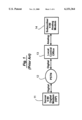
- FIG. 1 provides a diagram of a typical V.90 communications configuration.
- the high speed data direction for V.90 modems is from the central server modem 11 to the subscriber modem 14 (i.e., left to right in FIG. 1).
- the server modem 11 could be a gateway to an internet service provider (ISP) as this example shows.
- ISP internet service provider
- V.90 digital modem 11 If there are no analog-to-digital conversions between the V.90 digital modem 11 and the PSTN 12, and since the V.90 digital modem uses only the 256 discrete PCM codes available on the digital portion of the phone network, then this exact digital information reaches the subscriber's CO line interface 13, and can be correctly decoded by the subscriber's analog modem 14, without information being lost in the conversion process.
- the encoding process in the server modem 11 uses only the 256 PCM codes (or a subset) used in the digital portion of the phone network. This avoids the quantization noise that would be associated with an analog-to-digital conversion.
- the PCM codes are converted at the local telephone company's central office (CO) 13 to an analog signal that is sent to the subscriber's analog modem via a copper pair.
- the subscriber's analog modem 14 reconstructs the PCM codes from the analog signals it receives, decoding what the ISP 11 sent with no resulting loss of information.
- V.90 encoder uses various subsets of the 256 codes to eliminate detection errors between DAC output signals most susceptible to noise.
- the output of the DAC is band limited to about 3500 Hz by a reconstruction filter and connecting circuits that reduce the channel capacity (twice the available bandwidth) to approximately 7000 symbols per second. The limited bandwidth makes the symbols more difficult to distinguish from one another, a problem known as inter-symbol interference, or ISI. Therefore, the V.90 downstream modulator interleaves symbols periodically that contain lower information content, but serve to mitigate ISI.
- the V.90 protocol is asymmetrical. As previously discussed, the V.90 protocol is capable of downstream data rates of 56 Kbps because little information is lost in the digital-to-analog conversion. However, upstream communications go through an analog-to-digital conversion in the telephone company central office line interface, which under V.90 does not have the ability to support PCM symbols and thus limits the channel to lower data rates. For this reason, V.90 modems limit upstream communications to V.34 speeds.
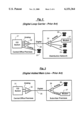
- the local exchange carrier may extend a digital carrier or a digital subscriber line (DSL) 25 from the central office to a remote terminal 24 in the subscriber's area, as illustrated in FIG. 2.
- DSL digital subscriber line
- Analog loops are then extended from the remote terminal 24 to each of the subscribers 26-29 in the carrier service area.
- this type of system is commonly known as a digital loop carrier or DLC.
- DLC digital loop carrier
- Smaller configurations are sometimes referred to as a "mini DLC.”
- the universal DLC (or UDLC) shown in FIG. 2 works well for voice communications and is satisfactory for data communications at V.34 speeds or lower. But, this type of DLC is incapable of V.90 communications due to the analog or "universal" interface between the central office switch 21 and the central office terminal 22 (COT) at the headend of the digital facility. As previously discussed, this analog interface requires an analog-to-digital conversion at the CO terminal 22 resulting in quantization noise.
- the analog interface is largely the result of the historical design for CO switches, that were based on directly providing analog loops to individual subscribers 23. Many newer CO switches are capable of providing a digital interface for a DLC, but many existing switches are not, and would require expensive retrofitting or replacement.
- a subscriber line multiplexer, universal digital carrier (UDC), or digital added main line can be used to provide additional lines over a single pair of wires as depicted in FIG. 3.
- a digital facility in this case a DSL 35, is extended from the central office to a remote terminal (RT) 34 typically located on the subscriber's premises.
- RT remote terminal
- Communications for each of the analog loops are multiplexed over the DSL 35 using any of a number of standard digital communications protocols (e.g., 2B1Q).
- One type of subscriber line multiplexer is commercially available from Raychem Corporation under the name MINIPLEXTM.
- MINIPLEXTM One type of subscriber line multiplexer is commercially available from Raychem Corporation under the name MINIPLEXTM.
- the problem is the analog interface between the CO switch 31 and the central office terminal 32 (COT) at the headend of the DSL 35. This analog interface requires an analog-to-digital conversation at the COT 32, resulting in quantization noise.
- a subscriber line multiplexer may be considered to be a type of DLC. Any references throughout the remainder of this application to DLCs should be interpreted as including subscriber line multiplexers. The problem addressed here is often aggravated in the case of a subscriber line multiplexer since these systems are frequently installed to provide a second line for use with a modem.
- a subscriber line multiplexer can be connected by an analog interface to a central office switch 31, as illustrated in FIG. 3.
- a subscriber line multiplexer can be used at the remote end of a DLC to provide an additional telephone line from the DLC remote terminal to a subscriber in the carrier service area.
- a subscriber line multiplexer could be connected by an analog interface to the DLC remote terminal. This would result in two analog-to-digital conversions in the downstream path. The first occurs at the CO terminal of the DLC, and the second occurs at the CO terminal of the subscriber line multiplexer.
- U.S. Pat. No. 5,494,437 discloses a high-speed modem synchronized to a remote codec.
- the modem operates reliably at symbol rates up to twice its bandwidth when it is controlled by the clock of the receiving ADC.
- U.S. Pat. No. 5,528,625 discloses a quantization-level-sampling (QLS) modem that includes means for separately equalizing each loop in an end-to-end digital telephone system network connection by employing a plurality of transmitter filters and a plurality of receiver filters in such a way that, in the upstream direction, the voltage samples seen by the codecs are equivalent to the network quantization levels transmitted by the modem, and in the downstream direction, the voltage samples seen by the modem are equivalent to the network quantization levels encoded by the codecs.
- QLS quantization-level-sampling
- the present invention solves the problem of providing PCM modem communications over a DLC having an analog interface to the central office.
- the present invention accomplishes this by employing a codec in the CO terminal that includes at least one adaptive equalizer and synchronizing the codec to the CO clock to minimize resampling error.
- the CO line interface and codec are typically housed within the same building at the central office and are located a relatively short distance from the CO switch. This results in an environment that is relatively noise-free and unchanging, so that adaptive training is only infrequently required.
- These features allow the codec to accurately recreate PCM codes at data rates sufficient to support V.90, X2, and K56flex communications, and also to support conventional voice communications and data communications. More generally, the present invention can be used whenever PCM coding is used in communications.
- This invention provides a codec capable of supporting voice, conventional modem, and PCM modem communications (e.g., V.90, X2, or K56flex protocols) over a universal digital loop carrier (UDLC) having an analog interface to the central office (CO).
- UDLC universal digital loop carrier
- the codec which has been synchronized to the CO clock, includes an anti-aliasing filter, an analog-to-digital converter (ADC), and an equalizer that has been trained to compensate at the sampling times for the distortion introduced by the downstream channel.
- FIG. 1 is a simplified block diagram of telecommunications from an internet service provider (server) to a subscriber using the V.90 protocol.
- server internet service provider
- FIG. 2 is a simplified block diagram of a digital loop carrier (DLC).
- DLC digital loop carrier
- FIG. 3 is a simplified block diagram of a digital added main line, or subscriber line multiplexer.
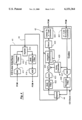
- FIG. 4 is a block diagram of the present codec 42 interfaced to a CO line interface 41.
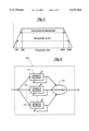
- FIG. 5 is a conceptual graph comparing the useable bandwidth available to a conventional subscriber modem, with the bandwidth available to the present codec at the central office.
- FIG. 6 is a block diagram of an array of adaptive equalizers 61-63 that can be used in place of a single equalizer 425 in the present codec.
- FIG. 7 is a block diagram of an alternative embodiment of the codec 42 using a four-wire interface to the CO line interface 41.
- FIG. 8 is a block diagram of the present codec 42 interfaced to a CO line interface 41 showing where these elements reside in a typical telephone network.
- FIG. 4 a schematic diagram is provided showing the present codec 42 connected to a central office line interface 41.
- FIG. 8 is a block diagram of the codec 42 interfaced to a CO line interface 41 showing where these elements reside in a typical telephone network.
- the CO line interface 41 is conventional in design, and is widely used to provide an analog or universal interface between a digital central office switch and an analog loop extending to the subscribers premises.
- a CO line interface 41 can also be used to interface the CO terminal of a DLC as shown in FIG. 2, or the CO terminal of a subscriber line multiplexer, as previously described with regard to FIG. 3.
- the CO line interface 41 receives pulse code modulated (PCM) signals from the CO switch that are converted to analog voltages by a digital-to-analog converter (DAC) 411.
- the analog signal passes through a reconstruction filter 412.
- a hybrid 413 is used to both send and receive analog signals over a single conventional pair of wires 43.
- the received analog signal is band-limited by an anti-aliasing filter 415.
- the filtered signals are sampled and converted into digital data by an analog-to-digital converter 414 (ADC), and output to the CO switch.
- ADC analog-to-digital converter 414
- the CO line interface 41 samples synchronously with the CO clock. This clock is used, for example, by both the DAC 411 and ADC 414.
- the codec 42 connects to the CO line interface 41 over the wire pair 43 by means of its hybrid 44. Downstream analog signals pass through an anti-aliasing filter 422 and are converted into digital signals by an analog-to-digital converter (ADC) 423.
- ADC analog-to-digital converter
- This ADC 423 is preferentially controlled by the same CO clock used by the CO line interface 41 to ensure that it has precisely the same sampling rate as the DAC 411 in the CO line interface 41. This is usually possible if the codec 42 is located adjacent to the CO line interface 41 by means of a common timing signal. In this case, the length of wire pair 43 connecting the CO line interface 41 and the codec 42 is typically only a few hundred feet, at most.
- the CO clock rate can be inferred by detecting periodic amplitude patterns in the analog signals received from the CO line interface 41.
- Methods for estimating the clock from the incoming analog signal in a multilevel PAM system are well understood in the art. Several methods may be employed, some of which are described by Proakis, Digital Communications, pages 358-365 (3 rd edition, McGraw Hill, Inc., 1995), which is hereby incorporated by reference.
- the output signal from the ADC 423 is then processed by at least one adaptive equalizer 425.
- the equalizer 425 has previously been trained to provide a transfer function that substantially compensates for distortions introduced by the reconstruction filter 412 and the signal path between the codec 42 and the reconstruction filter 412.
- the output of the adaptive equalizer 425 is sampled by a slicer 426 and converted into digital data.
- the slicer 426 is also synchronized to the CO clock to minimize resampling error.
- the digital data output by the slicer 426 undergoes conversion by a linear to ⁇ -law converter 424 ( ⁇ -law companding in North America and Japan, A-law companding elsewhere) to generate PCM codes for output over the DLC.
- This configuration allows the codec 42 to output a PCM stream that accurately reproduces the PCM codes entering the DAC 411 of the CO line interface 41.
- the equalizer must be initially trained prior to entering operational mode. This involves having a known training sequence sent through the channel and the equalizer 425, and comparing the equalizer output to the expected sequence.
- the equalizer filter taps are then adjusted based on an adaptive process such as the least-mean squares (LMS) algorithm to minimize error.
- LMS least-mean squares
- This algorithm is widely used in the telecommunications industry and is discussed by Widrow et al., Adaptive Signal Processing, Prentice Hall, Englewood Cliffs, N.J. (1985).
- the equalizer 425 taps are frozen for normal communications. Equalizer training can be repeated, as necessary, to compensate for changes in line conditions and the CO line interface 41.
- FIG. 6 illustrates an alternative embodiment in which a plurality of adaptive equalizers 61, 62, . . . 63 are arranged in parallel in place of the single equalizer 425 shown in FIG. 4.
- Each of the equalizers in the array 61-63 is trained to process one symbol in each frame of N symbols from the ADC 423. This approach is discussed in detail by Ayanoglu et al. in IEEE Transactions on Communications, supra, which is hereby incorporated by reference.
- upstream digital signals received by the codec 42 from the DLC pass through a ⁇ -law to linear converter 421, which linearizes the code space of the companded PCM received from the DLC.
- the linearized digital output from the ⁇ -law to linear converter 421 is converted into analog voltages by a digital-to-analog converter (DAC) 427.
- the resulting analog signal passes through a reconstruction filter 428 and is transmitted upstream to the CO line interface 41 over the wire pair 43 by the codec's hybrid 44.
- the upstream digital signal is also used by an echo canceller 429 to generate an echo estimate signal that is subtracted from the output of the ADC 423 to mitigate echo leaking through the hybrid 44.
- FIG. 7 is a schematic block diagram of an alternative embodiment of the present invention in which the two-wire interface 43 between CO line interface 41 and codec 42 has been replaced with an analog four-wire interface 431 and 432.
- One pair of wires 431 is used for downstream communications and the second pair 432 is used for upstream communications.
- This embodiment allows both of the hybrids 413 and 44 and the echo canceller 429 shown in FIG. 4 to be eliminated.
- the present codec could also be used in the CO line interface to facilitate the accurate reproduction of PCM codes in the upstream direction.
- this implementation could be used to enable PCM modem data transport in the upstream direction.
Abstract
Description
______________________________________
Inventor    Patent No.     Issue Date
______________________________________
Ayanoglu et al.
            5,394,437      Feb. 28, 1995
Ayanoglu et al.
            5,528,625      June 18, 1996
______________________________________
Claims (28)
Priority Applications (5)
| Application Number | Priority Date | Filing Date | Title |
|---|---|---|---|
| US09/183,709 US6151364A (en) | 1998-10-30 | 1998-10-30 | Codec supporting PCM modem communications over a universal digital loop carrier |
| US09/326,355 US6052412A (en) | 1998-10-30 | 1999-06-04 | Codec supporting PCM modem communications over a universal digital loop carrier |
| AU13252/00A AU1325200A (en) | 1998-10-30 | 1999-10-27 | Codec supporting pcm modem communications over a universal digital loop carrier |
| PCT/US1999/025170 WO2000027058A1 (en) | 1998-10-30 | 1999-10-27 | Codec supporting pcm modem communications over a universal digital loop carrier |
| TW088118898A TW437218B (en) | 1998-10-30 | 1999-10-30 | Codec supporting PCM modem communications over a universal digital loop carrier |
Applications Claiming Priority (1)
| Application Number | Priority Date | Filing Date | Title |
|---|---|---|---|
| US09/183,709 US6151364A (en) | 1998-10-30 | 1998-10-30 | Codec supporting PCM modem communications over a universal digital loop carrier |
Related Child Applications (1)
| Application Number | Title | Priority Date | Filing Date |
|---|---|---|---|
| US09/326,355 Continuation-In-Part US6052412A (en) | 1998-10-30 | 1999-06-04 | Codec supporting PCM modem communications over a universal digital loop carrier |
Publications (1)
| Publication Number | Publication Date |
|---|---|
| US6151364A true US6151364A (en) | 2000-11-21 |
Family
ID=22674004
Family Applications (1)
| Application Number | Title | Priority Date | Filing Date |
|---|---|---|---|
| US09/183,709 Expired - Fee Related US6151364A (en) | 1998-10-30 | 1998-10-30 | Codec supporting PCM modem communications over a universal digital loop carrier |
Country Status (1)
| Country | Link |
|---|---|
| US (1) | US6151364A (en) |
Cited By (25)
| Publication number | Priority date | Publication date | Assignee | Title |
|---|---|---|---|---|
| US6341360B1 (en) * | 1999-03-08 | 2002-01-22 | International Business Machines Corporation | Decision feedback equalizers, methods, and computer program products for detecting severe error events and preserving equalizer filter characteristics in response thereto |
| US6381267B1 (en) | 1999-03-08 | 2002-04-30 | International Business Machines Corporation | Modems, methods, and computer program products for falling back to a lower data rate protocol upon detecting abnormal line conditions during startup |
| US20020054630A1 (en) * | 2000-04-20 | 2002-05-09 | Gerald Hoefer | Method and apparatus for transformation of a signal |
| US6389064B1 (en) * | 1999-03-08 | 2002-05-14 | International Business Machines Corporation | Modems, methods, and computer program products for identifying a signaling alphabet in variance with an ideal alphabet due to digital impairments |
| US20020072879A1 (en) * | 1999-02-22 | 2002-06-13 | Sweitzer Steven R. | Method and apparatus for implementing digital filters in the data path of a PCM modem for efficient transition of a second analog-to-digital conversion process |
| US20020141428A1 (en) * | 2001-03-30 | 2002-10-03 | Posthuma Carl Robert | Line card and method for supporting a plurality of telecommunication services |
| US6480585B1 (en) * | 2001-02-15 | 2002-11-12 | Conexant Systems, Inc. | System and method for transmitting a facsimile via a network |
| US6487243B1 (en) | 1999-03-08 | 2002-11-26 | International Business Machines Corporation | Modems, methods, and computer program products for recovering from errors in a tone reversal sequence between two modems |
| US6516025B1 (en) * | 1999-04-29 | 2003-02-04 | Texas Instruments Incorporated | High-speed upstream modem communication |
| US6522688B1 (en) * | 1999-01-14 | 2003-02-18 | Eric Morgan Dowling | PCM codec and modem for 56K bi-directional transmission |
| US6553518B1 (en) | 1999-03-08 | 2003-04-22 | International Business Machines Corporation | Severe error detectors, methods and computer program products that use constellation specific error event thresholds to detect severe error events during demodulation of a signal comprising symbols from a plurality of symbol constellations |
| US6556638B1 (en) * | 1999-02-22 | 2003-04-29 | Godigital Networks Corporation | Method and apparatus for providing increased data speed using synchronization and bit robbing techniques |
| US6597732B1 (en) | 1999-01-14 | 2003-07-22 | Eric Morgan Dowling | High-speed modem with uplink remote-echo canceller |
| US6661847B1 (en) | 1999-05-20 | 2003-12-09 | International Business Machines Corporation | Systems methods and computer program products for generating and optimizing signal constellations |
| US6661837B1 (en) | 1999-03-08 | 2003-12-09 | International Business Machines Corporation | Modems, methods, and computer program products for selecting an optimum data rate using error signals representing the difference between the output of an equalizer and the output of a slicer or detector |
| US6697463B1 (en) | 1999-02-22 | 2004-02-24 | Godigital Networks Corporation | System for providing increased data speed using high resolution analog to digital conversion |
| US6754187B1 (en) * | 2000-04-06 | 2004-06-22 | Inter-Tel, Inc. | Performance enhancement system for digital PBX |
| US6885698B1 (en) | 2000-03-17 | 2005-04-26 | Godigital Networks Corporation | Efficient hardware implementation for signal reconstruction over multiple analog-to-digital, digital-to-analog conversions in a telecommunication system |
| US6967952B1 (en) | 2000-02-02 | 2005-11-22 | Godigital Networks, Corp. | Method and apparatus for providing high capacity, long loop broadband ADSL service |
| US7003030B2 (en) | 1999-03-08 | 2006-02-21 | Lenovo (Singapore) Pte. Ltd. | Receivers, methods, and computer program products for an analog modem that receives data signals from a digital modem |
| US7023911B1 (en) | 2000-03-17 | 2006-04-04 | Godigital Networks Corporation | Method and apparatus for altering a round trip delay measurement in a telecommunication system to accurately position an echo canceller |
| US7023877B1 (en) | 2001-10-31 | 2006-04-04 | Godigital Networks Corporation | Small form factor digital voice multiplexer with multiple DSL outputs |
| US7109906B1 (en) * | 2005-04-29 | 2006-09-19 | Freescale Semiconductor, Inc. | NICAM encoder featuring synchronization of a NICAM processor with front-end input and output sections |
| US20060244640A1 (en) * | 2005-04-29 | 2006-11-02 | Luciano Zoso | Front-end method for NICAM encoding |
| US10986164B2 (en) | 2004-01-13 | 2021-04-20 | May Patents Ltd. | Information device |
Citations (7)
| Publication number | Priority date | Publication date | Assignee | Title |
|---|---|---|---|---|
| US4646289A (en) * | 1984-06-29 | 1987-02-24 | Northern Telecom Limited | Signal multiplexing circuit |
| US5297163A (en) * | 1990-06-01 | 1994-03-22 | Schrack Telecom-Aktiengesellschaft | Method for processing signals for signal transmission in the base band |
| US5394437A (en) * | 1992-10-20 | 1995-02-28 | At&T Corp. | High-speed modem synchronized to a remote CODEC |
| US5528625A (en) * | 1994-01-03 | 1996-06-18 | At&T Corp. | High speed quantization-level-sampling modem with equalization arrangement |
| US5636244A (en) * | 1995-07-26 | 1997-06-03 | Motorola, Inc. | Method and apparatus for initializing equalizer coefficents using peridioc training sequences |
| US5801695A (en) * | 1994-12-09 | 1998-09-01 | Townshend; Brent | High speed communications system for analog subscriber connections |
| US5875229A (en) * | 1996-10-15 | 1999-02-23 | Motorola Inc. | System and device for, and method of, detecting, characterizing, and mitigating deterministic distortion in a communications network |
-
1998
- 1998-10-30 US US09/183,709 patent/US6151364A/en not_active Expired - Fee Related
Patent Citations (7)
| Publication number | Priority date | Publication date | Assignee | Title |
|---|---|---|---|---|
| US4646289A (en) * | 1984-06-29 | 1987-02-24 | Northern Telecom Limited | Signal multiplexing circuit |
| US5297163A (en) * | 1990-06-01 | 1994-03-22 | Schrack Telecom-Aktiengesellschaft | Method for processing signals for signal transmission in the base band |
| US5394437A (en) * | 1992-10-20 | 1995-02-28 | At&T Corp. | High-speed modem synchronized to a remote CODEC |
| US5528625A (en) * | 1994-01-03 | 1996-06-18 | At&T Corp. | High speed quantization-level-sampling modem with equalization arrangement |
| US5801695A (en) * | 1994-12-09 | 1998-09-01 | Townshend; Brent | High speed communications system for analog subscriber connections |
| US5636244A (en) * | 1995-07-26 | 1997-06-03 | Motorola, Inc. | Method and apparatus for initializing equalizer coefficents using peridioc training sequences |
| US5875229A (en) * | 1996-10-15 | 1999-02-23 | Motorola Inc. | System and device for, and method of, detecting, characterizing, and mitigating deterministic distortion in a communications network |
Non-Patent Citations (2)
| Title |
|---|
| Ender Ayanoglu et al., "An Equalizer Design Technique for the PCM Modem: A New Modem for the Digital Public Switched Network," IEEE Transactions on Communications, Jun. 1998, pp. 763-774, vol. 46, No. 6. |
| Ender Ayanoglu et al., An Equalizer Design Technique for the PCM Modem: A New Modem for the Digital Public Switched Network, IEEE Transactions on Communications, Jun. 1998, pp. 763 774, vol. 46, No. 6. * |
Cited By (33)
| Publication number | Priority date | Publication date | Assignee | Title |
|---|---|---|---|---|
| US7173962B2 (en) | 1999-01-14 | 2007-02-06 | Eric Morgan Dowling | High-speed modem with uplink remote-echo canceller |
| US6765967B2 (en) * | 1999-01-14 | 2004-07-20 | Eric Morgan Dowling | PCM codec and modem for 56k bi-directional transmission |
| US20040095994A1 (en) * | 1999-01-14 | 2004-05-20 | Dowling Eric Morgan | High-speed modem with uplink remote-echo canceller |
| US20030156632A1 (en) * | 1999-01-14 | 2003-08-21 | Dowling Eric Morgan | PCM codec and modem for 56k bi-directional transmission |
| US6597732B1 (en) | 1999-01-14 | 2003-07-22 | Eric Morgan Dowling | High-speed modem with uplink remote-echo canceller |
| US6522688B1 (en) * | 1999-01-14 | 2003-02-18 | Eric Morgan Dowling | PCM codec and modem for 56K bi-directional transmission |
| US6556638B1 (en) * | 1999-02-22 | 2003-04-29 | Godigital Networks Corporation | Method and apparatus for providing increased data speed using synchronization and bit robbing techniques |
| US7020189B2 (en) | 1999-02-22 | 2006-03-28 | Godigital Networks Corporation | Method and apparatus for implementing digital filters in the data path of a PCM modem for efficient transition of a second analog-to-digital conversion process |
| US20020072879A1 (en) * | 1999-02-22 | 2002-06-13 | Sweitzer Steven R. | Method and apparatus for implementing digital filters in the data path of a PCM modem for efficient transition of a second analog-to-digital conversion process |
| US6697463B1 (en) | 1999-02-22 | 2004-02-24 | Godigital Networks Corporation | System for providing increased data speed using high resolution analog to digital conversion |
| US7003030B2 (en) | 1999-03-08 | 2006-02-21 | Lenovo (Singapore) Pte. Ltd. | Receivers, methods, and computer program products for an analog modem that receives data signals from a digital modem |
| US6487243B1 (en) | 1999-03-08 | 2002-11-26 | International Business Machines Corporation | Modems, methods, and computer program products for recovering from errors in a tone reversal sequence between two modems |
| US6661837B1 (en) | 1999-03-08 | 2003-12-09 | International Business Machines Corporation | Modems, methods, and computer program products for selecting an optimum data rate using error signals representing the difference between the output of an equalizer and the output of a slicer or detector |
| US6381267B1 (en) | 1999-03-08 | 2002-04-30 | International Business Machines Corporation | Modems, methods, and computer program products for falling back to a lower data rate protocol upon detecting abnormal line conditions during startup |
| US6553518B1 (en) | 1999-03-08 | 2003-04-22 | International Business Machines Corporation | Severe error detectors, methods and computer program products that use constellation specific error event thresholds to detect severe error events during demodulation of a signal comprising symbols from a plurality of symbol constellations |
| US6341360B1 (en) * | 1999-03-08 | 2002-01-22 | International Business Machines Corporation | Decision feedback equalizers, methods, and computer program products for detecting severe error events and preserving equalizer filter characteristics in response thereto |
| US6389064B1 (en) * | 1999-03-08 | 2002-05-14 | International Business Machines Corporation | Modems, methods, and computer program products for identifying a signaling alphabet in variance with an ideal alphabet due to digital impairments |
| US6516025B1 (en) * | 1999-04-29 | 2003-02-04 | Texas Instruments Incorporated | High-speed upstream modem communication |
| US6661847B1 (en) | 1999-05-20 | 2003-12-09 | International Business Machines Corporation | Systems methods and computer program products for generating and optimizing signal constellations |
| US6967952B1 (en) | 2000-02-02 | 2005-11-22 | Godigital Networks, Corp. | Method and apparatus for providing high capacity, long loop broadband ADSL service |
| US20050281268A1 (en) * | 2000-02-02 | 2005-12-22 | Akers Francis I | Method and apparatus for providing high capacity, long loop broadband ADSL service |
| US7023911B1 (en) | 2000-03-17 | 2006-04-04 | Godigital Networks Corporation | Method and apparatus for altering a round trip delay measurement in a telecommunication system to accurately position an echo canceller |
| US6885698B1 (en) | 2000-03-17 | 2005-04-26 | Godigital Networks Corporation | Efficient hardware implementation for signal reconstruction over multiple analog-to-digital, digital-to-analog conversions in a telecommunication system |
| US6754187B1 (en) * | 2000-04-06 | 2004-06-22 | Inter-Tel, Inc. | Performance enhancement system for digital PBX |
| US20020054630A1 (en) * | 2000-04-20 | 2002-05-09 | Gerald Hoefer | Method and apparatus for transformation of a signal |
| US6836538B1 (en) | 2001-02-15 | 2004-12-28 | Mindspeed Technologies, Inc. | System and method for transmitting a facsimile via a network |
| US6480585B1 (en) * | 2001-02-15 | 2002-11-12 | Conexant Systems, Inc. | System and method for transmitting a facsimile via a network |
| US20020141428A1 (en) * | 2001-03-30 | 2002-10-03 | Posthuma Carl Robert | Line card and method for supporting a plurality of telecommunication services |
| US7023877B1 (en) | 2001-10-31 | 2006-04-04 | Godigital Networks Corporation | Small form factor digital voice multiplexer with multiple DSL outputs |
| US10986164B2 (en) | 2004-01-13 | 2021-04-20 | May Patents Ltd. | Information device |
| US7109906B1 (en) * | 2005-04-29 | 2006-09-19 | Freescale Semiconductor, Inc. | NICAM encoder featuring synchronization of a NICAM processor with front-end input and output sections |
| US20060244640A1 (en) * | 2005-04-29 | 2006-11-02 | Luciano Zoso | Front-end method for NICAM encoding |
| US7561076B2 (en) * | 2005-04-29 | 2009-07-14 | Freescale Semiconductor, Inc. | Front-end method for NICAM encoding |
Similar Documents
| Publication | Publication Date | Title |
|---|---|---|
| US6151364A (en) | Codec supporting PCM modem communications over a universal digital loop carrier | |
| US6052412A (en) | Codec supporting PCM modem communications over a universal digital loop carrier | |
| US5859872A (en) | High speed communications system for analog subscriber connections | |
| US6002713A (en) | PCM modem equalizer with adaptive compensation for robbed bit signalling | |
| JP2547844B2 (en) | Data communication method and communication network | |
| US6505222B1 (en) | Systems methods and computer program products for controlling undesirable bias in an equalizer | |
| JP4160097B2 (en) | High speed communication system for analog subscriber connection. | |
| US5970103A (en) | High speed communications system for analog subscriber connections | |
| US6792040B1 (en) | Modems having a dual power mode capability and methods of operating same | |
| US6556638B1 (en) | Method and apparatus for providing increased data speed using synchronization and bit robbing techniques | |
| WO2001058173A2 (en) | System and method for sampling phase adjustment by an analog modem | |
| US6233275B1 (en) | High speed communications system for analog subscriber connections | |
| US6823017B1 (en) | Systems, methods and computer program products for filtering glitches from measured values in a sequence of code points | |
| US6901107B1 (en) | Systems, methods, and computer program products for generating a digital impairment learning signal having low energy content at direct current and Nyquist frequencies | |
| US6754258B1 (en) | Systems, methods and computer program products for averaging learned levels in the presence of digital impairments based on patterns | |
| AU749051B2 (en) | A method of detecting the presence of robbed-bit signalling | |
| KR100349987B1 (en) | High speed communications system for analog subscriber connections | |
| AU749133B2 (en) | Methods for conveying information utilizing PCM codewords |
Legal Events
| Date | Code | Title | Description |
|---|---|---|---|
| AS | Assignment |
Owner name: RAYCHEM CORPORATION, CALIFORNIA Free format text: ASSIGNMENT OF ASSIGNORS INTEREST;ASSIGNORS:RUETHER, PETER GADE;FORD, CAROLYN GAYE;REEL/FRAME:009575/0391 Effective date: 19981030 |
|
| AS | Assignment |
Owner name: TYCO INTERNATIONAL LTD., A CORPORATION OF BERMUDA, Free format text: MERGER AND REORGANIZATION;ASSIGNOR:RAYCHEM CORPORATION, A CORPORATION OF DELAWARE;REEL/FRAME:010377/0665 Effective date: 19990812 Owner name: AMP INCORPORATED, A CORPORATION OF PENNSYLVANIA, P Free format text: MERGER AND REORGANIZATION;ASSIGNOR:RAYCHEM CORPORATION, A CORPORATION OF DELAWARE;REEL/FRAME:010377/0665 Effective date: 19990812 Owner name: TYCO ELECTRONICS CORPORATION, PENNSYLVANIA Free format text: CHANGE OF NAME;ASSIGNOR:AMP INCORPORATED;REEL/FRAME:010377/0684 Effective date: 19990913 Owner name: TYCO INTERNATIONAL (PA), INC., A CORPORATION OF NE Free format text: MERGER AND REORGANIZATION;ASSIGNOR:RAYCHEM CORPORATION, A CORPORATION OF DELAWARE;REEL/FRAME:010377/0665 Effective date: 19990812 |
|
| AS | Assignment |
Owner name: TERAYON COMMUNICATIONS SYSTEMS, INC., CALIFORNIA Free format text: ASSIGNMENT OF ASSIGNORS INTEREST;ASSIGNOR:TYCO ELECTRONICS CORPORATION;REEL/FRAME:011333/0447 Effective date: 20000414 |
|
| FEPP | Fee payment procedure |
Free format text: PAYOR NUMBER ASSIGNED (ORIGINAL EVENT CODE: ASPN); ENTITY STATUS OF PATENT OWNER: LARGE ENTITY |
|
| REMI | Maintenance fee reminder mailed | ||
| LAPS | Lapse for failure to pay maintenance fees | ||
| LAPS | Lapse for failure to pay maintenance fees |
Free format text: PATENT EXPIRED FOR FAILURE TO PAY MAINTENANCE FEES (ORIGINAL EVENT CODE: EXP.); ENTITY STATUS OF PATENT OWNER: LARGE ENTITY |
|
| STCH | Information on status: patent discontinuation |
Free format text: PATENT EXPIRED DUE TO NONPAYMENT OF MAINTENANCE FEES UNDER 37 CFR 1.362 |
|
| FP | Lapsed due to failure to pay maintenance fee |
Effective date: 20041121 |