US6151435A - Evanescent atom guiding in metal-coated hollow-core optical fibers - Google Patents
Evanescent atom guiding in metal-coated hollow-core optical fibers Download PDFInfo
- Publication number
- US6151435A US6151435A US09/184,208 US18420898A US6151435A US 6151435 A US6151435 A US 6151435A US 18420898 A US18420898 A US 18420898A US 6151435 A US6151435 A US 6151435A
- Authority
- US
- United States
- Prior art keywords
- atom
- optical fiber
- hollow
- fiber
- guiding
- Prior art date
- Legal status (The legal status is an assumption and is not a legal conclusion. Google has not performed a legal analysis and makes no representation as to the accuracy of the status listed.)
- Expired - Fee Related
Links
- 239000013307 optical fiber Substances 0.000 title claims abstract description 23
- 229910052751 metal Inorganic materials 0.000 title claims abstract description 15
- 239000002184 metal Substances 0.000 title claims abstract description 15
- 239000000835 fiber Substances 0.000 claims abstract description 19
- 239000011248 coating agent Substances 0.000 claims abstract description 6
- 238000000576 coating method Methods 0.000 claims abstract description 6
- VYZAMTAEIAYCRO-UHFFFAOYSA-N Chromium Chemical compound [Cr] VYZAMTAEIAYCRO-UHFFFAOYSA-N 0.000 claims description 2
- BQCADISMDOOEFD-UHFFFAOYSA-N Silver Chemical compound [Ag] BQCADISMDOOEFD-UHFFFAOYSA-N 0.000 claims description 2
- 229910052782 aluminium Inorganic materials 0.000 claims description 2
- XAGFODPZIPBFFR-UHFFFAOYSA-N aluminium Chemical compound [Al] XAGFODPZIPBFFR-UHFFFAOYSA-N 0.000 claims description 2
- 229910052804 chromium Inorganic materials 0.000 claims description 2
- 239000011651 chromium Substances 0.000 claims description 2
- 238000004891 communication Methods 0.000 claims description 2
- PCHJSUWPFVWCPO-UHFFFAOYSA-N gold Chemical compound [Au] PCHJSUWPFVWCPO-UHFFFAOYSA-N 0.000 claims description 2
- 229910052737 gold Inorganic materials 0.000 claims description 2
- 239000010931 gold Substances 0.000 claims description 2
- 229910052709 silver Inorganic materials 0.000 claims description 2
- 239000004332 silver Substances 0.000 claims description 2
- PXHVJJICTQNCMI-UHFFFAOYSA-N Nickel Chemical compound [Ni] PXHVJJICTQNCMI-UHFFFAOYSA-N 0.000 claims 2
- 150000002739 metals Chemical class 0.000 claims 1
- 229910052759 nickel Inorganic materials 0.000 claims 1
- 230000004888 barrier function Effects 0.000 abstract description 20
- 230000005641 tunneling Effects 0.000 abstract description 9
- 238000005076 Van der Waals potential Methods 0.000 abstract description 3
- 238000005452 bending Methods 0.000 abstract description 3
- 230000000694 effects Effects 0.000 abstract description 3
- 230000005684 electric field Effects 0.000 description 9
- 230000001427 coherent effect Effects 0.000 description 5
- 230000003993 interaction Effects 0.000 description 3
- 230000007704 transition Effects 0.000 description 3
- 239000004020 conductor Substances 0.000 description 2
- 239000012510 hollow fiber Substances 0.000 description 2
- 238000000034 method Methods 0.000 description 2
- 229910052770 Uranium Inorganic materials 0.000 description 1
- 238000004458 analytical method Methods 0.000 description 1
- 238000004364 calculation method Methods 0.000 description 1
- 238000005253 cladding Methods 0.000 description 1
- 230000007717 exclusion Effects 0.000 description 1
- 238000001307 laser spectroscopy Methods 0.000 description 1
- 239000000463 material Substances 0.000 description 1
- 238000007620 mathematical function Methods 0.000 description 1
- 230000007935 neutral effect Effects 0.000 description 1
- 238000001579 optical reflectometry Methods 0.000 description 1
- IGLNJRXAVVLDKE-UHFFFAOYSA-N rubidium atom Chemical group [Rb] IGLNJRXAVVLDKE-UHFFFAOYSA-N 0.000 description 1
Images

Classifications
-
- G—PHYSICS
- G21—NUCLEAR PHYSICS; NUCLEAR ENGINEERING
- G21K—TECHNIQUES FOR HANDLING PARTICLES OR IONISING RADIATION NOT OTHERWISE PROVIDED FOR; IRRADIATION DEVICES; GAMMA RAY OR X-RAY MICROSCOPES
- G21K1/00—Arrangements for handling particles or ionising radiation, e.g. focusing or moderating
- G21K1/06—Arrangements for handling particles or ionising radiation, e.g. focusing or moderating using diffraction, refraction or reflection, e.g. monochromators
-
- H—ELECTRICITY
- H05—ELECTRIC TECHNIQUES NOT OTHERWISE PROVIDED FOR
- H05H—PLASMA TECHNIQUE; PRODUCTION OF ACCELERATED ELECTRICALLY-CHARGED PARTICLES OR OF NEUTRONS; PRODUCTION OR ACCELERATION OF NEUTRAL MOLECULAR OR ATOMIC BEAMS
- H05H3/00—Production or acceleration of neutral particle beams, e.g. molecular or atomic beams
- H05H3/04—Acceleration by electromagnetic wave pressure
Abstract
A new type of atom guiding structure has been analyzed. It consists of a low-core optical fiber (step-index) which is not clad, but instead has a metal coating on its outer lateral surface. It will be shown that this structure produces the maximum evanescent field in the hollow region of the fiber and guiding can be accomplished with lower power lasers. Both the dipole and the vander Waals potentials have been combined and the resulting barrier height was maximized as a function of both Δ, the detuning, and r, the position. An optimized potential having a barrier height of 1 K has been determined by iteratively solving for the required laser intensity. The probability of atoms tunneling through this barrier to the inner wall has been calculated and is expected to be unimportant. Centripetal effects due to a bending of the fiber have also been estimated and are small for the barrier considered here. Compared to other structures, this new-type of guide provides bigger barriers for the same laser power, and therefore enhanced atom guiding.
Description
1. Technical Field
The invention relates generally to a method and apparatus for guiding atoms by blue-detuned evanescent waves in a hollow-core optical fiber. More particularly, the invention relates to the use of a metal-coated hollow-core optical fiber as the wave guide to maximize the evanescent guiding field in the hollow region of the fiber.
2. Background Art
The polarizability of an atom is almost always positive, but it can be negative and some unusual effects can then be observed. This can occur when a laser or other monochromatic source is tuned slightly above or to the "blue" of an atomic resonance. The interaction of the external field on the atom through its negative polarizability produces a gradient dipole force which tends to drive the atom to regions of minimum intensity. Cook and Hill suggested using an evanescent wave to produce an atom mirror outside of a dielectric. Reference: R. J. Cook, R. K. Hill, An Electromagnetic Mirror for Neutral Atoms, Optics Comm. 43 (1982) 258. Zoller, et. al. analyzed the case for a clad, hollow fiber in which the external field was confined to the annular region and used the resulting evanescent field in the hollow region to guide atoms. Reference: S. Marksteiner, C. M. Savage, P. Zoller, S. L. Rolston, Coherent Atomic Waveguides from Hollow Optical Fibers: Quantized Atomic Motion, Phys. Rev. A 50 (1994) 2680. In what has become known as "blue-guiding", Renn and Ito have experimentally demonstrated evanescent wave guiding of rubidium atoms in hollow optical fibers. See: M. J. Renn, E. A. Donley, E. A. Cornell, C. E. Wiemann, D. Z. Anderson, Evanscent-wave Guiding of Atoms in Hollow Optical Fibers, Phys. Rev. A 53 (1996) 648A; and H. Ito, T. Nakata, K. Sakaki, M. Ohtsu, K. I. Lee, W. Jhe, Laser Spectroscopy of Atoms Guided by Evanscent Waves in Micron-sized Hollow Optical Fibers, Phys. Rev. Lett. 76 (1996) 4500.
It is an object of the invention to provide an improved method for guiding atoms by evanescent laser light through hollow-core optical fibers, which maximizes the evanescent guiding field in the hollow region of the fiber.
It is another object of the invention to provide a new type of atom guiding structure which can be used in existing systems for guiding atoms through hollow-core optical fibers, which maximizes the guiding barrier for a given laser power.
It is a further object of the invention to provide such a new type of atom guiding structure which also minimizes the loss of atoms to the inner wall of the fiber from quantum tunneling.
It is still another object of the invention to provide such a new type of atom guiding structure which also minimizes the loss of atoms to the inner wall of the fiber from centripetal force due to physical bending of the fiber.
The atom guiding structure, according to the invention, comprises a hollow-core optical fiber (step index) which has a coating on its outer lateral surface of a material, such as a metal, which has a high optical reflectivity. Typically, this coating comprises a metal having very high electrical conductivity, such as silver, gold, chromium, and aluminum.
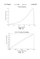
FIG. 1. shows the longitudinal electric fields, Ez2, of the five lowest-order TM modes, TM01 . . . TM05, of the metal-coated hollow dielectric cylindrical atom guide analyzed herein, between the inner radius a, and the outer radius, b of the cylinder, normalized to 1 V/m at r=a, indicating that, for each mode, Ez2 has a maximum at r=a.
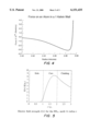
FIG. 2. shows the 1 K barrier an atom must tunnel through in order to reach the inner wall.
FIG. 3. shows the probability per bounce of tunneling through a 1 K barrier as a fraction of the initial energy.
FIG. 4. shows the force on an atom in a 1 Kelvin Well.
FIG. 5. shows the electric field strength, Ez, for the HE11 mode vs the radius r for a clad hollow-core optical fiber (Reference: S. Marksteiner, C. M. Savage, P. Zoller, S. L.Rolston, Phys. Rev. A 50 (1994) 2680, cited above.).
A new type of enhanced, atom guiding structure has been analyzed. It consists of a hollow-core, step index optical fiber which is not clad but instead has a metal coating on its outer lateral surface. It will be shown that the longitudinal electric fields of the lowest order TMOn modes of this structure have a global maximum at the inner wall of the hollow fiber. This produces the maximum barrier and therefore, maximum guiding in the hollow region of the fiber.
A perfect, hollow dielectric cylinder of inner radius, a, outer radius, b, and longitudinal axis in the z direction, is analyzed as an atom guide. The outer lateral surface at radius, b, is assumed to be coated with a perfect conductor, This coating not only produces a structure having significant advantages as an atom guide but also greatly simplifies the boundary conditions. The lowest order TM modes of this infinitely long wave guide are calculated in the standard way, which is set forth in the textbook Fields and Waves in Communication Electronics, Third Edition,(Wiley, N.Y., 1993), which is incorporated herein by reference. The Helmholtz equation for Ez1 in the hollow region (r≦a) is given by: ##EQU1## where
w.sub.1.sup.2 =(β.sup.2 -k.sup.2) a.sup.2 >0, (2)
and Ez2 in the annular dielectric (a≦,r≦b) is ##EQU2## where
u.sub.2.sup.2 =(k.sub.2.sup.2 -β.sup.2)a.sup.2 >0. (4)
Here w1 and u2 are the eigenvalues of equations (1) and (3), respectively, β is the propagation constant in the z direction, k=2π/λ is the wave number (free space) where λ is the wavelength, and k2 =n2 k is the wave number in the dielectric of index of refraction n2. For zero azimuthal dependence, the general solution of equation (1) is ##EQU3## and for equation (3) is ##EQU4## where J.sub.ν, Y.sub.ν, I.sub.ν, and K.sub.ν, are Bessel functions of order ν, as set forth in the Handbook of Mathematical Functions, M. Abramowitz and I. Stegun, Editors, (Dover, N.Y., 1965) pages 355-430, incorporated herein by reference. A, B, C, and D are constants determined by the boundary conditions. The zero azimuthal dependence automatically permits the exclusion of hybrid modes as the solutions separate into TM and TE sets.
Equations (5 and 6) are solved simultaneously subject to the following boundary conditions: Ez1 (r=0) is finite, Ez1 (r=a)=Ez2 (r=a)=1 (normalizes solutions to unity), Ez2 (r=b)=0, and H.sub.φ1 (r=a)=H.sub.φ2 (r=a). The solution of these equations gives the first of the two determinental equations, which for zero azimuthal dependence, reduces to ##EQU5## where .di-elect cons.1 =.di-elect cons.0, the vacuum permittivity, and .di-elect cons.2 =n2 2 .di-elect cons.0. For the case to be considered here where b=3a, this reduces to ##EQU6## The second determinental equation is obtained from (2) and (4) as
u.sub.2.sup.2 +w.sub.1.sup.2 =a.sup.2 k.sup.2 (n.sub.2.sup.2 -1).(9)
Equations (8) and (9) can be solved either graphically or numerically for the eigenvalues, w1 or u2. For the parameters of the guide described here: a=2.5 μm, λ=0.5 μm, and n2 =√5, the results for the five lowest-order TM modes (TM01 . . . TM05) have been calculated and the corresponding eigenvectors Ez2 are shown in FIG. 1. It is significant that all of the Ez2 shown here have their global maximum value at r=a. This gives the maximum possible values for the evanescent fields, Er1 at r=a, because the fields in the hollow region have unique solutions which do not depend on the solutions in the annular region except in so far as they are connected by the boundary conditions at the interface (r=a).
The potential ener for the interaction of an atomic dipole in an oscillating electric field is treated classically as ##EQU7## where α is the polarizability. In the hollow part of the guide, E is the evanescent field Er1, and neglecting the phase factor, ##EQU8## where, for the guide considered here, β=2.81×10⁷ m-1, w1 =62.8, u2 =0.960, and EL is the laser field strength in the dielectric at the interface r=a. The required laser intensity, IL, is given by IL =1/2n2 .di-elect cons.0 c EL 2. While the classical description of the dipole potential provides a simple understanding of the geometric aspects of this interaction because the induced dipole moment is co-linear with the evanescent field and this field must be in the radial direction in order to guide atoms, the quantum representation is necessary in order to analyze this problem in more detail. The quantum dipole potential, Udip-qm, is given by ##EQU9## where h=h/2π=1.05×10-34 J·s, the detuning Δ=ω-ω0, γ is the decay rate of the upper level, d is the transition dipole moment between levels 1 and 2, and E is the electric field amplitude given by equation (10). See: A. Ashkin, Phys. Rev. Lett. 40 (1978) 729; and J. Dalibard and C. Cohen-Tannoudji, J. Opt. Soc. Am. B 2 (1985) 1707. The van der Waals potential for an atom in proximity to an infinite dielectric slab is given by ##EQU10## where .di-elect cons. is the dielectric constant, μ2.sub.Σ is the sum of the squares of all the transition dipole moments, and x is the distance from the atom to the dielectric surface. See: M. J. Renn, E. A. Donley, E. A. Cornell, C. E. Wiemann, D. Z. Anderson, Evanscent-wave Guiding of Atoms in Hollow Optical Fibers, Phys. Rev. A 53 (1996) 648A, cited above. This represents an approximation of the attractive potential tending to draw the atom to the inner wall of the cylinder, Changing variables from x to r, the distance from the center of the cylinder, substituting .di-elect cons.=n2 2, and adding a constant offset term to make Uvdw =0 at r=0 gives ##EQU11##
The total potential, U, in the hollow region is obtained by adding (11 and 12) where ##EQU12## A synthetic two level atom has been assumed for Udip-qm with the following properties: d=2.10×10⁻²⁹ Cm and γ=108 s-1. For Uvdw, a multilevel atom was assumed where μ2.sub.Σ =9×10-58 C2 m2 and is equivalent to a two-level atom whose transition dipole moment is 1.50×d. Substituting these values together with the solution for the TM01 mode into (13) gives ##EQU13## Equation (14) was simultaneously maximized in both r and Δ. For EL =2.68×10⁶ V/m (corresponding to a laser input intensity of 2.13×10⁶ w/cm2), Umax, the maximum value for U, was found to be 1.00 K for Δ=1.76×10¹¹ s-1 and r=2.4925 μm. The 1 Kelvin barrier is shown in FIG. 2. This barrier is representative of conditions for which the loss of atoms via tunneling to the inner wall of the fiber is of interest. Near the inner wall, the van der Waals potential is strongly attractive and dominates the total potential there. The tunneling can be calculated using the WKB approximation, described in Quantum Theory, by D. Bohm (Prentice-Hall, N.Y., 1951) and in textbfQuantum Mechanics, by D. H. Rapp (Holt, Rinehart and Winston, N.Y., 1971), which yields ##EQU14## where T is the tunneling probability per bounce, tp1 and tp2 are the turning points for the initial energy, m is the mass of the atom and is taken here to be 4.00×10⁻²⁶ kg, U is given by equation(14), ƒ is the fraction of the total barrier height corresponding to the initial energy. This is at least a useful approximation as the tunneling is small in the region of interest, ƒ≦0.98, and the de Broglie wavelength, λdB =0.901 nm for (ƒ=0.98), is small compared to the minimum thickness, (tp2 -tp1)≧3.58 nm, of the barrier in this region. The probability per bounce for an atom to tunnel through a 1 K barrier to the wall is shown in FIG. 3 where the fraction of initial energy ranges from 0.80 to 1.00 of the barrier height. For this barrier, the probability of tunneling per bounce is T≦10-3 for ƒ≦0.98 of the total barrier height. From FIG. 3, it can be seen that for ƒ≈0.90, quantum tunneling is expected to be unimportant.
A curved or bent fiber will generate a centripetal force on the atom as it moves in an arc around the bend. If this force is greater than the inward repulsive force of the potential, then the atom will penetrate the barrier, hit the wall, and be lost. For the 1 K barrier considered above, the force (which includes both the dipole and the van der Wall forces) is shown in FIG. 4. An estimate of the minimum bending radius, ##EQU15## is derived in a publication by J. P. Dowling and J. Gea-Banaeloche, Adv. At. Mol. Opt. Phys. 36 (1996) 1, and has been calculated in two references cited above, namely, S. Marksteiner, C. M. Savage, P. Zoller, S. L. Rolston, Coherent Atomic Waveguides from Hollow Optical Fibers: Quantized Atomic Motion, Phys. Rev. A 50 (1994) 2680; and M. J. Renn, E. A. Donley, E. A. Cornell, C. E. Wiemann, D. Z. Anderson, Evanscent-wave Guiding of Atoms in Hollow Optical Fibers, Phys. Rev. A 53 (1996) 648. Here a is the radius of the fiber, v.sub.|| is the longitudinal velocity, and v.sub.⊥ is the maximum allowed trapped transverse velocity. For a 1 K barrier and a longitudinal velocity of the beam appropriate to 1000 K, Rmin =0.5 cm., and centripetal effects are small for the potential used here.
Zoller, et. al. have reported a comprehensive analysis of evanescent blue-guiding of atoms. Refer to: S. Marksteiner, C. M. Savage, P. Zoller, S. L. Rolston, "Coherent Atomic Waveguides from Hollow Optical Fibers: Quantized Atomic Motion", Phys. Rev. A 50 (1994) 2680, cited above and incorporated herein by reference. They analyzed a clad, hollow dielectric fiber and primarily considered the hybrid HE11 mode because they were mainly interested in a single mode fiber. The enhancement provided by the metal-coated fiber can be estimated by comparing the guiding produced by the HE11 mode in their clad fiber with that in a TM01 mode in an identical fiber except that the cladding has been removed and the outer dielectric surface is coated with a perfect conductor which is a perfect reflector. The radial dependence of the longitudinal electric field, Ez from the above-cited reference (S. Maxksteiner, C. M. Savage, P. Zoller, S. L. Rolston, "Coherent Atomic Waveguides from Hollow Optical Fibers: Quantized Atomic Motion", Phys. Rev. A 50 (1994) 2680) is shown with permission in FIG. 5. It is seen that the maximum electric field occurs well inside the core and is about 81/2 times larger than the field at the hole-core boundary (r/ρ1 =1) where ρ1 =a in their notation. (As expected, a calculation using their parameters (a=1.65 μm, b=3.3 μm, n2 =1.5, and λ=0.57 μm) for the TM01 mode shows that the maximum value of Ez occurs at (r=a)). The radial electric fields in the hollow region have been calculated for the TM01 and HE11 modes as Er1TM and Er1HE, respectively. For the case where Ez2TM (r=a)=Ez2HE (r=a), Er1TM and EEr1HE appear to be identical. An amplitude scaling factor is defined as S=[Ez2 (r=a)/Ez2 (max)] and STM01 =1.00 (FIG. 1) and SHE11 =˜(81/2)-1 (FIG. 5). From the boundary conditions, Ez1 (r=a)=Ez2 (r=a) and Hz1 (r=a)=Hz2 (r=a), it can be shown that Er1 scales directly with S. The ratio of the radial electric fields can be written as [Er1TM (r=a)/Er1HE (r=a)]=STM01 /SHE11 =˜81/2. Because the dipole potential, equation (13), depends on E2 r1 in a somewhat complicated way.1, and the enhanced guiding is due to the fact that one mode is more effective than another in producing a larger Er1 (r=a) for the same maximum value of Ez2, the enhancement will be calculated in terms of the increased laser intensity required to satisfy the condition: Er1HE (r=a)=Er1TM (r=a). The result is that the laser intensity must be increased by the factor [STM01 /SHE11 ]2 =˜(81/2)2 ˜72 in order for the dielectric-clad fiber to provide the same degree of guiding as in the metal-coated fiber.
The use of the TM01 mode in the metal-coated guide proposed here offers several advantages over structures considered previously. First, Ez2 has a global maximum at r=a and provides for maximum guiding in the hollow region. While FIG. 1 shows that the lowest five modes have a global maximum at r=a, it has not been proven that this is the case for all of the allowed TM0n modes. These modes are expected to be partially coherent and their travelling waves will average over the relatively slow motion of the atoms, and should only result in a modest correction to the effective laser field in the expression for Udip-qm.
The use of the metal coated "atom guide" described herein will enhance the performance of, as well as permit the minaturization of devices such as atomic clocks, and atom interfer-ometers and their applications such as rotational and gravitational sensors.
Claims (2)
1. An atom guiding apparatus which comprises:
a first vacuum chamber;
a second vacuum chamber;
a metal-coated hollow-core optical fiber extending between the first and second vacuum chambers, having a first open end extending into the first vacuum chamber and having a second opposite open end extending into the second vacuum chamber whereby the first chamber is in communication with the second chamber through the hollow-core portion of the optical fiber, the optical fiber having an annular dielectric portion with concentric inner and outer surfaces, the dielectric inner surface extending about and defining the hollow core of the optical fiber, and the dielectric outer surface being metal-coated;
atom supply means for supplying identical atoms into the first chamber;
atom directing means for directing at least some of the identical atoms toward and into the first open end of the optical fiber;
a tunable monochromatic light source, which is tuned slightly above the resonance of said atoms in the first vacuum chamber, and
light directing means for directing the monchromatic light into one end of the annular dielectric portion of the fiber,the monochromatic light traversing the length of the optical fiber and producing a maximum evanescent field in the hollow portion of the optical fiber.
2. An atom guiding apparatus, as described in claim 1, wherein the metal coating comprises at least one of the following metals: gold, silver, chromium, nickel, and aluminum.
Priority Applications (1)
| Application Number | Priority Date | Filing Date | Title |
|---|---|---|---|
| US09/184,208 US6151435A (en) | 1998-11-01 | 1998-11-01 | Evanescent atom guiding in metal-coated hollow-core optical fibers |
Applications Claiming Priority (1)
| Application Number | Priority Date | Filing Date | Title |
|---|---|---|---|
| US09/184,208 US6151435A (en) | 1998-11-01 | 1998-11-01 | Evanescent atom guiding in metal-coated hollow-core optical fibers |
Publications (1)
| Publication Number | Publication Date |
|---|---|
| US6151435A true US6151435A (en) | 2000-11-21 |
Family
ID=22675984
Family Applications (1)
| Application Number | Title | Priority Date | Filing Date |
|---|---|---|---|
| US09/184,208 Expired - Fee Related US6151435A (en) | 1998-11-01 | 1998-11-01 | Evanescent atom guiding in metal-coated hollow-core optical fibers |
Country Status (1)
| Country | Link |
|---|---|
| US (1) | US6151435A (en) |
Cited By (18)
| Publication number | Priority date | Publication date | Assignee | Title |
|---|---|---|---|---|
| US20030020768A1 (en) * | 1998-09-30 | 2003-01-30 | Renn Michael J. | Direct write TM system |
| US20030048314A1 (en) * | 1998-09-30 | 2003-03-13 | Optomec Design Company | Direct write TM system |
| US20030228124A1 (en) * | 1998-09-30 | 2003-12-11 | Renn Michael J. | Apparatuses and method for maskless mesoscale material deposition |
| US20040179808A1 (en) * | 1998-09-30 | 2004-09-16 | Optomec Design Company | Particle guidance system |
| US20040197493A1 (en) * | 1998-09-30 | 2004-10-07 | Optomec Design Company | Apparatus, methods and precision spray processes for direct write and maskless mesoscale material deposition |
| US6823124B1 (en) * | 1998-09-30 | 2004-11-23 | Optomec Design Company | Laser-guided manipulation of non-atomic particles |
| US7294366B2 (en) | 1998-09-30 | 2007-11-13 | Optomec Design Company | Laser processing for heat-sensitive mesoscale deposition |
| US7674671B2 (en) | 2004-12-13 | 2010-03-09 | Optomec Design Company | Aerodynamic jetting of aerosolized fluids for fabrication of passive structures |
| US7938341B2 (en) | 2004-12-13 | 2011-05-10 | Optomec Design Company | Miniature aerosol jet and aerosol jet array |
| US7938079B2 (en) | 1998-09-30 | 2011-05-10 | Optomec Design Company | Annular aerosol jet deposition using an extended nozzle |
| US8110247B2 (en) | 1998-09-30 | 2012-02-07 | Optomec Design Company | Laser processing for heat-sensitive mesoscale deposition of oxygen-sensitive materials |
| US8272579B2 (en) | 2007-08-30 | 2012-09-25 | Optomec, Inc. | Mechanically integrated and closely coupled print head and mist source |
| CN103217804A (en) * | 2013-04-28 | 2013-07-24 | 中国科学院上海光学精密机械研究所 | Device for generating one-dimensional single-color dislocated rubidium-strontium optical lattice |
| US8887658B2 (en) | 2007-10-09 | 2014-11-18 | Optomec, Inc. | Multiple sheath multiple capillary aerosol jet |
| US9192054B2 (en) | 2007-08-31 | 2015-11-17 | Optomec, Inc. | Apparatus for anisotropic focusing |
| CN105783902A (en) * | 2016-05-10 | 2016-07-20 | 北京航天控制仪器研究所 | Angular speed measuring method based on hollow metal optical fiber atomic guidance |
| US10632746B2 (en) | 2017-11-13 | 2020-04-28 | Optomec, Inc. | Shuttering of aerosol streams |
| US10994473B2 (en) | 2015-02-10 | 2021-05-04 | Optomec, Inc. | Fabrication of three dimensional structures by in-flight curing of aerosols |
Citations (1)
| Publication number | Priority date | Publication date | Assignee | Title |
|---|---|---|---|---|
| US5528028A (en) * | 1990-06-01 | 1996-06-18 | Chu; Steven | Frequency standard using an atomic stream of optically cooled atoms |
-
1998
- 1998-11-01 US US09/184,208 patent/US6151435A/en not_active Expired - Fee Related
Patent Citations (1)
| Publication number | Priority date | Publication date | Assignee | Title |
|---|---|---|---|---|
| US5528028A (en) * | 1990-06-01 | 1996-06-18 | Chu; Steven | Frequency standard using an atomic stream of optically cooled atoms |
Cited By (33)
| Publication number | Priority date | Publication date | Assignee | Title |
|---|---|---|---|---|
| US7987813B2 (en) | 1998-09-30 | 2011-08-02 | Optomec, Inc. | Apparatuses and methods for maskless mesoscale material deposition |
| US7045015B2 (en) | 1998-09-30 | 2006-05-16 | Optomec Design Company | Apparatuses and method for maskless mesoscale material deposition |
| US20030228124A1 (en) * | 1998-09-30 | 2003-12-11 | Renn Michael J. | Apparatuses and method for maskless mesoscale material deposition |
| US20030020768A1 (en) * | 1998-09-30 | 2003-01-30 | Renn Michael J. | Direct write TM system |
| US20040197493A1 (en) * | 1998-09-30 | 2004-10-07 | Optomec Design Company | Apparatus, methods and precision spray processes for direct write and maskless mesoscale material deposition |
| US6823124B1 (en) * | 1998-09-30 | 2004-11-23 | Optomec Design Company | Laser-guided manipulation of non-atomic particles |
| US20050163917A1 (en) * | 1998-09-30 | 2005-07-28 | Optomec Design Company | Direct writeTM system |
| US8110247B2 (en) | 1998-09-30 | 2012-02-07 | Optomec Design Company | Laser processing for heat-sensitive mesoscale deposition of oxygen-sensitive materials |
| US7108894B2 (en) | 1998-09-30 | 2006-09-19 | Optomec Design Company | Direct Write™ System |
| US7270844B2 (en) | 1998-09-30 | 2007-09-18 | Optomec Design Company | Direct write™ system |
| US7294366B2 (en) | 1998-09-30 | 2007-11-13 | Optomec Design Company | Laser processing for heat-sensitive mesoscale deposition |
| US7485345B2 (en) | 1998-09-30 | 2009-02-03 | Optomec Design Company | Apparatuses and methods for maskless mesoscale material deposition |
| US7658163B2 (en) | 1998-09-30 | 2010-02-09 | Optomec Design Company | Direct write# system |
| US8455051B2 (en) | 1998-09-30 | 2013-06-04 | Optomec, Inc. | Apparatuses and methods for maskless mesoscale material deposition |
| US20030048314A1 (en) * | 1998-09-30 | 2003-03-13 | Optomec Design Company | Direct write TM system |
| US7938079B2 (en) | 1998-09-30 | 2011-05-10 | Optomec Design Company | Annular aerosol jet deposition using an extended nozzle |
| US20040179808A1 (en) * | 1998-09-30 | 2004-09-16 | Optomec Design Company | Particle guidance system |
| US9607889B2 (en) | 2004-12-13 | 2017-03-28 | Optomec, Inc. | Forming structures using aerosol jet® deposition |
| US7674671B2 (en) | 2004-12-13 | 2010-03-09 | Optomec Design Company | Aerodynamic jetting of aerosolized fluids for fabrication of passive structures |
| US7938341B2 (en) | 2004-12-13 | 2011-05-10 | Optomec Design Company | Miniature aerosol jet and aerosol jet array |
| US8796146B2 (en) | 2004-12-13 | 2014-08-05 | Optomec, Inc. | Aerodynamic jetting of blended aerosolized materials |
| US8132744B2 (en) | 2004-12-13 | 2012-03-13 | Optomec, Inc. | Miniature aerosol jet and aerosol jet array |
| US8640975B2 (en) | 2004-12-13 | 2014-02-04 | Optomec, Inc. | Miniature aerosol jet and aerosol jet array |
| US9114409B2 (en) | 2007-08-30 | 2015-08-25 | Optomec, Inc. | Mechanically integrated and closely coupled print head and mist source |
| US8272579B2 (en) | 2007-08-30 | 2012-09-25 | Optomec, Inc. | Mechanically integrated and closely coupled print head and mist source |
| US9192054B2 (en) | 2007-08-31 | 2015-11-17 | Optomec, Inc. | Apparatus for anisotropic focusing |
| US8887658B2 (en) | 2007-10-09 | 2014-11-18 | Optomec, Inc. | Multiple sheath multiple capillary aerosol jet |
| CN103217804A (en) * | 2013-04-28 | 2013-07-24 | 中国科学院上海光学精密机械研究所 | Device for generating one-dimensional single-color dislocated rubidium-strontium optical lattice |
| CN103217804B (en) * | 2013-04-28 | 2015-08-12 | 中国科学院上海光学精密机械研究所 | Produce the device of one-dimensional single-color dislocation rubidium strontium optical lattice |
| US10994473B2 (en) | 2015-02-10 | 2021-05-04 | Optomec, Inc. | Fabrication of three dimensional structures by in-flight curing of aerosols |
| CN105783902A (en) * | 2016-05-10 | 2016-07-20 | 北京航天控制仪器研究所 | Angular speed measuring method based on hollow metal optical fiber atomic guidance |
| US10632746B2 (en) | 2017-11-13 | 2020-04-28 | Optomec, Inc. | Shuttering of aerosol streams |
| US10850510B2 (en) | 2017-11-13 | 2020-12-01 | Optomec, Inc. | Shuttering of aerosol streams |
Similar Documents
| Publication | Publication Date | Title |
|---|---|---|
| US6151435A (en) | Evanescent atom guiding in metal-coated hollow-core optical fibers | |
| Dionne et al. | Planar metal plasmon waveguides: frequency-dependent dispersion, propagation, localization, and loss beyond the free electron model | |
| Fink et al. | Guiding optical light in air using an all-dielectric structure | |
| Ol'Shanii et al. | Laser guiding of atoms in a hollow optical fiber | |
| Dragoman et al. | Advanced optoelectronic devices | |
| Ito et al. | Optical potential for atom guidance in a cylindrical-core hollow fiber | |
| US4828350A (en) | Fiber optic mode selector | |
| Gambling et al. | Measurement of radiation loss in curved single-mode fibres | |
| US8385696B2 (en) | Optical nanofiber resonator | |
| Nerkararyan et al. | Entanglement of two qubits mediated by a localized surface plasmon | |
| US3958188A (en) | Fiber distributed feedback laser | |
| US4787689A (en) | Devices having low loss curved or tapered optical waveguides | |
| US20030063426A1 (en) | Microsphere optical device | |
| US4439860A (en) | Optical pumping in a whispering mode optical waveguide | |
| Moll et al. | Comparison of three-dimensional photonic crystal slab waveguides with two-dimensional photonic crystal waveguides: Efficient butt coupling into these photonic crystal waveguides | |
| Ito et al. | Evanescent-light induced atom-guidance using a hollow optical fiber with light coupled sideways | |
| Bauer et al. | Multi-soliton fission and quasi-periodicity in a fiber with a periodically modulated core diameter | |
| Harris et al. | Atomic gravitational cavities from hollow optical fibers | |
| Liaw et al. | Surface plasmon polaritons of higher-order mode and standing waves in metallic nanowires | |
| Gambling et al. | Propagation characteristics of curved optical fibers | |
| Sheehan et al. | The design of low-loss curved waveguides | |
| Savage et al. | Atomic waveguides and cavities from hollow optical fibers | |
| Marhic et al. | Optical surface waves along a toroidal metallic guide | |
| Pilloff | Enhanced atom guiding in metal-coated, hollow-core optical fibers | |
| Wilson et al. | Hollow-core silica waveguides |
Legal Events
| Date | Code | Title | Description |
|---|---|---|---|
| REMI | Maintenance fee reminder mailed | ||
| LAPS | Lapse for failure to pay maintenance fees | ||
| LAPS | Lapse for failure to pay maintenance fees |
Free format text: PATENT EXPIRED FOR FAILURE TO PAY MAINTENANCE FEES (ORIGINAL EVENT CODE: EXP.); ENTITY STATUS OF PATENT OWNER: LARGE ENTITY |
|
| STCH | Information on status: patent discontinuation |
Free format text: PATENT EXPIRED DUE TO NONPAYMENT OF MAINTENANCE FEES UNDER 37 CFR 1.362 |
|
| FP | Lapsed due to failure to pay maintenance fee |
Effective date: 20041121 |