US6162090A - Printed circuit board with a coupling element of a plug-in device - Google Patents
Printed circuit board with a coupling element of a plug-in device Download PDFInfo
- Publication number
- US6162090A US6162090A US09/288,383 US28838399A US6162090A US 6162090 A US6162090 A US 6162090A US 28838399 A US28838399 A US 28838399A US 6162090 A US6162090 A US 6162090A
- Authority
- US
- United States
- Prior art keywords
- circuit board
- printed circuit
- coupling element
- connecting element
- clearances
- Prior art date
- Legal status (The legal status is an assumption and is not a legal conclusion. Google has not performed a legal analysis and makes no representation as to the accuracy of the status listed.)
- Expired - Lifetime
Links
Images


Classifications
-
- H—ELECTRICITY
- H01—ELECTRIC ELEMENTS
- H01R—ELECTRICALLY-CONDUCTIVE CONNECTIONS; STRUCTURAL ASSOCIATIONS OF A PLURALITY OF MUTUALLY-INSULATED ELECTRICAL CONNECTING ELEMENTS; COUPLING DEVICES; CURRENT COLLECTORS
- H01R12/00—Structural associations of a plurality of mutually-insulated electrical connecting elements, specially adapted for printed circuits, e.g. printed circuit boards [PCB], flat or ribbon cables, or like generally planar structures, e.g. terminal strips, terminal blocks; Coupling devices specially adapted for printed circuits, flat or ribbon cables, or like generally planar structures; Terminals specially adapted for contact with, or insertion into, printed circuits, flat or ribbon cables, or like generally planar structures
- H01R12/70—Coupling devices
- H01R12/7005—Guiding, mounting, polarizing or locking means; Extractors
- H01R12/7011—Locking or fixing a connector to a PCB
- H01R12/7058—Locking or fixing a connector to a PCB characterised by the movement, e.g. pivoting, camming or translating parallel to the PCB
-
- H—ELECTRICITY
- H01—ELECTRIC ELEMENTS
- H01R—ELECTRICALLY-CONDUCTIVE CONNECTIONS; STRUCTURAL ASSOCIATIONS OF A PLURALITY OF MUTUALLY-INSULATED ELECTRICAL CONNECTING ELEMENTS; COUPLING DEVICES; CURRENT COLLECTORS
- H01R12/00—Structural associations of a plurality of mutually-insulated electrical connecting elements, specially adapted for printed circuits, e.g. printed circuit boards [PCB], flat or ribbon cables, or like generally planar structures, e.g. terminal strips, terminal blocks; Coupling devices specially adapted for printed circuits, flat or ribbon cables, or like generally planar structures; Terminals specially adapted for contact with, or insertion into, printed circuits, flat or ribbon cables, or like generally planar structures
- H01R12/70—Coupling devices
- H01R12/7005—Guiding, mounting, polarizing or locking means; Extractors
Definitions
- the invention relates to a printed circuit board, in particular for a display instrument in a motor vehicle, having a coupling element of a plug-in device and having one or more clearances and one or more terminal contacts of the coupling element which pass through the clearances, the coupling element having a base connected to the printed circuit board and the terminal contact or contacts on the side of the printed circuit board which is facing away from a coupling region of the coupling element being electrically connected to said printed circuit board.
- a coupling element designed as a connector receptacle serves in this case for the electrical connection of the printed circuit board to an electrical connector, by means of which the data exchange of the instrument cluster with vehicle electronics for activating the individual displays of the instrument cluster takes place in particular.
- Fastening of the connector receptacle on the printed circuit board and the required contacting of the electrical conductors of the receptacle with conductor tracks of the printed circuit board are complex operations here. It is necessary to position the connector receptacle and the printed circuit board exactly with respect to each other, join them and caulk them. In this way, a mechanical connection is achieved between the printed circuit board and the connector receptacle.
- the electrical conductors of the connector receptacle also have to be contacted with the printed circuit board, which is carried out for example by means of a wave-soldering process.
- the first-mentioned steps of joining and connecting the connector receptacle to the printed circuit board are complicated and time-consuming and, particularly when manufacturing large numbers in automated mass production, represent a considerable obstacle.
- the invention is based on the object of providing a printed circuit board with a coupling element of a plug-in device of the aforementioned type which ensures simple and positionally accurate assembly as well as a secure and durable mechanical connection of the two components.
- the base of the coupling element having a connecting element which passes through the printed circuit board in a clearance can be twisted about an axis running approximately perpendicularly with respect to the printed circuit board and locks the coupling element to the printed circuit board, by the clearance through which the connecting element passes being arranged in a plane approximately parallel to the printed circuit board at an angle with respect to the connecting element and by the connecting element being twisted when it is inserted into the clearance.
- the printed circuit board according to the invention it is no longer necessary to connect the coupling element and the printed circuit board to each other in an additional operation by caulking, screwing or the like.
- the base of the coupling element prefferably locked to the printed circuit board merely by means of a single connecting element.
- the connection is advantageously particularly strong and positionally secure if two connecting elements are provided, arranged on opposite side of the base.
- the clearance passed through by the connecting element is joined to the clearance or one of the clearances passed through by the terminal contact or contacts, forming a common clearance.
- the positioning accuracy of the coupling element is preferably increased by the base having a pin passing approximately perpendicularly through a clearance in the printed circuit board. It is of further advantage in this case if two pins are provided, arranged on opposite sides of the base and respectively passing approximately perpendicularly through a clearance in the printed circuit board, so that a mutual arrangement of the coupling element with respect to the printed circuit board which is secure against twisting can also be achieved in particular.
- the pin or pins is or are designed such that they widen conically at their free end, counter to the joining direction. A coding of the installation position of the coupling element on the printed circuit board can be achieved in a particularly simple way by the pins having a different cross-sectional shape or size.
- the base has a flange which runs approximately parallel to the printed circuit board and can be brought to bear against the latter. This has the effect that external forces acting on the base are transferred directly to the printed circuit board, without exerting any load on the contacting of the terminal contacts.
- the connecting element For a secure connection of the coupling element and printed circuit board, it is important that the connecting element has adequate torsional rigidity, even under the influence of varying ambient temperatures. It is of particular advantage if the connecting element consists of sheet metal or plastic and can consequently be manufactured simply and at low cost as well as in large numbers.
- the connecting element serves both for an accurately directed joining of the coupling element and printed circuit board and for a locking of these elements and their secure hold, it is of particular advantage if the connecting element has, lying one behind the other contrary to a direction of insertion into the printed circuit board, an inserting and holding portion and a torsional portion. It is conceivable for the connecting element to be configured as a structural element forming a single component with the coupling element, in which case a thermally stable plastic could be chosen, for example, as the material.
- the connecting element has adjoining the torsional portion, contrary to the direction of insertion, a fastening portion in order to permit its arrangement on the coupling element. In this case, this arrangement is advantageously particularly simple if the base has a clearance into which the fastening portion of the connecting element can be inserted.
- the connecting element has a constriction in the region of the torsional portion. This achieves the effect that the connecting element can be twisted particularly well and a complex shaping of the torsional portion is not required.
- the inserting and holding portion is wedge-shaped in the direction of insertion.
- connecting element three-dimensionally, which would cause considerable production expenditure, however.
- the manufacturing expenditure for the connecting element is advantageously particularly small and the material expenditure is low if the connecting element is approximately planar.
- the clearance passed through by the connecting element is slit-shaped.
- the mutually opposite, parallel side edges of the slit in this case ensure a particularly precise guidance of a connecting element of which the inserting and holding portion is wedge-shaped in the direction of insertion.
- a twisting of the connecting element that is particularly easy but adequate for secure holding when it is inserted into the clearance in the printed circuit board is advantageously achieved if the angle between the clearance passed through by the connecting element and the connecting element is about 20°.
- the coupling element is of particularly great stability if it preferably has one or more clearances into which the terminal contact or contacts can be inserted.
- the clearances in this case serve at the same time as stabilizing guides of the terminal contacts.
- the terminal contact or contacts are L-shaped, a first leg of the L being contacted with the printed circuit board and the second leg of the L ending in the coupling region of the coupling element. Consequently, the leg of the L contacted with the printed circuit board both allows a tolerance compensation of the components to be achieved and additionally allows a mechanical loading of the connection between the terminal contacts and the printed circuit board to be avoided to the greatest extent.
- the leg contacted with the printed circuit board is convexly arched in the contacting region, in the direction in which the leg extends, forming a point contact or linear contact, perpendicular to the direction in which the leg extends, of the printed circuit board.
- the coupling element connected to the printed circuit board is preferably able to be connected to a counter-coupling in a particularly secure and durable manner if the coupling element has in its coupling region a groove running at least part of the way around it, into which a clip can be inserted.
- the two coupling elements can be locked to each other by this clip.
- the coupling element passes completely through the printed circuit board in a clearance.
- the coupling element may be brought to bear against the printed circuit board by a flange of its base, from the side of the printed circuit board on which the terminal contacts are to be connected to the latter, and the remaining part of the coupling element may be led through the printed circuit board.
- the coupling element can be advantageously placed on the side of the printed circuit board facing its coupling region, the terminal contact or contacts passing through the printed circuit board in a common clearance or in a clearance for each.
- This embodiment is suitable, for example, if for process-engineering reasons, it is not possible during the manufacture of the printed circuit board for the coupling element to be fed in on the side of the printed circuit board away from the coupling region.
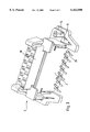
- FIG. 1 shows a printed circuit board according to the invention, with a coupling element of a plug-in device, in a perspective view,
- FIG. 2 shows the coupling element from FIG. 1 with a second, corresponding coupling element of the adjusting device, in an exploded representation
- FIG. 3 shows two coupling elements according to FIG. 2 inserted one in the other, without a printed circuit board, and
- FIG. 4 shows a partially sectional side view of the printed circuit board from FIG. 1.
- FIG. 1 shows a detail of a printed circuit board 1 of an instrument cluster of a motor vehicle.
- the printed circuit board 1 has in a clearance (aperture) 4 a coupling element 2 of a plug-in device.
- clearances mean apertures, passageways, openings, holes, slots, slits, cavities, recesses or the like.
- the coupling element 2 is in this case designed as a male multipoint connector.
- clearances (openings) 35 serve for receiving lighting elements (not shown), for example bulbs, for illuminating displays of the instrument cluster.
- the coupling element 2 is provided in its interior with a plurality of terminal contacts 5, the first end regions of which are arranged in a coupling region 7 of the coupling element 2, for electrical connection with a corresponding coupling element (not shown here), which can be inserted into the coupling region 7 of the coupling element 2.
- the coupling element 2 has a base 6, which serves for the mechanical connection of the coupling element 2 to the printed circuit board 1.
- the base 6 has on each of two opposite sides a flange 15, the flanges 15 extending approximately parallel to the printed circuit board 1, bearing against the latter and thus supporting the coupling element 2 on the printed circuit board 1.
- the free end 26 of the pins 14 has a shape tapering conically in the direction of insertion of the coupling element 2 into the printed circuit board 1, so that an automatic positioning of the coupling element 2 takes place.
- the flanges 15 of the base 6 bear against the side 8 of the printed circuit board 1 facing away from the coupling region 7 of the coupling element 2.
- the printed circuit board 1 is laminated, that is to say is provided with conductor tracks (not shown here).
- a lamination may also be provided on a side 9 of the printed circuit board 1 facing the coupling region 7.
- FIG. 1 also reveals two slit-shaped clearances (slits) 10, the alignment of which is described by center axes 36 and which respectively receive a connecting element 12 of the coupling element 2.
- the center axis 36 of one clearance 10 is in this case arranged at an angle ⁇ of about 20° with respect to the transverse extent of the approximately planar connecting element 12.
- the connecting element 12 is of a wedge-shaped design and has at its end away from the tip a fastening portion 18, by which it is inserted into an open slot 19 in the base 6 of the coupling element 2.
- the connecting element 12 may be held in the open slot 19 of its own accord, for example on account of a slight convexity of its own, but it may additionally be fixed by adhesive.
- the connecting element 12 is a sheet-metal component, and the coupling element 2 designed as a male multipoint connector is injection-molded from a plastic; during the joining of the coupling element 2 and connecting element 12, lugs 41 laterally on the fastening portion 18 therefore dig into the plastic of the coupling element 2 and securely hold the connecting element 12.
- each connecting element 12 runs with insertion edges 39 and 40 of an inserting and holding portion 16 on side edges of the slit-shaped clearance (slit) 10.
- said connecting element is twisted about a torsion axis 11 running in its longitudinal direction. This twisting in the direction of twisting T indicated in FIG.
- the coupling element 2 has in the longitudinal direction a multiplicity of through-clearances (terminal passageways) 20, into which L-shaped terminal contacts 5 are inserted and stabilized in grooves 27.
- a first leg 21 of the L-shaped terminal contacts 5 is contacted with a printed circuit board (not shown here) and a second leg 22 of the L ends in the coupling region 7 of the coupling element 2.
- the leg 21 contacted with the printed circuit board is provided in the contacting region with a bend 25, so that it bears against the printed circuit board with a point contact or a linear contact, perpendicular to the direction in which the leg 21 extends.
- a second coupling element 28 which is designed in the form of a female multipoint connector, corresponds to the first coupling element 2 and can be inserted into the latter.
- the second coupling element 28 has a plurality of longitudinally directed clearances (cavities) 29.
- the clearances 29 have in each case an additional clearance (slot) 32, perpendicularly to the direction in which they extend.
- Inserted into the clearances 29 are terminal contacts 30, which serve for the contacting with terminal contacts 5 of the first coupling element 2.
- the terminal contacts 30 are provided in each case in a side region with a spring tab 31, which engages in the lateral clearance (slot) 32 of the clearances (cavities) 29 and locks the terminal contacts 30 securely in the coupling element 28.
- the terminal contacts 30 are additionally locked by means of a bar 34, which is pushed into a groove 33 running part of the way around the outside of the coupling element 28.
- the first coupling element 2 has in its coupling region 7 a groove 23 running part of the way around it and into which a clip 24 is inserted.
- the clip 24 locks the first coupling element 2 and the second coupling element 28 when they have been joined together.
- a corresponding plug-in connection 3 with the first coupling element 2 and the second coupling element 28 inserted therein is shown in fig. 3, but for the sake of overall clarity without a printed circuit board.
Abstract
Description
Claims (23)
Applications Claiming Priority (2)
| Application Number | Priority Date | Filing Date | Title |
|---|---|---|---|
| DE19816126A DE19816126A1 (en) | 1998-04-09 | 1998-04-09 | Printed circuit board with a coupling element of a plug device |
| DE19816126 | 1998-04-09 |
Publications (1)
| Publication Number | Publication Date |
|---|---|
| US6162090A true US6162090A (en) | 2000-12-19 |
Family
ID=7864251
Family Applications (1)
| Application Number | Title | Priority Date | Filing Date |
|---|---|---|---|
| US09/288,383 Expired - Lifetime US6162090A (en) | 1998-04-09 | 1999-04-08 | Printed circuit board with a coupling element of a plug-in device |
Country Status (4)
| Country | Link |
|---|---|
| US (1) | US6162090A (en) |
| EP (1) | EP0949720B1 (en) |
| BR (1) | BRPI9901244B1 (en) |
| DE (2) | DE19816126A1 (en) |
Cited By (12)
| Publication number | Priority date | Publication date | Assignee | Title |
|---|---|---|---|---|
| EP1239546A2 (en) * | 2001-02-15 | 2002-09-11 | Tyco Electronics Raychem K.K. | Bottom entry connector |
| US6461168B2 (en) * | 1999-12-21 | 2002-10-08 | Mannesmann Vdo Ag | Plug socket for a display instrument |
| US20040203290A1 (en) * | 2003-04-14 | 2004-10-14 | Ya-Mei Wang | Connector structure |
| US20040253842A1 (en) * | 2003-06-11 | 2004-12-16 | Hewlett-Packard Development Company, L.P. | Backplane support system |
| US20060178037A1 (en) * | 2005-02-04 | 2006-08-10 | Fci Technology, Inc. | Strain relief for ball grid array connectors |
| EP1701412A1 (en) * | 2005-03-11 | 2006-09-13 | Huawei Technologies Co., Ltd. | Connector interface |
| GB2435339A (en) * | 2006-02-17 | 2007-08-22 | Xtag Ltd | Tamper proof security device with tag and strap |
| US20090258535A1 (en) * | 2008-04-10 | 2009-10-15 | Chamuel Steve R | Connector and receptacle therefor |
| US20100151727A1 (en) * | 2008-12-15 | 2010-06-17 | Hon Hai Precision Industry Co., Ltd. | Electrical connector incorporated with nut having barbs |
| US20130146270A1 (en) * | 2011-12-13 | 2013-06-13 | Delta Electronics (Shanghai) Co., Ltd. | Fixing device, and heat sink device or shield case comprising the same |
| US20190229450A1 (en) * | 2018-01-25 | 2019-07-25 | Lumberg Connect Gmbh | Plug connector with secondary safety |
| US11402058B2 (en) * | 2019-05-14 | 2022-08-02 | Field Energy Ops, Inc. | Boltless module support structures and boltless module attachment method |
Citations (3)
| Publication number | Priority date | Publication date | Assignee | Title |
|---|---|---|---|---|
| US4076165A (en) * | 1976-06-03 | 1978-02-28 | Motorola, Inc. | Mounting arrangement for chassis and printed circuit board with method of assembly |
| JPH0730277A (en) * | 1993-07-12 | 1995-01-31 | Toshiba Corp | Shielding device |
| US5540598A (en) * | 1994-06-16 | 1996-07-30 | The Whitaker Corporation | Pin spacer for an electrical connector |
Family Cites Families (5)
| Publication number | Priority date | Publication date | Assignee | Title |
|---|---|---|---|---|
| DE1625462A1 (en) * | 1967-10-05 | 1970-07-23 | Standard Elek K Lorenz Ag | Detachable connection |
| US4954085A (en) * | 1987-07-24 | 1990-09-04 | Honda Giken Kogyo Kabushiki Kaisha | Wiring structure |
| US4843714A (en) * | 1988-03-15 | 1989-07-04 | Amp Incorporated | Multiple line, automatic key programming and connector transfer system |
| DE8804956U1 (en) * | 1988-04-15 | 1988-06-09 | Harting Elektronik Gmbh, 4992 Espelkamp, De | |
| JPH05226042A (en) * | 1992-02-13 | 1993-09-03 | Nippon Denso Co Ltd | Connector |
-
1998
- 1998-04-09 DE DE19816126A patent/DE19816126A1/en active Pending
-
1999
- 1999-03-17 EP EP99105428A patent/EP0949720B1/en not_active Expired - Lifetime
- 1999-03-17 DE DE59913214T patent/DE59913214D1/en not_active Expired - Lifetime
- 1999-04-08 US US09/288,383 patent/US6162090A/en not_active Expired - Lifetime
- 1999-04-08 BR BRPI9901244-8A patent/BRPI9901244B1/en not_active IP Right Cessation
Patent Citations (3)
| Publication number | Priority date | Publication date | Assignee | Title |
|---|---|---|---|---|
| US4076165A (en) * | 1976-06-03 | 1978-02-28 | Motorola, Inc. | Mounting arrangement for chassis and printed circuit board with method of assembly |
| JPH0730277A (en) * | 1993-07-12 | 1995-01-31 | Toshiba Corp | Shielding device |
| US5540598A (en) * | 1994-06-16 | 1996-07-30 | The Whitaker Corporation | Pin spacer for an electrical connector |
Cited By (20)
| Publication number | Priority date | Publication date | Assignee | Title |
|---|---|---|---|---|
| US6461168B2 (en) * | 1999-12-21 | 2002-10-08 | Mannesmann Vdo Ag | Plug socket for a display instrument |
| EP1239546A3 (en) * | 2001-02-15 | 2004-01-21 | Tyco Electronics AMP K.K. | Bottom entry connector |
| EP1239546A2 (en) * | 2001-02-15 | 2002-09-11 | Tyco Electronics Raychem K.K. | Bottom entry connector |
| US20040203290A1 (en) * | 2003-04-14 | 2004-10-14 | Ya-Mei Wang | Connector structure |
| US20040253842A1 (en) * | 2003-06-11 | 2004-12-16 | Hewlett-Packard Development Company, L.P. | Backplane support system |
| US7095622B2 (en) | 2003-06-11 | 2006-08-22 | Hewlett-Packard Development Company, L.P. | Backplane support system with stiffener |
| US7341482B2 (en) * | 2005-02-04 | 2008-03-11 | Fci Americas Technology, Inc. | Strain relief for ball grid array connectors |
| US20060178037A1 (en) * | 2005-02-04 | 2006-08-10 | Fci Technology, Inc. | Strain relief for ball grid array connectors |
| US20080132111A1 (en) * | 2005-03-11 | 2008-06-05 | Huawei Technologies Co., Ltd. (People's Republic Of China) | Connector interface |
| EP1701412A1 (en) * | 2005-03-11 | 2006-09-13 | Huawei Technologies Co., Ltd. | Connector interface |
| US7713085B2 (en) | 2005-03-11 | 2010-05-11 | Huawei Technologies Co., Ltd. | Connector interface |
| GB2435339A (en) * | 2006-02-17 | 2007-08-22 | Xtag Ltd | Tamper proof security device with tag and strap |
| GB2435339B (en) * | 2006-02-17 | 2008-12-17 | Xtag Ltd | Security device |
| US20090258535A1 (en) * | 2008-04-10 | 2009-10-15 | Chamuel Steve R | Connector and receptacle therefor |
| US7686660B2 (en) * | 2008-04-10 | 2010-03-30 | Osram Sylvania Inc. | Connector and receptacle therefor |
| US20100151727A1 (en) * | 2008-12-15 | 2010-06-17 | Hon Hai Precision Industry Co., Ltd. | Electrical connector incorporated with nut having barbs |
| US20130146270A1 (en) * | 2011-12-13 | 2013-06-13 | Delta Electronics (Shanghai) Co., Ltd. | Fixing device, and heat sink device or shield case comprising the same |
| US20190229450A1 (en) * | 2018-01-25 | 2019-07-25 | Lumberg Connect Gmbh | Plug connector with secondary safety |
| US10665972B2 (en) * | 2018-01-25 | 2020-05-26 | Lumberg Connect Gmbh | Plug connector with secondary safety |
| US11402058B2 (en) * | 2019-05-14 | 2022-08-02 | Field Energy Ops, Inc. | Boltless module support structures and boltless module attachment method |
Also Published As
| Publication number | Publication date |
|---|---|
| EP0949720B1 (en) | 2006-03-15 |
| BR9901244A (en) | 2000-03-14 |
| BRPI9901244B1 (en) | 2015-08-18 |
| EP0949720A3 (en) | 2000-12-06 |
| DE19816126A1 (en) | 1999-11-04 |
| DE59913214D1 (en) | 2006-05-11 |
| EP0949720A2 (en) | 1999-10-13 |
Similar Documents
| Publication | Publication Date | Title |
|---|---|---|
| US9263820B2 (en) | Electrical press-fit pin for a semiconductor module | |
| US5154634A (en) | Connector holding device | |
| US7722366B2 (en) | Board-mounted electrical connector | |
| US6162090A (en) | Printed circuit board with a coupling element of a plug-in device | |
| JP3013756B2 (en) | Board connector | |
| US6839240B2 (en) | Housing for an electronic control device in motor vehicles | |
| JP7361839B2 (en) | connector | |
| JPH06215835A (en) | Surface mount type electrical connector | |
| US10893615B2 (en) | Printed circuit board composite and method for producing same | |
| US20090104802A1 (en) | Electrical connector assembly | |
| EP0245161A1 (en) | Fixing structure for contact pins of electrical connector | |
| JPH0757822A (en) | Connector | |
| US20090156044A1 (en) | Electrical Connector and Contact Insertion Guide | |
| US9954327B1 (en) | Modular PCB housing with grounding clip | |
| US4875862A (en) | Surface mountable connector | |
| US20230006392A1 (en) | Connection strip and method of manufacturing the connection strip | |
| US20230061365A1 (en) | Printed circuit board corner connection | |
| CN111213285B (en) | Solder contact, contact module and method for producing a contact module | |
| JPH1012342A (en) | Contact and ic socket provided with the contact | |
| CN109075474B (en) | Electrical connector and electrical connection method | |
| JPH0511663Y2 (en) | ||
| JPH026635Y2 (en) | ||
| JPH0722487U (en) | Connector socket | |
| JP2005318693A (en) | Connection structure and method of press-fit terminal and bus bar | |
| JP3781319B2 (en) | Flat cable fixing clip |
Legal Events
| Date | Code | Title | Description |
|---|---|---|---|
| AS | Assignment |
Owner name: MANNESMANN VDO AG, GERMANY Free format text: ASSIGNMENT OF ASSIGNORS INTEREST;ASSIGNORS:KLUBENSPIES, DIETER;ZEISS, MANFRED;REEL/FRAME:010074/0878 Effective date: 19990519 |
|
| STCF | Information on status: patent grant |
Free format text: PATENTED CASE |
|
| FPAY | Fee payment |
Year of fee payment: 4 |
|
| FEPP | Fee payment procedure |
Free format text: PAYOR NUMBER ASSIGNED (ORIGINAL EVENT CODE: ASPN); ENTITY STATUS OF PATENT OWNER: LARGE ENTITY |
|
| FPAY | Fee payment |
Year of fee payment: 8 |
|
| AS | Assignment |
Owner name: SIEMENS AKTIENGESELLSCHAFT, GERMANY Free format text: MERGER;ASSIGNOR:MANNESMANN VDO AKTIENGESELLSCHAFT;REEL/FRAME:026005/0303 Effective date: 20100315 |
|
| AS | Assignment |
Owner name: CONTINENTAL AUTOMOTIVE GMBH, GERMANY Free format text: ASSIGNMENT OF ASSIGNORS INTEREST;ASSIGNOR:SIEMENS AKTIENGESELLSCHAFT;REEL/FRAME:027263/0068 Effective date: 20110704 |
|
| FPAY | Fee payment |
Year of fee payment: 12 |