US6165908A - Single-layer-electrode type charge coupled device having double conductive layers for charge transfer electrodes - Google Patents
Single-layer-electrode type charge coupled device having double conductive layers for charge transfer electrodes Download PDFInfo
- Publication number
- US6165908A US6165908A US09/535,734 US53573400A US6165908A US 6165908 A US6165908 A US 6165908A US 53573400 A US53573400 A US 53573400A US 6165908 A US6165908 A US 6165908A
- Authority
- US
- United States
- Prior art keywords
- layer
- insulating layer
- silicon oxide
- conductive layer
- charge transfer
- Prior art date
- Legal status (The legal status is an assumption and is not a legal conclusion. Google has not performed a legal analysis and makes no representation as to the accuracy of the status listed.)
- Expired - Fee Related
Links
- 239000004065 semiconductor Substances 0.000 claims abstract description 31
- 239000000758 substrate Substances 0.000 claims abstract description 16
- VYPSYNLAJGMNEJ-UHFFFAOYSA-N Silicium dioxide Chemical compound O=[Si]=O VYPSYNLAJGMNEJ-UHFFFAOYSA-N 0.000 claims description 52
- 229910052814 silicon oxide Inorganic materials 0.000 claims description 52
- 238000000034 method Methods 0.000 claims description 32
- 229910052751 metal Inorganic materials 0.000 claims description 17
- 239000002184 metal Substances 0.000 claims description 17
- 238000005530 etching Methods 0.000 claims description 9
- 238000004519 manufacturing process Methods 0.000 claims description 9
- 229910021420 polycrystalline silicon Inorganic materials 0.000 claims description 9
- 229920002120 photoresistant polymer Polymers 0.000 claims description 4
- 239000003870 refractory metal Substances 0.000 claims description 4
- 229910052581 Si3N4 Inorganic materials 0.000 claims description 3
- 229910021332 silicide Inorganic materials 0.000 claims description 3
- FVBUAEGBCNSCDD-UHFFFAOYSA-N silicide(4-) Chemical compound [Si-4] FVBUAEGBCNSCDD-UHFFFAOYSA-N 0.000 claims description 3
- HQVNEWCFYHHQES-UHFFFAOYSA-N silicon nitride Chemical compound N12[Si]34N5[Si]62N3[Si]51N64 HQVNEWCFYHHQES-UHFFFAOYSA-N 0.000 claims description 3
- 238000000059 patterning Methods 0.000 claims 1
- 239000010410 layer Substances 0.000 description 162
- WQJQOUPTWCFRMM-UHFFFAOYSA-N tungsten disilicide Chemical compound [Si]#[W]#[Si] WQJQOUPTWCFRMM-UHFFFAOYSA-N 0.000 description 11
- 229910021342 tungsten silicide Inorganic materials 0.000 description 11
- 238000005229 chemical vapour deposition Methods 0.000 description 8
- 230000003247 decreasing effect Effects 0.000 description 8
- 230000001419 dependent effect Effects 0.000 description 6
- 238000009413 insulation Methods 0.000 description 5
- 238000000206 photolithography Methods 0.000 description 4
- 238000009825 accumulation Methods 0.000 description 3
- 230000015556 catabolic process Effects 0.000 description 3
- 230000003071 parasitic effect Effects 0.000 description 3
- 238000005036 potential barrier Methods 0.000 description 3
- 238000001444 catalytic combustion detection Methods 0.000 description 2
- 238000010586 diagram Methods 0.000 description 2
- 230000000694 effects Effects 0.000 description 2
- 229910021421 monocrystalline silicon Inorganic materials 0.000 description 2
- 239000002356 single layer Substances 0.000 description 2
- 230000005641 tunneling Effects 0.000 description 2
- ZOKXTWBITQBERF-UHFFFAOYSA-N Molybdenum Chemical compound [Mo] ZOKXTWBITQBERF-UHFFFAOYSA-N 0.000 description 1
- XUIMIQQOPSSXEZ-UHFFFAOYSA-N Silicon Chemical compound [Si] XUIMIQQOPSSXEZ-UHFFFAOYSA-N 0.000 description 1
- RTAQQCXQSZGOHL-UHFFFAOYSA-N Titanium Chemical compound [Ti] RTAQQCXQSZGOHL-UHFFFAOYSA-N 0.000 description 1
- YXTPWUNVHCYOSP-UHFFFAOYSA-N bis($l^{2}-silanylidene)molybdenum Chemical compound [Si]=[Mo]=[Si] YXTPWUNVHCYOSP-UHFFFAOYSA-N 0.000 description 1
- 230000004048 modification Effects 0.000 description 1
- 238000012986 modification Methods 0.000 description 1
- 229910052750 molybdenum Inorganic materials 0.000 description 1
- 239000011733 molybdenum Substances 0.000 description 1
- 229910021344 molybdenum silicide Inorganic materials 0.000 description 1
- 229910052710 silicon Inorganic materials 0.000 description 1
- 239000010703 silicon Substances 0.000 description 1
- 239000010936 titanium Substances 0.000 description 1
- 229910052719 titanium Inorganic materials 0.000 description 1
- 229910021341 titanium silicide Inorganic materials 0.000 description 1
- WFKWXMTUELFFGS-UHFFFAOYSA-N tungsten Chemical compound [W] WFKWXMTUELFFGS-UHFFFAOYSA-N 0.000 description 1
- 229910052721 tungsten Inorganic materials 0.000 description 1
- 239000010937 tungsten Substances 0.000 description 1
Images


Classifications
-
- H—ELECTRICITY
- H01—ELECTRIC ELEMENTS
- H01L—SEMICONDUCTOR DEVICES NOT COVERED BY CLASS H10
- H01L27/00—Devices consisting of a plurality of semiconductor or other solid-state components formed in or on a common substrate
- H01L27/14—Devices consisting of a plurality of semiconductor or other solid-state components formed in or on a common substrate including semiconductor components sensitive to infrared radiation, light, electromagnetic radiation of shorter wavelength or corpuscular radiation and specially adapted either for the conversion of the energy of such radiation into electrical energy or for the control of electrical energy by such radiation
- H01L27/144—Devices controlled by radiation
- H01L27/146—Imager structures
- H01L27/148—Charge coupled imagers
- H01L27/14806—Structural or functional details thereof
- H01L27/14812—Special geometry or disposition of pixel-elements, address lines or gate-electrodes
-
- H—ELECTRICITY
- H01—ELECTRIC ELEMENTS
- H01L—SEMICONDUCTOR DEVICES NOT COVERED BY CLASS H10
- H01L29/00—Semiconductor devices adapted for rectifying, amplifying, oscillating or switching, or capacitors or resistors with at least one potential-jump barrier or surface barrier, e.g. PN junction depletion layer or carrier concentration layer; Details of semiconductor bodies or of electrodes thereof ; Multistep manufacturing processes therefor
- H01L29/66—Types of semiconductor device ; Multistep manufacturing processes therefor
- H01L29/68—Types of semiconductor device ; Multistep manufacturing processes therefor controllable by only the electric current supplied, or only the electric potential applied, to an electrode which does not carry the current to be rectified, amplified or switched
- H01L29/76—Unipolar devices, e.g. field effect transistors
- H01L29/762—Charge transfer devices
- H01L29/765—Charge-coupled devices
- H01L29/768—Charge-coupled devices with field effect produced by an insulated gate
Definitions
- the present invention relates to a single-layer-electrode type charge coupled device (CCD) and a method for manufacturing the same.
- the electrodes can be made of metal or silicide in addition to polycrystalline silicon, to further reduce the resistances of the electrodes.
- a plurality of charge transfer electrodes are formed on a first insulating layer formed on a semiconductor substrate. Double conductive layers are formed on the first insulating layer. A second insulating layer is formed on the double conductive layers, and the second insulating layer is patterned by a photolithography and etching process. In addition, a sidewall insulating layer is formed on a sidewall of the patterned second insulating layer. The double conductive layers are etched by using the sidewall insulating layer as well as the second insulating layer as a mask, thus forming charge transfer electrodes (see: N.
- the spacing between the charge transfer electrodes is decreased by providing the sidewall insulating layer on the sidewall of the second insulating layer.
- the width of the sidewall insulating layer is generally dependent upon only the thickness of the second insulating layer.
- the thickness of the second insulating layer is increased, the step coverage characteristics of the overlying insulating layer are deteriorated, so that metal wiring layers are disconnected and the insulation breakdown characteristics between the charge transfer electrodes and the metal wiring layers are deteriorated.
- Another object is to provide a method for manufacturing the above-mentioned CCD.
- a plurality of charge transfer electrodes are formed on a first insulating layer formed on a semiconductor substrate.
- Each of the charge transfer electrodes is formed by a first conductive layer and a second conductive layer narrower than the first conductive layer.
- a second insulating layer having the same area of the second conductive layer and is formed on the second conductive layer.
- a sidewall insulating layer is formed on sidewalls of the second insulating layer and the second conductive layer.
- the width of the sidewall insulating layer is dependent upon the thickness of the second insulating layer and the thickness of the second conductive layer.
- a plurality of charge transfer electrodes are formed on a first insulating layer formed on a semiconductor substrate. Double conductive layers are formed on the first insulating layer. A second insulating layer is formed on the double conductive layers, and the second insulating layer and the upper layer of the double conductive layers are patterned by the same mask. In addition, a sidewall insulating layer is formed on a sidewall of the patterned second insulating layer and the upper layer of the double conductive layers. The lower layer of the double conductive layers is etched by using the sidewall insulating layer as well as the second insulating layer as a mask, thus forming charge transfer electrodes.
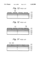
- FIGS. 1A and 1J are cross-sectional views for explaining a prior art method for manufacturing a single-layer-electrode type two-phase CCD;
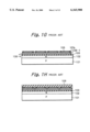
- FIG. 2A is a cross-sectional view showing the operation of the CCD of FIG. 1J;
- FIG. 2B is a potential diagram of the CCD of FIG. 2A;
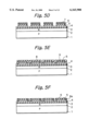
- FIGS. 3 and 4 are cross-sectional views for explaining the problems in the prior art method of FIGS. 1A and 1J;
- FIGS. 5A through 5J are cross-sectional views for explaining an embodiment of the method for manufacturing a single-layer-electrode type two-phase CCD according to the present invention.
- FIG. 6A is a cross-sectional view showing the operation of the CCD of FIG. 5J;
- FIG. 6B is a potential diagram of the CCD of FIG. 6A.
- FIG. 7 is a cross-sectional view illustrating a modification of the CCD of FIG. 6A.
- FIGS. 1A through 1J Before the description of the preferred embodiment, a method for manufacturing a single-layer-electrode type two-phase CCD will be explained with reference to FIGS. 1A through 1J (see: N. Tanaka et al., "Study of Single-Layer Metal-Electrode CCD Image Sensor", Proceedings of the Institude of Television Engineers of Japan, Vol. 50, No. 2, pp. 234-240, 1996). Note that the CCD of FIGS. 1A through 1J is of a burled channel type.
- an N-type semiconductor layer 102 is formed on a P-type semiconductor substrate 101 formed by monocrystalline silicon. Then, the semiconductor substrate 101 (the N-type semiconductor layer 102) is thermally oxidized to form a silicon oxide layer. Also, a silicon layer and a silicon oxide layer are deposited thereon to an insulating layer 103 of a triple-strudure.
- an about 0.1 ⁇ m thick polycrystalline silicon layer 104 and an about 0.1 ⁇ m thick tungsten silicide layer 105 are deposited on the entire surface.
- an about 0.2 ⁇ m thick silicon oxide layer 106 is deposited on the entire surface by a chemical vapor deposition (CVD) process.
- CVD chemical vapor deposition
- the silicon oxide layer 106 is patterned by a photolithography and etching process.
- an about 0.2 ⁇ m thick silicon oxide layer 107 is deposited on the entire surface by a CVD process.
- the silicon oxide layer 107 is etched back by an anisotropic etching process. As a result, the silicon oxide layer 107 is left as a sidewall silicon oxide layer 107a on a sidewall of the silicon oxide layer 106.
- the tungsten silicide layer 105 and the polycrystalline silicon layer 104 are patterned by an etching process using the silicon oxide layer 106 and the sidewall silicon oxide layer 107a as a mask to form charge transfer electrodes 108-1, . . . , 108-4 whose spacing is about 0.2 ⁇ m.
- an insulating layer 109 is deposited on the entire surface by a CVD process.
- metal wiring layers 110-1, 110-2, 110-3 and 110-4 are formed and connected to the charge transfer electrodes 108-1, 108-2, 108-3 and 108-4, respectively.
- a reverse bias voltage V D is applied between the semiconductor substrate 101 and the N-type semiconductor layer 102, so that the N-type semiconductor layer 102 becomes in an electron accumulation state.
- a positive pulse voltage+V w such as +40V is applied to the metal wiring layers 101-1 and 101-3.
- V w positive pulse voltage
- electrons are injected from the N-type semiconductor layer 102 into the insulating layer layer 103 under the charge transfer electrodes 108-1 and 108-3 by the tunneling effect. Therefore, electrons are trapped in the triple-structured insulating layer 103 urder the charge transfer electrodes 108-1 and 108-3.
- the electron-injected portions of the insulating layer 103 serving as potential barrier regions are in self-alignment with the charge transfer electrodes 108-1 and 108-3. Therefore, when clock signals .o slashed. 1 and .o slashed. 2 opposite in phase to each other are applied to the metal wiring layers 110-1 (110-2) and 110-3 (110-4), respectively, as shown in FIG. 2A, the potential within the device is as shown in FIG. 2B.
- the spacing between the charge transfer electrodes 108-1, 108-2, . . . is decreased by providing the sidewall silicon oxide layer 107a on the sidewall of the silicon oxide layer 106.
- the width of the sidewall silicon oxide layer 107a is generally dependent upon only the thickness of the silicon oxide layer 106. That is, the larger the thickness of the silicon oxide layer 106, the larger the width of the sidewall silicon oxide layer 107a.
- the step coverage characteristics of the insulating layer 109 are deteriorated, so that the metal wiring layers 110-1, 110-2, 110-3 and 110-4 are disconnected and the insulation breakdown characteristics between the charge transfer electrodes 108-1, 108-2, 108-3 and 108-4 and the metal wiring layers 110-1, 110-2, 110-3 and 110-4 are deteriorated.
- FIGS. 5A through 5J An embodiment of the method for manufacturing a CCD according to the present invention will be explained with reference to FIGS. 5A through 5J. Not that the CCD of FIGS. 5A through 5J is of a buried channel type.
- an N-type semiconductor layer 2 is formed on a P-type semiconductor substrate 1 formed by monocrystalline silicon. Then, the semiconductor substrate 1 (the N-type semiconductor layer 2) is thermally oxidized to form an about 200 ⁇ thick silicon oxide layer. Also, an about 200 ⁇ thick silicon nitride layer and an about 500 ⁇ thick silicon oxide layer are deposited by a CVD process. In this case, a triple-structured insulating layer 3 mad of silicon oxide/silicon nitride/silicon oxide (ONO) is formed.
- an about 0.1 ⁇ m thick polycrystalline silicon layer 4 and an about 0.1 ⁇ m thick tungsten silicide layer 5 are deposited on the entire surface.
- an about 0.2 ⁇ m thick silicon oxide layer 6 is deposited on the entire surface by a CVD process.
- a photoresist pattern 7 is formed by a photolithography process. Then, the silicon oxide layer 6 and the tungsten silicide layer 5 are simultaneously etched by using the photoresist pattern 7 as a mask. Then, the photoresist pattern 7 is removed.
- an about 0.2 ⁇ m thick silicon oxide layer 7 is deposited on the entire surface by a CVD process.
- the silicon oxide layer 8 is etched back by an anisotropic etching process. As a result, the silicon oxide layer 8 is left as a sidewall silicon oxide layer 8a on a sidewall of the silicon oxide layer 106 and a sidewall of the tungsten silicide layer 5.
- the polycrystalline silicon layer 4 is etched by an etching process using the silicon oxide layer 6 and the sidewall silicon oxide layer 8a as a mask to form charge transfer electrodes 9-1, . . . , 9-4 whose spacing is about 0.2 ⁇ m.
- an insulating layer 10 is deposited on the entire surface by a CVD process.
- metal wiring layers 11-1, 11-2, 11-3 and 11-5 are formed and connected to the charge transfer electrodes 9-1, 9-2, 9-3 and 9-4, respectively.
- a reverse bias voltage V D is applied between the semiconductor substrate 1 and the N-type semiconductor layer 2, so that the N-type semiconductor layer 2 becomes in an electron accumulation state.
- a positive pulse voltage+V w such as +40V is applied to the metal wiring layers 11-1 and 11-3.
- V w positive pulse voltage
- electrons are injected from the N-type semiconductor layer 2 into the insulating layer 3 under the charge transfer electrodes 9-1 and 9-3 by the tunneling effect. Therefore, electrons are trapped in the insulating layer 3 under the charge transfer electrodes 9-1 and 9-3, particularly at the interface between the triple structure insulating layer under the charge transfer electrode 9-1 and 9-3.
- the electron-injected portions of the insulating layer 3 serving as potential barrier regions are in self-alignment with the charge transfer electrodes 9-1 and 9-3. Therefore, when clock signals .o slashed. 1 and .o slashed. 2 opposite in phase to each other are applied to the metal wiring layers 11-1 (11-2) and 11-3 (11-4), respectively, as shown in FIG. 6A, the potential within the device is as shown in FIG. 6B.
- the spacing between the charge transfer electrodes 9-1, 9-2, . . . is decreased by providing the sidewall silicon oxide layer 8a on the sidewall of the tungsten silicide layer 5 and the silicon oxide layer 6. Therefore, the width of the sidewall silicon oxide layer 8a is dependent upon a sum of the thickness of the tungsten silicide layer 5 and the thickness of the silicon oxide layer 6.
- the width of the sidewall silicon oxide layer 8a is remarkably larger than that of the sidewall silicon oxide layer 107a of the prior art CCD, so that the spacing between the charge transfer electrodes 9-1, 9-2, 9-3 and 9-4 can be decreased.
- the step coverage characteristics of the insulating layer 10 are not deteriorated, so that the disconnection of the metal wiring layers 11-1, 11-2, 11-3 and 11-4 can be avoided and the insulation breakdown characteristics between the charge transfer electrodes 9-1, 9-2, 9-3 and 9-4 and the metal wiring layers 11-1, 11-2, 11-3 and 11-4 are not deteriorated.
- the parasitic capacitance between the charge transfer electrodes 9-1, 9-2, 9-3 and 9-4 is substantially dependent only upon the area of the sidewall of the polycrystalline silicon layer 4, such parasitic capacitance can be decreased.
- the parasitic capacitance between the charge transfer electrodes 108-1, 108-2, 108-3 and 108-4 is substantially dependent only upon the area of the sidewall of the polycrystalline silicon layer 104 and the sidewall of the tungsten silicide layer 105.
- the tungsten silicide layer 5 is etched by using the polycrystalline silicon layer 4 as an etching stopper as illustrated in FIG. 5D, the accuracy of the etched tungsten silicide layer 5 becomes high, so that the fluctuation of the spacing between the charge transfer electrodes 9-1, 9-2, 9-3 and 9-4 can be suppressed.
- FIG. 5J although a positive pulse voltage+V w is applied to the metal wiring layers 11-1 and 11-3, it is possible to apply a negative pulse voltage-V w such as -40v to the metal wiring layers 11-1 and 11-3.
- a negative pulse voltage-V w such as -40v
- electrons are injected from charge transfer electrodes 9-1 and 9-3 into the silicon oxide layer 3 under the charge transfer electrodes 9-1 and 9-3. Therefore, electrons are trapped in the silicon oxide layer 3 under the charge transfer electrodes 9-1 and 9-3, particularly, at the interface of the triple-structured insulating layer.
- a refractory metal silicide layer made of molybdenum silicide or titanium silicide or a refractory metal layer made of tungsten, molybdenum or titanium can be used instead of the tungsten silicide layer 5.
- the present invention can be applied to a buried channel type P-channel CCD where the semiconductor substrate 1 is of an N-type and the semiconductor layer 2 is of a P-type.
- the present invention can be applied to a surface channel type CCD where the conductivity type of the semiconductor substrate 1 is the same as that of the semiconductor layer 2, or the semiconductor layer 2 is omitted so that the insulating layer 3 is formed directly on the semiconductor substrate 1 as illustrated in FIG. 7.
- the present invention can be applied to a single-layer-electrode type four-phase CCD.
- the triple-structured insulating layer 3 is replaced by a single insulating layer made of silicon oxide.
- holes can be injected.
- the hole injected portions below the charge transfer electrodes serve as charge accumulation regions, not as potential barrier regions.
- the CCD can be formed in a semiconductor well within a semiconductor substrate.
- the width of the sidewall insulating layer for decreasing the spacing between the charge transfer electrodes is increased, the spacing between the charge transfer electrodes can be remarkably decreased.
Abstract
In a charge coupled device, a plurality of charge transfer electrodes are formed on a first insulating layer formed on a semiconductor substrate. Each of the charge transfer electrodes is formed by a first conductive layer and a second conductive layer narrower than the first conductive layer. A second insulating layer having the same area as the second conductive layer and is formed on the second conductive layer. A sidewall insulating layer is formed on sidewalls of the second insulating layer and the second conductive layer.
Description
This application is a division of application Ser. No. 09/033,855, filed Mar. 3, 1998, now abandoned.
1. Field of the Invention
The present invention relates to a single-layer-electrode type charge coupled device (CCD) and a method for manufacturing the same.
2. Description of the Related Art
Recently, single-layer-electrode type CCDs have been developed by etching a single conductive layer with a fine photolithography and etching process to obtain electrodes whose spacing is about 0.2 to 0.3 μm.
In the single-layer-electrode CCDs, since no overlapping of the electrodes is present, a capacitance between the electrodes can be small and no poor insulation is present between the electrodes. Further, since it is unnecessary to oxidize the electrodes to obtain insulation thereof, the electrodes can be made of metal or silicide in addition to polycrystalline silicon, to further reduce the resistances of the electrodes.
In a prior art method for manufacturing a CCD, a plurality of charge transfer electrodes are formed on a first insulating layer formed on a semiconductor substrate. Double conductive layers are formed on the first insulating layer. A second insulating layer is formed on the double conductive layers, and the second insulating layer is patterned by a photolithography and etching process. In addition, a sidewall insulating layer is formed on a sidewall of the patterned second insulating layer. The double conductive layers are etched by using the sidewall insulating layer as well as the second insulating layer as a mask, thus forming charge transfer electrodes (see: N. Tanaka et al., "Study of Single-Layer Metal-Electrode CCD Image Sensor", Proceedings of the Institude of Television Engineers of Japan, Vol. 50, No. 2, pp. 234-240, 1996). This will be explained later in detail.
In the prior art method, the spacing between the charge transfer electrodes, is decreased by providing the sidewall insulating layer on the sidewall of the second insulating layer.
In the prior art method, however, in order to reduce the spacing between the charge transfer electrodes it is impossible to increase the width of the sidewall insulating layer. In other words, the width of the sidewall insulating layer is generally dependent upon only the thickness of the second insulating layer.
On the other hand, when the thickness of the second insulating layer is increased, the step coverage characteristics of the overlying insulating layer are deteriorated, so that metal wiring layers are disconnected and the insulation breakdown characteristics between the charge transfer electrodes and the metal wiring layers are deteriorated.
It is an object of the present invention to provide a single-layer-electrode type CCD capable of decreasing the spacing between charge transfer electrodes.
Another object is to provide a method for manufacturing the above-mentioned CCD.
According to the present invention, in a charge coupled device, a plurality of charge transfer electrodes are formed on a first insulating layer formed on a semiconductor substrate. Each of the charge transfer electrodes is formed by a first conductive layer and a second conductive layer narrower than the first conductive layer. A second insulating layer having the same area of the second conductive layer and is formed on the second conductive layer. A sidewall insulating layer is formed on sidewalls of the second insulating layer and the second conductive layer. Thus, the width of the sidewall insulating layer is dependent upon the thickness of the second insulating layer and the thickness of the second conductive layer.
Also, in a method for manufacturing CCD, a plurality of charge transfer electrodes are formed on a first insulating layer formed on a semiconductor substrate. Double conductive layers are formed on the first insulating layer. A second insulating layer is formed on the double conductive layers, and the second insulating layer and the upper layer of the double conductive layers are patterned by the same mask. In addition, a sidewall insulating layer is formed on a sidewall of the patterned second insulating layer and the upper layer of the double conductive layers. The lower layer of the double conductive layers is etched by using the sidewall insulating layer as well as the second insulating layer as a mask, thus forming charge transfer electrodes.
The present invention will be more clearly understood from the description as set forth below, with reference to the accompanying drawings, wherein:
FIGS. 1A and 1J are cross-sectional views for explaining a prior art method for manufacturing a single-layer-electrode type two-phase CCD;
FIG. 2A is a cross-sectional view showing the operation of the CCD of FIG. 1J;
FIG. 2B is a potential diagram of the CCD of FIG. 2A;
FIGS. 3 and 4 are cross-sectional views for explaining the problems in the prior art method of FIGS. 1A and 1J;
FIGS. 5A through 5J are cross-sectional views for explaining an embodiment of the method for manufacturing a single-layer-electrode type two-phase CCD according to the present invention;
FIG. 6A is a cross-sectional view showing the operation of the CCD of FIG. 5J;
FIG. 6B is a potential diagram of the CCD of FIG. 6A; and
FIG. 7 is a cross-sectional view illustrating a modification of the CCD of FIG. 6A.
Before the description of the preferred embodiment, a method for manufacturing a single-layer-electrode type two-phase CCD will be explained with reference to FIGS. 1A through 1J (see: N. Tanaka et al., "Study of Single-Layer Metal-Electrode CCD Image Sensor", Proceedings of the Institude of Television Engineers of Japan, Vol. 50, No. 2, pp. 234-240, 1996). Note that the CCD of FIGS. 1A through 1J is of a burled channel type.
First, referring to FIG. 1A, an N-type semiconductor layer 102 is formed on a P-type semiconductor substrate 101 formed by monocrystalline silicon. Then, the semiconductor substrate 101 (the N-type semiconductor layer 102) is thermally oxidized to form a silicon oxide layer. Also, a silicon layer and a silicon oxide layer are deposited thereon to an insulating layer 103 of a triple-strudure.
Next, referring to FIG. 1B, an about 0.1 μm thick polycrystalline silicon layer 104 and an about 0.1 μm thick tungsten silicide layer 105 are deposited on the entire surface.
Next, referring to FIG. 1C, an about 0.2 μm thick silicon oxide layer 106 is deposited on the entire surface by a chemical vapor deposition (CVD) process.
Next, referring to FIG. 1D, the silicon oxide layer 106 is patterned by a photolithography and etching process.
Next, referring to FIG. 1E, an about 0.2 μm thick silicon oxide layer 107 is deposited on the entire surface by a CVD process.
Next, referring to FIG. 1F, the silicon oxide layer 107 is etched back by an anisotropic etching process. As a result, the silicon oxide layer 107 is left as a sidewall silicon oxide layer 107a on a sidewall of the silicon oxide layer 106.
Next, referring to FIG. 1G, the tungsten silicide layer 105 and the polycrystalline silicon layer 104 are patterned by an etching process using the silicon oxide layer 106 and the sidewall silicon oxide layer 107a as a mask to form charge transfer electrodes 108-1, . . . , 108-4 whose spacing is about 0.2 μm.
Next, referring to FIG. 1H, an insulating layer 109 is deposited on the entire surface by a CVD process.
Next, referring to FIG. 1I, metal wiring layers 110-1, 110-2, 110-3 and 110-4 are formed and connected to the charge transfer electrodes 108-1, 108-2, 108-3 and 108-4, respectively.
Finally, referring to FIG. 1J, a reverse bias voltage VD is applied between the semiconductor substrate 101 and the N-type semiconductor layer 102, so that the N-type semiconductor layer 102 becomes in an electron accumulation state. In this state, a positive pulse voltage+Vw such as +40V is applied to the metal wiring layers 101-1 and 101-3. As a result, electrons are injected from the N-type semiconductor layer 102 into the insulating layer layer 103 under the charge transfer electrodes 108-1 and 108-3 by the tunneling effect. Therefore, electrons are trapped in the triple-structured insulating layer 103 urder the charge transfer electrodes 108-1 and 108-3.
Thus, in the prior art CCD, the electron-injected portions of the insulating layer 103 serving as potential barrier regions are in self-alignment with the charge transfer electrodes 108-1 and 108-3. Therefore, when clock signals .o slashed.1 and .o slashed.2 opposite in phase to each other are applied to the metal wiring layers 110-1 (110-2) and 110-3 (110-4), respectively, as shown in FIG. 2A, the potential within the device is as shown in FIG. 2B.
In the prior art CCD of FIGS. 1A through 1J, 2A and 2B, the spacing between the charge transfer electrodes 108-1, 108-2, . . . is decreased by providing the sidewall silicon oxide layer 107a on the sidewall of the silicon oxide layer 106.
In the prior art CCD of FIGS. 1A through 1J, 2A and 2B, however, in order to reduce the spacing between the charge transfer electrodes 108-1, 108-2, . . . , even when the thickness T of the silicon oxide layer 107 is increased, it is impossible to increase the width W of the sidewall silicon oxide layer 107a. For example, as shown in FIG. 3, if the thickness of the silicon oxide layer 107 is T1, the width of the sidewall silicon oxide layer 107a is W1. On the other hand, as shown in FIG. 4, if the thickness of the silicon oxide layer 107 is T2 (>T1), the width of the sidewall silicon oxide layer 107a W2. In this case, if T1 >T0 (critical value),
W.sub.1 ⃡W.sub.2.
Note that the width of the sidewall silicon oxide layer 107a is generally dependent upon only the thickness of the silicon oxide layer 106. That is, the larger the thickness of the silicon oxide layer 106, the larger the width of the sidewall silicon oxide layer 107a.
On the other hand, when the thickness of the silicon oxide layer 106 is increased, the step coverage characteristics of the insulating layer 109 are deteriorated, so that the metal wiring layers 110-1, 110-2, 110-3 and 110-4 are disconnected and the insulation breakdown characteristics between the charge transfer electrodes 108-1, 108-2, 108-3 and 108-4 and the metal wiring layers 110-1, 110-2, 110-3 and 110-4 are deteriorated.
An embodiment of the method for manufacturing a CCD according to the present invention will be explained with reference to FIGS. 5A through 5J. Not that the CCD of FIGS. 5A through 5J is of a buried channel type.
First, referring to FIG. 5A, in the same way as in FIG. 1A, an N-type semiconductor layer 2 is formed on a P-type semiconductor substrate 1 formed by monocrystalline silicon. Then, the semiconductor substrate 1 (the N-type semiconductor layer 2) is thermally oxidized to form an about 200 Å thick silicon oxide layer. Also, an about 200 Å thick silicon nitride layer and an about 500 Å thick silicon oxide layer are deposited by a CVD process. In this case, a triple-structured insulating layer 3 mad of silicon oxide/silicon nitride/silicon oxide (ONO) is formed.
Next, referring to FIG. 5B, in the same way as in FIG. 1B, an about 0.1 μm thick polycrystalline silicon layer 4 and an about 0.1 μm thick tungsten silicide layer 5 are deposited on the entire surface.
Next, referring to FIG. 5C, in the same way as in FIG. 1C, an about 0.2 μm thick silicon oxide layer 6 is deposited on the entire surface by a CVD process.
Next, referring to FIG. 5D, a photoresist pattern 7 is formed by a photolithography process. Then, the silicon oxide layer 6 and the tungsten silicide layer 5 are simultaneously etched by using the photoresist pattern 7 as a mask. Then, the photoresist pattern 7 is removed.
Next, referring to FIG. 5E, in the same way as in FIG. 1E, an about 0.2 μm thick silicon oxide layer 7 is deposited on the entire surface by a CVD process.
Next, referring to FIG. 5F, in the same way as in FIG. 1F, the silicon oxide layer 8 is etched back by an anisotropic etching process. As a result, the silicon oxide layer 8 is left as a sidewall silicon oxide layer 8a on a sidewall of the silicon oxide layer 106 and a sidewall of the tungsten silicide layer 5.
Next, referring to FIG. 5G, the polycrystalline silicon layer 4 is etched by an etching process using the silicon oxide layer 6 and the sidewall silicon oxide layer 8a as a mask to form charge transfer electrodes 9-1, . . . , 9-4 whose spacing is about 0.2 μm.
Next, referring to FIG. 5H, in the same way as in FIG. 1H, an insulating layer 10 is deposited on the entire surface by a CVD process.
Next, referring to FIG. 5I, in the same way as in FIG. 1I, metal wiring layers 11-1, 11-2, 11-3 and 11-5 are formed and connected to the charge transfer electrodes 9-1, 9-2, 9-3 and 9-4, respectively.
Finally, referring to FIG. 5J, in the same way as in FIG. 1J, a reverse bias voltage VD is applied between the semiconductor substrate 1 and the N-type semiconductor layer 2, so that the N-type semiconductor layer 2 becomes in an electron accumulation state. In this state, a positive pulse voltage+Vw such as +40V is applied to the metal wiring layers 11-1 and 11-3. As a result, electrons are injected from the N-type semiconductor layer 2 into the insulating layer 3 under the charge transfer electrodes 9-1 and 9-3 by the tunneling effect. Therefore, electrons are trapped in the insulating layer 3 under the charge transfer electrodes 9-1 and 9-3, particularly at the interface between the triple structure insulating layer under the charge transfer electrode 9-1 and 9-3.
Thus, even in the embodiment, the electron-injected portions of the insulating layer 3 serving as potential barrier regions are in self-alignment with the charge transfer electrodes 9-1 and 9-3. Therefore, when clock signals .o slashed.1 and .o slashed.2 opposite in phase to each other are applied to the metal wiring layers 11-1 (11-2) and 11-3 (11-4), respectively, as shown in FIG. 6A, the potential within the device is as shown in FIG. 6B.
In the CCD of FIGS. 5A through 5J, 6A and 6B, the spacing between the charge transfer electrodes 9-1, 9-2, . . . is decreased by providing the sidewall silicon oxide layer 8a on the sidewall of the tungsten silicide layer 5 and the silicon oxide layer 6. Therefore, the width of the sidewall silicon oxide layer 8a is dependent upon a sum of the thickness of the tungsten silicide layer 5 and the thickness of the silicon oxide layer 6. As a result, even if the thickness of the silicon oxide layer 6 is the same as that of the silicon oxide layer 106 of the prior art CCD, the width of the sidewall silicon oxide layer 8a is remarkably larger than that of the sidewall silicon oxide layer 107a of the prior art CCD, so that the spacing between the charge transfer electrodes 9-1, 9-2, 9-3 and 9-4 can be decreased.
Also, since it is unnecessary to increase the thickness of the silicon oxide layer 6, the step coverage characteristics of the insulating layer 10 are not deteriorated, so that the disconnection of the metal wiring layers 11-1, 11-2, 11-3 and 11-4 can be avoided and the insulation breakdown characteristics between the charge transfer electrodes 9-1, 9-2, 9-3 and 9-4 and the metal wiring layers 11-1, 11-2, 11-3 and 11-4 are not deteriorated.
In addition, since the parasitic capacitance between the charge transfer electrodes 9-1, 9-2, 9-3 and 9-4 is substantially dependent only upon the area of the sidewall of the polycrystalline silicon layer 4, such parasitic capacitance can be decreased. In the prior art CCD of FIGS. 1A through 1J, note that the parasitic capacitance between the charge transfer electrodes 108-1, 108-2, 108-3 and 108-4 is substantially dependent only upon the area of the sidewall of the polycrystalline silicon layer 104 and the sidewall of the tungsten silicide layer 105.
Moreover, since the tungsten silicide layer 5 is etched by using the polycrystalline silicon layer 4 as an etching stopper as illustrated in FIG. 5D, the accuracy of the etched tungsten silicide layer 5 becomes high, so that the fluctuation of the spacing between the charge transfer electrodes 9-1, 9-2, 9-3 and 9-4 can be suppressed.
In FIG. 5J, although a positive pulse voltage+Vw is applied to the metal wiring layers 11-1 and 11-3, it is possible to apply a negative pulse voltage-Vw such as -40v to the metal wiring layers 11-1 and 11-3. In this case, electrons are injected from charge transfer electrodes 9-1 and 9-3 into the silicon oxide layer 3 under the charge transfer electrodes 9-1 and 9-3. Therefore, electrons are trapped in the silicon oxide layer 3 under the charge transfer electrodes 9-1 and 9-3, particularly, at the interface of the triple-structured insulating layer.
In the above-mentioned embodiment, a refractory metal silicide layer made of molybdenum silicide or titanium silicide or a refractory metal layer made of tungsten, molybdenum or titanium can be used instead of the tungsten silicide layer 5.
Also, the present invention can be applied to a buried channel type P-channel CCD where the semiconductor substrate 1 is of an N-type and the semiconductor layer 2 is of a P-type.
Further, the present invention can be applied to a surface channel type CCD where the conductivity type of the semiconductor substrate 1 is the same as that of the semiconductor layer 2, or the semiconductor layer 2 is omitted so that the insulating layer 3 is formed directly on the semiconductor substrate 1 as illustrated in FIG. 7.
Moreover, the present invention can be applied to a single-layer-electrode type four-phase CCD. In this case, the triple-structured insulating layer 3 is replaced by a single insulating layer made of silicon oxide.
In addition, in FIG. 5J, holes can be injected. In this case, the hole injected portions below the charge transfer electrodes serve as charge accumulation regions, not as potential barrier regions.
Still further, the CCD can be formed in a semiconductor well within a semiconductor substrate.
As explained hereinabove, according to the present invention, since the width of the sidewall insulating layer for decreasing the spacing between the charge transfer electrodes is increased, the spacing between the charge transfer electrodes can be remarkably decreased.
Claims (6)
1. A method for manufacturing a charge coupled device comprising the steps of:
forming a first insulating layer on a semiconductor substrate of a first conductivity type;
forming a first conductive layer on said first insulating layer;
forming a second conductive layer on said first conductive layer;
forming a second insulating layer on said second conductive layer;
patterning said second insulating layer and said second conductive layer using a photoresist pattern;
forming a third insulating layer on said second insulating layer, said second conductive layer and said first conductive layer, after said second insulating layer and said second conductive layer are patterned;
etched back said third insulating layer, so that a sidewall insulating layer is left on sidewalls of said second insulating layer and said second conductive layer;
etching said first conductive layer using said second insulating layer and said sidewall insulating layer;
forming a fourth insulating layer on said first conductive layer, said sidewall insulating layer and said second insulating layer, after said first conductive layer is etched;
forming metal wiring layers on said fourth insulating layer, said metal wiring layers being connected to said second conductive layers.
2. The method as set forth in claim 1, wherein said first insulating layer is made of silicon oxide.
3. The method as set forth in claim 1, wherein said first insulating layer comprises a triple-structured insulating layer made of silicon oxide, silicon nitride and silicon oxide.
4. The method as set forth in claim 1, wherein said first conductive layer is made of polycrystalline silicon.
5. The method as set forth in claim 1, wherein said second conductive layer is made of one of refractory metal silicide and refractory metal.
6. The method as set forth in claim 1, further comprising a step of forming a semiconductor layer of a second conductivity type on said semiconductor substrate before said first insulating layer is formed.
Priority Applications (1)
| Application Number | Priority Date | Filing Date | Title |
|---|---|---|---|
| US09/535,734 US6165908A (en) | 1997-03-03 | 2000-03-27 | Single-layer-electrode type charge coupled device having double conductive layers for charge transfer electrodes |
Applications Claiming Priority (4)
| Application Number | Priority Date | Filing Date | Title |
|---|---|---|---|
| JP9047646A JPH10242450A (en) | 1997-03-03 | 1997-03-03 | Charge-transferring device and its manufacture |
| JP9-047646 | 1997-03-03 | ||
| US3385598A | 1998-03-03 | 1998-03-03 | |
| US09/535,734 US6165908A (en) | 1997-03-03 | 2000-03-27 | Single-layer-electrode type charge coupled device having double conductive layers for charge transfer electrodes |
Related Parent Applications (1)
| Application Number | Title | Priority Date | Filing Date |
|---|---|---|---|
| US3385598A Division | 1997-03-03 | 1998-03-03 |
Publications (1)
| Publication Number | Publication Date |
|---|---|
| US6165908A true US6165908A (en) | 2000-12-26 |
Family
ID=12781022
Family Applications (1)
| Application Number | Title | Priority Date | Filing Date |
|---|---|---|---|
| US09/535,734 Expired - Fee Related US6165908A (en) | 1997-03-03 | 2000-03-27 | Single-layer-electrode type charge coupled device having double conductive layers for charge transfer electrodes |
Country Status (3)
| Country | Link |
|---|---|
| US (1) | US6165908A (en) |
| JP (1) | JPH10242450A (en) |
| KR (1) | KR100269508B1 (en) |
Cited By (1)
| Publication number | Priority date | Publication date | Assignee | Title |
|---|---|---|---|---|
| US20030209735A1 (en) * | 2002-05-09 | 2003-11-13 | Takaaki Momose | IT-CCD and manufacturing method thereof |
Citations (5)
| Publication number | Priority date | Publication date | Assignee | Title |
|---|---|---|---|---|
| JPS6315460A (en) * | 1986-07-07 | 1988-01-22 | Nec Corp | Solid-state image sensor |
| JPH0319367A (en) * | 1989-06-16 | 1991-01-28 | Nec Corp | Solid-state image sensor |
| US5296653A (en) * | 1991-12-09 | 1994-03-22 | Kabushiki Kaisha Toshiba | Device having a multi-layered conductor structure |
| JPH0774337A (en) * | 1993-06-30 | 1995-03-17 | Toshiba Corp | Solid-state image sensing device |
| JPH07211883A (en) * | 1994-01-25 | 1995-08-11 | Hitachi Ltd | Solid-state image sensing device and its manufacture |
-
1997
- 1997-03-03 JP JP9047646A patent/JPH10242450A/en active Pending
-
1998
- 1998-03-03 KR KR1019980006956A patent/KR100269508B1/en not_active IP Right Cessation
-
2000
- 2000-03-27 US US09/535,734 patent/US6165908A/en not_active Expired - Fee Related
Patent Citations (6)
| Publication number | Priority date | Publication date | Assignee | Title |
|---|---|---|---|---|
| JPS6315460A (en) * | 1986-07-07 | 1988-01-22 | Nec Corp | Solid-state image sensor |
| JPH0319367A (en) * | 1989-06-16 | 1991-01-28 | Nec Corp | Solid-state image sensor |
| US5296653A (en) * | 1991-12-09 | 1994-03-22 | Kabushiki Kaisha Toshiba | Device having a multi-layered conductor structure |
| JPH0774337A (en) * | 1993-06-30 | 1995-03-17 | Toshiba Corp | Solid-state image sensing device |
| US5428231A (en) * | 1993-06-30 | 1995-06-27 | Kabushiki Kaisha Toshiba | Solid-state image device including charge-coupled devices having improved electrode structure |
| JPH07211883A (en) * | 1994-01-25 | 1995-08-11 | Hitachi Ltd | Solid-state image sensing device and its manufacture |
Non-Patent Citations (4)
| Title |
|---|
| Kwok K. Ng, "Chapter 15--Charge-Coupled Device", Complete Guide to Semiconductor Devices, pp. 132-142. |
| Kwok K. Ng, Chapter 15 Charge Coupled Device , Complete Guide to Semiconductor Devices, pp. 132 142. * |
| N. Tanaka et al., "Study of single-layer metal-electrode CCD image sensor", Proceedings of the Institute of Television Engineers of Japan, vol. 50, No. 2, 1996, pp. 234-240. |
| N. Tanaka et al., Study of single layer metal electrode CCD image sensor , Proceedings of the Institute of Television Engineers of Japan, vol. 50, No. 2, 1996, pp. 234 240. * |
Cited By (3)
| Publication number | Priority date | Publication date | Assignee | Title |
|---|---|---|---|---|
| US20030209735A1 (en) * | 2002-05-09 | 2003-11-13 | Takaaki Momose | IT-CCD and manufacturing method thereof |
| US20060270120A1 (en) * | 2002-05-09 | 2006-11-30 | Takaaki Momose | IT-CCD and manufacturing method thereof |
| US7314775B2 (en) | 2002-05-09 | 2008-01-01 | Fujifilm Corporation | IT-CCD and manufacturing method thereof |
Also Published As
| Publication number | Publication date |
|---|---|
| JPH10242450A (en) | 1998-09-11 |
| KR100269508B1 (en) | 2000-10-16 |
| KR19980079845A (en) | 1998-11-25 |
Similar Documents
| Publication | Publication Date | Title |
|---|---|---|
| EP0181344B1 (en) | Method of transferring impurities between differently doped semiconductor regions | |
| JP3560990B2 (en) | Solid-state imaging device | |
| US6784015B2 (en) | Solid state image sensor and method for fabricating the same | |
| KR100273070B1 (en) | Semiconductor device and method of manufacturing such a semiconductor device | |
| KR100218849B1 (en) | Manufacturing method of solid-state image pickup device | |
| KR100265260B1 (en) | Ccd-type solid state image pick-up device and method of fabricating the same | |
| US6432738B2 (en) | Single-layer-electrode type two-phase charge coupled device having smooth charge transfer | |
| KR19980071204A (en) | A semiconductor device having a barrier metal layer between a silicon electrode and a metal electrode, and a manufacturing method thereof | |
| US5221852A (en) | Charge coupled device and method of producing the same | |
| US6165908A (en) | Single-layer-electrode type charge coupled device having double conductive layers for charge transfer electrodes | |
| JP2937127B2 (en) | Semiconductor device | |
| US5567641A (en) | Method of making a bipolar gate charge coupled device with clocked virtual phase | |
| US5491354A (en) | Floating gate charge detection node | |
| US20040188722A1 (en) | Solid state image device and method of fabricating the same | |
| JP2508221B2 (en) | Method for manufacturing charge transfer device | |
| KR100265265B1 (en) | Semiconductor charge transfer device and method of fabricating the same | |
| US5830778A (en) | Method of manufacturing a charge transfer device | |
| JPH03259570A (en) | Solid-state image sensing device and manufacture thereof | |
| US5126811A (en) | Charge transfer device with electrode structure of high transfer efficiency | |
| JP2522250B2 (en) | Charge transfer device | |
| US5966619A (en) | Process for forming a semiconductor device having a conductive member that protects field isolation during etching | |
| JPH0750769B2 (en) | Method for manufacturing semiconductor device | |
| JPH05114617A (en) | Charge coupled element | |
| KR19990058940A (en) | Solid state image pickup device and manufacturing method thereof | |
| JP2001007318A (en) | Manufacture of charge transfer element |
Legal Events
| Date | Code | Title | Description |
|---|---|---|---|
| FEPP | Fee payment procedure |
Free format text: PAYOR NUMBER ASSIGNED (ORIGINAL EVENT CODE: ASPN); ENTITY STATUS OF PATENT OWNER: LARGE ENTITY |
|
| AS | Assignment |
Owner name: NEC ELECTRONICS CORPORATION, JAPAN Free format text: ASSIGNMENT OF ASSIGNORS INTEREST;ASSIGNOR:NEC CORPORATION;REEL/FRAME:013751/0721 Effective date: 20021101 |
|
| REMI | Maintenance fee reminder mailed | ||
| LAPS | Lapse for failure to pay maintenance fees | ||
| STCH | Information on status: patent discontinuation |
Free format text: PATENT EXPIRED DUE TO NONPAYMENT OF MAINTENANCE FEES UNDER 37 CFR 1.362 |
|
| FP | Lapsed due to failure to pay maintenance fee |
Effective date: 20041226 |