US6172632B1 - Bipolar FSK digital waveform synthesizer for modem systems - Google Patents
Bipolar FSK digital waveform synthesizer for modem systems Download PDFInfo
- Publication number
- US6172632B1 US6172632B1 US09/413,271 US41327199A US6172632B1 US 6172632 B1 US6172632 B1 US 6172632B1 US 41327199 A US41327199 A US 41327199A US 6172632 B1 US6172632 B1 US 6172632B1
- Authority
- US
- United States
- Prior art keywords
- signal
- digital waveform
- waveform signals
- bipolar
- digital
- Prior art date
- Legal status (The legal status is an assumption and is not a legal conclusion. Google has not performed a legal analysis and makes no representation as to the accuracy of the status listed.)
- Expired - Lifetime
Links
Images


Classifications
-
- H—ELECTRICITY
- H04—ELECTRIC COMMUNICATION TECHNIQUE
- H04L—TRANSMISSION OF DIGITAL INFORMATION, e.g. TELEGRAPHIC COMMUNICATION
- H04L27/00—Modulated-carrier systems
- H04L27/18—Phase-modulated carrier systems, i.e. using phase-shift keying
- H04L27/22—Demodulator circuits; Receiver circuits
- H04L27/233—Demodulator circuits; Receiver circuits using non-coherent demodulation
- H04L27/2331—Demodulator circuits; Receiver circuits using non-coherent demodulation wherein the received signal is demodulated using one or more delayed versions of itself
Definitions
- the present invention relates the field of data transmission, and in particular to modems that reduce the cost and/or complexity of data transmission and a system using the improved modems.
- the present invention features modems that reduce the costs and/or complexity of data transmission and a system using the improved modems.
- the system can gather and transmit data from a large number of remote locations back to one or more central locations.
- the invention features a transmitter which converts a data stream into a modulated signal including a memory for storing a plurality of digital waveform signals, a state machine for receiving the data stream, and for choosing an appropriate one of the digital waveform signals based upon the data stream and a digital-to-analog converter for converting the digital waveform signal into an analog signal.
- the modulated signal can be represented as a sequence of possible transitions wherein each of the digital waveform signals is a particular one of the possible transitions.
- the modulated signal is a bipolar coded frequency shift keyed signal and the state machine chooses the appropriate digital waveform signals according to a set of rules for bipolar coding.
- the invention features a receiver which converts a differential bipolar phase shift keyed signal into an output data stream including a sampling circuit for sampling the differential bipolar phase shift keyed signal at a predetermined sampling rate, a serial to parallel converter for converting the sampled signal into a plurality of parallel signals, a counter for cycling the parallel signals through a predetermined number of memory locations of a memory, a parallel to serial converter for converting the plurality of parallel signals into a serial signal, and an exclusive OR gate which takes as inputs the sampled signal and the serial signal and outputs a data stream.
- the receiver further includes at least one shift register coupled to the parallel to serial converter.
- the parallel signals are cycled through the memory locations at a predetermined cycling rate that is equal to the predetermined sampling rate divided by the number of parallel signals, and the number of memory locations is chosen such that a time elapsed in cycling the parallel signals through the memory locations and receiving the serial signal in the shift register and subsequently outputting the serial signal is equal to a time corresponding to one data bit of the differential bipolar phase shift key to signal.
- the parallel signals are cycled through the memory locations at a cycling rate that is equal to the predetermined sampling rate divided by the number of parallel signals and the number of memory locations is chosen such that a time elapsed in cycling the parallel signals through the memory locations and the shift register is equal to a time corresponding to one data bit of the differential bipolar phase shift keyed signal.
- the invention features a modem including modulator circuitry for modulating an input data stream with a carrier signal generated by an oscillator circuit, an amplifier for amplifying the modulated signal and outputting a second modulated signal, and a protection circuit coupled to the amplifier and the oscillator circuit having a timer triggered by receipt of the monitor signal.
- the amplifier outputs a monitor signal when the amplifier is outputting the second modulated signal and the protection circuit outputs first and second signals when the amplifier outputs the monitor signal for a time longer than the duration of the timer.
- the first signal disables the amplifier and the second signal disables the oscillator circuit.
- a differential bipolar phase shift keyed modulation scheme is used to modulate the input data and the modulator circuitry comprises a BPSK based and generator coupled to a double balanced modulator.
- the invention features a modem including an oscillator circuit for producing a carrier signal and modulator circuitry for modulating an input data stream with the carrier signal.
- the oscillator circuit includes a frequency synthesizer coupled to a voltage controlled oscillator and a divide by two circuit coupled to the voltage controlled oscillator.
- the voltage controlled oscillator outputs a second carrier signal which is input into the divide by two circuit.
- the carrier signal is output by the divide by two signal.
- the frequency synthesizer uses a frequency reference provided by a voltage controlled crystal oscillator and the modem further includes a receiver which receives a downlink signal, wherein the downlink signal is used in a feedback loop as an input into the voltage controlled crystal oscillator.
- the invention features a modem including an oscillator circuit for producing a mixing signal, a mixer for mixing the mixing signal with the modulated signal, and a detector for converting the mixed modulated signal into a data stream.
- the oscillator circuit comprises a frequency synthesizer coupled to a voltage controlled oscillator, wherein the frequency synthesizer uses a frequency reference and wherein the frequency reference is provided by a voltage controlled crystal oscillator.
- the data stream output by the detector is input into the voltage controlled crystal oscillator to create a feedback loop.
- the modulated signal is a bipolar coded frequency shift keyed signal.
- the invention features various systems for communicating data between a plurality of remote locations and a central location which utilize the various aspects of the invention described above.
- FIG. 1 is a block diagram of the Integrated Broadband Utility System according to an aspect of the present invention.
- FIG. 2 is a block diagram of the UIU modem board according to an aspect of the present invention.
- FIG. 3 is a block diagram of the uplink receiver of the RFTT modem board according to an aspect of the present invention.
- FIG. 4 is a block diagram of the downlink transmitter of the RFTT modem board according to an aspect of the present invention.
- the invention is implemented in a system that gathers data at a large number of customer premises and transmits the gathered data to a central location.
- the Integrated Broadband Utility System, or IBUS developed by Lucent Technologies Inc. provides a system through which utility companies can remotely communicate with, monitor and control devices in the field such as electric or gas meters, thermostats, air conditioners and other appliances located at a customers premises.
- the IBUS allows a utility company to obtain data from the field, such as meter readings, and to perform functions such as load profiling.
- a utility company can control the operation of devices in the field and, as such, the IBUS permits the utility to remotely perform load control functions.
- the IBUS has a tree structure.
- Utility System Server 2 also known as a USS.
- the USS 2 which covers the entire utility company service area, includes a central computer that gathers data and controls the various operations of the IBUS.
- the communications network used by the IBUS is a Hybrid Fiber Coax, or HFC, network which is preferably an existing cable television, or CATV, network.
- Fault Tolerant Signal Processors 4 also known as an FTSP, scattered over the utility company's service area.
- Each FTSP 4 is located at a CATV head end and has contained within it up to ten RF Trunk Terminators 6 , also known as an RFTT.
- Each RFTT 6 has two boards, a CPU board which contains a processor and a HDLC chip for controlling the RFTT 6 and communicating up the tree with the FTSP 4 and USS 2 , and a modem board for communicating down the tree with devices to be described below.
- Connected to each RFTT 6 are up to 2000 Utility Interface Units 8 , also known as a UIU.
- the UIUs 8 are deployed in the field at the customer premises and communicate with the various devices (not shown), such as gas and electric meters, located at the customer premises.
- Each UIU 8 and a corresponding RFTT 6 communicate through a two-way data link.
- each UIU 8 includes a modem board having a transmit section and a receive section which communicates with the modem board of a corresponding RFTT 6 .
- the modem board of the RFTT 6 similarly includes an uplink receiver and a downlink transmitter. The UIU 8 modem and the RFTT modem board will be described in more detail below.
- Two way communication in an HFC network such as CATV network is accomplished by band-splitting the system into forward, or downlink, and reverse, or uplink, paths.
- frequencies of 50 MHz and up are used for the forward path from the CATV head end to the customer premises, and frequencies of 40 MHz and below are used for the reverse path in the opposite direction.
- the design of the UIU 8 is much more cost sensitive than the design of the RFTT 6 .
- the UIU 8 is designed to minimize cost by using components which are already in high volume production for other applications and to eliminate features wherever possible.
- each design decision made with respect to the UIU 8 impacts the design of the RFTT 6 because the UIU 8 and the RFTT 6 must be compatible.
- BPSK phase shift keying
- a signal having a phase transition of 180° corresponds to a logic high signal, or a logic 1
- a signal having no phase transition corresponds to a logic low signal, or a logic 0.
- differential BPSK if the phase of the received signal is the same as it was one bit ago, the transmitted signal was a logic 0, and if the phase of the received signal is the opposite of what it was one bit ago, the transmitted signal was a logic 1.
- BPSK baseband generator 10 In order to produce a differential BPSK signal corresponding to a digital data signal collected by the UIU 8 , such as a meter reading, the digital data signal is input into BPSK baseband generator 10 preferably at a rate of 64 KBPS, as shown in FIG. 2 .
- BPSK baseband generator 10 includes a J-K flip-flop in which the J and K inputs are connected together. Thus, if a logic 1 is input into the J-K flip-flop, the output will change states, and if a logic 0 is input into the J-K flip-flop, the output will not change states.
- the baseband signal 15 output by the BPSK baseband generator 10 is fed into double balanced modulator 20 , to be described below.
- the bit stream output by the J-K flip-flop must be conditioned.
- BPSK baseband generator 10 is also provided with level shifting and low pass filtering circuitry and circuitry for converting the signal to a differential voltage signal, all of which are well known in the art.
- the level shifting circuitry converts the bit stream output by the J-K flip-flop to a level that can be utilized by the double balanced modulator 20 , i.e., millivolts, and the low pass filtering circuitry “rounds off” the edges of the bit stream so that the signal produced by double balanced modulator 20 will be band limited.
- the baseband signal 15 is input into double balanced modulator 20 which modulates a carrier signal 25 with the baseband signal 15 .
- the carrier signal 25 is an 18 MHz signal.
- the double balanced modulator 20 also known as Gilbert Cell, is well known in the art, an example of which is the Philips SA 602.
- the baseband signal 15 is linear and the carrier signal 25 is hard limited, the result being that images of the intended signal occur at harmonics of the carrier signal 25 . These harmonics must be suppressed to avoid causing out-of-band interference.
- the carrier signal 25 is produced by dividing the frequency of a carrier source signal 30 , which is at twice the carrier frequency, by two using a divide by two circuit 35 comprising a T flip-flop. The divide by two method assures a 50% duty cycle, which has very low even harmonic content.
- the carrier source signal 30 itself is produced in a manner to be described in detail below.
- the signal 40 output by the double balanced modulator 20 comprises a replica of the baseband signal 15 at the carrier frequency and at all of the odd harmonics of the carrier frequency.
- the signal 40 is input into harmonic filter/attenuator 45 , which includes an LC filter, in order to eliminate the odd harmonics. Because the even harmonics were already eliminated from signal 40 as described above, a cheaper, less complex LC filter can be used.
- Harmonic filter/attenuator 45 also includes an attenuator circuit, which is well known in the art, for changing the level of signal 40 to a level suitable for variable gain power amplifier 55 .
- signal 50 output by harmonic filter/attenuator 45 is a modulated signal at the carrier frequency.
- HFC networks are generally very lossy.
- signal 50 which when output by harmonic filter/attenuator 45 is in millivolts, must be amplified.
- the amount of amplification necessary varies greatly within the HFC network.
- signal 50 is passed through variable gain power amplifier 55 to produce an amplified signal 60 .
- Variable gain power amplifiers are well known in the art, an example of which is the Lucent V4910.
- a transformer which matches the impedance of the variable gain power amplifier 55 to the impedance of the HFC network, which is typically 75 ohms.
- the IBUS is set up such that only a single UIU 8 is permitted to transmit information at a time. Thus, if any one of the UIUs 8 gets stuck in the transmit mode due to a malfunction, the entire system will be disabled. Accordingly, a limit is placed on the amount of time that any one UIU 8 can transmit information.
- a timer in the form of an RC charging circuit, contained within babbling node protection circuit 70 is triggered as soon as the output monitor signal 80 goes high, i.e., as soon as variable gain power amplifier 55 actually begins transmitting.
- the RC charging circuit has a charging period equal to a predetermined permissible transmit time for the UIU 8 . If the output monitor signal 80 is still in a high state when the predetermined time elapses, i.e., when the RC circuit fully charges, then the babbling node protection circuit 70 causes enable signals 85 and 90 to go low, thereby disabling variable gain power amplifier 55 and divide by two circuit 35 and shutting down the transmitter.
- the babbling node protection circuit 70 prevents the entire IBUS system from being disabled due to a malfunctioning variable gain power amplifier 55 in any one UIU 8 by only permitting the UIU 8 to transmit for only a predetermined amount time.
- An RF signal 95 preferably a 750 MHz signal, sent from a corresponding RFTT 6 is routed, as described above, by diplex filter 65 to down converter mixer 100 .
- the down converter mixer 100 amplifies RF signal 95 and mixes it down to preferably a 10.7 MHz signal 105 using 760.7 MHz mixing signal 102 .
- the down converter mixer 100 also outputs any signal present at 771.4 MHz which is the image frequency of the two signals. The image frequency is chosen to be out of band in the CATV system.
- Down converter mixers are well known in the art, an example of which is the Philips SA 621 chip, a part intended for use in cellular phone applications.
- the 10.7 MHz signal 105 is then passed through IF filter/limiter 110 which “squares” the signal off and eliminates out of band components thereof.
- the filter/limiter 110 is made up of a ceramic FM radio IF filter and a limiter chip such as the Philips SA 604 , both of which are common and well known in the art.
- Frequency shift keying with a deviation or offset of ⁇ 64 KHz is the preferred modulation technique for the downlink signal sent from the RFTT 6 to the UIU 8 . It should be understood, however, that other deviation frequencies can be used without deviating from the scope of the invention described herein. Frequency shift keying is well known in the art and will not be described in detail herein.
- bipolar coding also known as alternate mark inversion, or AMI, is used in the preferred modulation scheme. In bipolar coding, a logic 0 is encoded with a zero voltage while a logic 1 is alternatively encoded with positive and negative voltages. Hence, the average voltage level is maintained at zero, thereby eliminating dc components of the baseband signal.
- signal 115 output by the IF filter/limiter is a bipolar coded FSK signal centered at 10.7 MHz.
- the signal 115 must be demodulated in order to retrieve the transmitted digital data.
- the signal 115 is sent through quadrature detector 120 which outputs a signal 125 having a zero voltage if signal 115 is at the carrier frequency of 10.7 MHz, a positive voltage if signal 115 is at the carrier frequency plus the offset frequency, and a negative voltage if signal 115 is at the carrier frequency minus the offset frequency.
- the signal 125 is then input into AMI decoder 130 which converts signal 125 , which is a bipolar coded signal, into a signal wherein a logic 1 is represented only by a positive voltage signal rather than by alternating positive and negative voltages.
- AMI decoder 130 is well known in the art and consists of a group of three comparators with open collector outputs. Two comparators detect the positive and negative voltage components of signal 125 .
- the third comparator is used to implement an OR gate by wire-OR combining the outputs of the other two comparators.
- the output 135 of the AMI decoder 130 is a logic level bit stream representing the data transmitted by the RFTT 6 which is suitable for processing by the CPU section (not shown) of the UIU 8 .
- the transmit and receive sections of the UIU modem each require an accurate local oscillator to function.
- the transmit section oscillator frequency embodied in carrier source signal 30 , is preferably 36 MHz.
- carrier source signal 30 is divided in half by divide by two circuit 35 to produce carrier signal 25 .
- the receive section oscillator frequency embodied in mixing signal 102 , is preferably 760.7 MHz.
- the transmit section oscillator could be implemented with a crystal oscillator but the receive section oscillator frequency is too high for a crystal oscillator.
- a frequency synthesizer is used to control voltage controlled oscillator 140 , which provides carrier source signal 30
- a second frequency synthesizer is used to control voltage controlled oscillator 145 , which provides mixing signal 102 .
- the two frequency synthesizers 140 and 145 are provided on dual synthesizer chip 150 , an example of which is the Philips UMA 1018.
- Frequency synthesizers are well known in the art and consist of two digital dividers and a phase locked loop.
- the frequency synthesizer is programmable such that the frequency of a voltage controlled oscillator is divided by a value N and a reference frequency is divided by a value R.
- the two divided frequencies are fed into a phase detector whose output is filtered and fed back into the voltage controlled oscillator, forming a phase locked loop.
- the voltage controlled oscillator will be driven to a frequency of N/R times the reference frequency.
- the reference frequency and N and R are chosen in the preferred embodiment of the present invention such that voltage controlled oscillator 140 is driven to 36 MHz and voltage controlled oscillator 145 is driven to 760.7 MHz.
- the frequency synthesizers require a frequency reference. Due to the scaling function of a frequency synthesizer, the ppm error of the frequency reference becomes the ppm error of the voltage controlled oscillator. At high frequencies, a small ppm error can cause a large absolute frequency error. In order to achieve a suitable accuracy, preferably ⁇ 10 KHz, the frequency reference must be accurate to 13 ppm.
- An uncompensated crystal oscillator typically has ⁇ 150 ppm total error over a temperature range of ⁇ 40° C. to +85° C. and is thus not acceptable.
- the conventional approach used in cellular applications is to use a temperature controlled crystal oscillator. However, temperature controlled crystal oscillators are very expensive and would drive up the price of the UIU 8 significantly.
- differential BPSK signal 207 must be demodulated, also known as detection, in order recover the original data that was transmitted by the UIU 8 .
- Synchronous phase detection uses a phase locked loop or similar circuit to generate a local phase reference at the receiver.
- Asynchronous phase detection does not use a local phase reference, but instead uses a delayed version of the signal itself as a phase reference.
- This method of detection utilizes what is commonly known as an auto-correlator circuit consisting of a delay line and a phase comparator. In such an auto-correlator circuit, the differential BPSK signal is fed through a delay line which is one data bit long, or approximately 15.6 ⁇ s for a 64 KBPS system.
- the direct differential BPSK signal and the delayed differential BPSK signal are then fed into a phase detector. If the phase has changed from one bit to the next, the signals will be 180° out of phase. If the phase has not changed from one bit to the next, the signals will be in phase.
- the originally transmitted signal is pre-conditioned such that a phase transition represents one logic level, e.g., a logic 1, and no phase transition represents the other logic level, e.g., a logic 0. Accordingly, the phase detector output will represent the originally transmitted data without polar ambiguity.
- the conventional implementation of such an auto-correlator utilizes an analog delay line and a mixer.
- a surface acoustic wave, or SAW, delay line can be used.
- the necessary delay is approximately 15.6 ⁇ s and would require a SAW crystal over three inches long. Such a delay line would be impractical and very expensive.
- the present invention uses a digital correlator.
- a digital correlator will provide the required delay time and precision using inexpensive components.
- the 10.7 MHz differential BPSK signal 207 is sampled at a clock rate of preferably 60.1 MHz using a comparator 210 and a D flip-flop 215 .
- the 60.1 MHz sampling rate is preferable so as to randomize errors due to sampling metastability.
- the comparator 210 converts the differential BPSK signal 207 to a logic level signal appropriate for subsequent components and the D flip-flop clocks the samples through at the preferred 60.1 MHz clock rate.
- serial to parallel converter 220 is used to convert the 60.1 MHz sampled bit stream signal 217 into preferably four parallel bit streams 222 .
- the parallel bit streams are then cycled through the memory locations of four bit wide SRAM 225 at a rate of approximately 15 MHz, or the clock rate divided by four, by variable length counter 240 .
- the parallel bit stream signal 227 output by SRAM 225 is passed through parallel to serial converter 230 in order to convert the parallel bit stream signal 227 back into a serial bit stream 232 .
- the SRAM 225 and the variable length counter 240 thus provide a variable delay with a resolution of four bits. Consequently, 0-3 bit shift register 235 is used to provide full one bit resolution.
- the number of memory locations in SRAM 225 needed to provide the appropriate delay can be readily calculated and, based on this calculation, the length of variable counter 240 and the number of shift registers in 0-3 bit shift register 235 utilized can be selected. Such a selection is made through a ten bit delay length select signal, 8 bits of which go to variable length counter 240 and 2 bits of which go to 0-3 bit shift register 235 .
- the end result is that the direct sampled bit stream represented by signal 217 and a delayed sampled bit stream 237 , delayed by one data bit, are input into exclusive OR gate 250 which acts as a phase comparator.
- the RFTT modem board transmits a continuous downlink signal which is received by all of the UIUs 8 connected to the RFTT 6 .
- the downlink signal is preferably a 750 MHz carrier modulated with bipolar coded FSK, which means that a logic 0 always corresponds to a null frequency deviation, and a logic 1 corresponds to a frequency deviation, preferably 64 KHz, in the opposite direction of the most recently transmitted 1.
- the average frequency of this signal is independent of bit pattern because successive logic 1 deviations cancel each other out.
- the downlink signal can be used as an accurate frequency reference by the UIUs 8 .
- the bipolar FSK signal has three states.
- a logic 0 is always the same and a logic 1 can be either positive or negative.
- any bipolar FSK signal can be broken up into a sequence of transitions. These transitions are +1 to ⁇ 1, +1 to 0, ⁇ 1 to +1, ⁇ 1 to 0, 0 to +1, 0 to ⁇ 1 and 0 to 0. Transitions from +1 to +1 and ⁇ 1 to ⁇ 1 are illegal due to the rules of bipolar coding.
- the data rate is preferably 64 KHz and the frequency deviation is ⁇ 64 KHz, so a positive deviation has one extra cycle and a negative deviation has one less cycle.
- it is possible to design a set of eight digital waveform recordings which represent all possible transitions and are continuous in phase.
- the digital waveform recordings are stored at respective address locations in PROM 310 .
- the digital waveform recordings can be generated on a PC spreadsheet program and later downloaded to the PROM 310 .
- the waveforms can be pre-distorted to optimize close-in spectral content, which eliminates the need for close-in filtering.
- the sampling rate of the digital waveform recordings is preferably 16.384 MHz and each digital waveform recording is preferably 256 samples in length, each sample being an eight bit word. Thus, each recording has a duration of one data bit.
- the recordings have a base frequency of preferably 3.2 MHz and deviation frequencies of preferably 3.136 MHz and 3.264 MHz.
- Each recording starts at the beginning frequency, passes through a transition period where the frequency follows a raised cosine trajectory, and finishes at the end frequency.
- the starting phase of each recording is chosen so that it matches the ending phase of all the recordings that could have preceded it.
- the fraction of the waveform that is in the transition period can be varied to trade off sharp transitions versus signal bandwidth. A fraction of 50% transition is preferable.
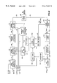
- state machine 300 which, based upon the current data and prior data, chooses the appropriate digital waveform recording stored in the PROM 310 according to the rules of bipolar coding.
- state machine 300 outputs a three bit address, A 8 -A 10 , which indicates the proper memory location in PROM 310 at which the desired digital waveform recording is stored.
- state machine 300 comprises three registers, which output the three bit address A 8 -A 10 , and some control and feedback logic. The control logic is designed such that it chooses the appropriate digital recording using the input data and the rules of bipolar coding.
- each digital waveform recording comprises 256 eight bit words.
- 8-bit counter 320 which outputs bits A 0 -A 7 , is used to clock the 256 eight bit words making up the digital waveform recording out of the PROM 310 as digital waveform signal 312 .
- the carry signal 322 of 8-bit counter 320 is sent to state machine 300 as an indication of when that the digital waveform recording has been completely output by PROM 310 .
- Clock 330 is set at 256 times the data rate and is input into state machine 300 , 8-bit counter 320 , and 8-bit video DAC 340 .
- a data clock signal 332 which is equal to the clock signal output from clock 330 divided by 256, is generated by state machine 300 and output to the CPU board (not shown) of the RFTT 6 to ensure that the data coming into state machine 300 is synchronous.
- digital waveform signal 312 output by PROM 310 is input into 8-bit video DAC 340 which converts digital waveform signal 312 into analog waveform signal 342 .
- the analog waveform signal 342 preferably has a frequency of 3.2 MHz.
- Analog waveform signal 342 is then passed through low pass filter 350 and up converter 360 which moves the signal to the preferred transmit frequency of 750 MHz, set the appropriate power level, and removes any alias or image frequencies.
- 750 MHz RF signal 95 is output to the HFC network where it is received by the UIUs 8 .
Abstract
Description
Claims (16)
Priority Applications (1)
| Application Number | Priority Date | Filing Date | Title |
|---|---|---|---|
| US09/413,271 US6172632B1 (en) | 1997-04-03 | 1999-10-06 | Bipolar FSK digital waveform synthesizer for modem systems |
Applications Claiming Priority (2)
| Application Number | Priority Date | Filing Date | Title |
|---|---|---|---|
| US08/826,630 US6282236B1 (en) | 1997-04-03 | 1997-04-03 | Modem designs, and systems using the modem designs for communicating information between a number of remote locations and one or more central locations |
| US09/413,271 US6172632B1 (en) | 1997-04-03 | 1999-10-06 | Bipolar FSK digital waveform synthesizer for modem systems |
Related Parent Applications (1)
| Application Number | Title | Priority Date | Filing Date |
|---|---|---|---|
| US08/826,630 Division US6282236B1 (en) | 1997-04-03 | 1997-04-03 | Modem designs, and systems using the modem designs for communicating information between a number of remote locations and one or more central locations |
Publications (1)
| Publication Number | Publication Date |
|---|---|
| US6172632B1 true US6172632B1 (en) | 2001-01-09 |
Family
ID=25247118
Family Applications (3)
| Application Number | Title | Priority Date | Filing Date |
|---|---|---|---|
| US08/826,630 Expired - Fee Related US6282236B1 (en) | 1997-04-03 | 1997-04-03 | Modem designs, and systems using the modem designs for communicating information between a number of remote locations and one or more central locations |
| US09/413,271 Expired - Lifetime US6172632B1 (en) | 1997-04-03 | 1999-10-06 | Bipolar FSK digital waveform synthesizer for modem systems |
| US09/413,833 Expired - Fee Related US6067325A (en) | 1997-04-03 | 1999-10-06 | Modem designs, and systems using the modem designs for communicating information between a number of remote locations and one or more central locations |
Family Applications Before (1)
| Application Number | Title | Priority Date | Filing Date |
|---|---|---|---|
| US08/826,630 Expired - Fee Related US6282236B1 (en) | 1997-04-03 | 1997-04-03 | Modem designs, and systems using the modem designs for communicating information between a number of remote locations and one or more central locations |
Family Applications After (1)
| Application Number | Title | Priority Date | Filing Date |
|---|---|---|---|
| US09/413,833 Expired - Fee Related US6067325A (en) | 1997-04-03 | 1999-10-06 | Modem designs, and systems using the modem designs for communicating information between a number of remote locations and one or more central locations |
Country Status (1)
| Country | Link |
|---|---|
| US (3) | US6282236B1 (en) |
Cited By (6)
| Publication number | Priority date | Publication date | Assignee | Title |
|---|---|---|---|---|
| US6567020B2 (en) * | 2000-08-30 | 2003-05-20 | Nokia Mobile Phones Ltd. | Method and arrangement for reducing interference |
| US20040081469A1 (en) * | 2002-10-28 | 2004-04-29 | Conway Joshua A. | Optical differential quadrature phase-shift keyed decoder |
| US20050048931A1 (en) * | 2003-09-02 | 2005-03-03 | Klaas Wortel | FSK modulator using IQ up-mixers and sinewave coded DACs |
| CN1326408C (en) * | 2003-03-12 | 2007-07-11 | 威盛电子股份有限公司 | Device for modnlating radio communication signal |
| CN100401639C (en) * | 2003-09-29 | 2008-07-09 | 苏州顺芯半导体有限公司 | Audio frequency D/A converter having variable lead and variable base pin use |
| WO2018148543A1 (en) * | 2017-02-10 | 2018-08-16 | Porter Carl Edmund | Apparatus and method for generating and capturing a transmission wave and apparatus and method for transmitting and receiving digital information |
Families Citing this family (6)
| Publication number | Priority date | Publication date | Assignee | Title |
|---|---|---|---|---|
| JP2000261380A (en) * | 1999-03-04 | 2000-09-22 | Sony Corp | System and method for optical communication |
| DE10297754B4 (en) * | 2002-06-24 | 2008-07-24 | Samsung Electronics Co., Ltd., Suwon | A memory module having a transmission path for high-speed data and a transmission path for low-speed data, memory system with such a memory module and method for transmitting data in such a memory module |
| CN100345127C (en) * | 2003-02-26 | 2007-10-24 | 厦门华侨电子股份有限公司 | Processing apparatus and method for converting high-speed serial data into parallel data |
| US20080052019A1 (en) * | 2006-08-25 | 2008-02-28 | Brennan W J | Compact Data Transmission Protocol for Electric Utility Meters |
| US9264282B2 (en) * | 2013-03-15 | 2016-02-16 | Innophase, Inc. | Polar receiver signal processing apparatus and methods |
| US9083588B1 (en) | 2013-03-15 | 2015-07-14 | Innophase, Inc. | Polar receiver with adjustable delay and signal processing metho |
Citations (4)
| Publication number | Priority date | Publication date | Assignee | Title |
|---|---|---|---|---|
| US4556869A (en) * | 1983-06-08 | 1985-12-03 | At&T Bell Laboratories | Multi-function data signal processing method and apparatus |
| US5237324A (en) * | 1991-09-04 | 1993-08-17 | Advanced Micro Devices, Inc. | System and method for producing baseband analog modulation signals |
| US5406584A (en) * | 1992-09-01 | 1995-04-11 | X-Com, Inc. | Time shift keying digital communications system |
| US6009465A (en) * | 1996-01-22 | 1999-12-28 | Svi Systems, Inc. | Entertainment and information systems and related management networks for a remote video delivery system |
Family Cites Families (9)
| Publication number | Priority date | Publication date | Assignee | Title |
|---|---|---|---|---|
| US4317220A (en) * | 1979-02-05 | 1982-02-23 | Andre Martin | Simulcast transmission system |
| GB2064271B (en) * | 1979-07-06 | 1983-09-28 | Plessey Co Ltd | Transceivers |
| JPS5625849A (en) * | 1979-08-10 | 1981-03-12 | Hitachi Ltd | Coding system |
| DE4202682A1 (en) * | 1992-01-31 | 1993-08-05 | Sel Alcatel Ag | PARALLEL ADDITIVE SCRAMBLER AND DESCRAMBLER |
| US5982645A (en) * | 1992-08-25 | 1999-11-09 | Square D Company | Power conversion and distribution system |
| US5247308A (en) * | 1993-02-24 | 1993-09-21 | The United States Of America As Represented By The Secretary Of The Army | Detection and characterization of LPI signals |
| US5535247A (en) * | 1993-09-24 | 1996-07-09 | Motorola, Inc. | Frequency modifier for a transmitter |
| JP2917890B2 (en) * | 1996-02-09 | 1999-07-12 | 日本電気株式会社 | Wireless transceiver |
| FI112133B (en) * | 1996-03-29 | 2003-10-31 | Nokia Corp | Method of forming the frequencies of a direct conversion transmitter / receiver operating in two different frequency ranges and a direct conversion transmitter / receiver of a radio communication system operating in two different frequency ranges and using the foregoing in a mobile telephone |
-
1997
- 1997-04-03 US US08/826,630 patent/US6282236B1/en not_active Expired - Fee Related
-
1999
- 1999-10-06 US US09/413,271 patent/US6172632B1/en not_active Expired - Lifetime
- 1999-10-06 US US09/413,833 patent/US6067325A/en not_active Expired - Fee Related
Patent Citations (4)
| Publication number | Priority date | Publication date | Assignee | Title |
|---|---|---|---|---|
| US4556869A (en) * | 1983-06-08 | 1985-12-03 | At&T Bell Laboratories | Multi-function data signal processing method and apparatus |
| US5237324A (en) * | 1991-09-04 | 1993-08-17 | Advanced Micro Devices, Inc. | System and method for producing baseband analog modulation signals |
| US5406584A (en) * | 1992-09-01 | 1995-04-11 | X-Com, Inc. | Time shift keying digital communications system |
| US6009465A (en) * | 1996-01-22 | 1999-12-28 | Svi Systems, Inc. | Entertainment and information systems and related management networks for a remote video delivery system |
Cited By (11)
| Publication number | Priority date | Publication date | Assignee | Title |
|---|---|---|---|---|
| US6567020B2 (en) * | 2000-08-30 | 2003-05-20 | Nokia Mobile Phones Ltd. | Method and arrangement for reducing interference |
| US20040081469A1 (en) * | 2002-10-28 | 2004-04-29 | Conway Joshua A. | Optical differential quadrature phase-shift keyed decoder |
| US7190908B2 (en) * | 2002-10-28 | 2007-03-13 | The Boeing Company | Optical differential quadrature phase-shift keyed decoder |
| CN1326408C (en) * | 2003-03-12 | 2007-07-11 | 威盛电子股份有限公司 | Device for modnlating radio communication signal |
| US20050048931A1 (en) * | 2003-09-02 | 2005-03-03 | Klaas Wortel | FSK modulator using IQ up-mixers and sinewave coded DACs |
| US7043222B2 (en) | 2003-09-02 | 2006-05-09 | Standard Microsystems Corporation | FSK modulator using IQ up-mixers and sinewave coded DACs |
| CN100401639C (en) * | 2003-09-29 | 2008-07-09 | 苏州顺芯半导体有限公司 | Audio frequency D/A converter having variable lead and variable base pin use |
| WO2018148543A1 (en) * | 2017-02-10 | 2018-08-16 | Porter Carl Edmund | Apparatus and method for generating and capturing a transmission wave and apparatus and method for transmitting and receiving digital information |
| US10804997B2 (en) | 2017-02-10 | 2020-10-13 | CTwists, LLC | Apparatus and method for generating and capturing a transmission wave and apparatus and method for transmitting and receiving digital information |
| US11342983B2 (en) | 2017-02-10 | 2022-05-24 | CTwists, LLC | Apparatus for transmitting digital information using electromagnetic waves, data transmission apparatus, and method |
| US11483056B2 (en) | 2017-02-10 | 2022-10-25 | CTwists, LLC | Apparatus and method of encoding information and symbols |
Also Published As
| Publication number | Publication date |
|---|---|
| US6282236B1 (en) | 2001-08-28 |
| US6067325A (en) | 2000-05-23 |
Similar Documents
| Publication | Publication Date | Title |
|---|---|---|
| US6693917B1 (en) | Digital subchannel transceiver for transmitting data | |
| CA2208460C (en) | Frequency synchronized bidirectional radio system | |
| US6172632B1 (en) | Bipolar FSK digital waveform synthesizer for modem systems | |
| US4742532A (en) | High speed binary data communication system | |
| US7103086B2 (en) | Frequency hopping data radio | |
| WO1996019875A9 (en) | Frequency synchronized bidirectional radio system | |
| MXPA04006127A (en) | Frequency hopping spread spectrum communications system. | |
| US6101214A (en) | Power line communications spread spectrum symbol timing and random phasing | |
| EP0620959A1 (en) | Frequency synchronized bidirectional radio system | |
| US6078630A (en) | Phase-based receiver with multiple sampling frequencies | |
| WO1996026576A1 (en) | Error detection in a wireless lan environment | |
| CA2011592A1 (en) | Multiple phase psk demodulator | |
| KR20070009710A (en) | Single and multiple sinewave modulation and demodulation techniques employing carrier-zero and carrier-peak data-word start and stop | |
| GB2070396A (en) | Transmission systems for transmitting signals over power distribution networks and transmitters for use therein | |
| JPS58130658A (en) | Modulator/demodulator set for digital communication | |
| US6236675B1 (en) | Pilot tone system and method to allow continuous synchronization in multipoint networks | |
| GB2148076A (en) | Microprocessor fsk data communications module | |
| US20020064218A1 (en) | Data link for multi protocol facility distributed communication hub | |
| US6684059B1 (en) | Frequency generation in a wireless communication system | |
| WO1996004740A1 (en) | Fsk permutation modulation | |
| TWI226172B (en) | Non-coherent FSK demodulator | |
| KR100518968B1 (en) | Power line communication modem | |
| Makhanov et al. | Noise immunity of radio and mobile communications | |
| KR200294000Y1 (en) | Power line communication modem | |
| Shapiro et al. | A full duplex 1200/300 bit/s single-chip CMOS model |
Legal Events
| Date | Code | Title | Description |
|---|---|---|---|
| FEPP | Fee payment procedure |
Free format text: PAYOR NUMBER ASSIGNED (ORIGINAL EVENT CODE: ASPN); ENTITY STATUS OF PATENT OWNER: LARGE ENTITY |
|
| STCF | Information on status: patent grant |
Free format text: PATENTED CASE |
|
| AS | Assignment |
Owner name: THE CHASE MANHATTAN BANK, AS COLLATERAL AGENT, TEX Free format text: CONDITIONAL ASSIGNMENT OF AND SECURITY INTEREST IN PATENT RIGHTS;ASSIGNOR:LUCENT TECHNOLOGIES INC. (DE CORPORATION);REEL/FRAME:011722/0048 Effective date: 20010222 |
|
| FPAY | Fee payment |
Year of fee payment: 4 |
|
| AS | Assignment |
Owner name: LUCENT TECHNOLOGIES INC., NEW JERSEY Free format text: TERMINATION AND RELEASE OF SECURITY INTEREST IN PATENT RIGHTS;ASSIGNOR:JPMORGAN CHASE BANK, N.A. (FORMERLY KNOWN AS THE CHASE MANHATTAN BANK), AS ADMINISTRATIVE AGENT;REEL/FRAME:018590/0287 Effective date: 20061130 |
|
| FEPP | Fee payment procedure |
Free format text: PAYER NUMBER DE-ASSIGNED (ORIGINAL EVENT CODE: RMPN); ENTITY STATUS OF PATENT OWNER: LARGE ENTITY Free format text: PAYOR NUMBER ASSIGNED (ORIGINAL EVENT CODE: ASPN); ENTITY STATUS OF PATENT OWNER: LARGE ENTITY |
|
| REMI | Maintenance fee reminder mailed | ||
| FPAY | Fee payment |
Year of fee payment: 8 |
|
| SULP | Surcharge for late payment |
Year of fee payment: 7 |
|
| FPAY | Fee payment |
Year of fee payment: 12 |
|
| AS | Assignment |
Owner name: 8631654 CANADA INC., CANADA Free format text: ASSIGNMENT OF ASSIGNORS INTEREST;ASSIGNOR:ALCATEL LUCENT S.A.;REEL/FRAME:031396/0262 Effective date: 20130913 |
|
| AS | Assignment |
Owner name: QUARTERHILL INC., CANADA Free format text: MERGER AND CHANGE OF NAME;ASSIGNORS:8631654 CANADA INC.;QUARTERHILL INC.;REEL/FRAME:043027/0098 Effective date: 20170601 |
|
| AS | Assignment |
Owner name: WI-LAN INC., CANADA Free format text: ASSIGNMENT OF ASSIGNORS INTEREST;ASSIGNOR:QUARTERHILL INC.;REEL/FRAME:043285/0115 Effective date: 20170601 |