US6173385B1 - Address generator for solid state disk drive - Google Patents

Address generator for solid state disk drive Download PDF

Info

Publication number
US6173385B1
US6173385B1 US08/155,332 US15533293A US6173385B1 US 6173385 B1 US6173385 B1 US 6173385B1 US 15533293 A US15533293 A US 15533293A US 6173385 B1 US6173385 B1 US 6173385B1
Authority
US
United States
Prior art keywords
address
logical block
block
bit
solid state
Prior art date
Legal status (The legal status is an assumption and is not a legal conclusion. Google has not performed a legal analysis and makes no representation as to the accuracy of the status listed.)
Expired - Fee Related
Application number
US08/155,332
Inventor
George B. Tuma
Wade B. Tuma
Current Assignee (The listed assignees may be inaccurate. Google has not performed a legal analysis and makes no representation or warranty as to the accuracy of the list.)
Database Excelleration Systems Inc
Original Assignee
Disk Emulation Systems Inc
Priority date (The priority date is an assumption and is not a legal conclusion. Google has not performed a legal analysis and makes no representation as to the accuracy of the date listed.)
Filing date
Publication date
Application filed by Disk Emulation Systems Inc filed Critical Disk Emulation Systems Inc
Priority to US08/155,332 priority Critical patent/US6173385B1/en
Assigned to DISK EMULATION SYSTEMS, INC. reassignment DISK EMULATION SYSTEMS, INC. ASSIGNMENT OF ASSIGNORS INTEREST (SEE DOCUMENT FOR DETAILS). Assignors: TUMA, GEORGE B., TUMA, WADE B.
Priority to CA002176148A priority patent/CA2176148C/en
Priority to AU10994/95A priority patent/AU1099495A/en
Priority to PCT/US1994/013301 priority patent/WO1995014272A1/en
Priority to EP95901939A priority patent/EP0729608A4/en
Assigned to DATABASE EXCELLERATION SYSTEMS, INC. reassignment DATABASE EXCELLERATION SYSTEMS, INC. ASSIGNMENT OF ASSIGNORS INTEREST (SEE DOCUMENT FOR DETAILS). Assignors: DISK EMULATION SYSTEMS, INC.
Priority to US08/641,934 priority patent/US6035384A/en
Publication of US6173385B1 publication Critical patent/US6173385B1/en
Application granted granted Critical
Assigned to ICP LLC, AS COLLATERAL AGENT reassignment ICP LLC, AS COLLATERAL AGENT SECURITY INTEREST (SEE DOCUMENT FOR DETAILS). Assignors: SOLID DATA SYSTEMS, INC.
Assigned to PACIFIC BUSINESS FUNDING, A DIVISION OF CUPERTINO NATIONAL BANK reassignment PACIFIC BUSINESS FUNDING, A DIVISION OF CUPERTINO NATIONAL BANK SECURITY INTEREST (SEE DOCUMENT FOR DETAILS). Assignors: SOLID DATA SYSTEMS, INC.
Anticipated expiration legal-status Critical
Expired - Fee Related legal-status Critical Current

Links

Images

Classifications

    • GPHYSICS
    • G06COMPUTING; CALCULATING OR COUNTING
    • G06FELECTRIC DIGITAL DATA PROCESSING
    • G06F3/00Input arrangements for transferring data to be processed into a form capable of being handled by the computer; Output arrangements for transferring data from processing unit to output unit, e.g. interface arrangements
    • G06F3/06Digital input from, or digital output to, record carriers, e.g. RAID, emulated record carriers or networked record carriers
    • G06F3/0601Interfaces specially adapted for storage systems
    • G06F3/0602Interfaces specially adapted for storage systems specifically adapted to achieve a particular effect
    • G06F3/061Improving I/O performance
    • G06F3/0613Improving I/O performance in relation to throughput
    • GPHYSICS
    • G06COMPUTING; CALCULATING OR COUNTING
    • G06FELECTRIC DIGITAL DATA PROCESSING
    • G06F3/00Input arrangements for transferring data to be processed into a form capable of being handled by the computer; Output arrangements for transferring data from processing unit to output unit, e.g. interface arrangements
    • G06F3/06Digital input from, or digital output to, record carriers, e.g. RAID, emulated record carriers or networked record carriers
    • G06F3/0601Interfaces specially adapted for storage systems
    • G06F3/0628Interfaces specially adapted for storage systems making use of a particular technique
    • G06F3/0638Organizing or formatting or addressing of data
    • G06F3/064Management of blocks
    • GPHYSICS
    • G06COMPUTING; CALCULATING OR COUNTING
    • G06FELECTRIC DIGITAL DATA PROCESSING
    • G06F3/00Input arrangements for transferring data to be processed into a form capable of being handled by the computer; Output arrangements for transferring data from processing unit to output unit, e.g. interface arrangements
    • G06F3/06Digital input from, or digital output to, record carriers, e.g. RAID, emulated record carriers or networked record carriers
    • G06F3/0601Interfaces specially adapted for storage systems
    • G06F3/0668Interfaces specially adapted for storage systems adopting a particular infrastructure
    • G06F3/0671In-line storage system
    • G06F3/0673Single storage device
    • G06F3/0679Non-volatile semiconductor memory device, e.g. flash memory, one time programmable memory [OTP]

Definitions

  • This disclosure includes a microfiche appendix having 1 fiche and a total of 35 frames.
  • This invention relates to address generators and more specifically to an address generator for a “solid state disk” which is a random access memory device which appears to a host computer system to be a disk drive.
  • SSDs Solid State Disks
  • SSDs based on contiguous random access (semiconductor) memory chips, can access the proper information based on the specified logical block.
  • An example of an SSD (which however is not block-length oriented) is disclosed in U.S. Pat. No. 5,070,474.
  • the SCSI host computer 10 presents the SSD 12 with a command to read or write along with the desired logical block and the number of blocks to be written or read on SCSI bus 14 .
  • the SSD controller 16 must interpret this command received from SCSI interface 18 and set the DRAM memory array 22 (DRAM chips) to the appropriate starting address via address generator 26 . This is analogous to the seek time in a rotating (physical) disk drive.
  • the controller 16 then reads or writes the proper number of blocks to the memory array 22 on address bus 24 . (Block-length oriented SSDs are known in the art.)
  • Address generator 26 operates in response to signal AGEN from controller 16 .
  • SSD 12 also conventionally includes DMA (direct memory address) controller 30 and error correction circuitry 32 connected by various busses as shown. Also included is a backup interface 34 and backup physical disk 38 .
  • DMA direct memory address
  • Block zero begins at an address of zero, block one begins 512 bytes later, block two at 1024 bytes and so on. Should a second system be based upon a block size of 256 bytes per block these addresses would change. In this case block zero would still begin at byte zero, but block one would occur at byte 256 , block two at byte 512 and so on.
  • the method for locating the desired starting address is:
  • the SCSI read/write extended commands specify the desired logical block as a 32 bit variable.
  • the logical block length is as large as 16 bits in a typical computer system. Normally this multiplication is performed in software in a microprocessor or microcontroller 16 using multiply functions or various shifting techniques. Such operations on variables of this magnitude can require many machine cycles on small (reasonably priced) microcontrollers. This results in long seek times which are undesirable in a solid state disk. Microcontrollers allowing 32 bit operations are expensive, difficult to embed and otherwise unnecessary for a typical SCSI peripheral.
  • the present invention in one embodiment includes a dedicated logic circuit for determining the desired starting address of an SSD operation (read or write).
  • the circuit is a multiplier circuit which, as data block numbers are received by the multiplier, multiplies the data block number by a block size value to quickly generate the address.
  • the block size value is (in one embodiment) programmed once, at power up of the SSD, with the appropriate value for the desired block size. (Alternatively the block size value is dynamically alterable after power up).
  • the access time is in the submicrosecond range for any typical block size.
  • FIG. 1 shows a solid state disk drive system diagram
  • FIG. 2 is a typical computer peripheral interface bus command packet.
  • FIG. 3 is a block diagram of an address generator in accordance with the invention.
  • FIG. 4 is a schematic diagram of an address generator in accordance with the present invention.
  • a SCSI peripheral is a block oriented device. Read or write operations specify a starting logical block, and the number of blocks to be written or read. The logical block size is selected by the host computer using a mode select command. The SCSI peripheral stores the logical block size in a non-volatile location. This logical block size remains valid until a subsequent mode select command modifies the block size again.
  • a SCSI SSD retrieves the appropriate size value for logical blocks.
  • the correct logical block size multiplication factor is then programmed into the address generation circuit in accordance with the invention.
  • Normal operation begins when the host computer system issues a read or write command to the SSD.
  • the SCSI interface logic receives the command and checks the validity of the command packet.
  • An example of a SCSI valid command packet is shown in FIG. 2 .
  • Bytes 02 to 05 specify the logical block at which the read operation is to begin.
  • the SCSI interface logic 18 signals the microprocessor 16 in the SSD that a valid command packet is present in the buffer of the SCSI interface logic 18 .
  • the microprocessor 16 then reads the command packet from the SCSI interface 18 buffer. If the command is determined to require reading or writing data, then the microprocessor 16 transfers the starting logical block information directly to the address generation circuit 26 .
  • FIG. 3 shows in a block diagram an address generation circuit 26 in accordance with the present invention.
  • the block number (which in this example is a 32 bit value) is received over an input bus 50 from a SCSI port (not shown).
  • bus 50 instead of being a 32 bit bus is an 8 bit bus, data on which is provided sequentially in four 8 bit bytes.
  • the block number is then received into a 32 bit set of latches 54 .
  • the latches 54 transmit their data to a shift register 58 having 32 bits.
  • a block size value is provided on an 8 bit bus 62 as an input data signal to a registered counter 66 which is an 8 bit device.
  • the input data signal is an 8 bit multiplication factor, not the actual block size, but derived therefrom as described below.
  • the registered counter 66 has a “load” terminal which responds to the AGEN* (address generation) signal transmitted from microprocessor 16 of FIG. 1 .
  • the registered counter 66 Upon receipt of the AGEN* signal, the registered counter 66 transmits the block size data value held in its register to a NAND gate 70 .
  • the second input to NAND gate 70 is a DCLK signal which is the system MEMORY clock signal.
  • NAND gate 70 triggers the shift register 58 to engage in shifts a number of times equal to the data value held in the registered counter 66 , when signal AGEN* is received.
  • the output of the registered counter 66 also is a clock signal to the 32 bit counter block 74 as shown via flip-flop 78 .
  • the values held in shift register 58 are transferred to the counter 74 which then transmits them out as a address on an address bus 24 to the random access memory array 22 of FIG. 1 .
  • FIG. 4 is a detailed schematic of one embodiment of address generator 26 .
  • Latches U 37 , U 38 , U 39 and U 40 store the start logical block information received on lines EXT DB [ 0 , . . . , 8 ] as clocked in by signals on lines E [ 2 , . . . , 5 ].
  • the microprocessor 16 negates signal AGEN* input to inverter U 114 B and then flip-flop U 41 A to begin the address generation cycle.
  • the address generation circuit includes also cascaded 4 bit shift registers U 18 , U 19 , U 20 , U 21 , U 22 , U 23 and U 24 which provide the basis for a 28 bit “hardware” (dedicated logic) multiplier circuit.
  • the exemplary associated SSD is of 2 gigabytes storage capacity using 4 MB DRAM chips in the memory array.
  • the memory array is 16 modules each containing 128 megabytes, thus 2 gigabytes total.
  • a 28 bit address bus is adequate; however, as DRAM chip density increases, the maximum memory array capacity and hence address bus may grow, e.g. to 32 bits.
  • One address generator is provided for each module.
  • the address data from the latches U 37 , . . . ,U 40 is loaded into the shift register string U 18 , . . . ,U 24 . Then every clock signal supplied to the shift registers U 18 , . . . ,U 24 on their CLK terminals multiplies the address data by two.
  • the shift register-multiplier U 18 , . . . ,U 24 will be clocked proportionally more times than for small block sizes.
  • the number of shift register clock signals is controlled by registered counter U 44 , which conventionally consists of an 8 bit register connected to a presettable 8 bit counter.
  • Signal lines E 0 thru E 15 are enables for various components in the microprocessor 16 external memory map.
  • the microprocessor 16 can read and/or write these locations across the system address bus (SAB).
  • the clock signal DCLK is e.g. a 16 MHZ clock source; thus each multiplication by two is accomplished in 62.5 nanoseconds.
  • Output buffers U 1 , U 2 , U 3 in turn drive resistor blocks RP 1 , RP 2 , RP 3 which drive address lines AL 0 , . . . , AL 10 , AH 0 , . . . , AH 10 and BS 0 , BS 1 .
  • Buffers U 1 , U 2 , and U 3 are required to drive the address lines on as many as 16 memory modules.
  • Counter U 5 drives demultiplexer U 15 .
  • the outputs of demultiplexer U 15 are the module select lines that select any one of the 16 memory modules.
  • OR gates U 45 A and U 45 B are part of the address decoding for location E 7 of the microprocessor 16 external memory map. Reading location E 7 allows the microprocessor 16 to determine which memory module is currently selected. This is accomplished through external buffer U 25 . Writing to location E 7 increments counter U 5 . This selects the next memory module. Input buffer U 43 increases the drive capacity of the CMOS microcontroller 16 .
  • Counter U 36 and comparator U 17 are part of a circuit that controls the switch from one memory module to the next. When a module switch is requested, the microprocessor 16 reads the current module number. If the module is not the last, then microprocessor 16 increments counter U 5 . If it is the last module, then the command is terminated with an overrange error condition.
  • Signal lines WR and RD carry the strobe signals from the microprocessor 16 that respectively read and write data to various other components.
  • SCRUB is a signal line that allows the memory array 22 to correct memory errors during the refresh cycles.
  • Lines DATA/REF ADR data refresh address
  • RFRQ fresh request
  • Counter U 122 counts the signals on line RFRQ and then supplies the count to multiplexer U 92 , the selection signal for which is supplied on line DATA/REF ADR; when the signal on DATA/REF ADR is low, refreshing is taking place.
  • the multiplication factor (logical block size value) is adjusted due to the nature of the registered counter U 44 used in this circuit.
  • the registered counter U 44 is an 8 bit device. This implies a count range from 0 to 255 with terminal carry at count 255.
  • the correct preset value for the register part of register-counter U 44 is therefore 255 minus the desired number of clocks.
  • the multiplier is the required number of clocks to be presented to the shift register, i.e., the multiplication factor.
  • the “register value” is the actual value supplied to registered counter U 44 .
  • a computer program resident in microprocessor 16 in the SSD is shown in the microfiche appendix; relevant portions of the program that control address generation are at line 390 and following showing the registered counter 390 being programmed; line 878 and following showing a real routine with AGEN at line 960 ; and at line 1031 and following showing a write routine with AGEN at line 1100 .
  • the program is in the 8051 assembly code language.
  • This computer program is copyrighted; the copyright owner gives permission for facsimile reproduction of material in Patent Office files, but reserves all other copyright rights.
  • the present invention in addition to being compatible with the SCSI interface, is also compatible with other computer bus peripheral interfaces such as IPI or DSSI or similar interfaces that are block specific. More generally, the present invention is applicable to any interface for computer systems which address memory using a logical block number and a block size, and in particular where the block size is of varying (programmable) length.

Abstract

An address generator for a solid state disk drive device includes a hardware multiplier logic circuit dedicated to computation of the address by multiplying a lock size by a logical block number, to obtain the start address for a memory array read or write operation. The dedicated multiplier circuit advantageously provides very quick computation of these relatively large numbers, which typically involves a 32 bit by 16 bit multiplication. The multiplier includes a shift register initially holding the logical block number which is shifted a particular number of times, the number of shift pulses representing a value of the block length. The output of the shift register is the desired address.

Description

MICROFICHE APPENDIX
This disclosure includes a microfiche appendix having 1 fiche and a total of 35 frames.
1. Field of the Invention
This invention relates to address generators and more specifically to an address generator for a “solid state disk” which is a random access memory device which appears to a host computer system to be a disk drive.
2. Description of the Prior Art
The well known SCSI interface is ideal for high performance solid state disks. Unlike ESDI or SMD interfaces, the SCSI interface presents the peripheral with the number of the desired logical block to be accessed. Solid State Disks (SSDs), based on contiguous random access (semiconductor) memory chips, can access the proper information based on the specified logical block. An example of an SSD (which however is not block-length oriented) is disclosed in U.S. Pat. No. 5,070,474.
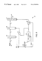
Referring to the system diagram in FIG. 1, the SCSI host computer 10 presents the SSD 12 with a command to read or write along with the desired logical block and the number of blocks to be written or read on SCSI bus 14. The SSD controller 16 must interpret this command received from SCSI interface 18 and set the DRAM memory array 22 (DRAM chips) to the appropriate starting address via address generator 26. This is analogous to the seek time in a rotating (physical) disk drive. The controller 16 then reads or writes the proper number of blocks to the memory array 22 on address bus 24. (Block-length oriented SSDs are known in the art.) Address generator 26 operates in response to signal AGEN from controller 16.
SSD 12 also conventionally includes DMA (direct memory address) controller 30 and error correction circuitry 32 connected by various busses as shown. Also included is a backup interface 34 and backup physical disk 38.
A difficulty arises due to the variable length of the logical blocks. Consider a typical host computer system 10 based on a logical block length of 512 bytes per block. Block zero begins at an address of zero, block one begins 512 bytes later, block two at 1024 bytes and so on. Should a second system be based upon a block size of 256 bytes per block these addresses would change. In this case block zero would still begin at byte zero, but block one would occur at byte 256, block two at byte 512 and so on.
The method for locating the desired starting address is:
Starting Address=Desired Logical Block×Logical Block Length
While the method is simple, the magnitude of the variables causes difficulty. The SCSI read/write extended commands specify the desired logical block as a 32 bit variable. The logical block length is as large as 16 bits in a typical computer system. Normally this multiplication is performed in software in a microprocessor or microcontroller 16 using multiply functions or various shifting techniques. Such operations on variables of this magnitude can require many machine cycles on small (reasonably priced) microcontrollers. This results in long seek times which are undesirable in a solid state disk. Microcontrollers allowing 32 bit operations are expensive, difficult to embed and otherwise unnecessary for a typical SCSI peripheral.
SUMMARY OF THE INVENTION
The present invention in one embodiment includes a dedicated logic circuit for determining the desired starting address of an SSD operation (read or write). The circuit is a multiplier circuit which, as data block numbers are received by the multiplier, multiplies the data block number by a block size value to quickly generate the address. The block size value is (in one embodiment) programmed once, at power up of the SSD, with the appropriate value for the desired block size. (Alternatively the block size value is dynamically alterable after power up). The access time is in the submicrosecond range for any typical block size.
In a typical SCSI application where a physical (not solid state) disk drive is used, the speed limit of the system is fairly low due to the relatively slow access time of a physical disk drive. The same is true for the relatively slow access time for tape drives and other types of rotating magnetic memory. Thus in these cases, there is no need for a higher speed address generator than that provided in the prior art software address generation calculation, and so use of a dedicated multiplier logic circuit in a physical disk drive address generator would not appear generally to be useful.
BRIEF DESCRIPTION OF THE DRAWINGS
FIG. 1 shows a solid state disk drive system diagram.
FIG. 2 is a typical computer peripheral interface bus command packet.
FIG. 3 is a block diagram of an address generator in accordance with the invention.
FIG. 4 is a schematic diagram of an address generator in accordance with the present invention.
DETAILED DESCRIPTION OF THE INVENTION
A SCSI peripheral is a block oriented device. Read or write operations specify a starting logical block, and the number of blocks to be written or read. The logical block size is selected by the host computer using a mode select command. The SCSI peripheral stores the logical block size in a non-volatile location. This logical block size remains valid until a subsequent mode select command modifies the block size again.
During the initial power up phase, a SCSI SSD retrieves the appropriate size value for logical blocks. The correct logical block size multiplication factor is then programmed into the address generation circuit in accordance with the invention.
Normal operation begins when the host computer system issues a read or write command to the SSD. The SCSI interface logic receives the command and checks the validity of the command packet. An example of a SCSI valid command packet is shown in FIG. 2. Bytes 02 to 05 specify the logical block at which the read operation is to begin. When the command has been determined valid, the SCSI interface logic 18 signals the microprocessor 16 in the SSD that a valid command packet is present in the buffer of the SCSI interface logic 18.
The microprocessor 16 then reads the command packet from the SCSI interface 18 buffer. If the command is determined to require reading or writing data, then the microprocessor 16 transfers the starting logical block information directly to the address generation circuit 26.
FIG. 3 shows in a block diagram an address generation circuit 26 in accordance with the present invention. The block number (which in this example is a 32 bit value) is received over an input bus 50 from a SCSI port (not shown). In one version bus 50 instead of being a 32 bit bus is an 8 bit bus, data on which is provided sequentially in four 8 bit bytes. The block number is then received into a 32 bit set of latches 54. In response to a clock signal CLK, the latches 54 transmit their data to a shift register 58 having 32 bits.
Separately, at power up of the address generation circuit 26, a block size value is provided on an 8 bit bus 62 as an input data signal to a registered counter 66 which is an 8 bit device. (In this case the input data signal is an 8 bit multiplication factor, not the actual block size, but derived therefrom as described below.) The registered counter 66 has a “load” terminal which responds to the AGEN* (address generation) signal transmitted from microprocessor 16 of FIG. 1. Upon receipt of the AGEN* signal, the registered counter 66 transmits the block size data value held in its register to a NAND gate 70. The second input to NAND gate 70 is a DCLK signal which is the system MEMORY clock signal. Thus, NAND gate 70 triggers the shift register 58 to engage in shifts a number of times equal to the data value held in the registered counter 66, when signal AGEN* is received. The output of the registered counter 66 also is a clock signal to the 32 bit counter block 74 as shown via flip-flop 78. The values held in shift register 58 are transferred to the counter 74 which then transmits them out as a address on an address bus 24 to the random access memory array 22 of FIG. 1.
FIG. 4 is a detailed schematic of one embodiment of address generator 26. Latches U37, U38, U39 and U40 store the start logical block information received on lines EXT DB [0, . . . , 8] as clocked in by signals on lines E [2, . . . , 5]. (Hence the start logical block number can be up to 32 bits=8 bits×4.) Immediately after, the microprocessor 16 (not shown) negates signal AGEN* input to inverter U114B and then flip-flop U41A to begin the address generation cycle.
The address generation circuit includes also cascaded 4 bit shift registers U18, U19, U20, U21, U22, U23 and U24 which provide the basis for a 28 bit “hardware” (dedicated logic) multiplier circuit. In this schematic the exemplary associated SSD is of 2 gigabytes storage capacity using 4 MB DRAM chips in the memory array. The memory array is 16 modules each containing 128 megabytes, thus 2 gigabytes total. Thus a 28 bit address bus is adequate; however, as DRAM chip density increases, the maximum memory array capacity and hence address bus may grow, e.g. to 32 bits. One address generator is provided for each module.
The address data from the latches U37, . . . ,U40 is loaded into the shift register string U18, . . . ,U24. Then every clock signal supplied to the shift registers U18, . . . ,U24 on their CLK terminals multiplies the address data by two. Thus for large block sizes the shift register-multiplier U18, . . . ,U24 will be clocked proportionally more times than for small block sizes.
The number of shift register clock signals is controlled by registered counter U44, which conventionally consists of an 8 bit register connected to a presettable 8 bit counter. The register is programmed on power up of the SSD with the appropriate multiplication factor on bus EXT DB [0, . . . , 8] for E=5. Signal lines E0 thru E15 are enables for various components in the microprocessor 16 external memory map. The microprocessor 16 can read and/or write these locations across the system address bus (SAB).
When signal AGEN* is set low by the microprocessor 16 of the SSD, the contents of the register part of U44 are loaded into the counter part of U44 because the CLOAD line (connected to the output terminal of flip-flop U41A) has gone low. This causes “ripple carry” to go high on the output terminal RCO of counter U44, and this signal propagates via flip-flop U42A through to the NAND gate U25B. This allows signal DCLK (provided to the second input terminal of NAND gate U25B) through NAND gate 25B, to clock the shift register string U18, . . . ,U24. Each DCLK signal thus multiplies the address data by two.
The clock signal DCLK is e.g. a 16 MHZ clock source; thus each multiplication by two is accomplished in 62.5 nanoseconds.
This multiplication process continues until the internal counter of counter U44 “rolls over” and sets its output signal ripple carry RCO low. This low signal propagates through flip-flop U42A and stops the clock signal to the shift register-multiplier U18, . . . ,U24. Finally this low signal propagates through flip-flop U42B and loads the multiplied address data (i.e., the start address) into the counter string consisting of counters U6, U7, U8, U9, U10 and U11 by clocking each of these counters. The 24 bit output signal of counters U6, . . . ,U11 are provided to the memory array as the starting address for reading or writing this particular logical block. (Only 24 address bits are needed in this particular embodiment.) Output buffers U1, U2, U3 in turn drive resistor blocks RP1, RP2, RP3 which drive address lines AL0, . . . , AL10, AH0, . . . , AH10 and BS0, BS1. Buffers U1, U2, and U3 are required to drive the address lines on as many as 16 memory modules.
Counter U5 drives demultiplexer U15. The outputs of demultiplexer U15 are the module select lines that select any one of the 16 memory modules. OR gates U45A and U45B are part of the address decoding for location E7 of the microprocessor 16 external memory map. Reading location E7 allows the microprocessor 16 to determine which memory module is currently selected. This is accomplished through external buffer U25. Writing to location E7 increments counter U5. This selects the next memory module. Input buffer U43 increases the drive capacity of the CMOS microcontroller 16. Counter U36 and comparator U17 are part of a circuit that controls the switch from one memory module to the next. When a module switch is requested, the microprocessor 16 reads the current module number. If the module is not the last, then microprocessor 16 increments counter U5. If it is the last module, then the command is terminated with an overrange error condition.
Signal lines WR and RD carry the strobe signals from the microprocessor 16 that respectively read and write data to various other components. SCRUB is a signal line that allows the memory array 22 to correct memory errors during the refresh cycles.
Lines DATA/REF ADR (data refresh address) and RFRQ (refresh request) carry signals that enable the address generator to support 4 MB DRAM chips in DRAM memory array 22. Counter U122 counts the signals on line RFRQ and then supplies the count to multiplexer U92, the selection signal for which is supplied on line DATA/REF ADR; when the signal on DATA/REF ADR is low, refreshing is taking place.
The multiplication factor (logical block size value) is adjusted due to the nature of the registered counter U44 used in this circuit. As previously mentioned, the registered counter U44 is an 8 bit device. This implies a count range from 0 to 255 with terminal carry at count 255. Each clock signal of the shift register is a multiply by two, so that one clock=2×, two clocks =4×, three clocks =8× etc. The correct preset value for the register part of register-counter U44 is therefore 255 minus the desired number of clocks.
Naively, it would seem that the desired multiplication factor would be directly the logical block size. Under these conditions, because 512 equals 29, the correct value for the register would be 255−9=246. This is correct if the memory array produces an output that is only one byte wide. However solid state disks can be implemented with a memory array that is considerably wider if single byte resolution is not necessary.
An exemplary solid state disk has a memory bus that is eight bytes wide. Eight equals 23, and therefore the correct block size value factor for this system would be 255−9+3=249, assuming a 512 byte logical block. This is implemented by a lookup table in the microprocessor 16. The multiplier is the required number of clocks to be presented to the shift register, i.e., the multiplication factor. The circuit stops the multiplication process at rollover, thus the “register value” =255−multiplier. The “register value” is the actual value supplied to registered counter U44.
Logical Block Size Multiplier Register Value
256 5 250
512 6 249
1024 7 248
2048 8 247
4096 9 246
A computer program resident in microprocessor 16 in the SSD is shown in the microfiche appendix; relevant portions of the program that control address generation are at line 390 and following showing the registered counter 390 being programmed; line 878 and following showing a real routine with AGEN at line 960; and at line 1031 and following showing a write routine with AGEN at line 1100. The program is in the 8051 assembly code language. This computer program is copyrighted; the copyright owner gives permission for facsimile reproduction of material in Patent Office files, but reserves all other copyright rights.
It is to be understood that the present invention, in addition to being compatible with the SCSI interface, is also compatible with other computer bus peripheral interfaces such as IPI or DSSI or similar interfaces that are block specific. More generally, the present invention is applicable to any interface for computer systems which address memory using a logical block number and a block size, and in particular where the block size is of varying (programmable) length.
The above description is illustrative and not limiting; further modifications will be apparent in light of this disclosure and are intended to be covered by the appended claims.

Claims (1)

We claim:
1. A method of generating an address for addressing a memory array, comprising:
receiving from a computer bus interface port a block number and a programmable block size value;
providing a multiplier circuit;
changing the block size value in response to a mode command;
multiplying the block number by the block size value in the multiplier circuit; and
providing the product of the step of multiplying from the multiplier circuit to the memory array as an address.
US08/155,332 1993-11-19 1993-11-19 Address generator for solid state disk drive Expired - Fee Related US6173385B1 (en)

Priority Applications (6)

Application Number Priority Date Filing Date Title
US08/155,332 US6173385B1 (en) 1993-11-19 1993-11-19 Address generator for solid state disk drive
EP95901939A EP0729608A4 (en) 1993-11-19 1994-11-18 Address generator for solid state disk drive
AU10994/95A AU1099495A (en) 1993-11-19 1994-11-18 Address generator for solid state disk drive
PCT/US1994/013301 WO1995014272A1 (en) 1993-11-19 1994-11-18 Address generator for solid state disk drive
CA002176148A CA2176148C (en) 1993-11-19 1994-11-18 Address generator for solid state disk drive
US08/641,934 US6035384A (en) 1993-11-19 1996-05-02 Solid state disk drive address generator with multiplier circuit

Applications Claiming Priority (1)

Application Number Priority Date Filing Date Title
US08/155,332 US6173385B1 (en) 1993-11-19 1993-11-19 Address generator for solid state disk drive

Related Child Applications (1)

Application Number Title Priority Date Filing Date
US08/641,934 Continuation US6035384A (en) 1993-11-19 1996-05-02 Solid state disk drive address generator with multiplier circuit

Publications (1)

Publication Number Publication Date
US6173385B1 true US6173385B1 (en) 2001-01-09

Family

ID=22555013

Family Applications (2)

Application Number Title Priority Date Filing Date
US08/155,332 Expired - Fee Related US6173385B1 (en) 1993-11-19 1993-11-19 Address generator for solid state disk drive
US08/641,934 Expired - Lifetime US6035384A (en) 1993-11-19 1996-05-02 Solid state disk drive address generator with multiplier circuit

Family Applications After (1)

Application Number Title Priority Date Filing Date
US08/641,934 Expired - Lifetime US6035384A (en) 1993-11-19 1996-05-02 Solid state disk drive address generator with multiplier circuit

Country Status (5)

Country Link
US (2) US6173385B1 (en)
EP (1) EP0729608A4 (en)
AU (1) AU1099495A (en)
CA (1) CA2176148C (en)
WO (1) WO1995014272A1 (en)

Cited By (8)

* Cited by examiner, † Cited by third party
Publication number Priority date Publication date Assignee Title
US20020093850A1 (en) * 2000-12-22 2002-07-18 Martin Hurich Interface for a memory, and method for variable configuration of a memory apparatus
US20040199753A1 (en) * 2003-03-31 2004-10-07 Sun Microsystems, Inc. Helper logic for complex instructions
US7028299B1 (en) * 2000-06-30 2006-04-11 Intel Corporation Task-based multiprocessing system
US20080263569A1 (en) * 2007-04-19 2008-10-23 Microsoft Corporation Composite solid state drive identification and optimization technologies
CN103034590A (en) * 2011-09-30 2013-04-10 国际商业机器公司 Method and system for direct memory address for solid-state drives
US20140156924A1 (en) * 2012-12-04 2014-06-05 SK Hynix Inc. Semiconductor memory device with improved operating speed and data storage device including the same
US9348518B2 (en) 2014-07-02 2016-05-24 International Business Machines Corporation Buffered automated flash controller connected directly to processor memory bus
US9542284B2 (en) 2014-08-06 2017-01-10 International Business Machines Corporation Buffered automated flash controller connected directly to processor memory bus

Families Citing this family (8)

* Cited by examiner, † Cited by third party
Publication number Priority date Publication date Assignee Title
GB2291991A (en) * 1995-09-27 1996-02-07 Memory Corp Plc Disk drive emulation with a block-erasable memory
US6233625B1 (en) * 1998-11-18 2001-05-15 Compaq Computer Corporation System and method for applying initialization power to SCSI devices
US20020039388A1 (en) * 2000-02-29 2002-04-04 Smart Kevin J. High data-rate powerline network system and method
US6981070B1 (en) * 2000-07-12 2005-12-27 Shun Hang Luk Network storage device having solid-state non-volatile memory
US6473355B2 (en) 2000-12-01 2002-10-29 Genatek, Inc. Apparatus for using volatile memory for long-term storage
US6742140B2 (en) 2000-12-01 2004-05-25 Jason R. Caulkins Method for using volatile memory for long-term storage
US9922696B1 (en) 2016-10-28 2018-03-20 Samsung Electronics Co., Ltd. Circuits and micro-architecture for a DRAM-based processing unit
US11017834B2 (en) * 2018-11-30 2021-05-25 Micron Technology, Inc. Refresh command management

Citations (5)

* Cited by examiner, † Cited by third party
Publication number Priority date Publication date Assignee Title
US5070474A (en) 1988-07-26 1991-12-03 Disk Emulation Systems, Inc. Disk emulation system
US5088031A (en) * 1985-02-20 1992-02-11 Hitachi, Ltd. Virtual machine file control system which translates block numbers into virtual addresses then into real addresses for accessing main storage
US5179662A (en) 1989-08-31 1993-01-12 International Business Machines Corporation Optimized i/o buffers having the ability to increase or decrease in size to meet system requirements
US5218691A (en) 1988-07-26 1993-06-08 Disk Emulation Systems, Inc. Disk emulation system
US5343426A (en) * 1992-06-11 1994-08-30 Digital Equipment Corporation Data formater/converter for use with solid-state disk memory using storage devices with defects

Family Cites Families (1)

* Cited by examiner, † Cited by third party
Publication number Priority date Publication date Assignee Title
US4819152A (en) * 1985-04-05 1989-04-04 Raytheon Company Method and apparatus for addressing a memory by array transformations

Patent Citations (5)

* Cited by examiner, † Cited by third party
Publication number Priority date Publication date Assignee Title
US5088031A (en) * 1985-02-20 1992-02-11 Hitachi, Ltd. Virtual machine file control system which translates block numbers into virtual addresses then into real addresses for accessing main storage
US5070474A (en) 1988-07-26 1991-12-03 Disk Emulation Systems, Inc. Disk emulation system
US5218691A (en) 1988-07-26 1993-06-08 Disk Emulation Systems, Inc. Disk emulation system
US5179662A (en) 1989-08-31 1993-01-12 International Business Machines Corporation Optimized i/o buffers having the ability to increase or decrease in size to meet system requirements
US5343426A (en) * 1992-06-11 1994-08-30 Digital Equipment Corporation Data formater/converter for use with solid-state disk memory using storage devices with defects

Cited By (20)

* Cited by examiner, † Cited by third party
Publication number Priority date Publication date Assignee Title
US7028299B1 (en) * 2000-06-30 2006-04-11 Intel Corporation Task-based multiprocessing system
US20020093850A1 (en) * 2000-12-22 2002-07-18 Martin Hurich Interface for a memory, and method for variable configuration of a memory apparatus
US6684291B2 (en) * 2000-12-22 2004-01-27 Robert Bosch Gmbh Interface for a memory, and method for variable configuration of a memory apparatus
US20040199753A1 (en) * 2003-03-31 2004-10-07 Sun Microsystems, Inc. Helper logic for complex instructions
US7219218B2 (en) * 2003-03-31 2007-05-15 Sun Microsystems, Inc. Vector technique for addressing helper instruction groups associated with complex instructions
US20080263569A1 (en) * 2007-04-19 2008-10-23 Microsoft Corporation Composite solid state drive identification and optimization technologies
US9940038B2 (en) 2007-04-19 2018-04-10 Microsoft Technology Licensing, Llc Composite solid state drive identification and optimization technologies
US8429677B2 (en) 2007-04-19 2013-04-23 Microsoft Corporation Composite solid state drive identification and optimization technologies
US9582415B2 (en) 2007-04-19 2017-02-28 Microsoft Technology Licensing, Llc Composite solid state drive identification and optimization technologies
US10564859B2 (en) 2007-04-19 2020-02-18 Microsoft Technology Licensing, Llc Composite solid state drive identification and optimization technologies
CN103034590A (en) * 2011-09-30 2013-04-10 国际商业机器公司 Method and system for direct memory address for solid-state drives
CN103034590B (en) * 2011-09-30 2015-09-16 国际商业机器公司 For the method and system of the direct memory addressing of solid-state drive
DE102012216034B4 (en) 2011-09-30 2021-11-25 International Business Machines Corporation Direct memory addressing for solid-state drives
US8683131B2 (en) 2011-09-30 2014-03-25 International Business Machines Corporation Direct memory address for solid-state drives
US8635407B2 (en) 2011-09-30 2014-01-21 International Business Machines Corporation Direct memory address for solid-state drives
US20140156924A1 (en) * 2012-12-04 2014-06-05 SK Hynix Inc. Semiconductor memory device with improved operating speed and data storage device including the same
US9852798B2 (en) 2014-07-02 2017-12-26 International Business Machines Corporation Buffered automated flash controller connected directly to processor memory bus
US10573392B2 (en) 2014-07-02 2020-02-25 International Business Machines Corporation Buffered automated flash controller connected directly to processor memory bus
US9348518B2 (en) 2014-07-02 2016-05-24 International Business Machines Corporation Buffered automated flash controller connected directly to processor memory bus
US9542284B2 (en) 2014-08-06 2017-01-10 International Business Machines Corporation Buffered automated flash controller connected directly to processor memory bus

Also Published As

Publication number Publication date
US6035384A (en) 2000-03-07
CA2176148C (en) 2002-01-22
AU1099495A (en) 1995-06-06
WO1995014272A1 (en) 1995-05-26
EP0729608A4 (en) 2001-04-18
EP0729608A1 (en) 1996-09-04
CA2176148A1 (en) 1995-05-26

Similar Documents

Publication Publication Date Title
US5394541A (en) Programmable memory timing method and apparatus for programmably generating generic and then type specific memory timing signals
US6173385B1 (en) Address generator for solid state disk drive
US6125072A (en) Method and apparatus for contiguously addressing a memory system having vertically expanded multiple memory arrays
US5265231A (en) Refresh control arrangement and a method for refreshing a plurality of random access memory banks in a memory system
US8667368B2 (en) Method and apparatus for reading NAND flash memory
US5754567A (en) Write reduction in flash memory systems through ECC usage
US5239639A (en) Efficient memory controller with an independent clock
US5920884A (en) Nonvolatile memory interface protocol which selects a memory device, transmits an address, deselects the device, subsequently reselects the device and accesses data
US5864568A (en) Semiconductor memory device for mass storage block access applications
US4532628A (en) System for periodically reading all memory locations to detect errors
US4359771A (en) Method and apparatus for testing and verifying the operation of error control apparatus within a memory
US20060195650A1 (en) Method to detect NAND-flash parameters by hardware automatically
US4369510A (en) Soft error rewrite control system
US6789179B2 (en) Method and system for fast data access using a memory array
US5621883A (en) Circuit for testing microprocessor memories
JPH04230544A (en) Data processing apparatus for dynamically setting timing of dynamic memory system
US7395398B2 (en) Memory controller that selectively changes frequency of a memory clock signal, a smart card including the same, and a method of controlling a read operation of a memory
US5765203A (en) Storage and addressing method for a buffer memory control system for accessing user and error imformation
US4625296A (en) Memory refresh circuit with varying system transparency
US11288014B2 (en) Controller, operating method of controller and storage device including the same
GB2367912A (en) Pattern generator for testing computer memory.
US5367526A (en) Memory module, parity bit emulator, and associated method for parity bit emulation
US6259651B1 (en) Method for generating a clock phase signal for controlling operation of a DRAM array
JPS6217783B2 (en)
US5915080A (en) Reprogramming device of a flash memory

Legal Events

Date Code Title Description
AS Assignment

Owner name: DISK EMULATION SYSTEMS, INC., NEVADA

Free format text: ASSIGNMENT OF ASSIGNORS INTEREST;ASSIGNORS:TUMA, GEORGE B.;TUMA, WADE B.;REEL/FRAME:006942/0922

Effective date: 19940315

AS Assignment

Owner name: DATABASE EXCELLERATION SYSTEMS, INC., CALIFORNIA

Free format text: ASSIGNMENT OF ASSIGNORS INTEREST;ASSIGNOR:DISK EMULATION SYSTEMS, INC.;REEL/FRAME:007656/0092

Effective date: 19950801

AS Assignment

Owner name: ICP LLC, AS COLLATERAL AGENT, CONNECTICUT

Free format text: SECURITY INTEREST;ASSIGNOR:SOLID DATA SYSTEMS, INC.;REEL/FRAME:011862/0172

Effective date: 20010810

AS Assignment

Owner name: PACIFIC BUSINESS FUNDING, A DIVISION OF CUPERTINO

Free format text: SECURITY INTEREST;ASSIGNOR:SOLID DATA SYSTEMS, INC.;REEL/FRAME:013727/0186

Effective date: 20020712

REMI Maintenance fee reminder mailed
LAPS Lapse for failure to pay maintenance fees
STCH Information on status: patent discontinuation

Free format text: PATENT EXPIRED DUE TO NONPAYMENT OF MAINTENANCE FEES UNDER 37 CFR 1.362

FP Lapsed due to failure to pay maintenance fee

Effective date: 20050109