US6173604B1 - Scanning evanescent electro-magnetic microscope - Google Patents
Scanning evanescent electro-magnetic microscope Download PDFInfo
- Publication number
- US6173604B1 US6173604B1 US09/158,037 US15803798A US6173604B1 US 6173604 B1 US6173604 B1 US 6173604B1 US 15803798 A US15803798 A US 15803798A US 6173604 B1 US6173604 B1 US 6173604B1
- Authority
- US
- United States
- Prior art keywords
- microscope
- tip
- sample
- frequency
- probe
- Prior art date
- Legal status (The legal status is an assumption and is not a legal conclusion. Google has not performed a legal analysis and makes no representation as to the accuracy of the status listed.)
- Expired - Lifetime
Links
Images


Classifications
-
- G—PHYSICS
- G01—MEASURING; TESTING
- G01Q—SCANNING-PROBE TECHNIQUES OR APPARATUS; APPLICATIONS OF SCANNING-PROBE TECHNIQUES, e.g. SCANNING PROBE MICROSCOPY [SPM]
- G01Q60/00—Particular types of SPM [Scanning Probe Microscopy] or microscopes; Essential components thereof
- G01Q60/18—SNOM [Scanning Near-Field Optical Microscopy] or apparatus therefor, e.g. SNOM probes
- G01Q60/22—Probes, their manufacture, or their related instrumentation, e.g. holders
-
- B—PERFORMING OPERATIONS; TRANSPORTING
- B82—NANOTECHNOLOGY
- B82Y—SPECIFIC USES OR APPLICATIONS OF NANOSTRUCTURES; MEASUREMENT OR ANALYSIS OF NANOSTRUCTURES; MANUFACTURE OR TREATMENT OF NANOSTRUCTURES
- B82Y20/00—Nanooptics, e.g. quantum optics or photonic crystals
-
- B—PERFORMING OPERATIONS; TRANSPORTING
- B82—NANOTECHNOLOGY
- B82Y—SPECIFIC USES OR APPLICATIONS OF NANOSTRUCTURES; MEASUREMENT OR ANALYSIS OF NANOSTRUCTURES; MANUFACTURE OR TREATMENT OF NANOSTRUCTURES
- B82Y35/00—Methods or apparatus for measurement or analysis of nanostructures
-
- Y—GENERAL TAGGING OF NEW TECHNOLOGICAL DEVELOPMENTS; GENERAL TAGGING OF CROSS-SECTIONAL TECHNOLOGIES SPANNING OVER SEVERAL SECTIONS OF THE IPC; TECHNICAL SUBJECTS COVERED BY FORMER USPC CROSS-REFERENCE ART COLLECTIONS [XRACs] AND DIGESTS
- Y10—TECHNICAL SUBJECTS COVERED BY FORMER USPC
- Y10S—TECHNICAL SUBJECTS COVERED BY FORMER USPC CROSS-REFERENCE ART COLLECTIONS [XRACs] AND DIGESTS
- Y10S977/00—Nanotechnology
- Y10S977/84—Manufacture, treatment, or detection of nanostructure
- Y10S977/849—Manufacture, treatment, or detection of nanostructure with scanning probe
- Y10S977/86—Scanning probe structure
- Y10S977/864—Electrostatic force probe
-
- Y—GENERAL TAGGING OF NEW TECHNOLOGICAL DEVELOPMENTS; GENERAL TAGGING OF CROSS-SECTIONAL TECHNOLOGIES SPANNING OVER SEVERAL SECTIONS OF THE IPC; TECHNICAL SUBJECTS COVERED BY FORMER USPC CROSS-REFERENCE ART COLLECTIONS [XRACs] AND DIGESTS
- Y10—TECHNICAL SUBJECTS COVERED BY FORMER USPC
- Y10S—TECHNICAL SUBJECTS COVERED BY FORMER USPC CROSS-REFERENCE ART COLLECTIONS [XRACs] AND DIGESTS
- Y10S977/00—Nanotechnology
- Y10S977/84—Manufacture, treatment, or detection of nanostructure
- Y10S977/849—Manufacture, treatment, or detection of nanostructure with scanning probe
- Y10S977/86—Scanning probe structure
- Y10S977/865—Magnetic force probe
-
- Y—GENERAL TAGGING OF NEW TECHNOLOGICAL DEVELOPMENTS; GENERAL TAGGING OF CROSS-SECTIONAL TECHNOLOGIES SPANNING OVER SEVERAL SECTIONS OF THE IPC; TECHNICAL SUBJECTS COVERED BY FORMER USPC CROSS-REFERENCE ART COLLECTIONS [XRACs] AND DIGESTS
- Y10—TECHNICAL SUBJECTS COVERED BY FORMER USPC
- Y10S—TECHNICAL SUBJECTS COVERED BY FORMER USPC CROSS-REFERENCE ART COLLECTIONS [XRACs] AND DIGESTS
- Y10S977/00—Nanotechnology
- Y10S977/84—Manufacture, treatment, or detection of nanostructure
- Y10S977/849—Manufacture, treatment, or detection of nanostructure with scanning probe
- Y10S977/86—Scanning probe structure
- Y10S977/868—Scanning probe structure with optical means
- Y10S977/869—Optical microscope
Definitions
- This invention relates generally to scanning probe microscopy and more specifically to scanning evanescent near field microwave and electromagnetic spectroscopy.
- Scanning probe type microscopes have typically been used to create visual images of a sample material.
- the image obtained may reflect any of a number of distinct electrical or magnetic properties of the sample material, depending on the parameter measured by the probe tip.
- the tip may image electron tunneling, atomic force, absorption and refraction of propagating or evanescent electromagnetic waves, or other parameters.
- the tip may be in contact with the sample or it may be a short distance above the sample.
- SPMs Scanning Probe Microscopes
- microscopy signals as obtained from SPMs often are a combined function of topography and physical properties of the material. Separating them requires measuring at least two independent signals.
- the tunneling current is a function of both the tip to sample distance and the density of states.
- a recently developed scanning near-field optical microscope can measure optical signals such as luminescent spectra or optical index of refraction in addition to shear force, which can be used to determine the distance between tip and sample.
- the invention comprises a near field scanning evanescent-wave microscope wherein a probe tip primarily emits an evanescent wave and wherein interfering propagating wave emissions are minimized. Propagating waves have low resolution while evanescent waves have high resolution. This feature is crucial for quantitative measurements, where only the near-field evanescent wave is modeled.
- a high resolution image is generated by scanning a sample with a novel evanescent wave probe on the inventive microscope.
- the inventive microscope provides complex electrical impedance values that are calculated from measured data and which are associated with the resolved image features.
- the complex impedance, including dielectric constant, loss tangent and conductivity can be measured for materials having properties that range from insulators to superconductors.
- the inventive microscope is capable of quantitative measurements of dielectric properties and surface resistance with submicron resolution.
- the resonance frequency (f r ) and quality factor (Q) of a resonant coaxial cavity coupled to the tip the electrical properties of the sample are measured.
- One embodiment of the SEMM comprises a ⁇ /4 coaxial resonator operating at frequency (f r ) of roughly 1 GHZ coupled to a sharp tip protruding from a narrow hole.
- f r and Q shift.
- the inventive microscope is capable of converting the measured f r and Q shifts to electrical parameters of the sample. Since the extremely small tip radius determines the extent of the field distribution, this microscope is capable of submicron resolution.
- the interaction between the probe tip and the sample is dependent on the dielectric constant and tangent loss of the nearby sample.
- the interaction depends on the surface resistance of the sample.
- the probe itself comprising either a resonator or a conventional coaxial body, is a key inventive feature of the microscope.
- An important novel feature of the probe tip is a conducting endwall having an aperture, through which the center conducting element of the coaxial cable or resonator extends without shorting to the endwall.
- Another key feature of the inventive microscope is the computing element programmed to convert measured changes in resonant frequency (or reflected electromagnetic wave) and measured changes in the quality factor to quantitative electrical parameters of the sample.
- An additional important feature of the inventive microscope is a means to maintain a constant separation distance between the tip and the sample while measurement scans of the sample are performed.
- FIG. 1 is a diagrammatic view of the various components which comprise the imaging evanescent near field microscope system.
- FIG. 2 is a diagrammatic view of the various components which comprise the quantitative evanescent near field microscope system.
- FIG. 2A is an enlarged detail view along lines 2 A— 2 A in FIG. 2 .
- FIG. 3 shows the image charge distribution for a thick sample in contact with the end of the probe tip.
- the q n series represents the charge redistribution on the tip;
- the q n ′ series represents the effect of polarization of the dielectric sample;
- the q n ′′ is the effective value of q n inside the sample.
- FIG. 4 shows the image charge distribution for the configuration with an air gap between a thick sample and the end of the probe tip. Symbols q n , q n ′, and q n ′′ have the same meaning as in FIG. 3 .
- FIG. 5 shows a graph of measured and fitted resonant frequency as a function of the distance between the end of the probe tip and the sample for a MgO single crystal.
- FIG. 6 shows distribution of image charges for a tip-sample configuration in which the sample comprises a thin film ( ⁇ 2 ) on a thick substrate ( ⁇ 1 ) and in which there is an air gap (g) between the probe tip and the film surfaces.
- Symbols q n , q n ′, and q n ′′ have the same meaning as in FIG. 3 .
- the q n ′ series represents the effect of polarization of the dielectric film induced by the field of the tip.
- the q n ′′ series represents the reaction on the film from the polarized substrate.
- the q n ′′′′ series represents the reaction on the tip form the polarized substrate
- the q n ′′′′′ series represents the polarization of the dielectric film caused by q n ′′′, etc.
- FIG. 7 shows the intrinsic spatial resolution, in units of tip radius, R 0 , of the SEMM as a function of dielectric constant.
- FIG. 8 shows the multiple image charge analysis of tip-sample interaction between the end of the probe tip and a conducting sample.
- FIG. 9 shows the magnetic field distribution on the surface of a conducting material surrounding the proximity of the probe tip.
- FIG. 10 shows the radial distribution for the magnetic field on the surface of a conducting material surrounding the proximity of the probe tip, for different probe tip radii, a 0 .
- FIG. 11 shows measured data points (triangles) and a best fit calculated curve from SEMM signals as a function of gap size between the probe tip and a copper sample using the resonant frequency equation 12.
- FIG. 12 shows measured data points (triangles) and a best fit calculated curve from SEMM signals as a function of gap size between the probe tip and a copper sample using the quality factor equation 19.
- FIG. 13 shows the spatial frequency spectra of the magnetic field on the surface of a conducting material for five different values of a 0 .
- FIG. 14 shows the power dissipated, S, in a conducting sample as a function of a 0 , the ratio of the gap distance to the radius of the probe tip.
- FIG. 15 shows on the left, a topographic image of a LiNb0 3 sample having periodically poled domains.
- the image on the right is of a simultaneously obtained first harmonic image in which the contribution from sample-probe geometry has been excluded.
- FIG. 16 shows an embodiment of the inventive probe tip comprising a coaxial cable instead of a resonator.
- FIG. 17 shows a change in frequency as a function of gap distance for a known metal, the curve being useful as a calibration curve for the gap distance controller.
- FIG. 18 shows results obtained using the SEMM to image conducting silver sections having differing heights but constant conductivity.
- FIG. 19 shows results obtained using the SEMM to image conducting metal sections having differing heights and differing conductivity.
- the electromagnetic frequency of the inventive microscope is limited on the high end by the electron mobility in the sample being measured (that is the plasma frequency of the material) and on the low end by the practicality of the physical dimension of the resonant cavity portion of the probe tip.
- frequencies ranging from the infrared region of the electromagnetic spectrum to the microwave region can be used on the scanning evanescent wave microscope. If the resonation is replaced by a coaxial cable having an end wall connected to the coaxial shielding element, the low end of the measurement frequency is essentially d.c.
- the evanescent-waves in this context refer to electromagnetic waves with wave-vectors of imaginary number not originating from dissipation.
- the evanescent electromagnetic waves are the photon equivalent of quantum mechanic electron waves in the classically forbidden region (within a barrier).
- an orthogonal eigenfunction set of Hilbert space is chosen as the plane waves whose wave vectors are any real number satisfying Helmholtz equation (as a consequence, these plane waves are propagating waves).
- Any propagating wave (for example, a propagating spherical wave from a point source) can be expanded as the superposition of these plane waves.
- These waves only have resolving power on the order of ⁇ .
- these plane waves can not be used to reconstruct, for example, a spherical wave whose wave front has a radius less than the wavelength ⁇ .
- a true complete set of Hilbert space should include plane waves whose wave-vectors are any complex number satisfying the Maxwell equation to construct such a spherical wave. Since imaginary wave vectors are allowed, the components (k x , k y , and k z ) can then be any value and still satisfy the Maxwell equation.
- these waves are “evanescent” and can not propagate much more than a wavelength ( ⁇ ).
- evanescent-wave microscopy uses different means to obtain strong evanescent waves and strong interaction between the evanescent wave and the substance under inspection.
- a metal sphere or tip fed by a wave source with a radius of r ( ⁇ ) will generate evanescent waves (to form a spherical wave on the metal surface satisfying the boundary conditions) whose wave vectors range up to k r ⁇ 1/r and resolving power up to ⁇ r.
- Interaction between the tip and sample may further increase the high k r components and resolution as a result of decreasing the effective tip radius from a polarizing effect.
- these waves decay over a distance (r) in free space, the sample has to be brought to within r of the tip to obtain strong interaction.
- FIG. 1 shows the inventive near field microscope system utilizing the novel evanescent probe structure comprising a microwave resonator such as illustrated microwave cavity 10 having generator 30 electrically connected to cavity 10 to feed an input signal, through a coaxial line 32 , into a coupled loop input 12 on cavity 10 .
- a coupled loop output 14 of cavity 10 is connected to a detector 40 through a second coaxial line 42 .
- Detector 40 feeds the output signal to a data acquisition unit 50 .
- the data from data acquisition unit 50 is then fed into a computer 60 which converts the data into an image viewable at image display 70 connected to computer 60 .
- One of the best prior art probe tips comprised an open-ended coaxial cable which included a center conducting wire surrounded by an insulator and enclosed in an external shield.
- This type of tip generates both a near-field evanescent wave, which doesn't propagate more than a few wavelengths ( ⁇ ) before it attenuates and thus results in high resolution measurements, and a far-field propagating wave.
- the propagating wave is undesirable because it interferes with the near-field evanescent wave.
- researchers attempted to use coaxial cables having smaller and smaller diameters, but eventually large energy loss and difficult physical construction to avoid electrical breakdown between the shield and center wire became a problem.
- the present inventors developed a configuration in which the center wire was sharpened and extended a distance beyond the shielding, or a sharpened tip was mechanically and electrically connected to the center wire.
- An additional inventive shielding element was added to the bottom edge of the coaxial cable in order to minimize any electromagnetic fields created between the sharpened end of the probe and the end of the external shielding, which when left open can allow far-field propagating wave to reach the sample and dominate the near-field evanescent wave.
- the present inventors added a resonator which was located immediately above or near the probe tip so that evanescent waves could be generated and sensed with greater efficiency and sensitivity, although the resonator is not a necessary component for every application.
- the inventive SEMM tip limits the creation of propagating waves so that high resolution evanescent wave measurements can be made effectively.
- One feature of the inventive tip that limits creation of far-field propagating waves is a conductive shielding element that extends over the portion of the coaxial cable that otherwise would have been open. Referring to FIGS. 1, 2 and 2 A at the end from which the probe tip 20 extends, a new electrically conducting shielding element 16 is located so that its outer edge connects to the exterior coaxial shield 17 and its inner edge circles, or surrounds, the probe tip without electrically shorting to it.
- the conducting shielding element 17 is preferably thin, on the order of 1 ⁇ m, to avoid causing excess loss. It is preferably physically supported by a low loss insulator like sapphire.
- the outer shield 17 is brought around the end portion 16 of the insulator but has an opening, or aperture 22 through which the probe can extend without electrically shorting to the shield.
- the aperture is conveniently circular but does not have to be circular.
- the aperture is smaller than either the coaxial cable or a resonator that is used to generate the evanescent wave.
- the end portion of the insulator forms a plane that is approximately normal to the line of the probe portion, however a tapered surface could span part of the distance between the outer shield and probe as long as the sensitivity of the probe remains acceptable and degradation of the Q factor is avoided.
- the Q factor is a function of the geometry of the cavity and tapering the walls of the cavity may lower it (as well as lowering the sensitivity) unacceptably for any given desired measurement.
- Q 2 ⁇ E total /E dissipated .
- Microwave generator 30 , detector 40 , image diode detector 34 , amplifier, phase shifter, A/D converter, data acquisition unit 50 , computer 60 , display 70 , movable target mount 90 , and X-Y-Z scanning control 100 all comprise commercially available equipment.
- microwave generator 30 is available from the Programmed Test Source Company as model PTS1000
- detector 40 is available from Pasternack Enterprises as model PE800-50
- data acquisition unit 50 is available from National Instruments as model PC-TIO02150
- computer 60 may comprise any standard programmable computer
- display 70 may comprise any commercially available monitor
- movable target mount or stepper mechanism 90 is available from the Ealing Company as model 61-0303.
- Design principles for a quarter wave cavity, such as cavity 10 may be found in “Radio Engineer Handbook” by F. E. Terman.
- Metal probe tip 20 has a sharpened end thereon which may be as fine as about 100 Angstroms in diameter
- the sharpened end of tip 20 will usually vary in diameter from as small as about 100 Angstrom 10 nm) to as large as about 100 ⁇ m, and preferably ranges from about 200 Angstroms (20 nm) to about 20 ⁇ m.
- Sharpened metal probe tip 20 may be formed, for example, by electrochemically etching one section of a wire which might have an initial diameter of from about 1 ⁇ m to about 0.2 millimeters (mm) prior to the electrochemical etch.
- Sharpened metal probe tip 20 may be connected to tapered end 19 of central conductor 18 by welding or any other suitable means which will provide a secure mechanical and electrical connection between tip 20 and tapered probe end 19 .
- the minimum diameter of aperture 22 has been determined to be the minimum diameter which maintains the high Q and sensitivity of the resonator.
- the aperture opening must be small enough that a propagating wave is not emitted that will interfere with the evanescent wave measurement.
- the minimum diameter of aperture 22 should be greater than the thickness of endwall 16 . That is, endwall thickness (t) divided by aperture diameter (d) must be much less than unity (t/d ⁇ 1) to maintain high Q (or low loss) of the resonator.
- the endwall should be made by plating a good conducting film (silver or copper) of about 1-2 ⁇ m thick on a low loss insulating plate ( ⁇ 1 mm thick), such as sapphire or LaA1O3 to reduce the thickness (t) while maintaining rigidity (mechanical vibration is not desired).
- the aperture diameter is also related to the diameter of the metal probe tip which passes through and beyond aperture 22 .
- the minimum aperture diameter therefore, will usually be at least about 200 Angstroms (20 nm). If the diameter of aperture 22 is too large, however, the resolution will be reduced. It has been found, however, that the diameter of aperture 22 may be as large as 3 mm while still maintaining satisfactory resolution.
- the diameter of aperture 22 will range from about 500 Angstroms (50 nm) to about 1 mm.
- a sharpened metal probe tip 20 extends through and beyond cylindrical aperture 22 in endwall 16 of resonator 10 .
- the reason why probe tip 20 must extend beyond aperture 22 a distance comparable to the diameter of aperture 22 , in accordance with the invention, is to reduce the effect of the size of the aperture on the resolution. That is, the reason probe tip 20 extends through and beyond aperture 22 , instead of terminating at aperture 22 , as in prior art structure, is to provide increased spatial resolution, dependent dimensionally on the radius of probe tip 20 rather than the diameter of aperture 22 .
- the extension of probe tip 20 beyond aperture 22 also is helpful and convenient for the scanning of the sample.
- the length of the portion of sharpened metal probe tip 20 which extends through and beyond aperture 22 is related to the diameter of aperture 22 .
- This length of probe tip 20 extending through and beyond aperture 22 will range from about 1 ⁇ 3 of the diameter of aperture 22 to about three times the diameter of aperture 22 .
- the preferred ratio of extension length to aperture diameter has been found to be about one.
- the extension length should be further selected to be the length that does not give rise to a large background signal (caused by radiation from the aperture which interacts with the sample) while still giving rise to a strong signal by the tip-sample interaction.
- a cavity 10 including shielding 32 and endwall 16 , is formed of metal but preferably comprises a diamagnetic material such as copper or silver, rather than a ferromagnetic material, so that a modulating magnetic field can be used in connection with cavity 10 .
- the cavity diameter should be large enough and the diameter ratio of cavity 10 to central electrode 18 should be about 3.6 to provide an optimum Q.
- the Q of a microwave cavity or resonator may be defined as the quality factor of the cavity, and should be kept as high as possible.
- the sensitivity of the near field microscope can be improved by increasing the input microwave power and unloaded Q, denoted Q u , of the resonator with an optimal coupling which is achieved by adjusting the coupling strength so that the loaded Q, denoted Q l , is 2/3 of Q u .
- the resonator cavity volume is filled with a dielectric material, preferably one having low loss.
- the relative dielectric constant is proportional to the dielectric constant of a vacuum.
- Sample dielectric materials that can be advantageously used to fill the resonator cavity include air, strontium titanate (SrTiO 3 ), and sapphire (Al 2 O 3 ).
- the resonator height is in integral multiples of ⁇ /4, that is n ⁇ /4 where n is an integer. If the resonator is an open resonator, n is an even integer; if the resonator is closed, n is an odd integer.
- FIG. 16 shows an embodiment of the inventive probe tip using a conventional coaxial cable in place of a resonator.
- An electromagnetic energy source 30 delivers electromagnetic energy to the cable.
- the coaxial cable has an outer electric shielding element 52 that surrounds an insulator element 44 and a central conducting element 48 .
- the central conducting element extends beyond the end of the coaxial cable and is either sharpened into a tip or a fine sharp tip is attached to it.
- a thin metal endwall 46 is attached to the insulator that is interposed between the shielding 52 and the center conductor 48 .
- the endwall thickness is guided by the same consideration as for the conductive endwall 16 at the end of the resonator.
- the endwall 46 located at the end of the coaxial cable, has an orifice of sufficient size to allow the center cable 48 to pass through it without electrically shorting the center probe to the endwall.
- the inventive probe comprising a coaxial cable, additionally has a directional coupler 43 located between the endwall 46 and the source 30 .
- the directional coupler 42 couples the source electromagnetic wave to the cable.
- the electromagnetic wave propagates down the cable to the end and is reflected back by the end wall. Interaction between the probe tip 54 and the sample being scanned modifies the properties of the reflected wave.
- the reflected wave is coupled to a detector 40 by directional coupler 43 and the amplitude and phase of the reflected wave are measured by the detector.
- Quantitative values of the physical properties of the sample such as complex conductivity, dielectric constant, tangent loss, conductivity, and other electrical parameters are determined using equations programmed into the SEMM.
- dielectric materials have been imaged having a spatial resolution of 100 nm and sensitivity of 1 ⁇ 10 ⁇ 3 . Furthermore, using a computation of an analytic expression of the field distribution around the probe tip, a quantitative measurement was taken of the complex electrical impedance dielectric material. Thus, a map of electrical impedance values was constructed that matched resolution and sensitivity of the image, and wherein the measured complex electrical impedance values were correlated to features visualized on the image.
- the coaxial resonator has a height of ⁇ /4.
- a sapphire disk 21 with a center hole only slightly larger than that of the tip wire was located in the end plate.
- the tip diameter was between about 50 ⁇ m and about 100 ⁇ m.
- a metal layer of about 1 ⁇ m was coated on the outside surface of the sapphire disk to shield the tip from far-field propagating components. The metal coating thickness is determined by the skin-depth to avoid the formation of a micro-transmission line, which would have heavy loss near the aperture.
- the sapphire disk serves to minimize vibration and is bonded to the probe tip using insulating glue.
- insulating glue having low energy loss may be used to fix the tip wire with respect to the endwall shielding so that the tip does not vibrate against the shielding.
- the entire resonant cavity is filled with a dielectric material such as SrTi0 3 .
- the height of the resonant cavity is greatly reduced as the resonant wavelength is inversely proportional to the square root of the relative dielectric constant of the material that fills the cavity.
- ⁇ is about 1.73 cm
- ⁇ /4 the height of the resonator, is only about 0.43 cm.
- the resonant diameter may shrink significantly also.
- an image is obtained by placing the tip of the resonator in direct physical contact with the sample to be imaged, and scanning the tip across the surface of the sample.
- the resonator is driven at a frequency that is slightly higher or lower than the resonant frequency of the resonator.
- the change in the resonant frequency is then measure by recording the output power at the input frequency (measured as the detector output voltage).
- the resonant frequency of the resonator is reduced as a function of the relative conductivity of different regions of the sample.
- very fine niobium wires coated on, say, silicon dioxide can be successfully imaged to a spatial resolution of about 5 ⁇ m (about ⁇ /100,000).
- a quantitative measurement is obtained of the complex electrical impedance.
- the resonant frequency, f r , and the quality factor, Q shifts as functions of the dielectric constant and loss tangent of any material, such as the sample material, located near the probe tip.
- this functional relationship was not well enough known, however, to obtain quantitative information about the dielectric constant, loss tangent, or complex electrical impedance, from a measured shifts in f r or Q.
- the present invention comprises a scanning evanescent wave resonant-probe microscope having a computing element capable of correctly relating a series of measured shifts in f r and Q to the complex electrical impedance, (e.g. dielectric constant, loss tangent, or conductivity) at a series of locations on the sample surface.
- the computing element is programmed to calculate values of ⁇ and tangent losses (tan ⁇ ) at a series of different frequencies.
- one method of measuring a dielectric constant and loss tangent of a sample comprises,
- the frequency versus power curve in the procedure above can be determined using a Lorentz line type fit to obtain f 0 , and Q 0 .
- the electromagnetic wave can be treated as quasi-static, that is, the wave nature of the field can be ignored.
- the sample material in the vicinity of the small probe tip is reasonably considered as homogeneous and isotropic in its dielectric properties.
- ⁇ ⁇ ′+j ⁇ ′′ where ⁇ is >> ⁇ 0 , and ⁇ ′>> ⁇ ′′, where ⁇ is the complex dielectric constant, ⁇ ′ is the real component of the dielectric constant, ⁇ ′′ is imaginary component of the dielectric constant, and ⁇ 0 is the dielectric constant of free space.
- ⁇ ⁇ ′+j ⁇ ′′ and ⁇ ⁇ 0 ;
- ⁇ is the complex magnetic permeability of the sample;
- ⁇ ′ is the real component of the magnetic permeability, and
- ⁇ ′′ is the imaginary component of the magnetic permeability, and
- ⁇ 0 is the magnetic permeability of free space.
- FIG. 3 shows a diagram of the measurement geometry.
- the probe tip 20 is in soft contact with the surface of a dielectric material 80 having a thickness much larger than the tip radius.
- the sample thickness may be more than two times as thick as the tip radius. More preferably it is five times as thick.
- the probe tip is represented as a charged conducting sphere under the same potential as the end point or tip of the center conductor in the endwall of the resonator, since the tip only extends out a length several orders of magnitude smaller than the wavelength beyond the cavity.
- the dielectric sample under the tip is polarized by the electric field of the tip and thus acts electrically on the tip causing a redistribution of charges on the tip to maintain the equipotential surface of the conducting sphere.
- the action on the tip is represented by an image charge (q 1 ′) located in the sample; the redistribution of charge in the probe tip is represented by another image charge (q 2 ) inside the spherically modeled tip end.
- This action and redistribution repeats itself, that is, it is iterative until equilibrium is attained.
- Three series of image point charges are formed that meet the boundary conditions at both tip and dielectric sample surfaces as shown in FIG. 3 .
- the peak value of the field distribution inside the sample can be expressed as a superposition of contributions from the series of point charges (q n ′′) the effective value of q n in the sample.
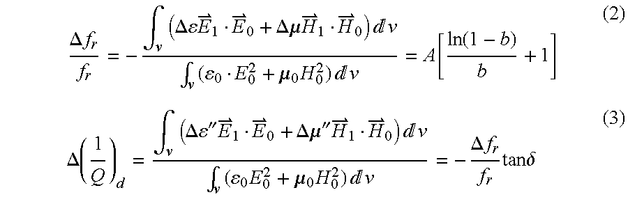
- perturbation theory for electromagnetic resonators where the frequency is perturbed slightly to find the resonant frequency or the amplitude of the energy deposited in the cavity is perturbed, can be used to calculate the f r and Q shifts that would result from a particular dielectric material, as noted in equations (2) and (3).
- E 0 , H 0 , and E 1 , H 1 refer to the electric and magnetic field before and after the perturbation, respectively
- ⁇ is the wavelength
- V 0 is the voltage on the probe tip.
- equation (2) shows that the shift in resonant frequency is proportional to the radius (R 0 ) of the probe tip. This is because the electric field near a conducting sphere, which is how the probe tip is modeled, at a given voltage is inversely proportional to the sphere radius and the total contribution to the signal is the integration of the square of the electrical field magnitude divided by the volume of the sample.
- the tan ⁇ is referred to as the loss tangent.
- the sample thickness may be at least about two times as thick as the probe tip radius. Preferably, the sample thickness is at least five times as thick as the probe tip radius. Even more preferably the sample thickness is at least ten times greater than the probe tip radius.
- the constants A and B are found by calibration against a standard sample such as sapphire that has a known dielectric constant and loss tangent. Table I lists relative dielectric constants ( ⁇ r ) and loss tangents for a number of materials measured using the inventive SEMM. The relative dielectric constants are relative to measurements taken in a vacuum or air.
- MgO Magnesium Oxide
- a′ which equals g/R 0 .
- One application of the inventive SEMM is measuring the dielectric constant of thin films.
- many films traditionally considered thin films would interact with the inventive probe as a bulk sample because of the extreme sharpness with which the probe tip can be made.
- the penetration depth of the field is calculated using equation 1 to be about the same as the radius of the probe tip, R 0 .
- Table II shows the results of measuring dielectric constants for thin films using the inventive SEMM and a conventional inter-digital contact electrode at 1 GHZ.
- Intrinsic spatial resolution is an important figure of merit for microscopes.
- the intrinsic resolution of the inventive microscope was estimated using equation 2 to calculate numerically the contribution to ( ⁇ f r /f r ) from small vertical columns as a function of lateral location (r) relative to the center of the tip for materials of different dielectric constants. The contribution was shown to decrease quickly as r increased, especially when ⁇ was large.
- the radius where the contribution from the volume inside the radius r reached 50% of the total contribution was defined as the intrinsic spatial resolution.
- the estimated resolution was about two orders of magnitude smaller than the tip radius at the moderate Er ( ⁇ 50) and decreased slightly as ⁇ r increased. This is illustrated in FIG. 7 .
- V 0 is the open end peak voltage.
- N Q u /(Q u ⁇ Q c ) is the insertion loss
- k B Bolzmann's constant
- B the bandwidth of the data acquisition.
- the classical skin-depth concept of conducting materials can be shown as no longer valid in describing the interaction between evanescent electromagnetic waves and conducting materials.
- the classical skin-depth concept is derived from the interaction between a conducting surface and propagating plane waves whose k vector components (k r , k z ) must be smaller than k 0 .
- k c >>k 0
- the inventive SEMM is based on a high quality factor (Q) microwave coaxial resonator with a sharpened metal tip mounted on the center conductor.
- the tip extends beyond an aperture formed on a thin metal shielding end-wall of the resonator.
- the tip and the shielding structure are designed so that the propagating far-field components are shielded within the cavity whereas the non-propagating evanescent waves are generated at the tip. This feature is crucial for both high resolution and quantitative analysis. Because it is not mathematically feasible to model the interactions of both evanescent and propagating waves, (where the latter are leaked from the resonator), quantitative microscopy would not be possible without the inventive microscope configuration.
- measurements of the conductivity of electrically conducting samples comprises the following steps:
- ⁇ 0 and ⁇ 0 are the permittivity and permeability of free space
- R 0 is the tip radius
- ⁇ overscore (e) ⁇ r and ⁇ overscore (e) ⁇ I are the unit vectors along the directions of the cylindrical coordinates r and z
- a n R 0 and q n are the position and charge of the nth image inside the tip, respectively.
- the typical ⁇ overscore (H) ⁇ field intensity profile obtained from equation 10 forms the shape of a volcano.
- the radial distributions for different tip-sample distances are depicted in FIG. 10 .
- the figure indicates that the size of caster (a measure of spatial resolution of the microscope) decreases and the intensity of the field increases with decreasing tip-sample distance, respectively.
- the inventors analyze the system through an equivalent series RLC circuit of the resonator.
- the tip is represented as a small capacitor, C′, whose capacitance depends on the tip-sample interaction, parallel to the main capacitor of the resonant circuit.
- the relative resonant frequency shift is then proportional to the variation of C′.
- the second order approximation and subsequently the refraction of evanescent electromagnetic wave on the surface of conducting materials and the decay behavior inside the materials must be considered.
- the inventors will first discuss the refraction of evanescent electromagnetic waves on the surface of conducting materials. Then, the wave decay and dissipation inside the conducting materials are computed to derive the conductivity quantitatively from the SEMM signals.
- H ⁇ s ⁇ ( k 0 ⁇ r ) 1 2 ⁇ ⁇ H ⁇ s ⁇ ( r ⁇ ) ⁇ exp ⁇ ( i ⁇ ⁇ k ⁇ 0 ⁇ r ⁇ r ⁇ ) ⁇ ⁇ s ( 14 )
- the calculated spatial frequency spectra for different ratios of tip-sample distances to tip radius (a 0 ) are shown in FIG. 12 . It is clear that a cut-off spatial frequency exists for certain R 0 and a 0 . It is also clear from the figure that the smaller the tip-sample distance (i.e. smaller the a 0 /R 0 ) is, the more intense the high spatial frequency components are. Also found in FIG. 12 is that the increase of the intensity with respect to the decrease of a 0 is very rapid in the high k 0r range and quite slow in the low k 0r range of the spectra. In other words, the field intensity increase associated with the decrease of the tip-sample distance is mainly concentrated in the high spatial frequency region.
- the inventors have developed a scanning evanescent electromagnetic microscope (SEMM) capable of quantitative measurements of dielectric properties and surface resistance with submicron resolution.
- SEMM scanning evanescent electromagnetic microscope
- the inventors measure the dielectric properties of the sample.
- the shift in f r corresponds to the dielectric constant of the material ( ⁇ ) while the shift in Q corresponds to the tangent loss (tan ⁇ ).
- the inventors estimate the local ⁇ and tan ⁇ . Since the tip radius determines the extent of the field distribution, this microscope is capable of submicron resolution.
- a constant tip-sample separation can be maintained by adjusting the tip-sample separation to maintain a constant f r in the cavity.
- the ability to perform non-contact imaging of the surface resistance opens up a variety of possible applications.
- a quantitative, analytic model for the tip-response for dielectric and metallic material was developed. Since the SEMM operates in the extreme near-field region, with resolution ⁇ /10 6 , the quasi-static approximation can be employed. The local electrical properties were estimated by modeling the tip as a metallic sphere and calculating a series of image charges. Quantitative modeling of the SEMM response was performed in the cases of metals and insulator. Quantitative comparisons of the tip response with the modeled response have been conducted as a function of distance and sample properties and have demonstrated accuracy within 5% on sample of widely varying dielectric and metallic properties.
- the frequency response can be measured.
- the theoretical curve can be fit and R 0 and the absolute separation at a given f r may be extracted. (FIG. 17)
- a frequency f RF is chosen to correspond to some tip-sample separation.
- a phase-locked loop is employed, where connection 31 on FIG. 2 is open.
- a constant RF frequency f RF is input into the cavity and the cavity output is mixed with a signal coming from a reference path.
- the length of the reference path is adjusted so that the output of the mixer is zero when f r matches f RF .
- the output of the phase detector is fed to an integrator, which regulates the tip-sample distance by changing the extension of a piezoelectric actuator (Burleigh PZS-050) to maintain the integrator output near zero.
- FIG. 18 To demonstrate the ability to separate topographic and electrical information, the inventors imaged a set of metallic squares of varying height on a metallic film (FIG. 18 ). This sample consists of 100 nm, 200 nm, and 400 nm Ag squares on a 2.1 ⁇ m Ag substrate on a sapphire substrate. They were 250 ⁇ m by 250 ⁇ m and separated by a distance of 60 ⁇ m. The topographic image shows clear variations in height for the different squares. The loss image is essentially featureless.
- FIG. 19 To demonstrate the ability to image surface resistance, the inventors imaged squares of varying resistivity (FIG. 19 ). This sample consists of Mn, Cr, and Zr squares deposited on 75 mn Pt on a silicon substrate. The variations in the topographic image correspond to real variations in height as measured by a profilometer. The variations in the loss image are clearly visible and correspond to variations in resistivity.
- the tip-sample distance (d) can be controlled by adjusting the distance to maintain a constant frequency shift.
- the inventors have implemented a feedback loop using a phase-sensitive detector to force a piezoelectric actuator (Burleigh PZS-050) to maintain a constant f r . For samples exhibiting a uniform frequency shift, this corresponds to a constant tip-sample separation.
- Sample topography is measured by monitoring the variation in voltage applied to the actuator. By simultaneous measurement of an additional signal, variations in sample properties can be imaged in conjunction with topography. Variations in the transmitted power correspond to variations in tangent loss or surface resistance.
- the first order nonlinear dielectric constant ( ⁇ ijk ) can also be measured.
- FIG. 15 This image was taken of a periodically poled single-crystal LiNbO 3 wafer. The topographic image is essentially featureless, with the exception of a constant tilt. The nonlinear image features a reversal in phase by the reversal of polarization in the alternating domains.
- Apertureless reflectance-mode near-field optical microscopy can also be used for distance regulation of a SEMM.
- the variation of material properties at optical frequencies is less than the variation at lower frequencies, making apertureless NSOM suitable for distance regulation.
- ‘Conventional’ near-field optics relies on the use of a tapered waveguide geometries of transmission or absorption. This waveguide can either confine or sample light from a region near an aperture with size smaller than the wavelength of light. This form of near-field optics requires the fabrication of a complex probe.
- apertureless NSOM a sharp, optically conducting tip is moved close to the sample and a highly focused spot illuminates the tip-sample region.
- apertureless NSOMs in which the tip was illuminated from below.
- These apertureless NSOMs are limited to use on optically transparent samples.
- the scattered light varies with the tip-sample separation and may be used for distance control, either by measurement of the amplitude or of the polarization of the scattered light.
- the inventors propose the use of a Schwartzchild lens, where a dark central region reduces the scattered background.
- a vertical dither may be used to reduce the effects of a far-field background. This dither should enable the detection of only that component of the optical signal that varies over small length scales. This method allows for control of the tip-sample separation in an SEMM with high resolution over a broad range of substrates in combination with simultaneous measurements of the sample's electrical properties.
- the tip-sample distance may also be regulated by differential measurement of the frequency shift. Vibrating the sample position, for example by placing a piezoelectric element under the sample, causes a change in resonance frequency and its harmonics. These changes are measured using, for example, a lock-in amplifier.
- the changes in resonance frequency will have sharper distance dependence than the microscope signal and can be used for distance control.
- the variation of f r at the frequency of the cavity dither will vary inversely with an additional factor of the tip-sample separation. If this vertical dither is small by comparison to the tip-sample separation, the total variation in acquired signal will be small, permitting simultaneous measurement of topography and the sample properties.
- the frequency shift and harmonic intensity are independent functions of the dielectric constant and the tip-sample distance, g, and give raise to two independent equations:
- Equation 5 Equation 5
- Equation 5 is then solved for f r and used as equation 20.
- Equation 21 is the first derivative taken with respect to g. The equations 20 and 21 are solved simultaneously to yield the dielectric constant, ⁇ , and the gap distance, g.
Abstract
Description


| TABLE I |
| Measured Dielectric Constants and Tangent Losses for Single Crystals |
| Measured | Reported | Measured | ||
| Material | εr | εr | tgδ | Reported tgδ |
| YSZ | 30.0 | 29 | 1.7 × 10⁻³ | 1.75 × 10⁻³ |
| LaGaO3 | 23.2 | 25 | 1.5 × 10⁻³ | 1.80 × 10⁻³ |
| CaNdAlO4 | 18.2 | 19.5 | 1.5 × 10⁻³ | 0.4-2.5 × 10⁻³ |
| TiO2 | 86.8 | 85 | 3.9 × 10⁻³ | 4 × 10⁻³ |
| BaTiO3 | 295 | 300 | 0.47 | 0.47 |
| YAlO3 | 16.8 | 16 | — | 8.2 |
| SrLaAlO4 | 18.9 | 20 | ||
| LaALO3 | 25.7 | 24 | 2.1 × 10⁻⁵ | |
| MgO | 9.5 | 9.8 | 1.6 × 10⁻⁵ | |
| LiNbO3(X-cut) | 32.0 | 30 | ||


| TABLE II |
| Measured dielectric constants and tangent losses of various thin films |
| By SEMM and interdigital electrode technique, both measured at 1 GHZ. |
| SEMM measurement | Interdigital electrodes |
| Films | ερ | tanδ | ερ | tanδ |
| SrTiO3 | 292 | 0.01 | 297 | 0.01 |
| Ba0.5Sr0.5TiO3 | 888 | 0.19 | 868 | 0.10 |
| Ba0.7Sr0.3TiO3 | 707 | 0.14 | 727 | 0.07 |


Claims (15)


Priority Applications (6)
| Application Number | Priority Date | Filing Date | Title |
|---|---|---|---|
| US09/158,037 US6173604B1 (en) | 1996-09-20 | 1998-09-22 | Scanning evanescent electro-magnetic microscope |
| TW87117103A TW396271B (en) | 1998-09-22 | 1998-10-15 | Scanning evanescent electro-magnetic microscope |
| US09/608,311 US7550963B1 (en) | 1996-09-20 | 2000-06-30 | Analytical scanning evanescent microwave microscope and control stage |
| US09/695,508 US6532806B1 (en) | 1996-09-20 | 2000-10-23 | Scanning evanescent electro-magnetic microscope |
| US11/454,171 US20060231756A1 (en) | 1996-09-20 | 2006-06-14 | Analytical scanning evanescent microwave microscope and control stage |
| US12/465,022 US8358141B2 (en) | 1996-09-20 | 2009-05-13 | Analytical scanning evanescent microwave microscope and control stage |
Applications Claiming Priority (2)
| Application Number | Priority Date | Filing Date | Title |
|---|---|---|---|
| US08/717,321 US5821410A (en) | 1996-09-20 | 1996-09-20 | Scanning tip microwave near field microscope |
| US09/158,037 US6173604B1 (en) | 1996-09-20 | 1998-09-22 | Scanning evanescent electro-magnetic microscope |
Related Parent Applications (1)
| Application Number | Title | Priority Date | Filing Date |
|---|---|---|---|
| US08/717,321 Continuation-In-Part US5821410A (en) | 1996-09-20 | 1996-09-20 | Scanning tip microwave near field microscope |
Related Child Applications (3)
| Application Number | Title | Priority Date | Filing Date |
|---|---|---|---|
| US09/608,311 Continuation-In-Part US7550963B1 (en) | 1996-09-20 | 2000-06-30 | Analytical scanning evanescent microwave microscope and control stage |
| US09/695,508 Division US6532806B1 (en) | 1996-09-20 | 2000-10-23 | Scanning evanescent electro-magnetic microscope |
| US11/454,171 Continuation-In-Part US20060231756A1 (en) | 1996-09-20 | 2006-06-14 | Analytical scanning evanescent microwave microscope and control stage |
Publications (1)
| Publication Number | Publication Date |
|---|---|
| US6173604B1 true US6173604B1 (en) | 2001-01-16 |
Family
ID=46203445
Family Applications (2)
| Application Number | Title | Priority Date | Filing Date |
|---|---|---|---|
| US09/158,037 Expired - Lifetime US6173604B1 (en) | 1996-09-20 | 1998-09-22 | Scanning evanescent electro-magnetic microscope |
| US09/695,508 Expired - Fee Related US6532806B1 (en) | 1996-09-20 | 2000-10-23 | Scanning evanescent electro-magnetic microscope |
Family Applications After (1)
| Application Number | Title | Priority Date | Filing Date |
|---|---|---|---|
| US09/695,508 Expired - Fee Related US6532806B1 (en) | 1996-09-20 | 2000-10-23 | Scanning evanescent electro-magnetic microscope |
Country Status (1)
| Country | Link |
|---|---|
| US (2) | US6173604B1 (en) |
Cited By (65)
| Publication number | Priority date | Publication date | Assignee | Title |
|---|---|---|---|---|
| US6274396B1 (en) * | 2001-01-29 | 2001-08-14 | Advanced Micro Devices, Inc. | Method of manufacturing calibration wafers for determining in-line defect scan tool sensitivity |
| US6422741B2 (en) * | 1994-04-11 | 2002-07-23 | The Johns Hopkins University | Method for nondestructive/noncontact microwave detection of electrical and magnetic property discontinuities in materials |
| US6525808B1 (en) * | 1998-12-04 | 2003-02-25 | University Of Cincinnati | Method and system for local index measurement in optical materials |
| US6532806B1 (en) | 1996-09-20 | 2003-03-18 | The Regents Of The University Of California | Scanning evanescent electro-magnetic microscope |
| US6597185B1 (en) | 2000-09-20 | 2003-07-22 | Neocera, Inc. | Apparatus for localized measurements of complex permittivity of a material |
| WO2003060462A2 (en) * | 2002-01-04 | 2003-07-24 | Dune Medical Devices Ltd. | Examining tissue according to dielectric properties thereof |
| US20030138378A1 (en) * | 2001-11-19 | 2003-07-24 | Dune Medical Devices Ltd. | Method and apparatus for examining tissue for predefined target cells, particularly cancerous cells, and a probe useful in such method and apparatus |
| US20030155934A1 (en) * | 2000-09-20 | 2003-08-21 | Moreland Robert L. | Apertured probes for localized measurements of a material's complex permittivity and fabrication method |
| US6614227B2 (en) * | 2000-12-04 | 2003-09-02 | Nec Corporation | Scanning microwave microscope capable of realizing high resolution and microwave resonator |
| US20030167831A1 (en) * | 2001-11-28 | 2003-09-11 | General Nanotechnology Llc | Method and apparatus for micromachines, microstructures, nanomachines and nanostructures |
| US6630825B2 (en) | 2001-08-23 | 2003-10-07 | Lake Shore Cryotronics, Inc. | Electromechanical drive for magnetometers |
| US6633660B1 (en) * | 1999-02-05 | 2003-10-14 | John Carl Schotland | Near-field tomography |
| US20040004484A1 (en) * | 2000-09-20 | 2004-01-08 | Talanov Vladimir V. | System and method for quantitative measurements of a material's complex permittivity with use of near-field microwave probes |
| DE10259118A1 (en) * | 2002-06-28 | 2004-05-19 | Fuchs, Harald, Prof. Dr. | Scanning probe microscopy is based on detection and spectral analysis of natural thermal electromagnetic near fields on surface |
| US6752008B1 (en) | 2001-03-08 | 2004-06-22 | General Nanotechnology Llc | Method and apparatus for scanning in scanning probe microscopy and presenting results |
| US20040118192A1 (en) * | 2002-09-09 | 2004-06-24 | General Nanotechnology Llc | Fluid delivery for scanning probe microscopy |
| WO2004057355A1 (en) * | 2002-12-20 | 2004-07-08 | The Provost Fellows And Scholars Of The College Of The Holy And Undivided Trinity Of Queen Elizabeth Near Dublin | A method and apparatus for inspection of high frequency and microwave hybrid circuits and printed circuit boards |
| US6787768B1 (en) | 2001-03-08 | 2004-09-07 | General Nanotechnology Llc | Method and apparatus for tool and tip design for nanomachining and measurement |
| US20040196037A1 (en) * | 2001-10-25 | 2004-10-07 | Intematix Corporation | Detection with evanescent wave probe |
| US6802646B1 (en) | 2001-04-30 | 2004-10-12 | General Nanotechnology Llc | Low-friction moving interfaces in micromachines and nanomachines |
| WO2004088668A2 (en) * | 2003-03-31 | 2004-10-14 | Siemens Aktiengesellschaft | Device and method for determining an electrical property of a sample |
| US6809533B1 (en) * | 1999-09-10 | 2004-10-26 | University Of Maryland, College Park | Quantitative imaging of dielectric permittivity and tunability |
| DE10314560A1 (en) * | 2003-03-31 | 2004-11-04 | Siemens Ag | Device and method for determining an electrical property of a sample |
| US20040226351A1 (en) * | 2003-05-16 | 2004-11-18 | Schafrik Robert E. | Non-destructive evaluation of thermal barrier coatings in gas turbine engines |
| US20040227525A1 (en) * | 2003-05-16 | 2004-11-18 | Hazel Brian Thomas | Non-destructive determination of machining induced surface defects on metal parts |
| US6861648B2 (en) | 1994-07-28 | 2005-03-01 | General Nanotechnology Llc | Scanning probe microscopy inspection and modification system |
| US20050056783A1 (en) * | 1999-07-01 | 2005-03-17 | General Nanotechnology, Llc | Object inspection and/or modification system and method |
| US20050115047A1 (en) * | 2001-01-30 | 2005-06-02 | General Nanotechnology Llc | Manufacturing of micro-objects such as miniature diamond tool tips |
| US20050190684A1 (en) * | 1995-07-24 | 2005-09-01 | General Nanotechnology Llc | Nanometer scale data storage device and associated positioning system |
| US6946835B1 (en) * | 2002-02-09 | 2005-09-20 | Intematix Corporation | Spatially resolved spin resonance detection |
| US20050230619A1 (en) * | 2004-04-09 | 2005-10-20 | Talanov Vladimir V | Method and system for measurement of dielectric constant of thin films using a near field microwave probe |
| US20060125465A1 (en) * | 2004-07-12 | 2006-06-15 | Xiao-Dong Xiang | Evanescent microwave probe with enhanced resolution and sensitivity |
| US20060160136A1 (en) * | 2004-12-08 | 2006-07-20 | Xiao-Dong Xiang | High throughput screening of catalysts using spin resonance |
| US20060174384A1 (en) * | 2001-10-19 | 2006-08-03 | Rave Llc | Scan data collection for better overall data accurancy |
| US20060237639A1 (en) * | 1994-07-28 | 2006-10-26 | General Nanotechnology Llc | Scanning probe microscope assembly and method for making spectrophotometric, near-filed, and scanning probe measurements |
| US20060253107A1 (en) * | 2004-03-23 | 2006-11-09 | Dune Medical Devices Ltd. | Clean margin assessment tool |
| US20060264738A1 (en) * | 2003-07-24 | 2006-11-23 | Dune Medical Devices Ltd. | Method and apparatus for examining a substance, particularly tissue, to characterize its type |
| US20060273794A1 (en) * | 2005-06-07 | 2006-12-07 | Carlos Meriles | Method and apparatus for high resolution nuclear magnetic resonance imaging and spectroscopy |
| US20070012093A1 (en) * | 2005-07-12 | 2007-01-18 | Psia Co, Ltd | Scanning capacitance microscope, method of driving the same, and recording medium storing program for implementing the method |
| US20070032739A1 (en) * | 2005-08-04 | 2007-02-08 | Dune Medical Devices Ltd. | Device for forming an effective sensor-to-tissue contact |
| US20070032747A1 (en) * | 2005-08-04 | 2007-02-08 | Dune Medical Devices Ltd. | Tissue-characterization probe with effective sensor-to-tissue contact |
| US20070179397A1 (en) * | 2002-01-04 | 2007-08-02 | Dune Medical Devices Ltd. | Probes, systems, and methods for examining tissue according to the dielectric properties thereof |
| US20070255169A1 (en) * | 2001-11-19 | 2007-11-01 | Dune Medical Devices Ltd. | Clean margin assessment tool |
| US20080021343A1 (en) * | 2002-01-04 | 2008-01-24 | Dune Medical Devices Ltd. | Probes, systems, and methods for examining tissue according to the dielectric properties thereof |
| US20080214953A1 (en) * | 2007-03-01 | 2008-09-04 | Dune Medical Devices Ltd. | Tissue-characterization system and method |
| US20090062637A1 (en) * | 2005-03-29 | 2009-03-05 | Dune Medical Devices Ltd. | Electromagnetic Sensors for Tissue Characterization |
| US7550963B1 (en) | 1996-09-20 | 2009-06-23 | The Regents Of The University Of California | Analytical scanning evanescent microwave microscope and control stage |
| US20090253978A1 (en) * | 2004-03-23 | 2009-10-08 | Dune Medical Devices Ltd. | Graphical User Interfaces (GUI), Methods And Apparatus For Data Presentation |
| US20110040176A1 (en) * | 2008-02-19 | 2011-02-17 | Helmholtz Zentrum Muenchen Deutsches Forschungszentrum fur Gesundheit und | Method and device for near-field dual-wave modality imaging |
| US7904145B2 (en) | 2004-03-23 | 2011-03-08 | Dune Medical Devices Ltd. | Clean margin assessment tool |
| US7947952B1 (en) | 2001-03-08 | 2011-05-24 | General Nanotechnology Llc | Nanomachining method and apparatus |
| US20110175627A1 (en) * | 2008-06-26 | 2011-07-21 | Wright State University | Evanescent microwave microscopy probe and methodology |
| US20130063158A1 (en) * | 2011-09-12 | 2013-03-14 | U.S Government as represented by the Secretary of Army | Microwave cavity with dielectric region and method thereof |
| US9207294B1 (en) * | 2011-01-30 | 2015-12-08 | Sven Simon | Method and apparatus for the contactless determination of electrical quantities |
| WO2016003445A1 (en) * | 2014-07-01 | 2016-01-07 | Hewlett-Packard Development Company, L.P. | Estimating circuit board characteristics |
| US9271654B2 (en) | 2009-06-29 | 2016-03-01 | Helmholtz Zentrum Munchen Deutsches Forschungszentrum Fur Gesundheit Und Umwelt (Gmbh) | Thermoacoustic imaging with quantitative extraction of absorption map |
| US9551789B2 (en) | 2013-01-15 | 2017-01-24 | Helmholtz Zentrum Munchen Deutsches Forschungszentrum Fur Gesundheit Und Umwelt (Gmbh) | System and method for quality-enhanced high-rate optoacoustic imaging of an object |
| US9572497B2 (en) | 2008-07-25 | 2017-02-21 | Helmholtz Zentrum Munchen Deutsches Forschungszentrum Fur Gesundheit Und Umwelt (Gmbh) | Quantitative multi-spectral opto-acoustic tomography (MSOT) of tissue biomarkers |
| US20190148810A1 (en) * | 2016-07-19 | 2019-05-16 | University Of Electronic Science And Technology Of China | Coaxial Resonant Cavity and System and Method for Measuring Dielectric Constant of Material |
| US10292593B2 (en) | 2009-07-27 | 2019-05-21 | Helmholtz Zentrum München Deutsches Forschungszentrum Für Gesundheit Und Umwelt (Gmbh) | Imaging device and method for optoacoustic imaging of small animals |
| CN111189855A (en) * | 2020-03-02 | 2020-05-22 | 张洮 | Near-field microwave measuring system based on impedance measurement |
| US11026584B2 (en) | 2012-12-11 | 2021-06-08 | Ithera Medical Gmbh | Handheld device and method for tomographic optoacoustic imaging of an object |
| US11112305B2 (en) | 2012-01-23 | 2021-09-07 | The Regents Of The University Of California | Photoconductive detector device with plasmonic electrodes |
| US11249017B2 (en) * | 2017-04-20 | 2022-02-15 | The Regents Of The University Of California | Systems and methods for high frequency nanoscopy |
| US11906424B2 (en) | 2019-10-01 | 2024-02-20 | The Regents Of The University Of California | Method for identifying chemical and structural variations through terahertz time-domain spectroscopy |
Families Citing this family (12)
| Publication number | Priority date | Publication date | Assignee | Title |
|---|---|---|---|---|
| US20030034491A1 (en) * | 2001-08-14 | 2003-02-20 | Motorola, Inc. | Structure and method for fabricating semiconductor structures and devices for detecting an object |
| US20040227524A1 (en) * | 2003-05-12 | 2004-11-18 | Boris Kesil | Method and system for measuring thickness of thin films with automatic stabilization of measurement accuracy |
| US6989675B2 (en) * | 2003-03-13 | 2006-01-24 | Multimetrixs Llc | Method and apparatus for precision measurement of film thickness |
| KR100558778B1 (en) * | 2004-04-30 | 2006-03-10 | 학교법인 서강대학교 | A near field scanning microwave microscope using a dielectric resonator |
| US7362108B2 (en) * | 2004-10-15 | 2008-04-22 | Solid State Measurements, Inc. | Method and system for measurement of sidewall damage in etched dielectric structures using a near field microwave probe |
| US7501833B2 (en) * | 2004-10-20 | 2009-03-10 | Wright State University | Evanescent microwave microscopy probe and methodology |
| US20060103583A1 (en) * | 2004-10-20 | 2006-05-18 | Kleismit Richard A | Evanescent microwave microscopy probe and methodology |
| FR2869695B1 (en) * | 2005-04-29 | 2008-04-11 | Univ Sogang Ind Univ Coop Foun | NEAR FIELD SCANNING MICROWAVE MICROSCOPE USING DIELECTRIC RESONATOR |
| JP2010048692A (en) * | 2008-08-22 | 2010-03-04 | Sii Nanotechnology Inc | Microwave resonator and microwave microscope including the same |
| US20130345703A1 (en) * | 2009-05-25 | 2013-12-26 | Creosalus, Inc. | Method for manipulating objects employing nanotechnology |
| US9151779B2 (en) * | 2012-11-13 | 2015-10-06 | Qualcomm Incorporated | Reconfigurable electric field probe |
| US10469156B1 (en) * | 2018-12-13 | 2019-11-05 | At&T Intellectual Property I, L.P. | Methods and apparatus for measuring a signal to switch between modes of transmission |
Family Cites Families (5)
| Publication number | Priority date | Publication date | Assignee | Title |
|---|---|---|---|---|
| US5504366A (en) | 1992-07-17 | 1996-04-02 | Biotechnology Research And Development Corp. | System for analyzing surfaces of samples |
| US5821410A (en) | 1996-09-20 | 1998-10-13 | Regents Of The University Of California | Scanning tip microwave near field microscope |
| US6173604B1 (en) | 1996-09-20 | 2001-01-16 | The Regents Of The University Of California | Scanning evanescent electro-magnetic microscope |
| US5900618A (en) | 1997-08-26 | 1999-05-04 | University Of Maryland | Near-field scanning microwave microscope having a transmission line with an open end |
| EP1018138A4 (en) | 1997-09-22 | 2000-12-20 | Univ California | Scanning evanescent electro-magnetic microscope |
-
1998
- 1998-09-22 US US09/158,037 patent/US6173604B1/en not_active Expired - Lifetime
-
2000
- 2000-10-23 US US09/695,508 patent/US6532806B1/en not_active Expired - Fee Related
Non-Patent Citations (3)
| Title |
|---|
| "Nondestructive Imaging of Dielectric-Constant Profiles and Ferroelectric Domains with a Scanning-Tip Microwave Near-Field Microscope", Yalin Lu, et al., Science, 27, Jun. 1997, vol. 276, pp. 2004-2006. |
| "Scanning Tip Microwave Near-Field Microscope", T. Wei and X-D Xiang, Appl. Phys. Lett. 68 (24), Jun. 10, 1996, pp. 3506-3508. |
| Tabib-Azar, et al., "Non-Destructive Characterization of Materials by Evanescent Microwaves", Meas. Sci. Technology, vol. 4, 1993, pp. 583-590. * |
Cited By (117)
| Publication number | Priority date | Publication date | Assignee | Title |
|---|---|---|---|---|
| US6422741B2 (en) * | 1994-04-11 | 2002-07-23 | The Johns Hopkins University | Method for nondestructive/noncontact microwave detection of electrical and magnetic property discontinuities in materials |
| US20060237639A1 (en) * | 1994-07-28 | 2006-10-26 | General Nanotechnology Llc | Scanning probe microscope assembly and method for making spectrophotometric, near-filed, and scanning probe measurements |
| US20070022804A1 (en) * | 1994-07-28 | 2007-02-01 | General Nanotechnology Llc | Scanning probe microscopy inspection and modification system |
| US6861648B2 (en) | 1994-07-28 | 2005-03-01 | General Nanotechnology Llc | Scanning probe microscopy inspection and modification system |
| US20050172703A1 (en) * | 1994-07-28 | 2005-08-11 | General Nanotechnology Llc | Scanning probe microscopy inspection and modification system |
| US20050190684A1 (en) * | 1995-07-24 | 2005-09-01 | General Nanotechnology Llc | Nanometer scale data storage device and associated positioning system |
| US20060239129A1 (en) * | 1995-07-24 | 2006-10-26 | General Nanotechnology Llc | Nanometer scale data storage device and associated positioning system |
| US6532806B1 (en) | 1996-09-20 | 2003-03-18 | The Regents Of The University Of California | Scanning evanescent electro-magnetic microscope |
| US7550963B1 (en) | 1996-09-20 | 2009-06-23 | The Regents Of The University Of California | Analytical scanning evanescent microwave microscope and control stage |
| US10610995B2 (en) | 1998-01-21 | 2020-04-07 | Victor B. Kley | Method and apparatus for nanolapping |
| US6525808B1 (en) * | 1998-12-04 | 2003-02-25 | University Of Cincinnati | Method and system for local index measurement in optical materials |
| US6633660B1 (en) * | 1999-02-05 | 2003-10-14 | John Carl Schotland | Near-field tomography |
| US20050056783A1 (en) * | 1999-07-01 | 2005-03-17 | General Nanotechnology, Llc | Object inspection and/or modification system and method |
| US6809533B1 (en) * | 1999-09-10 | 2004-10-26 | University Of Maryland, College Park | Quantitative imaging of dielectric permittivity and tunability |
| US6959481B2 (en) | 2000-09-20 | 2005-11-01 | Neocera, Inc. | Apertured probes for localized measurements of a material's complex permittivity and fabrication method |
| US6597185B1 (en) | 2000-09-20 | 2003-07-22 | Neocera, Inc. | Apparatus for localized measurements of complex permittivity of a material |
| US6680617B2 (en) * | 2000-09-20 | 2004-01-20 | Neocera, Inc. | Apertured probes for localized measurements of a material's complex permittivity and fabrication method |
| US6856140B2 (en) * | 2000-09-20 | 2005-02-15 | Neocera, Inc. | System and method for quantitative measurements of a material's complex permittivity with use of near-field microwave probes |
| US20040004484A1 (en) * | 2000-09-20 | 2004-01-08 | Talanov Vladimir V. | System and method for quantitative measurements of a material's complex permittivity with use of near-field microwave probes |
| US20030155934A1 (en) * | 2000-09-20 | 2003-08-21 | Moreland Robert L. | Apertured probes for localized measurements of a material's complex permittivity and fabrication method |
| US6614227B2 (en) * | 2000-12-04 | 2003-09-02 | Nec Corporation | Scanning microwave microscope capable of realizing high resolution and microwave resonator |
| US6274396B1 (en) * | 2001-01-29 | 2001-08-14 | Advanced Micro Devices, Inc. | Method of manufacturing calibration wafers for determining in-line defect scan tool sensitivity |
| US20050115047A1 (en) * | 2001-01-30 | 2005-06-02 | General Nanotechnology Llc | Manufacturing of micro-objects such as miniature diamond tool tips |
| US6752008B1 (en) | 2001-03-08 | 2004-06-22 | General Nanotechnology Llc | Method and apparatus for scanning in scanning probe microscopy and presenting results |
| US7947952B1 (en) | 2001-03-08 | 2011-05-24 | General Nanotechnology Llc | Nanomachining method and apparatus |
| US6787768B1 (en) | 2001-03-08 | 2004-09-07 | General Nanotechnology Llc | Method and apparatus for tool and tip design for nanomachining and measurement |
| US20050058384A1 (en) * | 2001-04-30 | 2005-03-17 | General Nanotechnology Llc | Low-friction moving interfaces in micromachines and nanomachines |
| US6802646B1 (en) | 2001-04-30 | 2004-10-12 | General Nanotechnology Llc | Low-friction moving interfaces in micromachines and nanomachines |
| US6630825B2 (en) | 2001-08-23 | 2003-10-07 | Lake Shore Cryotronics, Inc. | Electromechanical drive for magnetometers |
| US20060174384A1 (en) * | 2001-10-19 | 2006-08-03 | Rave Llc | Scan data collection for better overall data accurancy |
| US20070090836A1 (en) * | 2001-10-25 | 2007-04-26 | Intematix Corporation | Detection with evanescent wave probe |
| US7148683B2 (en) * | 2001-10-25 | 2006-12-12 | Intematix Corporation | Detection with evanescent wave probe |
| US7268546B2 (en) * | 2001-10-25 | 2007-09-11 | Intematix Corporation | Detection with evanescent wave probe |
| US20040196037A1 (en) * | 2001-10-25 | 2004-10-07 | Intematix Corporation | Detection with evanescent wave probe |
| US7276902B1 (en) | 2001-10-25 | 2007-10-02 | Intematix Corporation | Detection with evanescent wave probe |
| US20070247147A1 (en) * | 2001-10-25 | 2007-10-25 | Intermatix Corporation | Detection with evanescent wave probe |
| US20070085541A1 (en) * | 2001-10-25 | 2007-04-19 | Intematix Corporation | Detection with evanescent wave probe |
| US7282911B2 (en) | 2001-10-25 | 2007-10-16 | Intematix Corporation | Detection with evanescent wave probe |
| US20030138378A1 (en) * | 2001-11-19 | 2003-07-24 | Dune Medical Devices Ltd. | Method and apparatus for examining tissue for predefined target cells, particularly cancerous cells, and a probe useful in such method and apparatus |
| US20090187109A1 (en) * | 2001-11-19 | 2009-07-23 | Dune Medical Devices Ltd. | Method and apparatus for examining tissue for predefined target cells, particularly cancerous cells, and a probe useful in such method and apparatus |
| US9226979B2 (en) | 2001-11-19 | 2016-01-05 | Dune Medical Devices Ltd. | Method and apparatus for examining tissue for predefined target cells, particularly cancerous cells, and a probe useful in such method and apparatus |
| US20070255169A1 (en) * | 2001-11-19 | 2007-11-01 | Dune Medical Devices Ltd. | Clean margin assessment tool |
| US7505811B2 (en) | 2001-11-19 | 2009-03-17 | Dune Medical Devices Ltd. | Method and apparatus for examining tissue for predefined target cells, particularly cancerous cells, and a probe useful in such method and apparatus |
| US8195282B2 (en) | 2001-11-19 | 2012-06-05 | Dune Medical Devices Ltd | Method and apparatus for examining tissue for predefined target cells, particularly cancerous cells, and a probe useful in such method and apparatus |
| US20050172739A1 (en) * | 2001-11-28 | 2005-08-11 | General Nanotechnology Llc | Method and apparatus for micromachines, microstructures, nanomachines and nanostructures |
| US20030167831A1 (en) * | 2001-11-28 | 2003-09-11 | General Nanotechnology Llc | Method and apparatus for micromachines, microstructures, nanomachines and nanostructures |
| US6813937B2 (en) | 2001-11-28 | 2004-11-09 | General Nanotechnology Llc | Method and apparatus for micromachines, microstructures, nanomachines and nanostructures |
| US8032211B2 (en) | 2002-01-04 | 2011-10-04 | Dune Medical Devices Ltd. | Probes, systems, and methods for examining tissue according to the dielectric properties thereof |
| US6813515B2 (en) | 2002-01-04 | 2004-11-02 | Dune Medical Devices Ltd. | Method and system for examining tissue according to the dielectric properties thereof |
| US7184824B2 (en) | 2002-01-04 | 2007-02-27 | Dune Medical Devices Ltd. | Method and system for examining tissue according to the dielectric properties thereof |
| US20080021343A1 (en) * | 2002-01-04 | 2008-01-24 | Dune Medical Devices Ltd. | Probes, systems, and methods for examining tissue according to the dielectric properties thereof |
| WO2003060462A3 (en) * | 2002-01-04 | 2003-12-31 | Dune Medical Devices Ltd | Examining tissue according to dielectric properties thereof |
| US8019411B2 (en) | 2002-01-04 | 2011-09-13 | Dune Medical Devices Ltd. | Probes, systems, and methods for examining tissue according to the dielectric properties thereof |
| WO2003060462A2 (en) * | 2002-01-04 | 2003-07-24 | Dune Medical Devices Ltd. | Examining tissue according to dielectric properties thereof |
| US20050107718A1 (en) * | 2002-01-04 | 2005-05-19 | Dan Hashimshony | Method and system for examining tissue according to the dielectric properties thereof |
| US20070179397A1 (en) * | 2002-01-04 | 2007-08-02 | Dune Medical Devices Ltd. | Probes, systems, and methods for examining tissue according to the dielectric properties thereof |
| US6946835B1 (en) * | 2002-02-09 | 2005-09-20 | Intematix Corporation | Spatially resolved spin resonance detection |
| US9075082B2 (en) | 2002-03-07 | 2015-07-07 | Victor B. Kley | Fluid delivery for scanning probe microscopy |
| DE10259118B4 (en) * | 2002-06-28 | 2005-09-15 | Fuchs, Harald, Prof. Dr. | Microscopy and Spectroscopy of Electromagnetic Near Fields of Thermal Origin |
| DE10259118A1 (en) * | 2002-06-28 | 2004-05-19 | Fuchs, Harald, Prof. Dr. | Scanning probe microscopy is based on detection and spectral analysis of natural thermal electromagnetic near fields on surface |
| US20040118192A1 (en) * | 2002-09-09 | 2004-06-24 | General Nanotechnology Llc | Fluid delivery for scanning probe microscopy |
| WO2004057355A1 (en) * | 2002-12-20 | 2004-07-08 | The Provost Fellows And Scholars Of The College Of The Holy And Undivided Trinity Of Queen Elizabeth Near Dublin | A method and apparatus for inspection of high frequency and microwave hybrid circuits and printed circuit boards |
| DE10314560B4 (en) * | 2003-03-31 | 2005-09-08 | Siemens Ag | Apparatus and method for determining an electrical property of a sample |
| WO2004088668A2 (en) * | 2003-03-31 | 2004-10-14 | Siemens Aktiengesellschaft | Device and method for determining an electrical property of a sample |
| DE10314561A1 (en) * | 2003-03-31 | 2004-11-04 | Siemens Ag | Device and method for determining an electrical property of a sample |
| DE10314560A1 (en) * | 2003-03-31 | 2004-11-04 | Siemens Ag | Device and method for determining an electrical property of a sample |
| WO2004088668A3 (en) * | 2003-03-31 | 2005-07-07 | Siemens Ag | Device and method for determining an electrical property of a sample |
| US20040226351A1 (en) * | 2003-05-16 | 2004-11-18 | Schafrik Robert E. | Non-destructive evaluation of thermal barrier coatings in gas turbine engines |
| US20040227525A1 (en) * | 2003-05-16 | 2004-11-18 | Hazel Brian Thomas | Non-destructive determination of machining induced surface defects on metal parts |
| US6968730B2 (en) | 2003-05-16 | 2005-11-29 | General Electric Company | Non-destructive evaluation of thermal barrier coatings in gas turbine engines |
| US7019537B2 (en) | 2003-05-16 | 2006-03-28 | General Electric Company | Non-destructive determination of machining induced surface defects on metal parts |
| US20060264738A1 (en) * | 2003-07-24 | 2006-11-23 | Dune Medical Devices Ltd. | Method and apparatus for examining a substance, particularly tissue, to characterize its type |
| US7809425B2 (en) | 2003-07-24 | 2010-10-05 | Dune Medical Devices Ltd. | Method and apparatus for examining a substance, particularly tissue, to characterize its type |
| US9750425B2 (en) | 2004-03-23 | 2017-09-05 | Dune Medical Devices Ltd. | Graphical user interfaces (GUI), methods and apparatus for data presentation |
| US11179053B2 (en) | 2004-03-23 | 2021-11-23 | Dilon Medical Technologies Ltd. | Graphical user interfaces (GUI), methods and apparatus for data presentation |
| US20060253107A1 (en) * | 2004-03-23 | 2006-11-09 | Dune Medical Devices Ltd. | Clean margin assessment tool |
| US7904145B2 (en) | 2004-03-23 | 2011-03-08 | Dune Medical Devices Ltd. | Clean margin assessment tool |
| US7720532B2 (en) | 2004-03-23 | 2010-05-18 | Dune Medical Ltd. | Clean margin assessment tool |
| US20090253978A1 (en) * | 2004-03-23 | 2009-10-08 | Dune Medical Devices Ltd. | Graphical User Interfaces (GUI), Methods And Apparatus For Data Presentation |
| US7285963B2 (en) | 2004-04-09 | 2007-10-23 | Solid State Measurements, Inc. | Method and system for measurement of dielectric constant of thin films using a near field microwave probe |
| US20050230619A1 (en) * | 2004-04-09 | 2005-10-20 | Talanov Vladimir V | Method and system for measurement of dielectric constant of thin films using a near field microwave probe |
| US20060125465A1 (en) * | 2004-07-12 | 2006-06-15 | Xiao-Dong Xiang | Evanescent microwave probe with enhanced resolution and sensitivity |
| US7271574B2 (en) * | 2004-07-12 | 2007-09-18 | Intematix Corporation | Evanescent microwave probe with enhanced resolution and sensitivity |
| EP1779127A2 (en) * | 2004-07-12 | 2007-05-02 | Intematix Corporation | Evanescent microwave probe with enhanced resolution and sensitivity |
| EP1779127A4 (en) * | 2004-07-12 | 2011-11-02 | Intematix Corp | Evanescent microwave probe with enhanced resolution and sensitivity |
| US7704923B2 (en) | 2004-12-08 | 2010-04-27 | Intematix Corporation | High throughput screening of catalysts using spin resonance |
| US20060160136A1 (en) * | 2004-12-08 | 2006-07-20 | Xiao-Dong Xiang | High throughput screening of catalysts using spin resonance |
| US7899515B2 (en) | 2005-03-29 | 2011-03-01 | Dune Medical Devices Ltd. | Electromagnetic sensors for tissue characterization |
| US20090062637A1 (en) * | 2005-03-29 | 2009-03-05 | Dune Medical Devices Ltd. | Electromagnetic Sensors for Tissue Characterization |
| US20060273794A1 (en) * | 2005-06-07 | 2006-12-07 | Carlos Meriles | Method and apparatus for high resolution nuclear magnetic resonance imaging and spectroscopy |
| US7199584B2 (en) * | 2005-06-07 | 2007-04-03 | Research Foundation Of The City University Of New York | Method and apparatus for high resolution nuclear magnetic resonance imaging and spectroscopy |
| US20070012093A1 (en) * | 2005-07-12 | 2007-01-18 | Psia Co, Ltd | Scanning capacitance microscope, method of driving the same, and recording medium storing program for implementing the method |
| US8116845B2 (en) | 2005-08-04 | 2012-02-14 | Dune Medical Devices Ltd. | Tissue-characterization probe with effective sensor-to-tissue contact |
| US20070032747A1 (en) * | 2005-08-04 | 2007-02-08 | Dune Medical Devices Ltd. | Tissue-characterization probe with effective sensor-to-tissue contact |
| US9526460B2 (en) | 2005-08-04 | 2016-12-27 | Dune Medical Devices Ltd. | Tissue-characterization probe with effective sensor-to-tissue contact |
| US8721565B2 (en) | 2005-08-04 | 2014-05-13 | Dune Medical Devices Ltd. | Device for forming an effective sensor-to-tissue contact |
| US20070032739A1 (en) * | 2005-08-04 | 2007-02-08 | Dune Medical Devices Ltd. | Device for forming an effective sensor-to-tissue contact |
| US8147423B2 (en) | 2007-03-01 | 2012-04-03 | Dune Medical Devices, Ltd. | Tissue-characterization system and method |
| US20080214953A1 (en) * | 2007-03-01 | 2008-09-04 | Dune Medical Devices Ltd. | Tissue-characterization system and method |
| US20110040176A1 (en) * | 2008-02-19 | 2011-02-17 | Helmholtz Zentrum Muenchen Deutsches Forschungszentrum fur Gesundheit und | Method and device for near-field dual-wave modality imaging |
| US20110175627A1 (en) * | 2008-06-26 | 2011-07-21 | Wright State University | Evanescent microwave microscopy probe and methodology |
| US8760174B2 (en) * | 2008-06-26 | 2014-06-24 | Wright State University | Evanescent microwave microscopy probe and methodology |
| US9572497B2 (en) | 2008-07-25 | 2017-02-21 | Helmholtz Zentrum Munchen Deutsches Forschungszentrum Fur Gesundheit Und Umwelt (Gmbh) | Quantitative multi-spectral opto-acoustic tomography (MSOT) of tissue biomarkers |
| US9271654B2 (en) | 2009-06-29 | 2016-03-01 | Helmholtz Zentrum Munchen Deutsches Forschungszentrum Fur Gesundheit Und Umwelt (Gmbh) | Thermoacoustic imaging with quantitative extraction of absorption map |
| US10292593B2 (en) | 2009-07-27 | 2019-05-21 | Helmholtz Zentrum München Deutsches Forschungszentrum Für Gesundheit Und Umwelt (Gmbh) | Imaging device and method for optoacoustic imaging of small animals |
| US9207294B1 (en) * | 2011-01-30 | 2015-12-08 | Sven Simon | Method and apparatus for the contactless determination of electrical quantities |
| US20130063158A1 (en) * | 2011-09-12 | 2013-03-14 | U.S Government as represented by the Secretary of Army | Microwave cavity with dielectric region and method thereof |
| US9013191B2 (en) * | 2011-09-12 | 2015-04-21 | The United States Of America As Represented By The Secretary Of The Army | Microwave cavity with dielectric region and method thereof |
| US11112305B2 (en) | 2012-01-23 | 2021-09-07 | The Regents Of The University Of California | Photoconductive detector device with plasmonic electrodes |
| US11026584B2 (en) | 2012-12-11 | 2021-06-08 | Ithera Medical Gmbh | Handheld device and method for tomographic optoacoustic imaging of an object |
| US9551789B2 (en) | 2013-01-15 | 2017-01-24 | Helmholtz Zentrum Munchen Deutsches Forschungszentrum Fur Gesundheit Und Umwelt (Gmbh) | System and method for quality-enhanced high-rate optoacoustic imaging of an object |
| WO2016003445A1 (en) * | 2014-07-01 | 2016-01-07 | Hewlett-Packard Development Company, L.P. | Estimating circuit board characteristics |
| US10553926B2 (en) * | 2016-07-19 | 2020-02-04 | University Of Electronic Science And Technology Of China | Coaxial resonant cavity and system and method for measuring dielectric constant of material |
| US20190148810A1 (en) * | 2016-07-19 | 2019-05-16 | University Of Electronic Science And Technology Of China | Coaxial Resonant Cavity and System and Method for Measuring Dielectric Constant of Material |
| US11249017B2 (en) * | 2017-04-20 | 2022-02-15 | The Regents Of The University Of California | Systems and methods for high frequency nanoscopy |
| US11906424B2 (en) | 2019-10-01 | 2024-02-20 | The Regents Of The University Of California | Method for identifying chemical and structural variations through terahertz time-domain spectroscopy |
| CN111189855A (en) * | 2020-03-02 | 2020-05-22 | 张洮 | Near-field microwave measuring system based on impedance measurement |
Also Published As
| Publication number | Publication date |
|---|---|
| US6532806B1 (en) | 2003-03-18 |
Similar Documents
| Publication | Publication Date | Title |
|---|---|---|
| US6173604B1 (en) | Scanning evanescent electro-magnetic microscope | |
| US8358141B2 (en) | Analytical scanning evanescent microwave microscope and control stage | |
| US7271574B2 (en) | Evanescent microwave probe with enhanced resolution and sensitivity | |
| Gao et al. | Quantitative microwave near-field microscopy of dielectric properties | |
| Tabib-Azar et al. | Nondestructive superresolution imaging of defects and nonuniformities in metals, semiconductors, dielectrics, composites, and plants using evanescent microwaves | |
| US5821410A (en) | Scanning tip microwave near field microscope | |
| US5900618A (en) | Near-field scanning microwave microscope having a transmission line with an open end | |
| Gao et al. | High spatial resolution quantitative microwave impedance microscopy by a scanning tip microwave near-field microscope | |
| US6809533B1 (en) | Quantitative imaging of dielectric permittivity and tunability | |
| US7285963B2 (en) | Method and system for measurement of dielectric constant of thin films using a near field microwave probe | |
| Klein et al. | A metal-dielectric antenna for terahertz near-field imaging | |
| Talanov et al. | A near-field scanned microwave probe for spatially localized electrical metrology | |
| US7130755B2 (en) | Near-field scanning microwave microscope using dielectric resonator | |
| Imtiaz et al. | Effect of tip geometry on contrast and spatial resolution of the near-field microwave microscope | |
| Xiang et al. | Quantitative complex electrical impedance microscopy by scanning evanescent microwave microscope | |
| Gao et al. | Quantitative microwave evanescent microscopy | |
| Geaney et al. | Near-field scanning microwave microscopy in the single photon regime | |
| Tselev et al. | Scanning near‐field microwave microscopy of VO2 and chemical vapor deposition graphene | |
| Tabib-Azar et al. | Novel physical sensors using evanescent microwave probes | |
| Vlahacos et al. | Quantitative topographic imaging using a near-field scanning microwave microscope | |
| JP4431273B2 (en) | Scanning evanescent electromagnetic microscope | |
| US7501833B2 (en) | Evanescent microwave microscopy probe and methodology | |
| Reznik et al. | Quantitative model for near-field scanning microwave microscopy: Application to metrology of thin film dielectrics | |
| Zhang et al. | High frequency dielectric properties distribution of BiFeO3 thin film using near-field microwave microscopy | |
| Kantor et al. | Method of increasing spatial resolution of the scanning near-field microwave microscopy |
Legal Events
| Date | Code | Title | Description |
|---|---|---|---|
| AS | Assignment |
Owner name: REGENTS OF THE UNIVERSITY OF CALIFORNIA, THE, CALI Free format text: ASSIGNMENT OF ASSIGNORS INTEREST;ASSIGNORS:XIANG, XIAO-DONG;GAO, CHEN;REEL/FRAME:009628/0138 Effective date: 19981116 |
|
| AS | Assignment |
Owner name: ENERGY, U.S. DEPARTMENT OF, CALIFORNIA Free format text: CONFIRMATORY LICENSE;ASSIGNOR:CALIFORNIA, UNIVERSITY OF;REEL/FRAME:010932/0338 Effective date: 20000201 |
|
| STCF | Information on status: patent grant |
Free format text: PATENTED CASE |
|
| FPAY | Fee payment |
Year of fee payment: 4 |
|
| FEPP | Fee payment procedure |
Free format text: PAYOR NUMBER ASSIGNED (ORIGINAL EVENT CODE: ASPN); ENTITY STATUS OF PATENT OWNER: LARGE ENTITY |
|
| FPAY | Fee payment |
Year of fee payment: 8 |
|
| FPAY | Fee payment |
Year of fee payment: 12 |
|
| AS | Assignment |
Owner name: EAST WEST BANK, CALIFORNIA Free format text: SECURITY INTEREST;ASSIGNORS:INTEMATIX HONG KONG CO. LIMITED;INTEMATIX CORPORATION;REEL/FRAME:036967/0623 Effective date: 20151022 |
|
| FEPP | Fee payment procedure |
Free format text: ENTITY STATUS SET TO UNDISCOUNTED (ORIGINAL EVENT CODE: BIG.); ENTITY STATUS OF PATENT OWNER: LARGE ENTITY |
|
| AS | Assignment |
Owner name: INTEMATIX CORPORATION, CALIFORNIA Free format text: RELEASE BY SECURED PARTY;ASSIGNOR:EAST WEST BANK;REEL/FRAME:059910/0304 Effective date: 20220414 Owner name: INTEMATIX HONG KONG CO. LIMITED, CALIFORNIA Free format text: RELEASE BY SECURED PARTY;ASSIGNOR:EAST WEST BANK;REEL/FRAME:059910/0304 Effective date: 20220414 |