US6187101B1 - Substrate processing device - Google Patents
Substrate processing device Download PDFInfo
- Publication number
- US6187101B1 US6187101B1 US09/318,090 US31809099A US6187101B1 US 6187101 B1 US6187101 B1 US 6187101B1 US 31809099 A US31809099 A US 31809099A US 6187101 B1 US6187101 B1 US 6187101B1
- Authority
- US
- United States
- Prior art keywords
- processing
- substrate
- gas
- inert gas
- section
- Prior art date
- Legal status (The legal status is an assumption and is not a legal conclusion. Google has not performed a legal analysis and makes no representation as to the accuracy of the status listed.)
- Expired - Lifetime
Links
Images


Classifications
-
- C—CHEMISTRY; METALLURGY
- C23—COATING METALLIC MATERIAL; COATING MATERIAL WITH METALLIC MATERIAL; CHEMICAL SURFACE TREATMENT; DIFFUSION TREATMENT OF METALLIC MATERIAL; COATING BY VACUUM EVAPORATION, BY SPUTTERING, BY ION IMPLANTATION OR BY CHEMICAL VAPOUR DEPOSITION, IN GENERAL; INHIBITING CORROSION OF METALLIC MATERIAL OR INCRUSTATION IN GENERAL
- C23C—COATING METALLIC MATERIAL; COATING MATERIAL WITH METALLIC MATERIAL; SURFACE TREATMENT OF METALLIC MATERIAL BY DIFFUSION INTO THE SURFACE, BY CHEMICAL CONVERSION OR SUBSTITUTION; COATING BY VACUUM EVAPORATION, BY SPUTTERING, BY ION IMPLANTATION OR BY CHEMICAL VAPOUR DEPOSITION, IN GENERAL
- C23C16/00—Chemical coating by decomposition of gaseous compounds, without leaving reaction products of surface material in the coating, i.e. chemical vapour deposition [CVD] processes
- C23C16/44—Chemical coating by decomposition of gaseous compounds, without leaving reaction products of surface material in the coating, i.e. chemical vapour deposition [CVD] processes characterised by the method of coating
- C23C16/455—Chemical coating by decomposition of gaseous compounds, without leaving reaction products of surface material in the coating, i.e. chemical vapour deposition [CVD] processes characterised by the method of coating characterised by the method used for introducing gases into reaction chamber or for modifying gas flows in reaction chamber
- C23C16/45519—Inert gas curtains
-
- C—CHEMISTRY; METALLURGY
- C23—COATING METALLIC MATERIAL; COATING MATERIAL WITH METALLIC MATERIAL; CHEMICAL SURFACE TREATMENT; DIFFUSION TREATMENT OF METALLIC MATERIAL; COATING BY VACUUM EVAPORATION, BY SPUTTERING, BY ION IMPLANTATION OR BY CHEMICAL VAPOUR DEPOSITION, IN GENERAL; INHIBITING CORROSION OF METALLIC MATERIAL OR INCRUSTATION IN GENERAL
- C23C—COATING METALLIC MATERIAL; COATING MATERIAL WITH METALLIC MATERIAL; SURFACE TREATMENT OF METALLIC MATERIAL BY DIFFUSION INTO THE SURFACE, BY CHEMICAL CONVERSION OR SUBSTITUTION; COATING BY VACUUM EVAPORATION, BY SPUTTERING, BY ION IMPLANTATION OR BY CHEMICAL VAPOUR DEPOSITION, IN GENERAL
- C23C16/00—Chemical coating by decomposition of gaseous compounds, without leaving reaction products of surface material in the coating, i.e. chemical vapour deposition [CVD] processes
- C23C16/44—Chemical coating by decomposition of gaseous compounds, without leaving reaction products of surface material in the coating, i.e. chemical vapour deposition [CVD] processes characterised by the method of coating
- C23C16/4401—Means for minimising impurities, e.g. dust, moisture or residual gas, in the reaction chamber
-
- C—CHEMISTRY; METALLURGY
- C23—COATING METALLIC MATERIAL; COATING MATERIAL WITH METALLIC MATERIAL; CHEMICAL SURFACE TREATMENT; DIFFUSION TREATMENT OF METALLIC MATERIAL; COATING BY VACUUM EVAPORATION, BY SPUTTERING, BY ION IMPLANTATION OR BY CHEMICAL VAPOUR DEPOSITION, IN GENERAL; INHIBITING CORROSION OF METALLIC MATERIAL OR INCRUSTATION IN GENERAL
- C23C—COATING METALLIC MATERIAL; COATING MATERIAL WITH METALLIC MATERIAL; SURFACE TREATMENT OF METALLIC MATERIAL BY DIFFUSION INTO THE SURFACE, BY CHEMICAL CONVERSION OR SUBSTITUTION; COATING BY VACUUM EVAPORATION, BY SPUTTERING, BY ION IMPLANTATION OR BY CHEMICAL VAPOUR DEPOSITION, IN GENERAL
- C23C16/00—Chemical coating by decomposition of gaseous compounds, without leaving reaction products of surface material in the coating, i.e. chemical vapour deposition [CVD] processes
- C23C16/44—Chemical coating by decomposition of gaseous compounds, without leaving reaction products of surface material in the coating, i.e. chemical vapour deposition [CVD] processes characterised by the method of coating
- C23C16/4412—Details relating to the exhausts, e.g. pumps, filters, scrubbers, particle traps
-
- C—CHEMISTRY; METALLURGY
- C23—COATING METALLIC MATERIAL; COATING MATERIAL WITH METALLIC MATERIAL; CHEMICAL SURFACE TREATMENT; DIFFUSION TREATMENT OF METALLIC MATERIAL; COATING BY VACUUM EVAPORATION, BY SPUTTERING, BY ION IMPLANTATION OR BY CHEMICAL VAPOUR DEPOSITION, IN GENERAL; INHIBITING CORROSION OF METALLIC MATERIAL OR INCRUSTATION IN GENERAL
- C23C—COATING METALLIC MATERIAL; COATING MATERIAL WITH METALLIC MATERIAL; SURFACE TREATMENT OF METALLIC MATERIAL BY DIFFUSION INTO THE SURFACE, BY CHEMICAL CONVERSION OR SUBSTITUTION; COATING BY VACUUM EVAPORATION, BY SPUTTERING, BY ION IMPLANTATION OR BY CHEMICAL VAPOUR DEPOSITION, IN GENERAL
- C23C16/00—Chemical coating by decomposition of gaseous compounds, without leaving reaction products of surface material in the coating, i.e. chemical vapour deposition [CVD] processes
- C23C16/44—Chemical coating by decomposition of gaseous compounds, without leaving reaction products of surface material in the coating, i.e. chemical vapour deposition [CVD] processes characterised by the method of coating
- C23C16/455—Chemical coating by decomposition of gaseous compounds, without leaving reaction products of surface material in the coating, i.e. chemical vapour deposition [CVD] processes characterised by the method of coating characterised by the method used for introducing gases into reaction chamber or for modifying gas flows in reaction chamber
Definitions
- the present invention relates to a substrate processing device used for manufacturing a semiconductor device, a liquid crystal display device, a solar battery, and the like, more particularly to a substrate processing device such as a CVD (chemical vapor deposition) device, an etching device, an ashing device, and a sputtering device.
- a substrate processing device such as a CVD (chemical vapor deposition) device, an etching device, an ashing device, and a sputtering device.
- the size of substrate processing devices such as a CVD device, an etching device, an ashing device, and a sputtering device increases correspondingly. Therefore, in the case of a plasma processing device of a parallel plate type, for example, it is becoming more and more difficult to perform a uniform process for the entire surface of a substrate.
- a substrate processing device that consecutively processes a substrate while conveying it through an elongated linear-shaped processing zone has been suggested as disclosed in Japanese Laid-Open Publication No. 8-279498.
- the substrate processing device having such an elongated linear-shaped processing zone is shown in FIG. 6 .
- a substrate holder 3 carrying a substrate 4 is conveyed through a vacuum chamber 1 by a conveyor mechanism 5 while the substrate 4 is heated by a heating section 2 .
- an excitation gas introduced from an excitation gas introduction nozzle 6 is excited by an RF electrode 8 through a dielectric window 16 .
- a reaction gas is introduced by a reaction gas introduction nozzle 7 .
- the excitation gas and the reaction gas pass through the processing zone 10 so as to be discharged from a vacuum discharge outlet 9 positioned parallel to the processing zone 10 .
- the substrate processing device 600 described above when the substrate 4 and the substrate holder 3 pass through the processing zone 10 , spatial changes occur within the processing zone 10 due to the substrate 4 and the substrate holder 3 taking respectively different positions as shown in FIGS. 7A through 7C. Accordingly, the direction and rate of the flow of the processing gas near the surface of the substrate 4 may vary correspondingly. This results in a problem in that that the substrate 4 may be subjected to non-uniform processing, for example.
- reaction components may adhere to be deposited as dust on the inner walls, observation window, and the like of the vacuum chamber 1 .
- FIGS. 7A , 7 B, and 7 C sequentially, illustrate how the substrate 4 is conveyed.
- a substrate processing device includes: a conveyor mechanism provided in a vacuum chamber for conveying a substrate thereon; a heating section provided within the vacuum chamber for heating the substrate; and a processing gas introduction section for introducing a processing gas to a processing zone within the vacuum chamber.
- a surface of the substrate is consecutively subjected to a predetermined process by: introducing a flow of the processing gas from the processing gas introduction section into the processing zone; conveying the substrate into and past the processing zone by means of the conveyor mechanism while heating the substrate by means of the heating section.
- the substrate processing device further includes an inert gas supplying section provided in the vacuum chamber for supplying an inert gas for controlling the flow of the processing gas.
- the inert gas supplying section includes a first inert gas supplying section for supplying a first inert gas for controlling the flow of the processing gas so as not to substantially escape from the processing zone.
- the first inert gas supplying section substantially surrounds the processing zone.
- the substrate processing device further includes a separation wall provided in the vacuum chamber for separating the processing zone from a remainder of the space in the vacuum chamber, the separation wall surrounding the processing zone.
- the inert gas supplying section is provided along at least one of the inside and the outside of the separation wall.
- the inert gas supplying section is provided at a tip end of the separation wall.
- the inert gas supplying section further includes a second inert gas supplying section for supplying a second inert gas for controlling the flow of the processing gas and the first inert gas so as to prevent turbulence of the flows of the first inert gas and the processing gas.
- the second inert gas supplying section is provided ahead of and behind the substrate being conveyed by the conveyor mechanism.
- the processing gas introduction section includes: an excitation gas introduction section for introducing an excitation gas; and a reaction gas introduction section for introducing a reaction gas.
- the processing gas introduced into the processing zone comprises a mixture of the excitation gas and the reaction gas.
- the inert gas includes at least one element selected from the group comprising Ar, He and N 2 .
- a substrate processing device includes an inert gas supplying section, so that a flow of a processing gas is controlled by a flow of an inert gas supplied from inert gas supplying sections, thereby making it possible to prevent the processing gas from escaping from the processing zone while maintaining a substantially constant flow of the processing gas within the processing zone. Accordingly, it is possible to subject the entire surface of a substrate to uniform processing. In addition, it is possible to control dust deposition by preventing reaction components from adhering to inner walls of the vacuum chamber.
- the introduced inert gas forms the curtain-like flow surrounding the processing zone. Accordingly, it is possible to prevent the processing gas from escaping from the processing zone while maintaining a substantially constant flow of the processing gas within the processing zone.
- the separation wall and the inert gas provide a synergetic effect. Accordingly, it is possible to prevent the processing gas from escaping from the processing zone while maintaining a substantially constant flow of the processing gas within the processing zone.
- the separation wall and the curtain-like flow of the inert gas create a synergetic effect. Accordingly, it is possible to prevent the processing gas from escaping from the processing zone while maintaining a substantially constant flow of the processing gas within the processing zone.
- inert gas supplying sections ahead of and behind the traveling substrate By providing inert gas supplying sections ahead of and behind the traveling substrate, it becomes possible to fill the spaces other than the processing zone with the inert gas, thereby preventing turbulence of the curtain-like flow of the inert gas and the flow of the processing gas.
- the invention described herein makes possible the advantage of providing a substrate processing device which subjects a substrate to uniform processing by maintaining a flow of a processing gas in a predetermined direction and at a constant rate near the surface of the substrate, irrespective of any spatial changes occurring in the processing zone with the positioning of the substrate, and suppresses the deposition of dust particles by concentrating the processing gas into the processing zone.
- FIG. 1 shows a cross-sectional view of a substrate processing device according to Example 1 of the present invention.
- FIG. 2 shows a cross-sectional view taken along line Z—Z in FIG. 1 .
- FIGS. 3A to 3 C are schematic figures illustrating the flow of a processing gas in a substrate processing device according to Example 1 of the present invention.
- FIG. 4 is a cross-sectional view of a substrate processing device according to Example 2 of the present invention.
- FIG. 5 is a cross-sectional view of a substrate processing device according to Example 3 of the present invention.
- FIG. 6 is a cross-sectional view of a conventional substrate processing device.
- FIGS. 7A to 7 C are schematic figures illustrating the flow of a processing gas in the conventional substrate processing device.
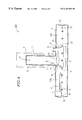
- FIG. 1 illustrates a cross-sectional view of a substrate processing device 100 of Example 1 according to the present invention.
- FIG. 2 is a cross-sectional view taken along line Z—Z in FIG. 1 .
- FIGS. 3A to 3 C are schematic figures illustrating the flow of a processing gas in the substrate processing device 100 .
- a plasma chamber 13 for generating plasma is provided in an upper portion of a vacuum chamber 1 so as to extend substantially perpendicularly to the longitudinal direction of the vacuum chamber 1 .
- the vacuum chamber 1 may be seen as consisting of two sections (i.e. , right-hand and left-hand sections) joined together where they meet the plasma chamber 13 .
- the plasma chamber 13 has an elongated plasma chamber opening 14 in a lower portion thereof.
- an RF electrode 8 and a dielectric window 16 via which an electric field from the RF electrode 8 is led into the plasma chamber 13 , are provided so as to be present on the right and left sides (as shown in FIG. 1 in this example)of the plasma chamber 13 .
- an excitation gas introduction nozzle 6 having a linear array of inlet holes for introducing an excitation gas is provided on the upper wall
- a reaction gas introduction nozzle 7 having a linear array of inlet holes for introducing a reaction gas is provided on the left side wall.
- an elongated vacuum discharge outlet 9 is provided adjacent the plasma chamber opening 14 so as to extend parallel to the plasma chamber 13 .
- the elongated vacuum discharge outlet 9 is located on the inner upper wall of the section of the vacuum chamber 1 away from the reaction gas introduction nozzle 7 (i.e., the right-hand section in FIG. 1 ).
- a first inert gas introduction nozzle 11 is provided which has inlet holes arranged so as to surround or encircle the plasma chamber opening 14 and the vacuum discharge outlet 9 .
- second inert gas introduction nozzles 12 On each (i.e., right or left) of the inner side walls of the vacuum chamber 1 , second inert gas introduction nozzles 12 having a linear array of inlet holes are provided.
- the first and second inert gas introduction nozzles 11 and 12 which are each composed of a porous pipe having an array of holes aligned with a predetermined pitch, are provided on the respective walls of the vacuum chamber 1 .
- the inlet holes of the second inert gas introduction nozzles 12 are arranged in one or more rows. Multiple rows of the second inert gas introduction nozzles 12 may be suitably provided depending upon the inner height of the vacuum chamber 1 .
- the first and second inert gas introduction nozzles 11 and 12 may be each defined by inlet holes which are formed directly on the walls of the chamber 1 , for example.
- a substrate holder 3 carrying a substrate 4 is placed on a conveyor mechanism 5 , and conveyed in the direction of arrow A (i.e., from left to right in FIG. 1) by the operation of the conveyor mechanism 5 .
- a heating section 2 is placed below the conveyor mechanism 5 .
- the longitudinal dimension of the heating section 2 is equal to or greater than the distance from the plasma chamber opening 14 to the vacuum discharge outlet 9 .
- the substrate holder 3 may include a resistor-based heating section.
- the conveyor mechanism 5 may have any structure, e.g., a roller or a rack-and-pinion mechanism.
- the excitation gas introduced from the excitation gas introduction nozzle 6 is excited by the RF electrode 8 through the dielectric window 16 . It is then mixed with the reaction gas introduced from the reaction gas introduction nozzle 7 .
- the mixed gases, herein referred to as a processing gas R, are led through the plasma chamber opening 14 so as to be discharged from a vacuum discharge outlet 9 .
- a first inert gas S 1 is introduced from a first inert gas introduction nozzle 11 .
- the processing gas R is substantially confined within the bounds of the first inert gas S 1 , which defines a processing zone 10 .
- linear flows of a second inert gas S 2 are introduced from the second inert gas introduction nozzles 12 so as to fill in right-hand and the left-hand spaces within the vacuum chamber 1 .
- the second inert gas S 2 is controlled so that the curtain-like flow of the first inert gas S 1 and the flow of processing gas R are not disturbed.
- FIGS. 3A through 3C sequentially show how the substrate 4 is conveyed.
- the substrate 4 carried on the substrate holder 3 is conveyed in the direction of arrow A by the conveyor mechanism 5 while being heated to a desired temperature by the heating section 2 , and passes through the processing zone 10 filled with processing gas R therein.
- the processing gas R undergoes a vapor-phase reaction, in the vicinity of the surface of the substrate 4 , which is heated to the desired temperature.
- the vapor-phase reaction provides a deposition, etching, or ashing effect on the surface of the substrate 4 , as determined by the specific types of gases employed.
- the first and second inert gases S 1 and S 2 may be Ar, He or N 2 , for example, as required by the type of process to which the substrate 4 is subjected.
- the first and second inert gases S 1 and S 2 may be the same or different inert gases.
- FIG. 4 shows a cross-sectional view of a substrate processing device 200 of Example 2 according to the present invention.
- the structure of the substrate processing device 200 of Example 2 of the present invention is substantially the same as that of the substrate processing device 100 of Example 1 except for the features described below.
- a processing zone separation wall 15 which spatially separates the processing zone 10 from the remaining zone 10 A, is disposed on the inner upper wall of the vacuum chamber 1 so as to surround or enclose the plasma chamber opening 14 and the vacuum discharge outlet 9 .
- the processing zone separation wall 15 prevents the flow of the processing gas R from being perturbed and mixed up by the first inert gas so as to be diffused in the vicinity of the inner upper wall of the vacuum chamber 1 .
- a first inert gas introduction nozzle 11 On the outside of the processing zone separation wall 15 is provided a first inert gas introduction nozzle 11 , having an array of inlet holes, the inlet holes being aligned along the processing zone separation wall 15 .
- a first inert gas S 1 introduced from the first inert gas introduction nozzle 11 forms a curtain-like gas flow along the processing zone separation wall 15 , so that the processing gas R is controlled so as not to flow out from the processing zone 10 .
- the first inert gas introduction nozzle 11 may be provided inside the processing zone separation wall 15 .
- the processing zone separation wall 15 and the curtain-like gas flow of the first inert gas S 1 along the processing zone separation wall 15 provide a synergetic effect to further prevent the processing gas R from escaping from the processing zone 10 , while maintaining a substantially constant flow of the processing gas R within the processing zone 10 .
- FIG. 5 shows a cross-sectional view of a substrate processing device 300 of Example 3 according to the present invention.
- the structure of the substrate processing device 300 is substantially the same as that of the substrate processing device 100 of Example 1 except for the features described below.
- aprocessing zone separation wall 15 which spatially separates the processing zone 10 from the remaining zone 10 A, is disposed on the inner upper wall of the vacuum chamber 1 so as to surround or enclose the plasma chamber opening 14 and the vacuum discharge outlet 9 .
- the processing zone separation wall 15 prevents the flow of the processing gas R from being perturbed and mixed up by the first inert gas so as to be diffused in the vicinity of the inner upper wall of the vacuum chamber 1 .
- a first inert gas introduction nozzle 11 having introduction holes located at a tip end of the processing zone separation wall 15 , is disposed on the processing zone separation wall 15 .
- a first inert gas S 1 introduced from the first inert gas introduction nozzle 11 forms a curtain-like gas flow emanating from the tip end of the processing zone separation wall 15 , so that the processing gas R is controlled so as not to flow out from the processing zone 10 .
- the processing zone separation wall 15 and the curtain-like gas flow of the first inert gas S 1 which emanates from the tip end of the processing zone separation wall 15 , and forms a curtain-like flow along the extention of the plane of the wall 15 , provide a synergetic effect.
- the escape of the processing gas R from the processing zone 10 can be further prevented while being able to maintain a substantially constant flow of the processing gas R in the processing zone 10 .
- the substrate processing device includes inert gas supplying sections (such as a first inert gas introduction section 11 and a second inert gas introduction section 12 ), so that the flow of aprocessing gas R is controlled by the flow of an inert gas S 1 , S 2 supplied from the inert gas supplying sections 11 , 12 thereby making it possible to subject the entire surface of a relatively large substrate 4 to uniform processing.
- inert gas supplying sections such as a first inert gas introduction section 11 and a second inert gas introduction section 12 .
- the introduced inert gas S 1 , S 2 forms a curtain-like flow surrounding the processing zone 10 .
- the processing conditions according to the present invention are highly reproducible.
- the separation wall 15 which surrounds the processing 10 zone so as to separate the processing zone from the other spaces 10 A
- the separation wall 15 and the inert gas S 11 , S 12 provide a synergetic effect.
- the processing conditions according to the present invention are highly reproducible.
- the separation wall 15 and the curtain-like flow of the inert gas create a synergetic effect.
- the processing conditions according to the present invention are highly reproducible.
Abstract
A substrate processing device of the present invention includes: a conveyor mechanism provided in a vacuum chamber for conveying a substrate thereon; a heating section provided within the vacuum chamber for heating the substrate; and a processing gas introduction section for introducing a processing gas to a processing zone within the vacuum chamber. A surface of the substrate is consecutively subjected to a predetermined process by: introducing a flow of the processing gas from the processing gas introduction section into the processing zone; conveying the substrate into and past the processing zone by means of the conveyor mechanism while heating the substrate by means of the heating section. The substrate processing device further includes an inert gas supplying section provided in the vacuum chamber for supplying an inert gas for controlling the flow of the processing gas.
Description
1. Field of the Invention
The present invention relates to a substrate processing device used for manufacturing a semiconductor device, a liquid crystal display device, a solar battery, and the like, more particularly to a substrate processing device such as a CVD (chemical vapor deposition) device, an etching device, an ashing device, and a sputtering device.
2. Description of the Related Art
As the substrate used for a liquid crystal display device becomes larger, the size of substrate processing devices such as a CVD device, an etching device, an ashing device, and a sputtering device increases correspondingly. Therefore, in the case of a plasma processing device of a parallel plate type, for example, it is becoming more and more difficult to perform a uniform process for the entire surface of a substrate.
As a method for solving this problem, a substrate processing device that consecutively processes a substrate while conveying it through an elongated linear-shaped processing zone has been suggested as disclosed in Japanese Laid-Open Publication No. 8-279498. The substrate processing device having such an elongated linear-shaped processing zone is shown in FIG. 6.
As shown in FIG. 6, in a substrate processing device 600 having an elongated linear-shaped processing zone 10, a substrate holder 3 carrying a substrate 4 is conveyed through a vacuum chamber 1 by a conveyor mechanism 5 while the substrate 4 is heated by a heating section 2.
On the other hand, an excitation gas introduced from an excitation gas introduction nozzle 6 is excited by an RF electrode 8 through a dielectric window 16. Also, a reaction gas is introduced by a reaction gas introduction nozzle 7. The excitation gas and the reaction gas pass through the processing zone 10 so as to be discharged from a vacuum discharge outlet 9 positioned parallel to the processing zone 10. When the substrate 4 passes through the processing zone 10 containing the excitation gas and the reaction gas as the surface of the substrate 4 is consecutively processed.
However, in the substrate processing device 600 described above, when the substrate 4 and the substrate holder 3 pass through the processing zone 10, spatial changes occur within the processing zone 10 due to the substrate 4 and the substrate holder 3 taking respectively different positions as shown in FIGS. 7A through 7C. Accordingly, the direction and rate of the flow of the processing gas near the surface of the substrate 4 may vary correspondingly. This results in a problem in that that the substrate 4 may be subjected to non-uniform processing, for example.
Moreover, because the processing gas diffuses to areas other than the processing zone 10, reaction components may adhere to be deposited as dust on the inner walls, observation window, and the like of the vacuum chamber 1.
FIGS. 7A , 7B, and 7C, sequentially, illustrate how the substrate 4 is conveyed.
According to one aspect of this invention, a substrate processing device includes: a conveyor mechanism provided in a vacuum chamber for conveying a substrate thereon; a heating section provided within the vacuum chamber for heating the substrate; and a processing gas introduction section for introducing a processing gas to a processing zone within the vacuum chamber. A surface of the substrate is consecutively subjected to a predetermined process by: introducing a flow of the processing gas from the processing gas introduction section into the processing zone; conveying the substrate into and past the processing zone by means of the conveyor mechanism while heating the substrate by means of the heating section. The substrate processing device further includes an inert gas supplying section provided in the vacuum chamber for supplying an inert gas for controlling the flow of the processing gas.
In one embodiment of the invention, the inert gas supplying section includes a first inert gas supplying section for supplying a first inert gas for controlling the flow of the processing gas so as not to substantially escape from the processing zone.
In another embodiment of the invention, the first inert gas supplying section substantially surrounds the processing zone.
In still another embodiment of the invention, the substrate processing device further includes a separation wall provided in the vacuum chamber for separating the processing zone from a remainder of the space in the vacuum chamber, the separation wall surrounding the processing zone.
In still yet another embodiment of the invention, the inert gas supplying section is provided along at least one of the inside and the outside of the separation wall.
In still another embodiment of the invention, the inert gas supplying section is provided at a tip end of the separation wall.
In still another embodiment of the invention, the inert gas supplying section further includes a second inert gas supplying section for supplying a second inert gas for controlling the flow of the processing gas and the first inert gas so as to prevent turbulence of the flows of the first inert gas and the processing gas.
In still another embodiment of the invention, the second inert gas supplying section is provided ahead of and behind the substrate being conveyed by the conveyor mechanism.
In still another embodiment of the invention, the processing gas introduction section includes: an excitation gas introduction section for introducing an excitation gas; and a reaction gas introduction section for introducing a reaction gas. The processing gas introduced into the processing zone comprises a mixture of the excitation gas and the reaction gas.
In still another embodiment of the invention, the inert gas includes at least one element selected from the group comprising Ar, He and N2.
A substrate processing device according to the present invention includes an inert gas supplying section, so that a flow of a processing gas is controlled by a flow of an inert gas supplied from inert gas supplying sections, thereby making it possible to prevent the processing gas from escaping from the processing zone while maintaining a substantially constant flow of the processing gas within the processing zone. Accordingly, it is possible to subject the entire surface of a substrate to uniform processing. In addition, it is possible to control dust deposition by preventing reaction components from adhering to inner walls of the vacuum chamber.
By disposing an inert gas supplying section so as to surround a processing zone, the introduced inert gas forms the curtain-like flow surrounding the processing zone. Accordingly, it is possible to prevent the processing gas from escaping from the processing zone while maintaining a substantially constant flow of the processing gas within the processing zone.
By providing a separation wall which surrounds the processing zone so as to separate the processing zone from the other spaces, the separation wall and the inert gas provide a synergetic effect. Accordingly, it is possible to prevent the processing gas from escaping from the processing zone while maintaining a substantially constant flow of the processing gas within the processing zone.
By providing an inert gas supplying section along the inside or outside of the separation wall, the separation wall and the curtain-like flow of the inert gas create a synergetic effect. Accordingly, it is possible to prevent the processing gas from escaping from the processing zone while maintaining a substantially constant flow of the processing gas within the processing zone.
By providing an inert gas supplying section at the tip end of the separation wall, it is possible to ensure that the curtain-like f low of the inert gas is formed along the extention of the plane of the separation wall. Accordingly, it is possible to prevent the processing gas from escaping from the processing zone while maintaining a substantially constant flow of the processing gas within the processing zone.
By providing inert gas supplying sections ahead of and behind the traveling substrate, it becomes possible to fill the spaces other than the processing zone with the inert gas, thereby preventing turbulence of the curtain-like flow of the inert gas and the flow of the processing gas.
Thus, the invention described herein makes possible the advantage of providing a substrate processing device which subjects a substrate to uniform processing by maintaining a flow of a processing gas in a predetermined direction and at a constant rate near the surface of the substrate, irrespective of any spatial changes occurring in the processing zone with the positioning of the substrate, and suppresses the deposition of dust particles by concentrating the processing gas into the processing zone.
This advantage of the present invention will become apparent to those skilled in the art upon reading and understanding the following detailed description with reference to the accompanying figures.
FIG. 1 shows a cross-sectional view of a substrate processing device according to Example 1 of the present invention.
FIG. 2 shows a cross-sectional view taken along line Z—Z in FIG. 1.
FIGS. 3A to 3C are schematic figures illustrating the flow of a processing gas in a substrate processing device according to Example 1 of the present invention.
FIG. 4 is a cross-sectional view of a substrate processing device according to Example 2 of the present invention.
FIG. 5 is a cross-sectional view of a substrate processing device according to Example 3 of the present invention.
FIG. 6 is a cross-sectional view of a conventional substrate processing device.
FIGS. 7A to 7C are schematic figures illustrating the flow of a processing gas in the conventional substrate processing device.
Hereinafter, the present invention will be described by way of examples with reference to FIGS. 1 through 5.
FIG. 1 illustrates a cross-sectional view of a substrate processing device 100 of Example 1 according to the present invention. FIG. 2 is a cross-sectional view taken along line Z—Z in FIG. 1. FIGS. 3A to 3C are schematic figures illustrating the flow of a processing gas in the substrate processing device 100.
As shown in FIGS. 1 and 2, in accordance with a substrate processing device 100 of the present example, a plasma chamber 13 for generating plasma is provided in an upper portion of a vacuum chamber 1 so as to extend substantially perpendicularly to the longitudinal direction of the vacuum chamber 1. Thus, the vacuum chamber 1 may be seen as consisting of two sections (i.e. , right-hand and left-hand sections) joined together where they meet the plasma chamber 13. The plasma chamber 13 has an elongated plasma chamber opening 14 in a lower portion thereof.
On the outside of the plasma chamber 13, an RF electrode 8 and a dielectric window 16, via which an electric field from the RF electrode 8 is led into the plasma chamber 13, are provided so as to be present on the right and left sides (as shown in FIG. 1 in this example)of the plasma chamber 13. On the inside of the plasma chamber 13, an excitation gas introduction nozzle 6 having a linear array of inlet holes for introducing an excitation gas is provided on the upper wall, and a reaction gas introduction nozzle 7 having a linear array of inlet holes for introducing a reaction gas is provided on the left side wall.
On the inner upper wall of the vacuum chamber 1, an elongated vacuum discharge outlet 9 is provided adjacent the plasma chamber opening 14 so as to extend parallel to the plasma chamber 13. Specifically, the elongated vacuum discharge outlet 9 is located on the inner upper wall of the section of the vacuum chamber 1 away from the reaction gas introduction nozzle 7 (i.e., the right-hand section in FIG. 1). In addition, on the inner upper wall of the vacuum chamber 1, a first inert gas introduction nozzle 11 is provided which has inlet holes arranged so as to surround or encircle the plasma chamber opening 14 and the vacuum discharge outlet 9. On each (i.e., right or left) of the inner side walls of the vacuum chamber 1, second inert gas introduction nozzles 12 having a linear array of inlet holes are provided. Thus, the first and second inert gas introduction nozzles 11 and 12 which are each composed of a porous pipe having an array of holes aligned with a predetermined pitch, are provided on the respective walls of the vacuum chamber 1. The inlet holes of the second inert gas introduction nozzles 12 are arranged in one or more rows. Multiple rows of the second inert gas introduction nozzles 12 may be suitably provided depending upon the inner height of the vacuum chamber 1. Alternatively, the first and second inert gas introduction nozzles 11 and 12, respectively, may be each defined by inlet holes which are formed directly on the walls of the chamber 1, for example.
Moreover, in the vacuum chamber 1, a substrate holder 3 carrying a substrate 4 is placed on a conveyor mechanism 5, and conveyed in the direction of arrow A (i.e., from left to right in FIG. 1) by the operation of the conveyor mechanism 5. Moreover, a heating section 2 is placed below the conveyor mechanism 5. The longitudinal dimension of the heating section 2 is equal to or greater than the distance from the plasma chamber opening 14 to the vacuum discharge outlet 9. In the alternative or in addition, the substrate holder 3 may include a resistor-based heating section. The conveyor mechanism 5 may have any structure, e.g., a roller or a rack-and-pinion mechanism.
Next, a gas flow will be described with reference to FIGS. 3A through 3C. The excitation gas introduced from the excitation gas introduction nozzle 6 is excited by the RF electrode 8 through the dielectric window 16. It is then mixed with the reaction gas introduced from the reaction gas introduction nozzle 7. The mixed gases, herein referred to as a processing gas R, are led through the plasma chamber opening 14 so as to be discharged from a vacuum discharge outlet 9.
On the other hand, a first inert gas S1 is introduced from a first inert gas introduction nozzle 11. By a curtain-like flow of the first inert gas S1, the processing gas R is substantially confined within the bounds of the first inert gas S1, which defines a processing zone 10.
In addition, linear flows of a second inert gas S2 are introduced from the second inert gas introduction nozzles 12 so as to fill in right-hand and the left-hand spaces within the vacuum chamber 1. The second inert gas S2 is controlled so that the curtain-like flow of the first inert gas S1 and the flow of processing gas R are not disturbed.
FIGS. 3A through 3C sequentially show how the substrate 4 is conveyed.
As shown, the substrate 4 carried on the substrate holder 3 is conveyed in the direction of arrow A by the conveyor mechanism 5 while being heated to a desired temperature by the heating section 2, and passes through the processing zone 10 filled with processing gas R therein. The processing gas R undergoes a vapor-phase reaction, in the vicinity of the surface of the substrate 4, which is heated to the desired temperature. As a result, the surface of the substrate 4 is consecutively processed. The vapor-phase reaction provides a deposition, etching, or ashing effect on the surface of the substrate 4, as determined by the specific types of gases employed.
The first and second inert gases S1 and S2, may be Ar, He or N2, for example, as required by the type of process to which the substrate 4 is subjected. The first and second inert gases S1 and S2 may be the same or different inert gases.
FIG. 4 shows a cross-sectional view of a substrate processing device 200 of Example 2 according to the present invention. The structure of the substrate processing device 200 of Example 2 of the present invention is substantially the same as that of the substrate processing device 100 of Example 1 except for the features described below.
As shown in FIG. 4, in accordance with the substrate processing device 200 of the present example, a processing zone separation wall 15, which spatially separates the processing zone 10 from the remaining zone 10A, is disposed on the inner upper wall of the vacuum chamber 1 so as to surround or enclose the plasma chamber opening 14 and the vacuum discharge outlet 9. The processing zone separation wall 15 prevents the flow of the processing gas R from being perturbed and mixed up by the first inert gas so as to be diffused in the vicinity of the inner upper wall of the vacuum chamber 1.
On the outside of the processing zone separation wall 15 is provided a first inert gas introduction nozzle 11, having an array of inlet holes, the inlet holes being aligned along the processing zone separation wall 15. A first inert gas S1 introduced from the first inert gas introduction nozzle 11 forms a curtain-like gas flow along the processing zone separation wall 15, so that the processing gas R is controlled so as not to flow out from the processing zone 10.
Alternatively, the first inert gas introduction nozzle 11 may be provided inside the processing zone separation wall 15.
As described above, the processing zone separation wall 15 and the curtain-like gas flow of the first inert gas S1 along the processing zone separation wall 15 provide a synergetic effect to further prevent the processing gas R from escaping from the processing zone 10, while maintaining a substantially constant flow of the processing gas R within the processing zone 10.
FIG. 5 shows a cross-sectional view of a substrate processing device 300 of Example 3 according to the present invention. The structure of the substrate processing device 300 is substantially the same as that of the substrate processing device 100 of Example 1 except for the features described below.
As shown in FIG. 5, in accordance with the substrate processing device 300 of Example 3, aprocessing zone separation wall 15, which spatially separates the processing zone 10 from the remaining zone 10A, is disposed on the inner upper wall of the vacuum chamber 1 so as to surround or enclose the plasma chamber opening 14 and the vacuum discharge outlet 9. The processing zone separation wall 15 prevents the flow of the processing gas R from being perturbed and mixed up by the first inert gas so as to be diffused in the vicinity of the inner upper wall of the vacuum chamber 1.
A first inert gas introduction nozzle 11, having introduction holes located at a tip end of the processing zone separation wall 15, is disposed on the processing zone separation wall 15. A first inert gas S1 introduced from the first inert gas introduction nozzle 11 forms a curtain-like gas flow emanating from the tip end of the processing zone separation wall 15, so that the processing gas R is controlled so as not to flow out from the processing zone 10.
As described above, the processing zone separation wall 15 and the curtain-like gas flow of the first inert gas S1, which emanates from the tip end of the processing zone separation wall 15, and forms a curtain-like flow along the extention of the plane of the wall 15, provide a synergetic effect. As a result, the escape of the processing gas R from the processing zone 10 can be further prevented while being able to maintain a substantially constant flow of the processing gas R in the processing zone 10.
As described above, the substrate processing device according to the present invention includes inert gas supplying sections (such as a first inert gas introduction section 11 and a second inert gas introduction section 12), so that the flow of aprocessing gas R is controlled by the flow of an inert gas S1, S2 supplied from the inert gas supplying sections 11, 12 thereby making it possible to subject the entire surface of a relatively large substrate 4 to uniform processing. In addition, it is possible to control dust deposition by preventing reaction components from adhering to inner walls of the vacuum chamber 1. Moreover, the processing conditions according to the present invention are highly reproducible.
By disposing an inert gas supplying section 11, 12 so as to surround a processing zone 10, the introduced inert gas S1, S2 forms a curtain-like flow surrounding the processing zone 10. As a result, it becomes possible to subject the entire surface of a relatively large substrate 4 to uniform processing. In addition, it is possible to control dust deposition by preventing reaction components from adhering to inner walls of the vacuum chamber 1. Moreover, the processing conditions according to the present invention are highly reproducible.
By providing a separation wall 15 which surrounds the processing 10 zone so as to separate the processing zone from the other spaces 10A, the separation wall 15 and the inert gas S11, S12 provide a synergetic effect. As a result, it becomes possible to subject the entire surface of a relatively large substrate 4 to uniform processing. In addition, it is possible to control dust deposition by preventing reaction components from adhering to inner walls of the vacuum chamber 1. Moreover, the processing conditions according to the present invention are highly reproducible.
By providing an inert gas supplying section along the inside or outside of the separation wall 15, the separation wall 15 and the curtain-like flow of the inert gas create a synergetic effect. As a result, it becomes possible to subject the entire surface of a relatively large substrate 4 to uniform processing. In addition, it is possible to control dust deposition by preventing reaction components from adhering to inner walls of the vacuum chamber 1. Moreover, the processing conditions according to the present invention are highly reproducible.
By providing an inert gas supplying section 11 at the tip end of the separation wall 15, it is possible to ensure that the curtain-like flow of the inert gas S1 forms a curtain-like flow along the extension of the plane of the separation wall 15. As a result, it becomes possible to subject the entire surface of a relatively large substrate 4 to uniform processing. In addition, it is possible to control dust deposition by preventing reaction components from adhering to inner walls of the vacuum chamber 1. Moreover, the processing conditions according to the present invention are highly reproducible.
By providing an inert gas supplying sections 12 ahead of and behind the traveling substrate 4, it becomes possible to fill the spaces other than the processing zone 10A with the inert gas S2, thereby preventing turbulence of the curtain-like flow of the inert gas S1 and the flow of the processing gas R. As a result, it becomes possible to subject the entire surf ace of a relatively large substrate 4 to uniform processing. In addition, it is possible to control dust deposition by preventing reaction components from adhering to inner walls of the vacuum chamber 1. Moreover, the processing conditions according to the present invention are highly reproducible.
Various other modifications will be apparent to and can be readily made by those skilled in the art without departing from the scope and spirit of this invention. Accordingly, it is not intended that the scope of the claims appended hereto be limited to the description as set forth herein, but rather that the claims be broadly construed.
Claims (8)
1. A substrate processing device, comprising:
a conveyor mechanism provided in a vacuum chamber for conveying a substrate thereon;
a heating section provided within the vacuum chamber for heating the substrate; and
a processing gas introduction section for introducing a processing gas to a processing zone within the vacuum chamber; wherein
a surface of the substrate is consecutively subjected to a predetermined process by: introducing a flow of the processing gas from the processing gas introduction section into the processing zone; and conveying the substrate into and past the processing section by means of the conveyor mechanism while heating the substrate by means of the heating section, and wherein the substrate processing device further comprises:
an inert gas supplying section provided in the vacuum chamber for supplying an inert gas for controlling the flow of the process gas, wherein the inert gas supplying section comprises a first inert supplying section, which substantially surrounds the processing zone and is approximately perpendicular to the substrate being conveyed by the conveyor mechanism, and a second inert gas supplying section, which is provided ahead of and behind, and is approximately parallel to the substrate being conveyed by the conveyor mechanism.
2. A substrate processing device according to claim 1, wherein the first inert gas supplying section supplies a first inert gas for controlling the flow of the processing gas so as not to substantially escape from the processing zone.
3. A substrate processing device according to claim 2, wherein the second inert gas supplying section supplies a second inert gas for controlling the flow of the processing gas and the first inert gas so as to prevent turbulence of the flows of the first inert gas and the processing gas.
4. A substrate processing device according to claim 1, further comprising a separation wall provided in the vacuum chamber for separating the processing zone from a remainder of the space in the vacuum chamber, the separation wall surrounding the processing zone.
5. A substrate processing device according to claim 4, wherein the inert gas supplying section is provided along at least one of the inside and the outside of the separation wall.
6. A substrate processing device according to claim 4, wherein the inert gas supplying section is provided at a tip end of the separation wall.
7. A substrate processing device according to claim 1, wherein the processing gas introduction section comprises:
an excitation gas introduction section for introducing an excitation gas; and
a reaction gas introduction section for introducing a reaction gas, and wherein
the processing gas introduced into the processing zone comprises a mixture of the excitation gas and the reaction gas.
8. A substrate processing device according to claim 1, wherein the inert gas includes at least one element selected from the group comprising Ar, He and N2.
Applications Claiming Priority (2)
| Application Number | Priority Date | Filing Date | Title |
|---|---|---|---|
| JP14241198A JP3349953B2 (en) | 1998-05-25 | 1998-05-25 | Substrate processing equipment |
| JP10-142411 | 1998-05-25 |
Publications (1)
| Publication Number | Publication Date |
|---|---|
| US6187101B1 true US6187101B1 (en) | 2001-02-13 |
Family
ID=15314721
Family Applications (1)
| Application Number | Title | Priority Date | Filing Date |
|---|---|---|---|
| US09/318,090 Expired - Lifetime US6187101B1 (en) | 1998-05-25 | 1999-05-25 | Substrate processing device |
Country Status (2)
| Country | Link |
|---|---|
| US (1) | US6187101B1 (en) |
| JP (1) | JP3349953B2 (en) |
Cited By (17)
| Publication number | Priority date | Publication date | Assignee | Title |
|---|---|---|---|---|
| US20030215569A1 (en) * | 2002-05-17 | 2003-11-20 | Mardian Allen P. | Chemical vapor deposition apparatus and deposition method |
| US20040083959A1 (en) * | 2001-03-13 | 2004-05-06 | Carpenter Craig M. | Chemical vapor deposition apparatuses and deposition methods |
| US20050028732A1 (en) * | 2002-01-22 | 2005-02-10 | Mardian Allen P. | Chemical vapor deposition method |
| US20050039687A1 (en) * | 2001-10-26 | 2005-02-24 | Seagate Technology Llc | In-line, pass-by system and method for disc vapor lubrication |
| US20070049057A1 (en) * | 2005-08-25 | 2007-03-01 | Tae-Hoon Yang | Heat treatment apparatus and heat treatment method using the same |
| US20070203508A1 (en) * | 2006-02-28 | 2007-08-30 | Arthrocare Corporation | Bone anchor suture-loading system, method and apparatus |
| US7393562B2 (en) | 2002-02-25 | 2008-07-01 | Micron Technology, Inc. | Deposition methods for improved delivery of metastable species |
| US7399499B2 (en) | 2002-08-15 | 2008-07-15 | Micron Technology, Inc. | Methods of gas delivery for deposition processes and methods of depositing material on a substrate |
| US20090165716A1 (en) * | 2008-01-01 | 2009-07-02 | Dongguan Anwell Digital Machinery Ltd. | Method and system for plasma enhanced chemical vapor deposition |
| EP2202785A1 (en) * | 2007-09-04 | 2010-06-30 | Sharp Kabushiki Kaisha | Plasma treatment apparatus, plasma treatment method, and semiconductor element |
| US20120266818A1 (en) * | 2011-04-21 | 2012-10-25 | Creating Nano Technologies, Inc. | Atmospheric film-coating device and film-manufacturing apparatus |
| US20130337193A1 (en) * | 2010-10-22 | 2013-12-19 | Agc Glass Europe | Modular coater separation |
| US20140151333A1 (en) * | 2009-12-03 | 2014-06-05 | Lam Research Corporation | Small Plasma Chamber Systems and Methods |
| CN113832448A (en) * | 2020-06-23 | 2021-12-24 | 拓荆科技股份有限公司 | Semiconductor film deposition equipment and semiconductor film coating method |
| CN113862624A (en) * | 2021-09-27 | 2021-12-31 | 上海集成电路材料研究院有限公司 | Sputtering deposition equipment and sputtering deposition method |
| US20220230854A1 (en) * | 2015-10-28 | 2022-07-21 | Vito Nv | Apparatus for indirect atmospheric pressure plasma processing |
| US11513378B2 (en) * | 2018-09-30 | 2022-11-29 | HKC Corporation | Display panel manufacturing device and cleaning method |
Families Citing this family (2)
| Publication number | Priority date | Publication date | Assignee | Title |
|---|---|---|---|---|
| JP4991950B1 (en) * | 2011-04-13 | 2012-08-08 | シャープ株式会社 | Mist deposition system |
| JP5860668B2 (en) * | 2011-10-28 | 2016-02-16 | 東京エレクトロン株式会社 | Manufacturing method of semiconductor device |
Citations (9)
| Publication number | Priority date | Publication date | Assignee | Title |
|---|---|---|---|---|
| US4430749A (en) * | 1981-06-30 | 1984-02-07 | Siemens Gammasonics, Inc. | Medical imaging apparatus and method for furnishing difference images |
| US5090356A (en) * | 1991-06-28 | 1992-02-25 | United Solar Systems Corporation | Chemically active isolation passageway for deposition chambers |
| US5372646A (en) * | 1992-05-12 | 1994-12-13 | Solar Cells, Inc. | Apparatus for making photovoltaic devices |
| US5413671A (en) * | 1993-08-09 | 1995-05-09 | Advanced Micro Devices, Inc. | Apparatus and method for removing deposits from an APCVD system |
| JPH08279498A (en) | 1995-02-03 | 1996-10-22 | Sharp Corp | Equipment and method for line plasma vapor phase accumulation |
| US5688359A (en) * | 1995-07-20 | 1997-11-18 | Micron Technology, Inc. | Muffle etch injector assembly |
| US5863338A (en) * | 1992-11-27 | 1999-01-26 | Matsushita Electric Industrial Co., Ltd. | Apparatus and method for forming thin film |
| US5976258A (en) * | 1998-02-05 | 1999-11-02 | Semiconductor Equipment Group, Llc | High temperature substrate transfer module |
| US6056824A (en) * | 1998-01-16 | 2000-05-02 | Silicon Valley Group Thermal Systems | Free floating shield and semiconductor processing system |
-
1998
- 1998-05-25 JP JP14241198A patent/JP3349953B2/en not_active Expired - Fee Related
-
1999
- 1999-05-25 US US09/318,090 patent/US6187101B1/en not_active Expired - Lifetime
Patent Citations (9)
| Publication number | Priority date | Publication date | Assignee | Title |
|---|---|---|---|---|
| US4430749A (en) * | 1981-06-30 | 1984-02-07 | Siemens Gammasonics, Inc. | Medical imaging apparatus and method for furnishing difference images |
| US5090356A (en) * | 1991-06-28 | 1992-02-25 | United Solar Systems Corporation | Chemically active isolation passageway for deposition chambers |
| US5372646A (en) * | 1992-05-12 | 1994-12-13 | Solar Cells, Inc. | Apparatus for making photovoltaic devices |
| US5863338A (en) * | 1992-11-27 | 1999-01-26 | Matsushita Electric Industrial Co., Ltd. | Apparatus and method for forming thin film |
| US5413671A (en) * | 1993-08-09 | 1995-05-09 | Advanced Micro Devices, Inc. | Apparatus and method for removing deposits from an APCVD system |
| JPH08279498A (en) | 1995-02-03 | 1996-10-22 | Sharp Corp | Equipment and method for line plasma vapor phase accumulation |
| US5688359A (en) * | 1995-07-20 | 1997-11-18 | Micron Technology, Inc. | Muffle etch injector assembly |
| US6056824A (en) * | 1998-01-16 | 2000-05-02 | Silicon Valley Group Thermal Systems | Free floating shield and semiconductor processing system |
| US5976258A (en) * | 1998-02-05 | 1999-11-02 | Semiconductor Equipment Group, Llc | High temperature substrate transfer module |
Cited By (30)
| Publication number | Priority date | Publication date | Assignee | Title |
|---|---|---|---|---|
| US20040083959A1 (en) * | 2001-03-13 | 2004-05-06 | Carpenter Craig M. | Chemical vapor deposition apparatuses and deposition methods |
| US20040216671A1 (en) * | 2001-03-13 | 2004-11-04 | Carpenter Craig M | Chemical vapor deposition apparatuses |
| US7378127B2 (en) | 2001-03-13 | 2008-05-27 | Micron Technology, Inc. | Chemical vapor deposition methods |
| US7828899B2 (en) * | 2001-10-26 | 2010-11-09 | Seagate Technology Llc | In-line, pass-by system and method for disc vapor lubrication |
| US20050039687A1 (en) * | 2001-10-26 | 2005-02-24 | Seagate Technology Llc | In-line, pass-by system and method for disc vapor lubrication |
| US7229666B2 (en) * | 2002-01-22 | 2007-06-12 | Micron Technology, Inc. | Chemical vapor deposition method |
| US20050028732A1 (en) * | 2002-01-22 | 2005-02-10 | Mardian Allen P. | Chemical vapor deposition method |
| US7393562B2 (en) | 2002-02-25 | 2008-07-01 | Micron Technology, Inc. | Deposition methods for improved delivery of metastable species |
| US7527693B2 (en) | 2002-02-25 | 2009-05-05 | Micron Technology, Inc. | Apparatus for improved delivery of metastable species |
| US7468104B2 (en) | 2002-05-17 | 2008-12-23 | Micron Technology, Inc. | Chemical vapor deposition apparatus and deposition method |
| US20030215569A1 (en) * | 2002-05-17 | 2003-11-20 | Mardian Allen P. | Chemical vapor deposition apparatus and deposition method |
| US7399499B2 (en) | 2002-08-15 | 2008-07-15 | Micron Technology, Inc. | Methods of gas delivery for deposition processes and methods of depositing material on a substrate |
| US20070049057A1 (en) * | 2005-08-25 | 2007-03-01 | Tae-Hoon Yang | Heat treatment apparatus and heat treatment method using the same |
| US7862334B2 (en) * | 2005-08-25 | 2011-01-04 | Samsung Mobile Display Co., Ltd. | Heat treatment apparatus and heat treatment method using the same |
| US20070203508A1 (en) * | 2006-02-28 | 2007-08-30 | Arthrocare Corporation | Bone anchor suture-loading system, method and apparatus |
| EP2202785A1 (en) * | 2007-09-04 | 2010-06-30 | Sharp Kabushiki Kaisha | Plasma treatment apparatus, plasma treatment method, and semiconductor element |
| EP2202785A4 (en) * | 2007-09-04 | 2010-11-10 | Sharp Kk | Plasma treatment apparatus, plasma treatment method, and semiconductor element |
| US20100193915A1 (en) * | 2007-09-04 | 2010-08-05 | Katsushi Kishimoto | Plasma processing apparatus and plasma processing method, and semiconductor device |
| US8395250B2 (en) | 2007-09-04 | 2013-03-12 | Kabushiki Kaisha Sharp | Plasma processing apparatus with an exhaust port above the substrate |
| US20090165716A1 (en) * | 2008-01-01 | 2009-07-02 | Dongguan Anwell Digital Machinery Ltd. | Method and system for plasma enhanced chemical vapor deposition |
| US20140151333A1 (en) * | 2009-12-03 | 2014-06-05 | Lam Research Corporation | Small Plasma Chamber Systems and Methods |
| US9911578B2 (en) * | 2009-12-03 | 2018-03-06 | Lam Research Corporation | Small plasma chamber systems and methods |
| US9938617B2 (en) * | 2010-10-22 | 2018-04-10 | Agc Glass Europe | Modular coater separation |
| US20130337193A1 (en) * | 2010-10-22 | 2013-12-19 | Agc Glass Europe | Modular coater separation |
| US20120266818A1 (en) * | 2011-04-21 | 2012-10-25 | Creating Nano Technologies, Inc. | Atmospheric film-coating device and film-manufacturing apparatus |
| US20220230854A1 (en) * | 2015-10-28 | 2022-07-21 | Vito Nv | Apparatus for indirect atmospheric pressure plasma processing |
| US11513378B2 (en) * | 2018-09-30 | 2022-11-29 | HKC Corporation | Display panel manufacturing device and cleaning method |
| CN113832448A (en) * | 2020-06-23 | 2021-12-24 | 拓荆科技股份有限公司 | Semiconductor film deposition equipment and semiconductor film coating method |
| CN113832448B (en) * | 2020-06-23 | 2023-06-09 | 拓荆科技股份有限公司 | Semiconductor film deposition equipment and semiconductor film coating method |
| CN113862624A (en) * | 2021-09-27 | 2021-12-31 | 上海集成电路材料研究院有限公司 | Sputtering deposition equipment and sputtering deposition method |
Also Published As
| Publication number | Publication date |
|---|---|
| JPH11340145A (en) | 1999-12-10 |
| JP3349953B2 (en) | 2002-11-25 |
Similar Documents
| Publication | Publication Date | Title |
|---|---|---|
| US6187101B1 (en) | Substrate processing device | |
| KR100552378B1 (en) | Electrode Structure of The Plasma Surface Treatment Device | |
| US6022414A (en) | Single body injector and method for delivering gases to a surface | |
| KR100817464B1 (en) | Directing a flow of gas in a substrate processing chamber | |
| EP0697376B1 (en) | Single body injector and method for delivering gases to a surface | |
| US6303501B1 (en) | Gas mixing apparatus and method | |
| KR100539890B1 (en) | Substrate processing apparatus | |
| US20040118519A1 (en) | Blocker plate bypass design to improve clean rate at the edge of the chamber | |
| US6068703A (en) | Gas mixing apparatus and method | |
| EP1638139A1 (en) | Plasma processing device | |
| US20090277386A1 (en) | Catalytic chemical vapor deposition apparatus | |
| EP0254654A1 (en) | Method of chemical vapor deposition | |
| JP2002503030A (en) | High Selectivity Etching Using External Plasma Discharge | |
| US7217326B2 (en) | Chemical vapor deposition apparatus | |
| CN109314055A (en) | Atomic layer growth device and atomic layer growth method | |
| JPH10330944A (en) | Substrate treating device | |
| JP2005033167A (en) | Shower plate, plasma processing device and method of producing products | |
| WO2005067022A1 (en) | Shower plate, plasma processing system, and process for producing product | |
| US6673156B2 (en) | Semiconductor processing device | |
| KR20210145314A (en) | Electrostatic chuck with spatially tunable RF coupling to wafer | |
| KR100373434B1 (en) | Dielectric film formation method with reduced metal contaminants | |
| JP7398630B2 (en) | plasma processing equipment | |
| JPH0618177B2 (en) | Semiconductor device manufacturing equipment | |
| KR101935881B1 (en) | Treatment apparatus for large area substrate, Gas supplying apparatus for large area substrate and Showerhead support unit | |
| JP2001023910A (en) | Semiconductor manufacturing apparatus |
Legal Events
| Date | Code | Title | Description |
|---|---|---|---|
| AS | Assignment |
Owner name: SHARP KABUSHIKI KAISHA, JAPAN Free format text: ASSIGNMENT OF ASSIGNORS INTEREST;ASSIGNOR:YOSHIZAWA, TAKASHI;REEL/FRAME:010003/0635 Effective date: 19990420 |
|
| FEPP | Fee payment procedure |
Free format text: PAYOR NUMBER ASSIGNED (ORIGINAL EVENT CODE: ASPN); ENTITY STATUS OF PATENT OWNER: LARGE ENTITY |
|
| STCF | Information on status: patent grant |
Free format text: PATENTED CASE |
|
| FPAY | Fee payment |
Year of fee payment: 4 |
|
| FPAY | Fee payment |
Year of fee payment: 8 |
|
| FPAY | Fee payment |
Year of fee payment: 12 |