US6190236B1 - Method and system for vacuum removal of chemical mechanical polishing by-products - Google Patents
Method and system for vacuum removal of chemical mechanical polishing by-products Download PDFInfo
- Publication number
- US6190236B1 US6190236B1 US08/732,165 US73216596A US6190236B1 US 6190236 B1 US6190236 B1 US 6190236B1 US 73216596 A US73216596 A US 73216596A US 6190236 B1 US6190236 B1 US 6190236B1
- Authority
- US
- United States
- Prior art keywords
- vacuum
- polishing
- nozzle
- polishing pad
- product particles
- Prior art date
- Legal status (The legal status is an assumption and is not a legal conclusion. Google has not performed a legal analysis and makes no representation as to the accuracy of the status listed.)
- Expired - Lifetime
Links
Images


Classifications
-
- B—PERFORMING OPERATIONS; TRANSPORTING
- B24—GRINDING; POLISHING
- B24B—MACHINES, DEVICES, OR PROCESSES FOR GRINDING OR POLISHING; DRESSING OR CONDITIONING OF ABRADING SURFACES; FEEDING OF GRINDING, POLISHING, OR LAPPING AGENTS
- B24B37/00—Lapping machines or devices; Accessories
- B24B37/11—Lapping tools
- B24B37/20—Lapping pads for working plane surfaces
- B24B37/26—Lapping pads for working plane surfaces characterised by the shape of the lapping pad surface, e.g. grooved
-
- B—PERFORMING OPERATIONS; TRANSPORTING
- B24—GRINDING; POLISHING
- B24B—MACHINES, DEVICES, OR PROCESSES FOR GRINDING OR POLISHING; DRESSING OR CONDITIONING OF ABRADING SURFACES; FEEDING OF GRINDING, POLISHING, OR LAPPING AGENTS
- B24B53/00—Devices or means for dressing or conditioning abrasive surfaces
- B24B53/017—Devices or means for dressing, cleaning or otherwise conditioning lapping tools
-
- B—PERFORMING OPERATIONS; TRANSPORTING
- B24—GRINDING; POLISHING
- B24B—MACHINES, DEVICES, OR PROCESSES FOR GRINDING OR POLISHING; DRESSING OR CONDITIONING OF ABRADING SURFACES; FEEDING OF GRINDING, POLISHING, OR LAPPING AGENTS
- B24B55/00—Safety devices for grinding or polishing machines; Accessories fitted to grinding or polishing machines for keeping tools or parts of the machine in good working condition
- B24B55/12—Devices for exhausting mist of oil or coolant; Devices for collecting or recovering materials resulting from grinding or polishing, e.g. of precious metals, precious stones, diamonds or the like
Definitions
- the field of the present invention pertains to semiconductor fabrication processing. More particularly, the present invention relates to a system for removing polishing by-products of a semiconductor wafer and polishing pad from a chemical mechanical polishing machine.
- the geometry of the features of the IC components are commonly defined photographically through a process known as photolithography. Very fine surface geometries can be reproduced accurately by this technique.
- the photolithography process is used to define component regions and build up components one layer on top of another. Complex ICs can often have many different built up layers, each layer having components, each layer having differing interconnections, and each layer stacked on top of the previous layer. The resulting topography of these complex IC's often resemble familiar terrestrial “mountain ranges”, with many “hills” and “valleys” as the IC components are built up on the underlying surface of the silicon wafer.
- a mask image, or pattern, defining the various components is focused onto a photosensitive layer using ultraviolet light.
- the image is focused onto the surface using the optical means of the photolithography tool, and is imprinted into the photosensitive layer.
- optical resolution must increase.
- the depth of focus of the mask image correspondingly narrows. This is due to the narrow range in depth of focus imposed by the high numerical aperture lenses in the photolithography tool. This narrowing depth of focus is often the limiting factor in the degree of resolution obtainable, and thus, the smallest components obtainable using the photolithography tool.
- a precisely flat surface is desired.
- the precisely flat (i.e. fully planarized) surface will allow for extremely small depths of focus, and in turn, allow the definition and subsequent fabrication of extremely small components.
- CMP Chemical-mechanical polishing
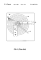
- FIG. 1 shows a down view of a CMP machine 100 and FIG. 2 shows a side view of the CMP machine 100 .
- the CMP machine 100 is fed wafers to be polished.
- the CMP machine 100 picks up the wafers with an arm 101 and places them onto a rotating polishing pad 102 .
- the polishing pad 102 is made of a resilient material and is textured, often with a plurality of predetermined groves 103 , to aid the polishing process.
- the polishing pad 102 rotates on a platen 104 , or turn table located beneath the polishing pad 102 , at a predetermined speed.
- a wafer 105 is held in place on the polishing pad 102 and the arm 101 by a carrier ring 112 and a carrier film 106 .
- the lower surface of the wafer 105 rests against the polishing pad 102 .
- the upper surface of the wafer 105 is against the lower surface of the carrier film 106 of the arm 101 .
- the arm 101 rotates the wafer 105 at a predetermined rate.
- the arm 101 forces the wafer 105 into the polishing pad 102 with a predetermined amount of down force.
- the CMP machine 100 also includes a slurry dispense arm 107 extending across the radius of the polishing pad 102 .
- the slurry dispense arm 107 dispenses a flow of slurry onto the polishing pad 102 .
- the slurry is a mixture of de ionized water and polishing agents designed to chemically aid the smooth and predictable planerization of the wafer.
- the rotating action of both the polishing pad 102 and the wafer 105 in conjunction with the polishing action of the slurry, combine to planerize, or polish, the wafer 105 at some nominal rate. This rate is referred to as the removal rate.
- a constant and predictable removal rate is important to the uniformity and through put performance of the wafer fabrication process.
- the removal rate should be expedient, yet yield precisely planerized wafers, free from surface anomalies. If the removal rate is too slow, the number of planarized wafers produced in a given period of time decreases, hurting wafer through-put of the fabrication process. If the removal rate is too fast, the CMP planarization process will not be uniform across the surface of the wafers, hurting the yield of the fabrication process.
- the CMP machine 100 includes a conditioner assembly 120 .
- the conditioner assembly 120 includes a conditioner arm 108 , which extends across the radius of the polishing pad 102 .
- An end effector 109 is connected to the conditioner arm 108 .
- the end effector 109 includes an abrasive conditioning disk 110 which is used to roughen the surface of the polishing pad 102 .
- the conditioning disk 110 is rotated by the conditioner arm 108 and is translationally moved towards the center of the polishing pad and away from the center of the polishing pad 102 , such that the conditioning disk 110 covers the radius of the polishing pad 102 . In so doing, conditioning disk 110 covers the surface area of the polishing pad 102 , as polishing pad 102 rotates.
- a polishing pad having a roughened surface has an increased number of very small pits and gouges in its surface from the conditioner assembly 120 and therefore produces a faster removal rate via increased slurry transfer to the surface of the wafer. Without conditioning, the surface of polishing pad 102 is smoothed during the polishing process and removal rate decreases dramatically. The conditioner assembly 120 re-roughens the surface of the polishing pad 102 , thereby improving the transport of slurry and improving the removal rate.
- the CMP process uses an abrasive slurry on a polishing pad.
- the polishing action of the slurry is comprised of an abrasive frictional component and a chemical component.
- the abrasive frictional component is due to the friction between the surface of the polishing pad, the surface of the wafer, and abrasive particles suspended in the slurry.
- the chemical component is due to the presence in the slurry of polishing agents which chemically interact with the material of the dielectric layer.
- the chemical component of the slurry is used to soften the surface of the dielectric layer to be polished, while the frictional component removes material from the surface of the wafer.
- the polishing action of the slurry determines the removal rate and removal rate uniformity, and thus, the effectiveness of the CMP process.
- the transport of fresh slurry to the surface of the wafer 105 and the removal of polishing by-products away from the surface of the wafer 105 becomes very important in maintaining the removal rate.
- Slurry transport is facilitated by the texture of the surface of the polishing pad 102 .
- This texture is comprised of both predefined pits and grooves 103 that are manufactured into the surface of the polishing pad 102 and the inherently rough surface of the material from which the polishing pad 102 is made.
- the slurry is transported by the grooves 103 of the polishing pad 102 and is transported under the edges of the wafer 105 as both the polishing pad 102 and the wafer 105 rotate. Consumed slurry and polishing byproducts, in a similar manner, are also transported by the grooves 103 of the polishing pad 102 and are transported away from the surface of the wafer 105 . As the polishing process continues, fresh slurry is continually dispensed onto the polishing pad from the slurry dispense arm 107 . The polishing process continues until the wafer 105 is sufficiently planerized and removed from the polishing pad 102 .
- the conditioner assembly 120 re-roughens the surface of the polishing pad 102 to counteract the smoothing effect of friction with the wafer 105 .
- the abrasive action of the conditioning disk 110 produces debris (hereafter polishing by-product particles) comprised of particles of polishing pad material, particles of dielectric material from the wafer, particles of consumed slurry, and the like. These polishing byproduct particles subsequently clog the predetermined grooves 103 or pits manufactured into the surface of the polishing pad 102 and reduce their ability to transport slurry and polishing by-products, adversely impacting the removal rate. Additionally, the polishing by-product particles can adhere to the surface of the wafer 105 and contribute to higher contamination levels.
- CMP machines of the prior art typically rely upon a periodic “rinse” of the polishing pad 102 and the centrifugal force of the rotating platen 104 to remove the polishing by-product particles from the surface of polishing pad 102 . Even if the polishing by-product particles are dislodged by these or other prior art methods, the polishing by-product particles may be merely moved to another location on the surface of the polishing pad 102 . Thus, in CMP machines of the prior art, a down time is required to change out the polishing pad 102 . This down time has an adverse effect on the wafer through put of the fabrication process due to the fact that the CMP machine 100 is unusable for a significant amount of time during the change out of the polishing pad 102 .
- a system which improves the performance of a polishing pad in a CMP machine.
- a system which maintains a higher removal rate over a longer period of time.
- a system which increases the period of time a polishing pad may be utilized in a CMP machine before incurring a time consuming down time for polishing pad change out.
- the present invention provides a solution to the above needs.
- the present invention comprises a vacuum removal system for removing polishing by-product particles from the surface of a polishing pad in a chemical mechanical polishing (CMP) machine used to polish wafers.
- the vacuum removal system includes a vacuum removal nozzle which is adapted to dislodge and remove polishing by-product particles from a textured surface of a polishing pad through the application of suction.
- the vacuum removal nozzle is connected to a mounting attachment.
- the mounting attachment is mounted on the polishing machine and is adapted to maintain close proximity of the vacuum removal nozzle with the textured surface of the polishing pad.
- a vacuum line is connected to the vacuum nozzle to convey a vacuum to the vacuum nozzle and to receive the polishing by-product particles from the vacuum nozzle.
- a vacuum source is connected to the vacuum line to generate the vacuum used by the system.
- the vacuum removal system of the present invention improves the performance of the polishing pad by removing the polishing by-product particles from the textured surface of the polishing pad. In so doing, the present invention maintains a higher removal rate over a longer period of time.
- the vacuum removal system of the present invention in addition, increases the period of time a polishing pad may be utilized in the CMP machine before incurring a time consuming down time for polishing pad change out.
- the vacuum removal nozzle is comprised of a plurality of fixed vacuum ports mounted on a conditioner arm of a CMP machine.
- the fixed vacuum ports are adapted to maintain close proximity with the surface of the polishing pad and, as the polishing pad rotates beneath the fixed vacuum ports, dislodge and remove by suction polishing by-product particles from the surface of the polishing pad, thereby ensuring optimal polishing conditions for the wafer.
- the vacuum removal nozzle is comprised of a single vacuum port mounted on a conditioner arm of a CMP machine.
- the vacuum port is adapted to maintain close proximity with the surface of the polishing pad and scan toward and away from the center of the polishing pad such that the vacuum port covers nearly the entire surface of polishing pad, following an end effector of the conditioner arm, dislodging and removing by suction polishing by-product particles from the surface of the polishing pad.
- a slurry container is connected to the vacuum source of the present invention.
- the slurry container is adapted to receive the slurry and polishing by-product particles removed from the polishing pad and contain them for recycling at a later time.
- the present invention may also employ an optional slurry recycle unit for filtering and recycling the removed slurry, either in conjunction with the slurry container, or in place of slurry container.
- FIG. 1 shows a down view of a prior art CMP machine.
- FIG. 2 shows a side view of the prior art CMP machine of FIG. 1 .
- FIG. 3A shows a down view of a CMP machine in accordance with one embodiment of the present invention.
- FIG. 3B shows a side view of the CMP machine of FIG. 3 A.
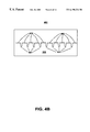
- FIG. 4A shows a down view of an enlarged portion of a polishing pad.
- FIG. 4B shows a side view of the enlarged portion of the polishing pad from FIG. 4 A.
- FIG. 5A shows a side view of an enlarged portion of a polishing pad subsequent to conditioning by a conditioner assembly.
- FIG. 5B shows a side view of the enlarged portion of the polishing pad from FIG. 5A subsequent to vacuum removal in accordance with the present invention.
- FIG. 6A shows a down view of a CMP machine in accordance with another embodiment of the present invention.
- FIG. 6B shows a side view of the CMP machine from FIG. 6 A.
- FIG. 7A shows a down view of a CMP machine in accordance with another embodiment of the present invention.
- FIG. 7B shows a side view of the CMP machine from FIG. 7 A.
- FIG. 8 shows a graph of the removal rate with respect to time of a CMP machine in accordance with the present invention.
- FIG. 9 shows a flow chart of the steps of a vacuum removal process in accordance with the present invention.
- CMP Chemical-mechanical polishing
- the CMP process involves removing all, or a portion of, a layer of dielectric material using mechanical contact between the wafer and a moving polishing pad saturated with a polishing slurry. Polishing through the CMP process flattens out height differences, since high areas of topography (hills) are removed faster than areas of low topography (valleys).
- the CMP process has the capability of smoothing out topography over millimeter scale planarization distances, leading to maximum angles of much less than one degree after polishing.
- the present invention is a vacuum removal system for removing polishing by-products from the surface of a polishing pad in a CMP machine used to polish wafers.
- the vacuum removal system includes a vacuum removal nozzle which is adapted to dislodge and remove polishing byVLSI product particles from a textured surface of a polishing pad through the application of suction.
- the vacuum removal nozzle is connected to a mounting attachment.
- the mounting attachment is mounted on the polishing machine and is adapted to maintain close proximity of the vacuum removal nozzle with the textured surface of the polishing pad.
- a vacuum line is connected to the vacuum nozzle to convey a vacuum to the vacuum nozzle and to receive the polishing by-product particles from the vacuum nozzle.
- a vacuum source is connected to the vacuum line to generate the vacuum used by the system.
- the present invention improves the performance of the polishing pad by removing the polishing by-product particles from the textured surface of the polishing pad. In so doing, a higher removal rate is achieved over a longer period of time.
- the vacuum removal system of the present invention in addition, increases the period of time a polishing pad may be utilized in the CMP machine before incurring a time consuming down time for polishing pad change out.
- the vacuum removal system of the present invention and its benefits are described in greater detail below.
- FIG. 3A shows a down view
- FIG. 3B shows a side view of a CMP machine 300 in accordance with one embodiment of the present invention.
- the CMP machine 300 picks up wafers with an arm 301 and places them onto rotating polishing pad 302 .
- the polishing pad 302 is made of a resilient material and is textured typically with a plurality of groves or pits 303 to aid the polishing process.
- the polishing pad 302 , of CMP machine 300 rotates on a platen 304 , or turn table located beneath the polishing pad 302 , at a predetermined speed.
- the arm 301 forces a wafer 311 into the polishing pad 302 with a predetermined amount of down force.
- the wafer 311 is held in place on the polishing pad 302 and the arm 301 by a carrier ring 312 and a carrier film 306 .
- the lower surface of the wafer 311 rests against the polishing pad 302 .
- the upper surface of the wafer 311 is against the lower surface of the carrier film 306 of the arm 301 .
- the CMP machine 300 also includes a slurry dispense arm 307 extending across the radius of the polishing pad 302 .
- the slurry dispense arm 307 dispenses a flow of slurry onto the polishing pad 302 .
- a conditioner assembly 308 including an end effector 309 and a conditioner arm 313 , extends across the radius of the polishing pad 302 .
- the end effector 309 includes an abrasive conditioning disk 310 which is used to roughen surface of the polishing pad 302 , in the manner described above.
- a vacuum removal nozzle 320 is mounted on CMP machine 300 by a mounting attachment 321 .
- the vacuum removal nozzle 320 extends across the radius of the polishing pad 302 and is held in close proximity with the surface of polishing pad 302 by mounting attachment 321 , such that as the polishing pad 302 rotates, the vacuum removal nozzle 320 covers nearly the entire surface of polishing pad 302 .
- the nozzle 320 is adapted to employ suction to the surface of the polishing pad 302 in order to dislodge and remove polishing by-product particles from the surface of the polishing pad 302 .
- a vacuum line 322 is connected to the vacuum removal nozzle 320 and to a vacuum source 323 , such that the vacuum line 322 conveys a vacuum generated by the vacuum source 323 to the vacuum removal nozzle 320 .
- the vacuum line 322 also receives the polishing by-product particles removed by the vacuum removal nozzle 320 .
- the polishing by-product particles and other material removed from the surface of the polishing pad are, in turn, received by the vacuum source and discharged into a polishing by-product container 324 .
- the polishing platen 304 rotates in a clockwise direction, such that the polishing pad 302 is conditioned by the conditioner assembly 308 , is “cleansed” by the vacuum removal nozzle 320 , receives fresh slurry from the slurry dispense arm 307 , and frictionally contacts the wafer 311 , in respective order, thus ensuring optimal polishing conditions for the wafer 311 .
- the vacuum removal nozzle 320 and mounting attachment 321 there are numerous functional configurations for the vacuum removal nozzle 320 and mounting attachment 321 . As such, the present invention is equally well suited to employ differing configurations for the vacuum removal nozzle 320 and mounting attachment 321 .
- FIG. 4A shows a down view of an enlarged portion 400 of the polishing pad 302 (FIG. 3A) and FIG. 4B shows a side view of the enlarged portion 400 of the polishing pad 302 .
- Polishing pad 302 includes a plurality of preformed grooves or pits 401 (hereafter grooves 401 ) manufactured directly into the material of the polishing pad 302 .
- the grooves 401 function by transporting fresh slurry to the surface of the wafer and transporting polishing by-products away from the surface of the wafer. As slurry saturates the polishing pad 302 , the grooves 401 become filled with slurry.
- the texture of the surface of the polishing pad 302 is comprised of the preformed grooves 401 and the material texture 402 .
- the lower surface of the wafer is polished by the chemical action of the slurry, e.g., chemically softening the dielectric layer, and the frictional action of the slurry abrasive particles and polishing pad texture.
- slurry is “consumed”, along with some amount of the texture of the surface of the polishing pad.
- Consumed slurry and polishing by-products in a similar manner, also adhere to the texture of the polishing pad and are transported away from the surface of the wafer.
- fresh slurry is continually dispensed onto the polishing pad from the slurry dispense arm.
- the polishing action of the slurry filling and adhering to the grooves 401 and the material texture 402 determines the removal rate and removal rate uniformity, and thus, the effectiveness of the CMP process. As slurry is consumed, the transport of fresh slurry to the surface of the wafer and the removal of polishing by-product particles away from the surface of the wafer becomes very important in maintaining the removal rate.
- the present invention ensures the grooves 401 and the material texture 402 remain clear of polishing by-product particles, and are thus fully able to transport slurry.
- FIG. 5A shows a side view of the enlarged portion 400 of the polishing pad 302 subsequent to conditioning by the conditioner assembly 308 .
- the conditioner assembly re-roughens the surface of the polishing pad in the manner described above.
- the abrasive action of the conditioner produces debris comprised of particles of polishing pad material.
- the particles of polishing pad material, particles of dielectric material from the wafer, particles of consumed slurry, and the like subsequently clog the predetermined grooves 401 and reduce their ability to transport slurry, thereby, adversely impacting the removal rate.
- the vacuum removal nozzle 320 (FIG. 3B) of the present invention dislodges and removes the by-product particles 503 through the application of suction to the surface of the polishing pad 302 .
- FIG. 5B shows a side view of the enlarged portion 400 of the polishing pad 302 subsequent to vacuum removal in accordance with the present invention.
- the by-product particles 503 have been removed from the predetermined grooves 401 and the material texture by the suction effect of the vacuum removal nozzle 320 .
- spent slurry has also been removed.
- the predetermined grooves 401 and the material texture 402 are subsequently saturated by fresh slurry from the slurry dispense arm prior to contact with the wafer.
- FIG. 6A shows a CMP machine 600 in accordance with another embodiment of the present invention.
- FIG. 6B shows a side view of the CMP machine 600 .
- the vacuum removal nozzle is comprised of a plurality of fixed vacuum ports 620 mounted on the conditioner arm 313 .
- the fixed vacuum ports are adapted to maintain close proximity with the surface of the polishing pad 302 . As the polishing pad 302 rotates beneath the fixed vacuum ports, the vacuum ports cover nearly the entire surface area of the polishing pad 302 .
- CMP machine 600 rotates the polishing pad 302 in a clockwise direction, thus, vacuum ports 602 are mounted on the conditioner arm 313 in such a manner as to dislodge and remove by suction polishing by-product particles from the surface of the polishing pad 302 immediately after polishing pad 302 is roughened by the abrasive disk 310 , thereby ensuring optimal polishing conditions for the wafer 311 .
- the plurality of fixed vacuum ports 620 e.g., fixed vacuum ports 620 can be mounted on slurry dispense arm 307 ).
- the present invention is equally well suited to employ differing configurations and mounting locations for the vacuum removal nozzle 620 .
- FIG. 7A shows a CMP machine 700 in accordance with yet another embodiment of the present invention.
- FIG. 7B shows a side view of the CMP machine 700 .
- the vacuum removal nozzle is comprised of a single vacuum port 720 mounted on the conditioner arm 313 , such that the vacuum port 720 follows the end effector 309 as it moves toward the center of the polishing pad 302 and away from the center.
- the vacuum port 720 is adapted to maintain close proximity with the surface of the polishing pad 302 .
- the vacuum port 720 “scans” toward and away from the center of polishing pad 302 such that the vacuum port 720 covers nearly the entire surface of polishing pad 302 .
- Vacuum port 720 follows the end effector 309 and is thus adapted to dislodge and remove by suction polishing by-product particles from the surface of the polishing pad 302 immediately after polishing pad 302 is roughened by the abrasive disk 310 , thereby ensuring optimal polishing conditions for the wafer 311 .
- the vacuum port 720 and mounting attachment 321 e.g., the vacuum removal nozzle can employ dual vacuum ports on either side of the end effector 309 ).
- the present invention is equally well suited to employ differing configurations for the vacuum port 720 .
- CMP machine 700 further includes a slurry container 701 connected to vacuum source 323 .
- Slurry container 701 is adapted to receive the slurry and polishing by-product particles removed from the polishing pad 302 .
- slurry container 701 contains the slurry and byproduct particles for recycling at a later time.
- the present invention may also employ an optional slurry recycle unit 702 , for filtering and recycling the removed slurry, either in conjunction with the slurry container 701 as shown in FIG. 7, or in place of slurry container 701 . By recycling “consumed” slurry, CMP processing cost are reduced.
- a graph 800 of the removal rate of a CMP machine in accordance with the present invention is shown with respect to time.
- the graph 800 shows three different cases of CMP processing.
- Line 801 shows the removal rate over time of a CMP machine processing a wafer without conditioning of the CMP machine's polishing pad and without vacuum removal of polishing by-product particles.
- Line 802 shows the removal rate over time of a CMP machine processing a wafer with conditioning but without vacuum removal of polishing by-product particles.
- Line 803 shows the removal rate over time of a CMP machine processing a wafer with conditioning and with vacuum removal of polishing by-product particles.
- the slurry used in the CMP machine a mixture of de ionized water and polishing agents, is designed to chemically aid the smooth and predictable planerization of the wafer.
- a constant predictable removal rate is important to the uniformity and performance of the wafer fabrication process.
- the removal rate should be expedient, yet yield precisely planerized wafers, free from surface anomalies. If the removal rate is too slow, the number of planarized wafers produced in a given period of time decreases, hurting the wafer through-put of the fabrication process.
- the removal rate (line 803 ) is maintained above a minimum “quality threshold” represented by line 804 for the longest period of time in comparison to line 802 and line 801 .
- polishing without conditioning and without vacuum removal results in rapid drop off of removal rate due to the fact that the polishing process results in a gradual erosion of the surface texture of the polishing pad.
- the erosion of the surface texture adversely impacts the rate at which slurry flows to the surface of the wafer, resulting in the rapid drop off of removal rate as successive wafers are polished.
- line 801 quickly falls below the quality threshold 804 , thereby causing a greater number of CMP machine down times for polishing pad change out.
- Polishing with conditioning but without vacuum removal, line 802 results in a less rapid drop off of removal rate in comparison to line 801 due to the fact that the gradual erosion of the surface texture of the polishing pad is counteracted by conditioning.
- the conditioner assembly roughens the surface of the polishing pad, maintaining adequate surface texture for a longer period of time.
- the abrasive action of the conditioner assembly produces by-product particles comprised of particles of polishing pad material, which clog the predetermined grooves or pits of the polishing pad, as described above. The clogging effects of these by-product particles leads to the gradual reduction in the rate of slurry flow to the wafer as successive wafers are polished.
- line 802 results in a less rapid drop off of removal rate in comparison to line 801 , however, a greater number of CMP machine down times for polishing pad change out are required in comparison to conditioning in conjunction with the vacuum removal process of the present invention, line 803 .
- line 803 results in an even less rapid drop off of removal rate in comparison to line 801 and 802 .
- the conditioner assembly roughens the surface of the polishing pad, the polishing by-product particles are dislodged and removed from the predetermined grooves or pits of the polishing pad in the manner described above.
- the vacuum removal process of the present invention eliminates the clogging effects of the by-product particles, and in so doing, eliminates the gradual reduction in the rate of slurry flow to the wafer attributable to the clogging effects.
- line 803 results in a longer “service life” of the polishing pad and longer periods of operation between time consuming down times for polishing pad change out. The longer service life has a positive effect on the fabrication through put of CMP machines in accordance with the present invention.
- CMP machines in accordance with the present invention can also employ a periodic “rinse” of the polishing pad to aid in dislodging the byproduct particles.
- the by-product particles are dislodged in this manner they are quickly removed by the suction of the vacuum removal nozzle, as opposed to merely moving from one location on the surface of the polishing pad to another.
- the vacuum removal of by-product particles reduces the amount of contamination of the wafers attributable to the adherence of by-product particles to the surface of the wafers.
- CMP processing in accordance with the present invention, line 803 maintains the stability of the removal rate for longer periods of time in comparison to line 802 and line 801 .
- the drop off in removal rate is slower and more predictable.
- Process 900 is used to polish wafers to the proper degree of planarization using the vacuum removal system of the present invention.
- the arm of the CMP machine grabs a wafer to be polished and places it onto the rotating polishing pad of the CMP machine.
- the polishing pad is previously coated with a layer of slurry.
- the slurry is dispensed from a slurry dispense arm, as described above.
- a flow of slurry containing polishing agents is dispensed onto the polishing pad. This flow of slurry maintains a coating of slurry on the polishing pad.
- step 903 the wafer is confined by the arm to the polishing pad as the polishing pad rotates. In addition to the polishing pad rotating, the wafer is rotated by the arm and the polishing process is carried out by the combined motion of both the polishing pad and the wafer. The friction of the wafer against the polishing pad, in conjunction with the action of the slurry, removes material from the wafer at a nominal removal rate.
- step 904 the polishing pad is roughened by the conditioning assembly.
- step 905 polishing by-product particles are dislodged and removed by the vacuum removal system of the present invention.
- step 906 the wafer is removed from the polishing pad when the polishing process is complete and the wafer is sufficiently planarized.
- the vacuum removal system of the present invention improves the performance of a polishing pad in a CMP machine.
- the present invention maintains a higher removal rate in a CMP machine over a longer period of time.
- the vacuum removal system of the present invention increases the period of time a polishing pad may be utilized in a CMP machine before incurring a time consuming down time for polishing pad change out.
Abstract
Description
Claims (19)
Priority Applications (1)
| Application Number | Priority Date | Filing Date | Title |
|---|---|---|---|
| US08/732,165 US6190236B1 (en) | 1996-10-16 | 1996-10-16 | Method and system for vacuum removal of chemical mechanical polishing by-products |
Applications Claiming Priority (1)
| Application Number | Priority Date | Filing Date | Title |
|---|---|---|---|
| US08/732,165 US6190236B1 (en) | 1996-10-16 | 1996-10-16 | Method and system for vacuum removal of chemical mechanical polishing by-products |
Publications (1)
| Publication Number | Publication Date |
|---|---|
| US6190236B1 true US6190236B1 (en) | 2001-02-20 |
Family
ID=24942443
Family Applications (1)
| Application Number | Title | Priority Date | Filing Date |
|---|---|---|---|
| US08/732,165 Expired - Lifetime US6190236B1 (en) | 1996-10-16 | 1996-10-16 | Method and system for vacuum removal of chemical mechanical polishing by-products |
Country Status (1)
| Country | Link |
|---|---|
| US (1) | US6190236B1 (en) |
Cited By (42)
| Publication number | Priority date | Publication date | Assignee | Title |
|---|---|---|---|---|
| US20010018318A1 (en) * | 1998-10-01 | 2001-08-30 | Dinesh Chopra | Methods and apparatuses for mechanical and chemical-mechanical planarization of microelectronic-device substrate assemblies on planarizing pads |
| US6428400B1 (en) * | 1996-11-14 | 2002-08-06 | Ebara Corporation | Drainage structure in polishing plant |
| US6497784B1 (en) * | 1998-02-11 | 2002-12-24 | International Business Machines Corporation | Semiconductor wafer edge bead removal method and tool |
| US6517414B1 (en) | 2000-03-10 | 2003-02-11 | Appied Materials, Inc. | Method and apparatus for controlling a pad conditioning process of a chemical-mechanical polishing apparatus |
| US6558238B1 (en) * | 2000-09-19 | 2003-05-06 | Agere Systems Inc. | Apparatus and method for reclamation of used polishing slurry |
| US6605159B2 (en) * | 2001-08-30 | 2003-08-12 | Micron Technology, Inc. | Device and method for collecting and measuring chemical samples on pad surface in CMP |
| US6616513B1 (en) | 2000-04-07 | 2003-09-09 | Applied Materials, Inc. | Grid relief in CMP polishing pad to accurately measure pad wear, pad profile and pad wear profile |
| US6634934B1 (en) * | 1999-11-19 | 2003-10-21 | Sony Corporation | Method for cleaning polishing tool, polishing method polishing apparatus |
| US20040038543A1 (en) * | 1997-08-20 | 2004-02-26 | Zahorik Russell C. | Methods for selective removal of material from wafer alignment marks |
| US6712678B1 (en) * | 1999-12-07 | 2004-03-30 | Ebara Corporation | Polishing-product discharging device and polishing device |
| US6773337B1 (en) * | 2000-11-07 | 2004-08-10 | Planar Labs Corporation | Method and apparatus to recondition an ion exchange polish pad |
| US20040187222A1 (en) * | 2003-03-31 | 2004-09-30 | Schuette Brian T. | Apparatus and methods for removing residual stain |
| US20050164606A1 (en) * | 2004-01-26 | 2005-07-28 | Tbw Industries Inc. | Chemical mechanical planarization process control utilizing in-situ conditioning process |
| US20050221731A1 (en) * | 2004-03-30 | 2005-10-06 | Lam Research Corporation | Polishing pad conditioning system |
| US6969307B2 (en) * | 2004-03-30 | 2005-11-29 | Lam Research Corporation | Polishing pad conditioning and polishing liquid dispersal system |
| US20060046623A1 (en) * | 2004-08-24 | 2006-03-02 | Applied Materials, Inc. | Method and apparatus for reduced wear polishing pad conditioning |
| US20060105678A1 (en) * | 2004-11-18 | 2006-05-18 | Tatsuya Kohama | Polishing apparatus and polishing method |
| US20060276111A1 (en) * | 2005-06-02 | 2006-12-07 | Applied Materials, Inc. | Conditioning element for electrochemical mechanical processing |
| US20070095677A1 (en) * | 2005-10-31 | 2007-05-03 | Applied Materials, Inc. | Electrochemical method for ecmp polishing pad conditioning |
| US20070158207A1 (en) * | 2006-01-06 | 2007-07-12 | Applied Materials, Inc. | Methods for electrochemical processing with pre-biased cells |
| US20070227902A1 (en) * | 2006-03-29 | 2007-10-04 | Applied Materials, Inc. | Removal profile tuning by adjusting conditioning sweep profile on a conductive pad |
| US20080014845A1 (en) * | 2006-07-11 | 2008-01-17 | Alpay Yilmaz | Conditioning disk having uniform structures |
| US20080092734A1 (en) * | 2006-10-07 | 2008-04-24 | Tbw Industries Inc. | Vacuum line clean-out separator system |
| CN1914004B (en) * | 2004-01-26 | 2010-06-02 | Tbw工业有限公司 | Multi-step pad conditioning method for chemical planarization |
| US20110132874A1 (en) * | 2009-12-03 | 2011-06-09 | Richard Gottscho | Small plasma chamber systems and methods |
| US20110212624A1 (en) * | 2010-02-26 | 2011-09-01 | Hudson Eric A | System, method and apparatus for plasma etch having independent control of ion generation and dissociation of process gas |
| US20140030958A1 (en) * | 2012-07-30 | 2014-01-30 | GLOBAL FOUNDRIES Singapore Pte. Ltd. | Single grooved polishing pad |
| US8999104B2 (en) | 2010-08-06 | 2015-04-07 | Lam Research Corporation | Systems, methods and apparatus for separate plasma source control |
| US9155181B2 (en) | 2010-08-06 | 2015-10-06 | Lam Research Corporation | Distributed multi-zone plasma source systems, methods and apparatus |
| US9177762B2 (en) | 2011-11-16 | 2015-11-03 | Lam Research Corporation | System, method and apparatus of a wedge-shaped parallel plate plasma reactor for substrate processing |
| CN105328562A (en) * | 2014-07-16 | 2016-02-17 | 中芯国际集成电路制造(上海)有限公司 | Chemical and mechanical grinding method |
| US9375825B2 (en) * | 2014-04-30 | 2016-06-28 | Applied Materials, Inc. | Polishing pad conditioning system including suction |
| US9449793B2 (en) | 2010-08-06 | 2016-09-20 | Lam Research Corporation | Systems, methods and apparatus for choked flow element extraction |
| US20180021911A1 (en) * | 2016-07-22 | 2018-01-25 | Disco Corporation | Grinding apparatus |
| US9967965B2 (en) | 2010-08-06 | 2018-05-08 | Lam Research Corporation | Distributed, concentric multi-zone plasma source systems, methods and apparatus |
| US10283325B2 (en) | 2012-10-10 | 2019-05-07 | Lam Research Corporation | Distributed multi-zone plasma source systems, methods and apparatus |
| US20200101580A1 (en) * | 2018-09-28 | 2020-04-02 | Taiwan Semiconductor Manufacturing Company, Ltd. | Vacuum assembly for chemical mechanical polishing |
| US11094554B2 (en) * | 2017-03-31 | 2021-08-17 | Taiwan Semiconductor Manufacturing Co., Ltd. | Polishing process for forming semiconductor device structure |
| US20220281069A1 (en) * | 2021-03-04 | 2022-09-08 | Taiwan Semiconductor Manufacturing Co., Ltd. | System and method for removing debris during chemical mechanical planarization |
| US11465256B2 (en) * | 2018-08-06 | 2022-10-11 | Ebara Corporation | Apparatus for polishing and method for polishing |
| US11642755B2 (en) | 2018-08-06 | 2023-05-09 | Ebara Corporation | Apparatus for polishing and method for polishing |
| CN117564917A (en) * | 2024-01-15 | 2024-02-20 | 北京芯美达科技有限公司 | Polycrystalline diamond polishing equipment |
Citations (4)
| Publication number | Priority date | Publication date | Assignee | Title |
|---|---|---|---|---|
| US3549439A (en) * | 1967-09-15 | 1970-12-22 | North American Rockwell | Chemical lapping method |
| US5433650A (en) * | 1993-05-03 | 1995-07-18 | Motorola, Inc. | Method for polishing a substrate |
| US5490809A (en) * | 1992-02-27 | 1996-02-13 | Oliver Design, Inc. | System and method for texturing magnetic data storage disks |
| US5584749A (en) * | 1995-01-13 | 1996-12-17 | Nec Corporation | Surface polishing apparatus |
-
1996
- 1996-10-16 US US08/732,165 patent/US6190236B1/en not_active Expired - Lifetime
Patent Citations (4)
| Publication number | Priority date | Publication date | Assignee | Title |
|---|---|---|---|---|
| US3549439A (en) * | 1967-09-15 | 1970-12-22 | North American Rockwell | Chemical lapping method |
| US5490809A (en) * | 1992-02-27 | 1996-02-13 | Oliver Design, Inc. | System and method for texturing magnetic data storage disks |
| US5433650A (en) * | 1993-05-03 | 1995-07-18 | Motorola, Inc. | Method for polishing a substrate |
| US5584749A (en) * | 1995-01-13 | 1996-12-17 | Nec Corporation | Surface polishing apparatus |
Cited By (76)
| Publication number | Priority date | Publication date | Assignee | Title |
|---|---|---|---|---|
| US6428400B1 (en) * | 1996-11-14 | 2002-08-06 | Ebara Corporation | Drainage structure in polishing plant |
| US20040038543A1 (en) * | 1997-08-20 | 2004-02-26 | Zahorik Russell C. | Methods for selective removal of material from wafer alignment marks |
| US20070207613A1 (en) * | 1997-08-20 | 2007-09-06 | Zahorik Russell C | Methods for selective removal of material from wafer alignment marks |
| US7244681B2 (en) * | 1997-08-20 | 2007-07-17 | Micron Technology, Inc. | Methods for selective removal of material from wafer alignment marks |
| US8053371B2 (en) | 1997-08-20 | 2011-11-08 | Micron Technology, Inc. | Apparatus and methods for selective removal of material from wafer alignment marks |
| US6497784B1 (en) * | 1998-02-11 | 2002-12-24 | International Business Machines Corporation | Semiconductor wafer edge bead removal method and tool |
| US6716090B2 (en) | 1998-10-01 | 2004-04-06 | Micron Technology, Inc. | Methods and apparatuses for mechanical and chemical-mechanical planarization of microelectronic-device substrate assemblies on planarizing pads |
| US6712676B2 (en) | 1998-10-01 | 2004-03-30 | Micron Technology, Inc. | Methods and apparatuses for mechanical and chemical-mechanical planarization of microelectronic-device substrate assemblies on planarizing pads |
| US6609957B2 (en) | 1998-10-01 | 2003-08-26 | Micron Technology, Inc. | Methods and apparatuses for mechanical and chemical-mechanical planarization of microelectronic-device substrate assemblies on planarizing pads |
| US20040192176A1 (en) * | 1998-10-01 | 2004-09-30 | Dinesh Chopra | Methods and apparatuses for mechanical and chemical-mechanical planarization of microelectronic-device substrate assemblies on planarizing pads |
| US6638148B2 (en) | 1998-10-01 | 2003-10-28 | Micron Technology, Inc. | Methods and apparatuses for mechanical and chemical-mechanical planarization of microelectronic-device substrate assemblies on planarizing pads |
| US6648736B2 (en) | 1998-10-01 | 2003-11-18 | Micron Technology, Inc. | Methods and apparatuses for mechanical and chemical-mechanical planarization of microelectronic-device substrate assemblies on planarizing pads |
| US6652364B2 (en) | 1998-10-01 | 2003-11-25 | Micron Technology, Inc. | Methods and apparatuses for mechanical and chemical-mechanical planarization of microelectronic-device substrate assemblies on planarizing pads |
| US6652365B2 (en) | 1998-10-01 | 2003-11-25 | Micron Technology, Inc. | Methods and apparatuses for mechanical and chemical-mechanical planarization of microelectronic-device substrate assemblies on planarizing pads |
| US6672946B2 (en) | 1998-10-01 | 2004-01-06 | Micron Technology, Inc. | Methods and apparatuses for mechanical and chemical-mechanical planarization of microelectronic-device substrate assemblies on planarizing pads |
| US20010018318A1 (en) * | 1998-10-01 | 2001-08-30 | Dinesh Chopra | Methods and apparatuses for mechanical and chemical-mechanical planarization of microelectronic-device substrate assemblies on planarizing pads |
| US6746316B2 (en) | 1998-10-01 | 2004-06-08 | Micron Technology, Inc. | Methods and apparatuses for mechanical and chemical-mechanical planarization of microelectronic-device substrate assemblies on planarizing pads |
| US6561878B2 (en) * | 1998-10-01 | 2003-05-13 | Micron Technology, Inc. | Methods and apparatuses for mechanical and chemical-mechanical planarization of microelectronic-device substrate assemblies on planarizing pads |
| US6964602B2 (en) | 1998-10-01 | 2005-11-15 | Micron Technology, Inc | Methods and apparatuses for mechanical and chemical-mechanical planarization of microelectronic-device substrate assemblies on planarizing pads |
| US6634934B1 (en) * | 1999-11-19 | 2003-10-21 | Sony Corporation | Method for cleaning polishing tool, polishing method polishing apparatus |
| US6712678B1 (en) * | 1999-12-07 | 2004-03-30 | Ebara Corporation | Polishing-product discharging device and polishing device |
| US6517414B1 (en) | 2000-03-10 | 2003-02-11 | Appied Materials, Inc. | Method and apparatus for controlling a pad conditioning process of a chemical-mechanical polishing apparatus |
| US20040033760A1 (en) * | 2000-04-07 | 2004-02-19 | Applied Materials, Inc. | Grid relief in CMP polishing pad to accurately measure pad wear, pad profile and pad wear profile |
| US6616513B1 (en) | 2000-04-07 | 2003-09-09 | Applied Materials, Inc. | Grid relief in CMP polishing pad to accurately measure pad wear, pad profile and pad wear profile |
| US6558238B1 (en) * | 2000-09-19 | 2003-05-06 | Agere Systems Inc. | Apparatus and method for reclamation of used polishing slurry |
| US6773337B1 (en) * | 2000-11-07 | 2004-08-10 | Planar Labs Corporation | Method and apparatus to recondition an ion exchange polish pad |
| US6837942B2 (en) | 2001-08-30 | 2005-01-04 | Micron Technology, Inc. | Device and method for collecting and measuring chemical samples pad surface in CMP |
| US20040033620A1 (en) * | 2001-08-30 | 2004-02-19 | Joslyn Michael J. | Device and method for collecting and measuring chemical samples pad surface in CMP |
| US6605159B2 (en) * | 2001-08-30 | 2003-08-12 | Micron Technology, Inc. | Device and method for collecting and measuring chemical samples on pad surface in CMP |
| US20040187222A1 (en) * | 2003-03-31 | 2004-09-30 | Schuette Brian T. | Apparatus and methods for removing residual stain |
| US7166014B2 (en) | 2004-01-26 | 2007-01-23 | Tbw Industries Inc. | Chemical mechanical planarization process control utilizing in-situ conditioning process |
| WO2005072332A3 (en) * | 2004-01-26 | 2006-03-16 | Tbw Ind Inc | Chemical mechanical planarization process control utilizing in-situ conditioning process |
| US20050164606A1 (en) * | 2004-01-26 | 2005-07-28 | Tbw Industries Inc. | Chemical mechanical planarization process control utilizing in-situ conditioning process |
| CN1910011B (en) * | 2004-01-26 | 2010-12-15 | Tbw工业有限公司 | Chemical mechanical planarization process control utilizing in-situ conditioning process |
| CN1914004B (en) * | 2004-01-26 | 2010-06-02 | Tbw工业有限公司 | Multi-step pad conditioning method for chemical planarization |
| US20050221731A1 (en) * | 2004-03-30 | 2005-10-06 | Lam Research Corporation | Polishing pad conditioning system |
| US6969307B2 (en) * | 2004-03-30 | 2005-11-29 | Lam Research Corporation | Polishing pad conditioning and polishing liquid dispersal system |
| US6958005B1 (en) * | 2004-03-30 | 2005-10-25 | Lam Research Corporation | Polishing pad conditioning system |
| US20060046623A1 (en) * | 2004-08-24 | 2006-03-02 | Applied Materials, Inc. | Method and apparatus for reduced wear polishing pad conditioning |
| US7210988B2 (en) | 2004-08-24 | 2007-05-01 | Applied Materials, Inc. | Method and apparatus for reduced wear polishing pad conditioning |
| US20060105678A1 (en) * | 2004-11-18 | 2006-05-18 | Tatsuya Kohama | Polishing apparatus and polishing method |
| US20090142990A1 (en) * | 2004-11-18 | 2009-06-04 | Tatsuya Kohama | Method for polishing a workpiece |
| US20060276111A1 (en) * | 2005-06-02 | 2006-12-07 | Applied Materials, Inc. | Conditioning element for electrochemical mechanical processing |
| US20070095677A1 (en) * | 2005-10-31 | 2007-05-03 | Applied Materials, Inc. | Electrochemical method for ecmp polishing pad conditioning |
| US7504018B2 (en) | 2005-10-31 | 2009-03-17 | Applied Materials, Inc. | Electrochemical method for Ecmp polishing pad conditioning |
| US20070158207A1 (en) * | 2006-01-06 | 2007-07-12 | Applied Materials, Inc. | Methods for electrochemical processing with pre-biased cells |
| US20070227902A1 (en) * | 2006-03-29 | 2007-10-04 | Applied Materials, Inc. | Removal profile tuning by adjusting conditioning sweep profile on a conductive pad |
| US20080014845A1 (en) * | 2006-07-11 | 2008-01-17 | Alpay Yilmaz | Conditioning disk having uniform structures |
| US20080092734A1 (en) * | 2006-10-07 | 2008-04-24 | Tbw Industries Inc. | Vacuum line clean-out separator system |
| US7909910B2 (en) | 2006-10-07 | 2011-03-22 | Tbw Industries Inc. | Vacuum line clean-out separator system |
| US20110132874A1 (en) * | 2009-12-03 | 2011-06-09 | Richard Gottscho | Small plasma chamber systems and methods |
| US9111729B2 (en) | 2009-12-03 | 2015-08-18 | Lam Research Corporation | Small plasma chamber systems and methods |
| US9911578B2 (en) | 2009-12-03 | 2018-03-06 | Lam Research Corporation | Small plasma chamber systems and methods |
| US9190289B2 (en) | 2010-02-26 | 2015-11-17 | Lam Research Corporation | System, method and apparatus for plasma etch having independent control of ion generation and dissociation of process gas |
| US20110212624A1 (en) * | 2010-02-26 | 2011-09-01 | Hudson Eric A | System, method and apparatus for plasma etch having independent control of ion generation and dissociation of process gas |
| US9735020B2 (en) | 2010-02-26 | 2017-08-15 | Lam Research Corporation | System, method and apparatus for plasma etch having independent control of ion generation and dissociation of process gas |
| US9967965B2 (en) | 2010-08-06 | 2018-05-08 | Lam Research Corporation | Distributed, concentric multi-zone plasma source systems, methods and apparatus |
| US9155181B2 (en) | 2010-08-06 | 2015-10-06 | Lam Research Corporation | Distributed multi-zone plasma source systems, methods and apparatus |
| US8999104B2 (en) | 2010-08-06 | 2015-04-07 | Lam Research Corporation | Systems, methods and apparatus for separate plasma source control |
| US9449793B2 (en) | 2010-08-06 | 2016-09-20 | Lam Research Corporation | Systems, methods and apparatus for choked flow element extraction |
| US9177762B2 (en) | 2011-11-16 | 2015-11-03 | Lam Research Corporation | System, method and apparatus of a wedge-shaped parallel plate plasma reactor for substrate processing |
| US9421669B2 (en) * | 2012-07-30 | 2016-08-23 | Globalfoundries Singapore Pte. Ltd. | Single grooved polishing pad |
| US20140030958A1 (en) * | 2012-07-30 | 2014-01-30 | GLOBAL FOUNDRIES Singapore Pte. Ltd. | Single grooved polishing pad |
| US10283325B2 (en) | 2012-10-10 | 2019-05-07 | Lam Research Corporation | Distributed multi-zone plasma source systems, methods and apparatus |
| US9375825B2 (en) * | 2014-04-30 | 2016-06-28 | Applied Materials, Inc. | Polishing pad conditioning system including suction |
| CN105328562A (en) * | 2014-07-16 | 2016-02-17 | 中芯国际集成电路制造(上海)有限公司 | Chemical and mechanical grinding method |
| US20180021911A1 (en) * | 2016-07-22 | 2018-01-25 | Disco Corporation | Grinding apparatus |
| US10343248B2 (en) * | 2016-07-22 | 2019-07-09 | Disco Corporation | Grinding apparatus |
| US11094554B2 (en) * | 2017-03-31 | 2021-08-17 | Taiwan Semiconductor Manufacturing Co., Ltd. | Polishing process for forming semiconductor device structure |
| US11465256B2 (en) * | 2018-08-06 | 2022-10-11 | Ebara Corporation | Apparatus for polishing and method for polishing |
| US11642755B2 (en) | 2018-08-06 | 2023-05-09 | Ebara Corporation | Apparatus for polishing and method for polishing |
| US20200101580A1 (en) * | 2018-09-28 | 2020-04-02 | Taiwan Semiconductor Manufacturing Company, Ltd. | Vacuum assembly for chemical mechanical polishing |
| US10843307B2 (en) * | 2018-09-28 | 2020-11-24 | Taiwan Semiconductor Manufacturing Company, Ltd. | Vacuum assembly for chemical mechanical polishing |
| US20220281069A1 (en) * | 2021-03-04 | 2022-09-08 | Taiwan Semiconductor Manufacturing Co., Ltd. | System and method for removing debris during chemical mechanical planarization |
| CN117564917A (en) * | 2024-01-15 | 2024-02-20 | 北京芯美达科技有限公司 | Polycrystalline diamond polishing equipment |
| CN117564917B (en) * | 2024-01-15 | 2024-04-02 | 北京芯美达科技有限公司 | Polycrystalline diamond polishing equipment |
Similar Documents
| Publication | Publication Date | Title |
|---|---|---|
| US6190236B1 (en) | Method and system for vacuum removal of chemical mechanical polishing by-products | |
| US6241587B1 (en) | System for dislodging by-product agglomerations from a polishing pad of a chemical mechanical polishing machine | |
| US5645469A (en) | Polishing pad with radially extending tapered channels | |
| KR100566787B1 (en) | Semiconductor polishing method and apparatus | |
| US5860181A (en) | Method of and apparatus for cleaning workpiece | |
| KR100666664B1 (en) | Polishing apparatus | |
| US6139428A (en) | Conditioning ring for use in a chemical mechanical polishing machine | |
| US6346032B1 (en) | Fluid dispensing fixed abrasive polishing pad | |
| US20020137436A1 (en) | System and method for controlled polishing and planarization of semiconductor wafers | |
| KR20030066796A (en) | System and method for polishing and planarization of semiconductor wafers using reduced surface area polishing pads | |
| JP2003229393A (en) | Combination of slurry dispenser and rinse arm, and its operating method | |
| EP0816017A1 (en) | Method and apparatus for dressing polishing cloth | |
| US6506098B1 (en) | Self-cleaning slurry arm on a CMP tool | |
| JP2002540623A (en) | Semiconductor wafer cleaning apparatus and method | |
| US6347979B1 (en) | Slurry dispensing carrier ring | |
| JPH10202507A (en) | Device and method for chemical-mechanical polishing (cmp) | |
| WO2001031691A1 (en) | Method and apparatus for cleaning a semiconductor wafer | |
| US6022265A (en) | Complementary material conditioning system for a chemical mechanical polishing machine | |
| EP1144155B1 (en) | Ultrasonic transducer slurry dispenser | |
| KR20000019355A (en) | Cmp apparatus and driving method thereof | |
| EP1156903B1 (en) | Apparatus for performing chemical-mechanical planarization | |
| EP1358046A1 (en) | Non-slip polisher head backing film | |
| JP3528501B2 (en) | Semiconductor manufacturing method | |
| JP2003220554A (en) | Polishing apparatus and polishing method for material to be polished using the same | |
| US6368968B1 (en) | Ditch type floating ring for chemical mechanical polishing |
Legal Events
| Date | Code | Title | Description |
|---|---|---|---|
| AS | Assignment |
Owner name: VLSI TECHNOLOGY, INC., CALIFORNIA Free format text: ASSIGNMENT OF ASSIGNORS INTEREST;ASSIGNOR:DRILL, CHARLES FRANKLIN;REEL/FRAME:008267/0671 Effective date: 19961014 |
|
| STCF | Information on status: patent grant |
Free format text: PATENTED CASE |
|
| FPAY | Fee payment |
Year of fee payment: 4 |
|
| FPAY | Fee payment |
Year of fee payment: 8 |
|
| AS | Assignment |
Owner name: NXP B.V., NETHERLANDS Free format text: ASSIGNMENT OF ASSIGNORS INTEREST;ASSIGNOR:PHILIPS SEMICONDUCTORS INC.;REEL/FRAME:022973/0239 Effective date: 20090715 Owner name: PHILIPS SEMICONDUCTORS VLSI INC., NEW YORK Free format text: CHANGE OF NAME;ASSIGNOR:VLSI TECHNOLOGY, INC.;REEL/FRAME:022973/0248 Effective date: 19990702 Owner name: PHILIPS SEMICONDUCTORS INC., NEW YORK Free format text: CHANGE OF NAME;ASSIGNOR:PHILIPS SEMICONDUCTORS VLSI INC.;REEL/FRAME:022973/0254 Effective date: 19991229 |
|
| FPAY | Fee payment |
Year of fee payment: 12 |