US6208006B1 - Thin film spatial filters - Google Patents
Thin film spatial filters Download PDFInfo
- Publication number
- US6208006B1 US6208006B1 US09/120,253 US12025398A US6208006B1 US 6208006 B1 US6208006 B1 US 6208006B1 US 12025398 A US12025398 A US 12025398A US 6208006 B1 US6208006 B1 US 6208006B1
- Authority
- US
- United States
- Prior art keywords
- filter
- spatial
- thin film
- spatial filter
- frequency
- Prior art date
- Legal status (The legal status is an assumption and is not a legal conclusion. Google has not performed a legal analysis and makes no representation as to the accuracy of the status listed.)
- Expired - Lifetime
Links
Images


Classifications
-
- H—ELECTRICITY
- H01—ELECTRIC ELEMENTS
- H01L—SEMICONDUCTOR DEVICES NOT COVERED BY CLASS H10
- H01L27/00—Devices consisting of a plurality of semiconductor or other solid-state components formed in or on a common substrate
-
- H—ELECTRICITY
- H10—SEMICONDUCTOR DEVICES; ELECTRIC SOLID-STATE DEVICES NOT OTHERWISE PROVIDED FOR
- H10K—ORGANIC ELECTRIC SOLID-STATE DEVICES
- H10K19/00—Integrated devices, or assemblies of multiple devices, comprising at least one organic element specially adapted for rectifying, amplifying, oscillating or switching, covered by group H10K10/00
Definitions
- This invention relates to solid state electronic devices. More particularly, it concerns thin film spatial filters made from organic or inorganic semiconductors or conductors which function as an active resistive network and find utility as spatial frequency filters to provide background suppression and local contrast gain control.
- Spatial frequency filtering is essential to a variety of image processing applications. Spatial frequency filtering is currently being used for image enhancement in medical imagery, such as in Positron Emission Tomography (PET) and Magnetic Resonance Imaging (MRI), as an aid to detection of cancerous regions. In military applications, spatial frequency filtering is useful in the arena of target detection. In this case, bandpass filtering can be used to isolate features of a given dimension from an image, thus facilitating greatly the target detection algorithms.
- PET Positron Emission Tomography
- MRI Magnetic Resonance Imaging
- the lateral conductance between pixels is emulated by a complicated multiple FET circuit, which requires a large unit cell area (“real estate”) for each pixel; typically dimensions of nearly 100 ⁇ m ⁇ 100 ⁇ m are required. Because there is such a large real estate demand for this implementation, large format arrays (e.g. 1024 ⁇ 1024) cannot be fabricated, since the resultant array would have dimensions of 10 cm ⁇ 10 cm. Current semiconductor processing techniques are not compatible with devices larger than 2 cm.
- the discrete FET implementation also has a slow time response ( ⁇ 100 msec), in addition to large power requirements (>20W for a 1024 ⁇ 1024), both of which are incompatible with real time remote sensing applications which require sub-millisecond response with sub-Watt power consumption.
- the present invention provides thin film spatial filters (TF Spatial Filters).
- TF Spatial Filters This type of device, made from layers of thin film conductors (either conducting polymers, organic conductors, or inorganic conductors or semiconductors), functions as an active resistive network.
- the nondelineated conducting layer(s) provide spatial frequency filtering including background suppression and local contrast gain control.
- a single device with simple user adjustment can function as either a high pass or low pass spatial frequency filter with frame to frame agility. Any admixture of the filtering action by a linear combination with the original image is likewise easily controlled and implemented.
- the simplifications in the device architecture enable a super-architecture of image processors that can perform a variety of complex functions. By combining several devices operated individually as high and low pass spatial filters with different blurring lengths (spatial frequency roll-off), an agile band pass spatial filter of any selected width can be constructed.
- a non-delineated array constructed from either conducting polymers or inorganic semiconductors offers both fabrication advantages and a significant saving of “real estate” within the unit cell of each pixel compared to the discrete approach implemented in conventional VLSI silicon technology [as described, for example, by C. M. Mead, Analog VLSI and Neural Systems, 1989]. This is especially true in situations where temporal signatures are to be analyzed over the entire focal plane, thereby eliminating a digital approach to lateral interaction.
- conducting polymers that are processable from solution include, but are not limited to polyaniline (emeraldine salt form) and doped poly(ethylenedioxythiophene).
- inorganic materials for the conducting layer(s) of the TF Spatial Filter.
- examples include, but are not limited to indium/tin-oxide, amorphous silicon and amorphous carbon.
- FIGS. 1A and 1B are example schematics of the TF Spatial Filter implementations.
- FIG. 1A is the TF Spatial Filter structure 10 for use in applications where the device must be grounded. In this case, the blurring is accomplished by a conducting bilayer.
- the top layer 12 comprises a low resistivity conductor material (r p ), which provides the lateral blurring required for image processing applications.
- the bottom layer 4 comprises a high resistivity layer (r b ) which prevents the top layer from shorting to ground 8 .
- FIG. 1B shows an example TF Spatial Filter structure 106 for use in applications where the device is floating (not grounded).
- the blurring is accomplished by a single conducting layer 8 which comprises a low resistivity material (r p ), which provides the lateral blurring required for image processing applications.
- variable input resistors 6 a , 6 b , 6 c , etc. one in each pixel, are ganged together to provide user tunability of the blurring length of the device (see Equation 1).
- FIG. 2 is a schematic of analog spatial frequency filtering by non-delineated resistive grids in wafer scale integration.
- the vertical axis corresponds to a particular frequency band, and the horizontal axis refers to the order of the multipole of that spectral band (i.e. the sharpness).
- FIG. 3 is a schematic of multifunctional operation of the Thin Film Spatial Filter.
- FIGS. 4A, 4 B and 4 C are a pictoral demonstration of noise reduction utility of low pass spatial frequency filter.
- FIG. 5 is an example MTF curve for a low pass filter where k is the spatial frequency, and c is an arbitrary normalizing constant.
- FIGS. 6A and 6B depict an original image ( 6 A) and the same image subjected to high pass filtering ( 6 B).
- FIG. 7 is a graph of the MTF curve for a high pass filter.
- FIGS. 8A, 8 B, 8 C, 8 D and 8 E show a demonstration of D.C. pedestal removal when using low pass filtering in conjunction with logarithmic compression: 8 A is the original image; 8 B is the original image multiplied by a continuous ramp function; 8 C is the original image multiplied by a non-abrupt step function; 8 D is the image of 8 B after application of the Mead algorithm; and 8 E is the image of 8 C after application of the Mead algorithm.
- FIG. 9 is a graphic example of a band pass MTF curve obtained by combining a low pass and high pass filter.
- FIGS. 10A, 10 B and 10 C depict band pass filtering using high pass and low pass filters in series: 10 A is the original image which is first fed into a low pass filter resulting in 10 B; 10 B output becomes the input of the high pass filter image show in 10 C.
- FIGS. 11A, 11 B, 11 C and 11 D show frequency selection using multipole filtering.
- FIG. 12 shows currents contributing to V 1 for one possible implementation of the TF Spatial Filter.
- FIG. 13 is a graphic depiction of MTF curves for the output voltage and for various blurring lengths.
- FIG. 14 is a graphic depiction of the MTF curves with the high pass filter implementation of the Thin Film Spatial Filter.
- FIG. 15 shows post-processing op amp circuitry for implementation of user control of spatial frequency filtering.
- V 1 and V in are provided from the unit cell outputs, as shown in FIG. 1 .
- FIG. 16 is a block diagram of band pass filter implementation using the Thin Film Spatial Filter.
- FIG. 17 depicts the MTF curve of a band pass filter using two Thin Film Spatial Filters.
- FIG. 18 is a block diagram of construction of a multipole filter using several Thin Film Spatial Filters.
- FIG. 19 is a graph of MTF curves of the multipole filter demonstrating the line narrowing of the band pass system.
- FIG. 20 is a graphic demonstration of tunability of multipole band pass system with a conservation of linewidth.
- FIG. 21 is the equivalent circuit of an implementation of the Thin Film Spatial Filter, for time response analysis.
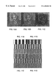
- FIG. 23 is a depiction of the shadow mask used for the 1 dimensional TF Spatial Filter fabrication.
- FIG. 24 is a plot of the resistance vs. pixel number for the TF Spatial Filter constructed with conducting PANI.
- FIG. 25 is a graph of the low pass filter response of the TF Spatial Filter to a step function input, constructed with conducting PANI.
- FIG. 26 is a plot of the resistance vs. pixel number for the TF Spatial Filter constructed with conducting PEDOT.
- FIG. 27 is a low pass filter response of the TF Spatial Filter to a step function input, constructed with conducting PEDOT.
- FIG. 28 is a plot of the resistance vs. pixel number for the TF Spatial Filter constructed with a 10% blend of PANI in a PES host.
- FIG. 29 is a graph of the low pass filter response of the TF Spatial Filter to a step function input, constructed with a 10% blend of PANI in a PES host.
- FIG. 30 is a plot of the resistance vs. pixel number for the TF Spatial Filter constructed with a 1% blend of PANI in a PES host.
- FIG. 31 is a graph of the low pass filter response of the TF Spatial Filter to a step function input, constructed with a 1% blend of PANI in a PES host.
- FIG. 32 is a plot of the resistance vs. pixel number for the TF Spatial Filter constructed with indium tin oxide (ITO).
- ITO indium tin oxide
- FIG. 33 is a graph of the low pass filter response of the TF Spatial Filter to a step function input, constructed with conducting indium tin oxide (ITO).
- ITO conducting indium tin oxide
- FIG. 34 is a plot of the resistance vs. pixel number for the TF Spatial Filter constructed with doped amorphous silicon.
- FIG. 35 is a graph of the low pass filter response of the TF Spatial Filter to a step function input, constructed with doped amorphous silicon.
- FIG. 36 is a graph of the high pass filter response of the TF Spatial Filter to a step function input, constructed with conducting PANI.
- FIG. 37 is a graph of the high pass filter response of the TF Spatial Filter to a step function input, constructed with conducting PEDOT.
- FIG. 38 is a graph of the high pass filter response of the TF Spatial Filter to a step function input, constructed with a 10% blend of PANI in a PES host.
- FIG. 39 is a graph of the high pass filter response of the TF Spatial Filter to a step function input, constructed with a 1% blend of PANI in a PES host.
- FIG. 40 is a graph of the high pass filter response of the TF Spatial Filter to a step function input, constructed with indium tin oxide (ITO).
- ITO indium tin oxide
- FIG. 41 is a graph of the high pass filter response of the TF Spatial Filter to a step function input, constructed with doped amorphous silicon.
- FIGS. 42A, 42 B, 42 C and 42 D are a demonstration of multipole bandpass filtering.
- An original image ( 42 A) consisting of a random distribution of three circle sizes was subjected to multipole bandpass filtering: 42 B) single pole; 42 C) double pole; 42 D) triple pole.
- FIG. 43 is an example of a FET circuit which emulates a variable linear resistor. Voltage is applied across the V s and the V d terminals, and the effective resistance is controlled by V c .
- the Thin Film Spatial Filter (TF Spatial Filter) of this invention provides a simple solution to the drawbacks of the existing spatial frequency filtering implementations. It is a hybrid structure, which combines the strengths of analog VLSI technology with the simplicity of a continuous sheet resistance.
- TF Spatial Filter By replacing the multiple FET lateral conductance circuit (as in the Mead implementation [C. M. Mead, Analog VLSI and Neural Systems, 1989]) with a continuous semiconductor sheet, the number of FET components in the unit cell is greatly reduced, thereby reducing the required pixel area by nearly a factor of five.
- the TF Spatial Filter large format arrays can be fabricated to satisfy the heavy processing needs for high definition images.
- the reduction of the number of FET components greatly reduces the response time of these arrays, as a result of the reduction in effective lateral capacitance of the system.
- the response time for the TF Spatial Filter is below 10 ⁇ 7 seconds, implying that the processing rate is limited only by the input/output rate of the multiplexer.
- the power consumption of the TF Spatial Filter is greatly reduced relative to both computational and discrete FET implementations. This reduction results from the fact that in the TF Spatial Filter the power consumed by the array is entropy driven, i.e. power is consumed only when and where there is contrast in the input image. In contrast, the discrete approach draws significant power even under quiescent conditions. For a 256 ⁇ 256 array TF Spatial Filter, the average power consumption is expected to be ⁇ 50 mW. The reduced power consumption reflects the fact that the lateral resistance layer does not draw any quiescent (overhead) power.
- TF Spatial Filter design An important feature of the TF Spatial Filter design is the ability to select the mode of operation either as a low pass filter or as a high pass filter (or any linear combination thereof). Consequently, two of these arrays operated in series, one operated as a low pass filter and the other as a high pass filter, will function as a bandpass filter.
- bandpass spatial frequency filter a specific spatial frequency band can be selected from images; band pass spatial frequency filtering is a powerful tool for selecting features of a given dimension.
- the combination of several of these bandpass elements, each tuned to the same bandpass center frequency, enables multipole bandpass filtering, which provides improved spatial frequency discrimination away from the center frequency of the bandpass filter.
- the agility of the TF Spatial Filter of this invention is further improved by providing a variable blurring length, which translates to a control of the cutoff frequencies for the low and high pass filter operation.
- a variable blurring length which translates to a control of the cutoff frequencies for the low and high pass filter operation.
- FIG. 1 An example of the Thin Film Spatial Filter is shown schematically in FIG. 1 as 10. It is a simple thin film structure consisting of a resistive layer with an array of ganged resistors defining the pixels. Current passing through each resistor is spatially blurred by the lateral conduction afforded by the resistive layer, resulting in an output which can be tuned to either a low pass or a high pass spatial frequency filter.
- Each of the ganged “resistors” which define the pixels in FIG. 1 can be actual resistors 6 a , 6 b , 6 c etc. or they can be simple circuits (comprising FETs) that function as voltage variable resistors.
- the series resistance value can be externally controlled by changing the voltage applied to the FET circuit independently of scene content. With this external control, one can vary the decay length and thereby externally control the roll-off of the spatial frequency filter.
- N The blurring parameter (or decay length), N, is defined as the number of pixels over which the local averaging takes place, and is given by the following expression: N ⁇ R eff R L ( 1 )
- the parameters a and b refer to the width of the pixel and separation between pixels, respectively, whereas t and d correspond to the thickness of the conductive (blurring) and insulating layers.
- the blurring parameter is given by N ⁇ ⁇ ⁇ ⁇ 1 R L
- the larger vision of the potential for the TF Spatial Filter is of an analog image processing super-architecture that combines TF Spatial Filters for a variety of sophisticated functions. For example:
- Ceramic carrier modules would be ideal for the TF Spatial Filters. The fact that this is an existing technology in the semiconductor industry makes this implementation attractive.
- FIG. 2 shows a schematic representation of a possible implementation. The result is a parallel computation of non-contiguous spatial frequencies, which could be accomplished within the frame time of the focal plane readout.
- the TF Spatial Filter is a multifunctional image processing tool.
- the TF Spatial Filter can function as either a low pass or high pass spatial filter (or a linear combination thereof).
- FIG. 4 shows an airplane on a runway.
- FIG. 4 b shows the clean image (from FIG. 4 a ) with high-frequency noise superimposed, such that the signal to noise is approximately 1; the plane is difficult to detect when shrouded by this noise.
- a “blurring” function (FIG. 4 c )
- V out ⁇ V in >
- ⁇ V in > is the input image blurred over N pixels.
- the function of the blurring “algorithm” is to pass the low spatial frequencies (primarily the plane), while suppressing the high frequency information (primarily the noise).
- the sharper edges of the plane are blurred along with the undesired noise; however, the net result is an enhanced version of the noisy scene.
- the low pass spatial filter can be described by the modulation transfer function (MTF), which is a measure of the throughput of the “filter” with respect to spatial frequency,
- V out ( k ) MTF lp ( k ) V in ( k ) (2)
- the operation is a low pass filter, as shown in the schematic MTF curve plotted in FIG. 5 .
- the characteristic roll-off frequency of the low pass filter is determined by the blurring length, see equation (1); a large blurring length yields a low rolloff frequency, whereas a small blurring length yields a higher rolloff frequency.
- FIG. 6 b displays an example of such an operation on the image of Dr. Einstein shown in FIG. 6 a .
- the calculation performed on the image can be expressed as
- V out V in ⁇ V in > (3)
- Equation 3 functions as a high pass spatial filter which can also be described by a MTF as follows:
- V out ( k ) V in ( k ) ⁇ MTF lp ( k ) V in ( k ) (4)
- V out ( k ) [1 ⁇ MTF lp ( k )] V in ( k ) (5)
- MTF hp and MTF lp are the modulation transfer functions for the high pass and low pass filters, respectively.
- An example of a MTF hp is sketched in FIG. 7 which shows that features in the image below a certain spatial frequency are completely suppressed, whereas higher spatial frequency features persist.
- the rolloff frequency is controlled by the blurring length; a large blurring length yields a low rolloff frequency whereas a small blurring length yields a higher rolloff frequency.
- V in ( i ) V o logI ( i ) (7)
- V out ( i ) V o logI ( i ) ⁇ ( V o /N ) ⁇ j logI ( j ) (8)
- FIG. 8 a shows the original 8 bit image of Dr. Einstein multiplied by a ramp function which ranges from 0 on the left to 255 on the right; the new image is therefore a 16 bit grayscale image which contains all of the information from the original photo.
- the resulting images contain nearly all of the spatial content of the original photo of Dr. Einstein (with the exception of the low frequency components).
- the Mead implementation is a powerful means to providing background suppression on images with large DC pedestals.
- V out ( k ) MTF low ( k ) MTF high ( k ) V in ( k ) (10)
- the system MTF is a product of the MTFs of the individual filters.
- FIG. 9 shows schematically in FIG. 9 .
- the net result is an image whose medium frequencies are transmitted, and low/high frequency features are suppressed.
- the band pass spatial frequency can be tuned by the proper choice of the blurring lengths of the filters, as demonstrated in FIG. 10, which shows the processed image for a different choice of N and N′.
- FIG. 11 demonstrates spatial frequency selection.
- the original image consists of three sinusoidally varying patterns of grayscale, each with a different characteristic spatial frequency.
- the image is then passed through a series of band pass spatial filters, whose center frequency is tuned to the spatial frequency of the middle grayscale pattern.
- the intensity of the middle pattern remains relatively unchanged, while the higher and lower spatial frequency patterns are suppressed; after 6 iterations, the high and low frequency patterns are nearly completely removed.
- the image processing functions described above have been simulated in the software domain.
- the TF Spatial Filter of this invention is capable of implementing these processing functions in real time. With the TF Spatial Filter, these processing functions are accomplished in the analog domain by a thin film device which functions as a specialized parallel processing “computer” for image processing. This effective computation speed is equivalent to that of a supercomputer in a structure with almost unlimited restriction on array format.
- On-board digital FFT methods are too slow for the volume of data expected (for example, in hyperspectral and ultraspectral systems); and they preclude fusion prior to A/D conversion.
- the processing of large format systems at fast frame rates with many spectral images is a supercomputer computation.
- the TF Spatial Filter is fabricated with at most two layers of semiconducting materials; these layers can consist of any two materials whatsoever, as long as the conductivities of these layers are sufficiently ifferent to provide the lateral blurring function.
- the TF Spatial Filter can also be fabricated with only one layer, and will function with any material which possesses the sheet resistance uniformity required by the application.
- An important difference with the TF Spatial Filter design is the fact that the high conductivity (blurring) layer can be continuous (non-porous).
- the TF Spatial Filter allows for versatility in its function as an image filter: it can function as either a low pass or a high pass spatial frequency filter, with a simple external user control.
- the “Smart Polymer Image Processor” can only function as a high pass filter, making it an image processor of very limited utility.
- This invention describes Thin Film Spatial Filters (TF Spatial Filter).
- TF Spatial Filter Thin Film Spatial Filters
- FIG. 1 The basic structure of an implementation of the TF Spatial Filter is shown schematically in FIG. 1 as 10 and 10 b.
- FIG. 1 a shows the structure for use in applications where the device must be grounded.
- the blurring is accomplished by a conducting bilayer.
- the top layer 2 comprises of a low resistivity material (r p ), which provides the lateral blurring required for image processing applications.
- the bottom layer 4 comprises a high resistivity layer (r b ) which prevents the top layer from shorting to ground.
- the blurring number is given by N ⁇ R eff R L
- R v is the resistance associated with the variable (ganged) resistors.
- the parameters a and b refer to the width of the pixel and separation between pixels, respectively, whereas t and d correspond to the thickness of the conductive (blurring) and insulating layers.
- the blurring is accomplished by a single conducting layer 8 which comprises a low resistivity material (r p ), which provides the lateral blurring required for image processing applications.
- r p low resistivity material
- the blurring parameter is given by N ⁇ R v R L
- R v is the resistance associated with the variable (ganged) resistors
- R L ⁇ p ⁇ b ta
- the blurring length can be varied by changing r p , by changing t, or by changing the value of the series resistance in each pixel.
- the blurring parameter is given by N ⁇ ⁇ ⁇ ⁇ 1 R L
- the TF Spatial Filter comprises an x-y array of pixels each defined by a contact pad to the underlying conducting layer.
- the array could be an array of any size; for example 128 by 128, 256 by 256, 512 by 512 or 1024 by 1024.
- the series resistance circuit provides the input and the output as indicated.
- the image to be processed for example, from a corresponding array of photodetectors (for example, 128 by 128, 256 by 256, 512 by 512 or 1024 by 1024 arrays of photodetectors) is first multiplexed out of the detector array and then de-multiplexed onto the pixels of the TF Spatial Filter in one-to-one correspondence with the original image.
- the output from each pixel provides the spatially filtered version of the input image.
- the output can be multiplexed, subjected to analog-to-digital conversion and subsequently processed in digital form.
- the output is multiplexed and subsequently displayed for view, for example on a cathode ray tube, a liquid crystal display or an emissive display, or the like.
- the series resistance is the same for each of the pixels in the array (the resistors are ‘ganged’).
- the series resistance is not necessarily the same for each of the pixels in the array.
- each of the ganged “resistors” 6 which define the pixels in FIG. 1 are actual resistors.
- each of the ganged “resistors” 6 which define the pixels in FIG. 1 are simple circuits (comprising FETs) that function as voltage variable resistors.
- FETs field-effect transistors
- Using an FET circuit that functions as a series resistor is preferable, because in this case the series resistance value can be externally controlled by changing the voltage applied to the circuit. With this external control, one can vary the decay length and thereby vary the roll-off of the spatial frequency filter.
- An example of such a voltage variable resistor circuit is provided in Example 16.
- Other circuits which function as series resistors are well known in the art; all that is required is that the tuned resistance be independent of the scene dependent current draw.
- the number of FETs comprising the variable resistance circuit is minimized; the fewer the better. More FETs take up more space and thereby require larger sized pixels.
- a minimum sized pixel is preferred in order to make possible large scale x-y arrays, for example 256 by 256, 512 by 512 or 1024 by 1024.
- the Conducting Layer (or Bilayer)
- the conducting layer comprises a conducting material with resistivity r p and thickness t.
- the values of r p and t, together with the series resistance value, R s , are chosen to yield the desired decay length according to Equation 1.
- the composition of the conductive layer is not critical. Materials with stable resistivity and with dimensional stability are preferred. Since the value of the series resistance obtained with the FET circuit implementation is in the range of 10 3 ⁇ -10 8 ⁇ , the resistivity of the conducting layer should be in the range of 10 ⁇ 2 ⁇ -cm to 10 8 ⁇ -cm, with a thickness between 50 ⁇ units and 1 cm. These values will yield a blurring parameter in the range 10 ⁇ 3 to 10 3 .
- the conducting layer comprises a conducting polymer or a blend of conducting polymer with an insulating polymer.
- the resistivity of the layer can be varied by varying the volume fraction of conducting polymer in the blend.
- the conducting layer(s) of the TF Spatial Filter is fabricated from soluble conducting conjugated polymers (and/or their precursor polymers), cast from solution.
- Solution casting is simple and enables the fabrication of large active areas.
- metallic polymers that are processable from solution include, but are not limited to polyaniline (emeraldine salt form) and doped poly(ethylenedioxythiophene).
- the conducting layer can be formed by in-situ polymerization of doped material; for example, of polypyrrole, polyaniline, or polythiophene.
- Inorganic materials can also be used for the conducting layer. Examples include, amorphous silicon, indium/tin-oxide and amorphous carbon. Such materials can be formed into conducting layers by methods well known in the art. Again, the composition of the inorganic conducting layer is not critical; materials with stable resistivity and with dimensional stability are preferred. Since the value of the series resistance obtained with the FET circuit implementation is in the range of 10 3 ⁇ -10 8 ⁇ , the resistivity of the conducting layer should be in the range of 10 ⁇ 2 ⁇ -cm to 10 8 ⁇ -cm, with a thickness between 50 ⁇ units and 1 cm. These values will yield a blurring parameter in the range 10 ⁇ 3 to 10 3 .
- the single layer configuration (FIG. 1 b ) is preferred. In cases where the bilayer is required, care must be taken to ensure that the two layers comprising the bilayer remain intact with minimal intermixing.
- the input voltages are applied to the resistors R v , which results in a diffusive spreading of the currents throughout the structure.
- the output voltage can be solved using Kirchoff's Laws (FIG. 12 ):
- I l and I r are the lateral currents entering and leaving the “cube” (see FIG. 12) from layer 1
- V 1 ⁇ ( k ) R L 2 ⁇ R v [ V in ⁇ ( k ) 1 + R L 2 ⁇ R eff - cos ⁇ ⁇ ( kc ) ] ( 16 )
- MTF ⁇ ( k ) R L 2 ⁇ R v [ 1 1 + R L 2 ⁇ R eff - cos ⁇ ⁇ ( kc ) ] ( 17 )
- Equation 17 For small values of R L /R eff , Equation 17 becomes MTF ⁇ ( k ) ⁇ R L R v [ 1 ( kc ) 2 + R L R eff ] ( 18 )
- the output voltage behaves as a low pass spatial frequency filter: At low spatial frequencies (i.e. a nearly constant input spatial profile), the transmission of the “filter” is high; conversely, at large spatial frequencies, where the pixel to pixel input voltage variations are large, the transmission is significantly reduced.
- MTF lp R v R eff ⁇ MTF ⁇ ( k ) ( 21 )
- Equation 16 can be converted back to real space to yield the solution for V 1 (i):
- MTF ⁇ ( k ) R L 2 ⁇ R v [ 1 1 + R L 2 ⁇ R eff - cos ⁇ ( kc ) ] ( 28 )
- R v is by definition a variable resistor
- tuning of the rolloff frequency can be achieved by changing its value (Equations 15 and 20), as shown in FIG. 13 .
- V out ⁇ ( i ) V in ⁇ ( i ) - ⁇ V in ⁇ ⁇ ( i ) ( 30 )
- V out ⁇ ( i ) V in ⁇ ( i ) - R v R eff ⁇ V 1 ⁇ ( i ) ( 31 )
- MTF hp [ 1 - cos ⁇ ⁇ ( kc ) 1 + R L 2 ⁇ R eff - cos ⁇ ( kc ) ] ( 33 )
- the rolloff of the high pass filter is determined by Equation 20, as with its low pass counterpart. Again, tuning of this rolloff frequency is achieved by adjusting the variable resistor, R v (Equation 15).
- V out ⁇ ( i ) fV in ⁇ ( i ) - R v R eff ⁇ V 1 ⁇ ( i ) ( 34 )
- FIG. 15 A simple dual op-amp circuit that will achieve this function is shown as 150 in FIG. 15 .
- Other circuits which will accomplish this task are well known in the art.
- Equation 37 implements Equation 34, since as R c >0, f ⁇ 0, and for R c >>R, f ⁇ 1.
- R c the Thin Film Spatial Filter can be tuned to create either a high pass or a low pass filter.
- the dual Op-amp circuit of FIG. 15 does not reside in the unit cell. It is a post-processing circuit which operates on the serial stream of data after the multiplexing (MUX) operation. The only condition for successful implementation of this circuit is that the output and input voltages are synchronized correctly. This has already been included in the design, as both V in and V 1 are measured as outputs on the same clock cycle.
- MUX multiplexing
- the Thin Film Spatial Filter can be operated as either a high pass or a low pass filter (or a linear combination), it is evident that two of these devices operated in series (with a different rolloff frequency selected via R v ), one operated as a high pass and the other as a low pass filter, will implement a band pass filter.
- This system shown schematically in FIG. 16, requires the output of filter 1 to be used as the input to filter 2 .
- each N can be selected via the individual R v , tuning of the band pass frequency is readily achieved via simple external user control.
- a band pass filter 160 can be readily implemented with two TF Spatial Filters in series, one operated as a low pass and the other as a high pass filter.
- the transmission bandwidth is rather large, which is disadvantageous if one wishes to select a very narrow range of spatial frequencies.
- the transmission bandwidth can be narrowed by operating several of these band pass “blocks” in series, with each block tuned to the same spatial frequency k o , as shown as 180 in FIG. 18 .
- FIG. 19 shows the effect of such a multiplication; as the number of blocks (m) increases, the linewidth of the multipole filter is dramatically reduced.
- the linewidth of this multipole filter can be approximated by ⁇ ⁇ ⁇ ( kc ) ⁇ ln ⁇ ( 2 ) m ⁇ ( 1 N low + 1 N high ) ( 42 )
- the maximum spatial frequency one can scan also increases.
- Equation 45 the lateral capacitance has been neglected, since the array pitch is assumed to be much larger than the device thickness.
- V 1 (k,t) becomes n ⁇ ( k ) ⁇ R L 2 ⁇ R v ⁇ ( 1 1 - cos ⁇ ( kc ) + R L 2 ⁇ R eff ) ⁇ ⁇ ⁇ 1 - exp [ - 2 ⁇ t ⁇ RC ⁇ ( 1 - cos ⁇ ( kc ) ( 49 )
- Equation 49 R L 2 ⁇ R v ⁇ ( 1 1 - cos ⁇ ( kc ) + 1 2 ⁇ N eff 2 ) ⁇ ⁇ 1 - exp [ - 2 ⁇ t ⁇ RC ⁇ ( 1 - cos ⁇ ( kc ) + ( 50 )
- FIG. 22 shows the time evolution of Equation 50; as t becomes very large, the MTF approaches that of Equation 17.
- R eff is a function of R v
- the maximum relaxation time will change when the variable resistor is changed by the user.
- R eff ⁇ 100 k ⁇ , C 1 , C v ⁇ 1 pF, which results in a maximum relaxation time (t rel ) max ⁇ 1 ⁇ 10 ⁇ 7 s. Therefore the maximum theoretical frame rate for the Thin Film Spatial Filter is enormous. This implies that spatial frequency scanning by the generation of sequential multipole filters can be accomplished within the frame time of the detector readout.
- One-dimensional single layer Thin Film Spatial Filters were fabricated with conducting polyaniline camphor sulfonic acid (PANI-CSA) spin cast onto a substrate with pre patterned Au electrodes. Onto a glass substrate was thermally deposited a series of 1000 ⁇ thick Au (with a 50 ⁇ adhesion layer) electrodes, using the fan out pattern shown in FIG. 23 .
- the electrode width was 100 ⁇ m, with a separation between adjacent electrodes of 400 ⁇ m.
- a 2.5% solution (in m-cresol) of conducting PANI-CSA was spin cast onto the substrate (with electrodes) at 4000 rpm, at 25° C., resulting in a film thickness of approximately 500 ⁇ [details about the preparation of the polyaniline (PANI) solution and PANI-CSA film have been disclosed in U.S. Pat. No. 5,232,631 which is herein incorporated by reference].
- the cast films were baked at 85° C. in a vacuum oven for 12 hours in order to remove any excess solvent.
- the voltage source was a Elenco Precision Quad Power Supply. This source was used to supply a variety of input profiles to the TF Spatial Filter.
- FIG. 24 demonstrates the pixel to pixel uniformity of the lateral resistance for the TF Spatial Filter.
- the resistance between pixel 1 and pixels 2 - 13 were measured (without R v ).
- the data follow very closely a straight line, indicating a highly uniform sheet resistance for the PANI-CSA layer.
- FIG. 25 shows the response of the TF Spatial Filter, operated as a low pass filter (i.e. output taken as V 1 ) to an input step function, with a voltage of 2.46 Volts applied to pixels 1 - 7 , and pixels 8 - 14 grounded.
- Each curve represents a different value of the ganged resistors, R v , ranging from 51 ⁇ up to 10k ⁇ . It is clear that at the lowest value of R v , the response curve of the device (a low pass filter) follows very closely the input function, indicating a very short decay parameter for the system ( ⁇ 0.75), consistent with Equation 1.
- the system response curve becomes nearly constant, and is essentially the global average of all of the input voltages; the spatial decay parameter in this case is very large ( ⁇ 10).
- the Thin Film Spatial Filter operated in this mode is a low pass spatial frequency filter, since the input image (profile) is blurred, with sharp (high frequency) features suppressed.
- TF Spatial Filters can be constructed using PANI-CSA films cast from solution, and that these devices operate as low pass spatial frequency filters.
- the desired cutoff frequency can be adjusted by changing the ganged resistor, which indicates the strong versatility of the TF Spatial Filter.
- the 500 ⁇ thickness for the thin film is representative. Suitable thickness for the conductive and resistive film range from as little as 50 ⁇ to as much as 10,000 ⁇ or more with thicknesses in the range of 75 ⁇ to 5,000 ⁇ being very typical.
- FIG. 27 shows the response of the low pass filter operation of the TF Spatial Filter (constructed with PEDOT) to an input step function of 2.46 Volts. The behavior was identical to that presented in example 1, with the low R v values giving rise to a short decay parameter, and the higher R v values yielding a longer spatial decay parameter.
- PEDOT conducting polymer poly(ethylenedioxythiophene)
- FIG. 29 shows the response of the low pass filter operation of the TF Spatial Filter (constructed with a 10% polyaniline/polyethylenesulfonate (PANI/PES) blend) to an input step function of 2.46 Volts. The behavior was identical to that presented in example 1, with the low R v values giving rise to a short decay parameter, and the higher R v values yielding a longer spatial decay parameter.
- FIG. 31 shows the response of the low pass filter operation of the TF Spatial Filter (constructed with a 1% PANI/PES blend) to an input step function of 2.46 Volts. The behavior was identical to that presented in example 1, with the low R v values giving rise to a short decay parameter, and the higher R v values yielding a longer spatial decay parameter.
- ITO indium tin oxide
- a glass substrate (initially uniformly coated with ITO, with a sheet resistance of 1000 ⁇ /square) was photolithographically patterned to produce a 1 cm ⁇ 0.5 cm square of ITO.
- Al electrodes were then thermally deposited onto the ITO squares using the shadow mask design shown in FIG. 23 .
- FIG. 32 demonstrates the pixel to pixel uniformity of the lateral resistance for the TF Spatial Filter.
- the resistance between pixel 1 and pixels 2 - 13 were measured (without R v ).
- the data follows very closely a straight line, indicating a highly uniform sheet resistance for the ITO layer.
- FIG. 33 shows the response of the low pass filter operation of the TF Spatial Filter (constructed with ITO) to an input step function of 2.46 Volts.
- the behavior was identical to that presented in example 1, with the low R v values giving rise to a short decay parameter, and the higher R v values yielding a longer spatial decay parameter.
- One-dimensional single layer Thin Film Spatial Filters were fabricated with doped amorphous silicon layers.
- a silicon substrate (initially uniformly coated with amorphous silicon and a SiO 2 buffer layer, with a sheet resistance of 900 ⁇ /square) was photolithographically patterned to produce a 1 cm ⁇ 0.5 cm square of amorphous Si.
- Al electrodes were then thermally deposited onto the ITO squares using the shadow mask design shown in FIG. 23 .
- FIG. 34 demonstrates the pixel to pixel uniformity of the lateral resistance for the TF Spatial Filter.
- the resistance between pixel 1 and pixels 2 - 13 were measured (without R v ).
- the data follows very closely a straight line, indicating a highly uniform sheet resistance for the amorphous silicon layer.
- FIG. 35 shows the response of the low pass filter operation of the TF Spatial Filter (constructed with amorphous silicon) to an input step function of 2.46 Volts.
- the behavior was identical to that presented in example 1, with the low R v values giving rise to a short decay parameter, and the higher R v values yielding a longer spatial decay parameter.
- the device described in example 1 was operated as a high pass spatial frequency filter. This was achieved by measuring the voltage across each pixel in the array, yielding V in (i) ⁇ V in (i)>, the required output for a high pass filter.
- FIG. 36 shows the response of the TF Spatial Filter, operated as a high pass filter (i.e. output taken as V in ⁇ V 1 ) to an input step function. It is clear that at the lowest value of R v , the response curve of the device (a high pass filter in this case) shows very narrow spikes on either side of pixel 7 , indicating a very short decay parameter for the system (large spatial cutoff frequency), consistent with Equation 1; in this case only the highest spatial frequencies are passed in the image.
- the system response showed elongated spikes near pixel 7 , indicating a very large spatial decay parameter (low spatial cutoff frequency); in contrast to the lowest R v curve, more low frequency components are transmitted in this case.
- the Thin Film Spatial Filter operated in this mode is a high pass spatial frequency filter, with low frequency features suppressed.
- FIG. 37 shows the response of the high pass filter operation of the TF Spatial Filter (constructed with PEDOT) to an input step function of 2.46 Volts.
- the behavior was identical to that presented in example 7, with the low R v values giving rise to a short decay parameter, and the higher R v values yielding a longer spatial decay parameter.
- FIG. 38 shows the response of the high pass filter operation of the TF Spatial Filter (constructed with 10% PANI/PES blends) to an input step function of 2.46 Volts. The behavior was identical to that presented in example 7, with the low R v values giving rise to a short decay parameter, and the higher R v values yielding a longer spatial decay parameter.
- FIG. 39 shows the response of the high pass filter operation of the TF Spatial Filter (constructed with 1% PANI/PES blends) to an input step function of 2.46 Volts. The behavior was identical to that presented in example 7, with the low R v values giving rise to a short decay parameter, and the higher R v values yielding a longer spatial decay parameter.
- FIG. 40 shows the response of the high pass filter operation of the TF Spatial Filter (constructed with ITO) to an input step function of 2.46 Volts. The behavior was identical to that presented in example 7, with the low R v values giving rise to a short decay parameter, and the higher R v values yielding a longer spatial decay parameter.
- FIG. 41 shows the response of the high pass filter operation of the TF Spatial Filter (constructed with amorphous silicon) to an input step function of 2.46 Volts. The behavior was identical to that presented in example 7, with the low R v values giving rise to a short decay parameter, and the higher R v values yielding a longer spatial decay parameter.
- Examples 1-6 demonstrated the operation of 1-dimensional TF Spatial Filters as low pass spatial frequency filters, constructed with a variety of material bases, and that the behavior of these devices was consistent with theoretical analysis.
- computer simulations of the TF Spatial Filter, operated as a low pass spatial frequency filter, were performed on the Einstein photo shown in FIG. 10 a.
- the initial image was a 256 ⁇ 256 grayscale picture, with 8 bits per pixel resolution.
- the computer algorithm involved the solution to the two dimensional version of equation 14, with the input “voltages” (ranging from 0-255) provided by the original image.
- a Gauss-Sidel iteration method [R. L. Burden, Numerical Analysis, 1985] was used to solve the resultant 256 2 ⁇ 256 2 matrix, with an error tolerance of 0.01.
- the result of the TF Spatial Filter low pass operation is shown in FIG. 10 b .
- the spatial decay parameter, N (equation 1), was chosen to be 2.3, which provided a moderate blurring action.
- N Equation 1
- This example demonstrates, via computer simulation, the utility of the 2 dimensional TF Spatial Filter as a low pass spatial frequency filter.
- the behavior is consistent with both the 1 dimensional fabricated structures and the theoretical analysis.
- Examples 7-12 demonstrated the operation of 1-dimensional TF Spatial Filters as high pass spatial frequency filters, constructed with a variety of material bases, and that the behavior of these devices was consistent with theoretical analysis.
- computer simulations of the TF Spatial Filter, operated as a high pass spatial frequency filter, were performed on the Einstein photo shown in FIG. 6 a.
- the result of the TF Spatial Filter high pass operation is shown in FIG. 6 b .
- the spatial decay parameter, N (equation 1), was chosen to be 2.3, which provided a moderate blurring action.
- N Equation 1
- This example demonstrates, via computer simulation, the utility of the 2 dimensional TF Spatial Filter as a high pass spatial frequency filter.
- the behavior is consistent with both the 1 dimensional fabricated structures and the theoretical analysis.
- Examples 1-14 demonstrated the operation of the TF Spatial Filter as either a low pass or high pass spatial frequency filter.
- This example demonstrates two TF Spatial Filters can be combined to create a band pass spatial filter, with one device operated as a low pass and the other as a high pass spatial frequency filter.
- the center frequency of the resulting band pass filter is determined by the spatial decay parameters of the individual filters, and is therefore tunable, by virtue of examples 1-12.
- Example 15 demonstrated that two TF spatial filters can be combined to produce a band pass spatial frequency filter.
- computer simulations were used to implement multipole band pass spatial frequency filtering. This was achieved by repeating the band pass filtering operation described in example 15, with each band pass “block” (FIG. 18) tuned to the same center frequency.
- FIG. 11 demonstrates an example of multipole bandpass spatial frequency filtering, used for feature selection.
- the original image (FIG. 11 a ), which consisted of three sinusoidally varying grayscale patterns, was subjected to multipole bandpass spatial frequency filtering (via simulation). The center frequency of this filter was tuned to the frequency of the middle pattern. After only 4 passes (poles), the low and high frequency patterns were suppressed, whereas the medium frequency pattern was enhanced; after 6 poles, the low and high frequency patterns were nearly eliminated from the image.
- Multipole bandpass spatial frequency filtering was also used to isolate image features (as opposed to patterns) in a 2 dimensional image.
- FIG. 42 shows the result of multipole bandpass spatial frequency filtering on a grayscale image with a random distribution of three sizes of circles. The bandpass filter was tuned to a region of the spatial frequency domain where the spectral density of the smallest circles was large. After only 3 poles, the medium and large circles are nearly eliminated.
- FIG. 43 An example of a variable resistor implemented using a small number of FETs is shown in FIG. 43 [R. Gregorian, Analog MOS Integrated Circuits for Signal Processing , Wiley, 1986].
- Transistors Q 1 and Q 4 , Q 2 and Q 5 , Q 3 and Q 6 are assumed to be matched components.
- V DD is an external bias (for proper circuit operation)
- V c is the control bias, allowing for an external control of the circuit resistance value; the input is applied across the S and D terminals.
Abstract
Description


Claims (18)
Priority Applications (1)
| Application Number | Priority Date | Filing Date | Title |
|---|---|---|---|
| US09/120,253 US6208006B1 (en) | 1997-07-21 | 1998-07-21 | Thin film spatial filters |
Applications Claiming Priority (2)
| Application Number | Priority Date | Filing Date | Title |
|---|---|---|---|
| US5357297P | 1997-07-21 | 1997-07-21 | |
| US09/120,253 US6208006B1 (en) | 1997-07-21 | 1998-07-21 | Thin film spatial filters |
Publications (1)
| Publication Number | Publication Date |
|---|---|
| US6208006B1 true US6208006B1 (en) | 2001-03-27 |
Family
ID=21985182
Family Applications (1)
| Application Number | Title | Priority Date | Filing Date |
|---|---|---|---|
| US09/120,253 Expired - Lifetime US6208006B1 (en) | 1997-07-21 | 1998-07-21 | Thin film spatial filters |
Country Status (4)
| Country | Link |
|---|---|
| US (1) | US6208006B1 (en) |
| EP (1) | EP1016144A4 (en) |
| AU (1) | AU8502598A (en) |
| WO (1) | WO1999004438A1 (en) |
Cited By (3)
| Publication number | Priority date | Publication date | Assignee | Title |
|---|---|---|---|---|
| US20030184739A1 (en) * | 2002-03-28 | 2003-10-02 | Kla-Tencor Technologies Corporation | UV compatible programmable spatial filter |
| US6847025B1 (en) * | 1998-10-30 | 2005-01-25 | Riken | Semiconductor image position sensitive device |
| US20100089443A1 (en) * | 2008-09-24 | 2010-04-15 | Massachusetts Institute Of Technology | Photon processing with nanopatterned materials |
Citations (5)
| Publication number | Priority date | Publication date | Assignee | Title |
|---|---|---|---|---|
| US5130775A (en) | 1988-11-16 | 1992-07-14 | Yamatake-Honeywell Co., Ltd. | Amorphous photo-detecting element with spatial filter |
| US5232631A (en) | 1991-06-12 | 1993-08-03 | Uniax Corporation | Processible forms of electrically conductive polyaniline |
| US5315100A (en) | 1991-11-19 | 1994-05-24 | Yamatake-Honeywell Co., Ltd. | Photoelectric conversion apparatus for detecting movement of object with spatial filter electrode |
| US5323208A (en) * | 1992-03-09 | 1994-06-21 | Hitachi, Ltd. | Projection exposure apparatus |
| US5804836A (en) | 1995-04-05 | 1998-09-08 | Uniax Corporation | Smart polymer image processor |
Family Cites Families (5)
| Publication number | Priority date | Publication date | Assignee | Title |
|---|---|---|---|---|
| JPH02250474A (en) * | 1989-03-24 | 1990-10-08 | Hitachi Ltd | Solid-state image pickup element |
| JPH03253075A (en) * | 1990-03-02 | 1991-11-12 | Hitachi Ltd | Solid-state image sensing element |
| DE4337160C2 (en) * | 1993-10-30 | 1995-08-31 | Daimler Benz Aerospace Ag | Photodetector array and method for its operation |
| US5567957A (en) * | 1995-01-03 | 1996-10-22 | Xerox Corporation | Segmented resistance layers with storage nodes |
| US5629517A (en) * | 1995-04-17 | 1997-05-13 | Xerox Corporation | Sensor element array having overlapping detection zones |
-
1998
- 1998-07-21 AU AU85025/98A patent/AU8502598A/en not_active Abandoned
- 1998-07-21 EP EP98935856A patent/EP1016144A4/en not_active Withdrawn
- 1998-07-21 WO PCT/US1998/015029 patent/WO1999004438A1/en not_active Application Discontinuation
- 1998-07-21 US US09/120,253 patent/US6208006B1/en not_active Expired - Lifetime
Patent Citations (5)
| Publication number | Priority date | Publication date | Assignee | Title |
|---|---|---|---|---|
| US5130775A (en) | 1988-11-16 | 1992-07-14 | Yamatake-Honeywell Co., Ltd. | Amorphous photo-detecting element with spatial filter |
| US5232631A (en) | 1991-06-12 | 1993-08-03 | Uniax Corporation | Processible forms of electrically conductive polyaniline |
| US5315100A (en) | 1991-11-19 | 1994-05-24 | Yamatake-Honeywell Co., Ltd. | Photoelectric conversion apparatus for detecting movement of object with spatial filter electrode |
| US5323208A (en) * | 1992-03-09 | 1994-06-21 | Hitachi, Ltd. | Projection exposure apparatus |
| US5804836A (en) | 1995-04-05 | 1998-09-08 | Uniax Corporation | Smart polymer image processor |
Non-Patent Citations (5)
| Title |
|---|
| "Smart Focal Plane Arrays Offer High-Sensitivity Image Processing" R& D Magazine (Aug. 1997) 41. |
| Boahen et al. "A Contrast Sensitive Silicon Retina with Reciprocal Synapses" Advances in Neural Information Processing Systems (1992) 4:764-772 ( as reprinted). |
| Heeger et al. "The Plastic Retina-Image Ehancement Using Polymer Grid Triode Arrays" Science (1995) 270:1642. |
| Mahowald et al. "The Silicon Retina" Scientific American (May 1991) 76-82. |
| Masaki et al. "New Architecture Paradigms for Analog VLSI Chips" Institute of Electrical and Electronic Engineers (1995) 353-375. |
Cited By (4)
| Publication number | Priority date | Publication date | Assignee | Title |
|---|---|---|---|---|
| US6847025B1 (en) * | 1998-10-30 | 2005-01-25 | Riken | Semiconductor image position sensitive device |
| US20030184739A1 (en) * | 2002-03-28 | 2003-10-02 | Kla-Tencor Technologies Corporation | UV compatible programmable spatial filter |
| US6686994B2 (en) * | 2002-03-28 | 2004-02-03 | Kla-Tencor Technologies Corporation | UV compatible programmable spatial filter |
| US20100089443A1 (en) * | 2008-09-24 | 2010-04-15 | Massachusetts Institute Of Technology | Photon processing with nanopatterned materials |
Also Published As
| Publication number | Publication date |
|---|---|
| EP1016144A4 (en) | 2001-08-16 |
| AU8502598A (en) | 1999-02-10 |
| WO1999004438A1 (en) | 1999-01-28 |
| EP1016144A1 (en) | 2000-07-05 |
Similar Documents
| Publication | Publication Date | Title |
|---|---|---|
| Petrovi et al. | On the effects of sensor noise in pixel-level image fusion performance | |
| Boie et al. | An analysis of camera noise | |
| US6542835B2 (en) | Data collection methods and apparatus | |
| Richardson | Quiescent operating point shift in bipolar transistors with AC excitation | |
| US6208006B1 (en) | Thin film spatial filters | |
| Simpson et al. | Improved finite impulse response filters for enhanced destriping of geostationary satellite data | |
| Chandler et al. | Sub-electron noise charge-coupled devices | |
| Chang et al. | CT and MRI image fusion based on multiscale decomposition method and hybrid approach | |
| CN108257109B (en) | Data fusion method and device | |
| Rojas et al. | Early results on the characterization of the Terra MODIS spatial response | |
| Rabbani | Bayesian filtering of Poisson noise using local statistics | |
| JP3299253B1 (en) | Average area limited adaptive interferometer filter to optimize the combined average of coherent and non-coherent | |
| Du et al. | Towards large scale HTS Josephson detector arrays for THz imaging | |
| EP0036340B1 (en) | Particle or luminous radiation impact localisation device and cathode ray oscilloscope comprising such a device | |
| Kim et al. | Demosaicking using geometric duality and dilated directional differentiation | |
| Asadi et al. | Multi‐exposure image fusion via a pyramidal integration of the phase congruency of input images with the intensity‐based maps | |
| Patel et al. | Weak lensing measurements in simulations of radio images | |
| Tirumani et al. | Image resolution and contrast enhancement with optimal brightness compensation using wavelet transforms and particle swarm optimization | |
| JPS6080894A (en) | Display screen addressed by non-linear element and manufacture thereof | |
| Mulato et al. | Simulated and measured data-line parasitic capacitance of amorphous silicon large-area image sensor arrays | |
| JP3479333B2 (en) | Method and apparatus for performing a Gaussian recursive operation on a pixel set of an image | |
| Xu et al. | Image processing for synthesis imaging of mingantu spectral radioheliograph (MUSER) | |
| McElvain et al. | Spatial frequency filtering using non-delineated thin films | |
| Ghosh et al. | Nanowire bolometer using a 2D high-temperature superconductor | |
| Zhang et al. | A Spatial Resolution Enhancement Method of Microwave Radiation Imager Data Based on Data Matching and Transformer |
Legal Events
| Date | Code | Title | Description |
|---|---|---|---|
| AS | Assignment |
Owner name: UNIAX CORPORATION, CALIFORNIA Free format text: ASSIGNMENT OF ASSIGNORS INTEREST;ASSIGNORS:MCELVAIN, JON A.;LANGAN, JOHN L.;HEEGER, ALAN J.;REEL/FRAME:009520/0340;SIGNING DATES FROM 19981008 TO 19981009 |
|
| STCF | Information on status: patent grant |
Free format text: PATENTED CASE |
|
| AS | Assignment |
Owner name: DUPONT DISPLAYS, INC., CALIFORNIA Free format text: CHANGE OF NAME;ASSIGNOR:UNIAX CORPORATION;REEL/FRAME:013138/0274 Effective date: 20020410 |
|
| CC | Certificate of correction | ||
| FEPP | Fee payment procedure |
Free format text: PAT HOLDER NO LONGER CLAIMS SMALL ENTITY STATUS, ENTITY STATUS SET TO UNDISCOUNTED (ORIGINAL EVENT CODE: STOL); ENTITY STATUS OF PATENT OWNER: LARGE ENTITY |
|
| REFU | Refund |
Free format text: REFUND - SURCHARGE, PETITION TO ACCEPT PYMT AFTER EXP, UNINTENTIONAL (ORIGINAL EVENT CODE: R2551); ENTITY STATUS OF PATENT OWNER: LARGE ENTITY |
|
| FPAY | Fee payment |
Year of fee payment: 4 |
|
| FPAY | Fee payment |
Year of fee payment: 8 |
|
| FPAY | Fee payment |
Year of fee payment: 12 |
|
| AS | Assignment |
Owner name: E. I. DU PONT DE NEMOURS AND COMPANY, DELAWARE Free format text: ASSIGNMENT OF ASSIGNORS INTEREST;ASSIGNOR:DUPONT DISPLAYS, INC.;REEL/FRAME:043994/0014 Effective date: 20171031 |
|
| AS | Assignment |
Owner name: LG CHEM, LTD., KOREA, REPUBLIC OF Free format text: ASSIGNMENT OF ASSIGNORS INTEREST;ASSIGNOR:E. I. DU PONT DE NEMOURS AND COMPANY;REEL/FRAME:050150/0482 Effective date: 20190411 |