US6208123B1 - Voltage regulator with clamp circuit - Google Patents
Voltage regulator with clamp circuit Download PDFInfo
- Publication number
- US6208123B1 US6208123B1 US09/237,231 US23723199A US6208123B1 US 6208123 B1 US6208123 B1 US 6208123B1 US 23723199 A US23723199 A US 23723199A US 6208123 B1 US6208123 B1 US 6208123B1
- Authority
- US
- United States
- Prior art keywords
- voltage
- output
- output transistor
- circuit
- input terminal
- Prior art date
- Legal status (The legal status is an assumption and is not a legal conclusion. Google has not performed a legal analysis and makes no representation as to the accuracy of the status listed.)
- Expired - Lifetime
Links
Images


Classifications
-
- H—ELECTRICITY
- H02—GENERATION; CONVERSION OR DISTRIBUTION OF ELECTRIC POWER
- H02M—APPARATUS FOR CONVERSION BETWEEN AC AND AC, BETWEEN AC AND DC, OR BETWEEN DC AND DC, AND FOR USE WITH MAINS OR SIMILAR POWER SUPPLY SYSTEMS; CONVERSION OF DC OR AC INPUT POWER INTO SURGE OUTPUT POWER; CONTROL OR REGULATION THEREOF
- H02M1/00—Details of apparatus for conversion
- H02M1/08—Circuits specially adapted for the generation of control voltages for semiconductor devices incorporated in static converters
-
- G—PHYSICS
- G05—CONTROLLING; REGULATING
- G05F—SYSTEMS FOR REGULATING ELECTRIC OR MAGNETIC VARIABLES
- G05F1/00—Automatic systems in which deviations of an electric quantity from one or more predetermined values are detected at the output of the system and fed back to a device within the system to restore the detected quantity to its predetermined value or values, i.e. retroactive systems
- G05F1/10—Regulating voltage or current
- G05F1/46—Regulating voltage or current wherein the variable actually regulated by the final control device is dc
- G05F1/56—Regulating voltage or current wherein the variable actually regulated by the final control device is dc using semiconductor devices in series with the load as final control devices
- G05F1/565—Regulating voltage or current wherein the variable actually regulated by the final control device is dc using semiconductor devices in series with the load as final control devices sensing a condition of the system or its load in addition to means responsive to deviations in the output of the system, e.g. current, voltage, power factor
Definitions
- the present invention relates to a voltage regulator (hereinafter referred to as “V/R”) which is capable of preventing a large current from flowing in a power supply when the V/R starts (this is a state in which an input voltage is applied to the V/R).
- V/R voltage regulator
- the conventional V/R is made up of a V/R control circuit formed of an error amplifier circuit 13 that compares and amplifies a differential voltage between a reference voltage Vref of a reference voltage circuit 10 and a voltage at a node of bleeder resistors 11 and 12 that divide a voltage (hereinafter referred to as “output voltage”) Vout of an output terminal 5 of the V/R, and an output transistor 14 .
- an output voltage of the error amplifier 13 is Verr
- an output voltage of the reference voltage circuit 10 is Vref and a voltage at the node between the bleeder resistors 11 and 12 is Va, if Vref>Va, Verr becomes low, but if Vref ⁇ Va, Verr becomes high.
- the output Verr of the error amplifier 13 becomes a minimum value in order to make the output voltage high, to control the on-resistance of the output transistor 14 so as to be very small.
- the conventional V/R suffers from a problem in that a large current flows in a power supply at the start of operation to cause damage to the power supply or the output transistor.
- an object of the present invention is to clamp the output voltage of an error amplifier at the time of starting a V/R to inhibit the on-resistance of an output transistor from becoming very small, thereby suppressing a current to a power supply and a current to the output transistor at the time of starting the V/R.
- an output from the error amplifier is clamped at the time of starting the V/R, thereby being capable of suppressing a current from the power supply and a current from the output transistor.
- FIG. 1 is an explanatory diagram showing a V/R circuit in accordance with a first embodiment of the present invention.
- FIG. 2 is a diagram for explanation of the operation of the V/R circuit in accordance with the first embodiment of the present invention.
- FIG. 3 is a diagram for explanation of the currents to the power supplies at the time of starting the V/R of the present invention and a conventional V/R.
- FIG. 4 is an explanatory diagram showing a V/R circuit in accordance with a second embodiment of the present invention.
- FIG. 5 is a diagram for explanation of the operation of the V/R circuit in accordance with the second embodiment of the present invention.
- FIG. 6 is an explanatory diagram showing a conventional V/R circuit.
- the current to the power supply and the current to the output transistor at the time of starting the V/R are suppressed by clamping the output of the error amplifier to inhibit the output transistor from being in a low-resistance state.
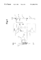
- FIG. 1 is a diagram showing a V/R circuit in accordance with a first embodiment of the present invention.
- a reference voltage circuit 10 , bleeder resistors 11 and 12 , an error amplifier circuit 13 and an output transistor 14 are identical with those used in the conventional V/R circuit.
- a clamp circuit 120 is added to the output of the error amplifier 13 .
- the clamp circuit 120 is made up of a constant-current circuit 121 , a capacitor 122 , a switch 123 and a Zener diode 124 .
- the operation of charging the capacitor 122 starts with a current from the constant-current circuit 121 , and the switch 123 is kept on until the capacitor 122 is charged to a given voltage.
- the output voltage Verr of the error amplifier 13 is clamped at VDD ⁇ Vz (clamp voltage) even if it is willing to be lower than a supply voltage VDD—the Zener voltage Vz, while the switch 123 is on.
- FIG. 3 The current to a power supply at the time of starting the V/R in case of the conventional V/R and the present invention are shown in FIG. 3.
- a broken line a indicates the current to the power supply in the conventional V/R whereas a solid line b indicates the current to the power supply in the V/R of the present invention.
- an axis of abscissa represents a time whereas an axis of ordinate represents a current to the power supply.
- the Zener diode is used as means for clamping the output of the error amplifier.
- FIG. 4 is a diagram showing a V/R circuit in accordance with a second embodiment of the present invention.
- a reference voltage circuit 10 , bleeder resistors 11 and 12 , an error amplifier 13 and an output transistor 14 are identical with those of the conventional V/R circuit described above.
- a difference from the first embodiment resides in that the clamp voltage of the clamp circuit in the error amplifier 13 varies in an analog manner as a time elapses.
- a clamp circuit 130 of the error amplifier 13 is made up of a constant-current circuit 131 , a capacitor 132 and a voltage follower circuit 133 .
- the capacitor 132 is charged by the constant-current circuit 131 at the time of starting the V/R so that a voltage Vp at a plus terminal of the voltage follower circuit 133 drops gradually from the supply voltage VDD. Assuming that the output of the voltage follower circuit 133 has no sinking capability but only source-operating capability, the output voltage Verr of the error amplifier 13 drops gradually from the supply voltage VDD while being clamped by the output of the voltage follower circuit 133 at the time of starting the V/R.
- FIG. 5 shows waveforms of the respective portions at the time of starting the V/R in accordance with the second embodiment of the present invention.
- An axis of abscissa represents a time whereas an axis of ordinate represents voltages at the respective portions.
- the output of the voltage follower circuit 133 drops from VDD together with a voltage Vp of its plus terminal. During this, since the output voltage Verr of the error amplifier 13 is clamped by the voltage follower circuit 133 , the on-resistance value of the output transistor of the V/R is suppressed to a certain value. In the meantime, when the voltage of Vp drops lower than the natural output voltage of the error amplifier, since the output of the voltage follower circuit 133 has no sinking capability, the same operation as that in the case where there is provided no clamp circuit is made.
- the output of the error amplifier is clamped at the time of starting the V/R, the same effect is obtained even in the case where, when there is a chip enable terminal (chip on/off terminal), the output of the error amplifier is clamped by its control signal without the limit of a case where the power supply turns on.
- the V/R control circuit and V/R of the present invention has an advantage in that the current to the power supply at the time of starting the V/R can be suppressed by clamping the output of the error amplifier at the time of starting the V/R.
Abstract
Description
Claims (31)
Applications Claiming Priority (2)
| Application Number | Priority Date | Filing Date | Title |
|---|---|---|---|
| JP10023681A JPH11224131A (en) | 1998-02-04 | 1998-02-04 | Voltage regulator |
| JP10-023681 | 1998-02-04 |
Publications (1)
| Publication Number | Publication Date |
|---|---|
| US6208123B1 true US6208123B1 (en) | 2001-03-27 |
Family
ID=12117215
Family Applications (1)
| Application Number | Title | Priority Date | Filing Date |
|---|---|---|---|
| US09/237,231 Expired - Lifetime US6208123B1 (en) | 1998-02-04 | 1999-01-26 | Voltage regulator with clamp circuit |
Country Status (4)
| Country | Link |
|---|---|
| US (1) | US6208123B1 (en) |
| JP (1) | JPH11224131A (en) |
| KR (2) | KR19990072377A (en) |
| TW (1) | TW421735B (en) |
Cited By (18)
| Publication number | Priority date | Publication date | Assignee | Title |
|---|---|---|---|---|
| US6452766B1 (en) * | 2000-10-30 | 2002-09-17 | National Semiconductor Corporation | Over-current protection circuit |
| US20040183587A1 (en) * | 2002-12-12 | 2004-09-23 | Matsushita Electric Industrial Co., Ltd. | Voltage generating circuit |
| US20040257053A1 (en) * | 2003-06-23 | 2004-12-23 | Rohm Co., Ltd. | Power supply circuit |
| US20040263137A1 (en) * | 2003-06-25 | 2004-12-30 | Rohm Co., Ltd. | Power supply circuit |
| US20070257644A1 (en) * | 2006-05-05 | 2007-11-08 | Standard Microsystems Corporation | Voltage regulator with inherent voltage clamping |
| US20090039853A1 (en) * | 2007-08-06 | 2009-02-12 | Rohm Co., Ltd. | Power supply device and electronic appliance provided therewith |
| US20100089670A1 (en) * | 2008-10-15 | 2010-04-15 | Hyundai Motor Company | Inverter circuit for vehicles |
| CN101025637B (en) * | 2006-02-20 | 2010-06-23 | 智原科技股份有限公司 | Current mode trimming device |
| US20100320993A1 (en) * | 2007-12-14 | 2010-12-23 | Ricoh Company, Ltd. | Constant voltage circuit |
| US8129959B1 (en) * | 2008-04-22 | 2012-03-06 | Fairchild Semiconductor Corporation | Start-up circuitry and method for power converter |
| US20120242316A1 (en) * | 2011-03-24 | 2012-09-27 | Minoru Sudo | Voltage regulator |
| US8558530B2 (en) | 2010-05-26 | 2013-10-15 | Smsc Holdings S.A.R.L. | Low power regulator |
| US20140104887A1 (en) * | 2012-10-12 | 2014-04-17 | Power Integrations, Inc. | Programming of an integrated circuit on a multi-function terminal |
| EP2735933A1 (en) * | 2012-11-26 | 2014-05-28 | Nxp B.V. | Startup control circuit in voltage regulators and related circuits |
| US20150137781A1 (en) * | 2012-09-05 | 2015-05-21 | Silicon Works Co., Ltd. | Low dropout circuit capable of controlled startup and method of controlling same |
| US20170017250A1 (en) * | 2015-07-15 | 2017-01-19 | Qualcomm Incorporated | Wide voltage range low drop-out regulators |
| CN109960306A (en) * | 2019-04-19 | 2019-07-02 | 海光信息技术有限公司 | Low pressure difference linear voltage regulator |
| WO2023173595A1 (en) * | 2022-03-14 | 2023-09-21 | 长鑫存储技术有限公司 | Voltage regulator and control method therefor |
Families Citing this family (10)
| Publication number | Priority date | Publication date | Assignee | Title |
|---|---|---|---|---|
| JP4559643B2 (en) * | 2000-02-29 | 2010-10-13 | セイコーインスツル株式会社 | Voltage regulator, switching regulator, and charge pump circuit |
| JP4732617B2 (en) * | 2001-06-08 | 2011-07-27 | セイコーインスツル株式会社 | Voltage regulator |
| JP4574902B2 (en) * | 2001-07-13 | 2010-11-04 | セイコーインスツル株式会社 | Voltage regulator |
| JP2005322105A (en) * | 2004-05-11 | 2005-11-17 | Seiko Instruments Inc | Constant voltage output circuit |
| KR100967028B1 (en) | 2008-06-03 | 2010-06-30 | 삼성전기주식회사 | Regulator with soft start using current source |
| KR101857084B1 (en) | 2011-06-30 | 2018-05-11 | 삼성전자주식회사 | Power supply module, electronic device including the same and method of the same |
| CN103809637B (en) * | 2012-11-13 | 2016-06-08 | 上海华虹宏力半导体制造有限公司 | Voltage-regulating circuit |
| KR101432494B1 (en) * | 2013-05-27 | 2014-08-21 | 주식회사엘디티 | Low drop out voltage regulator |
| CN107834847B (en) * | 2016-08-31 | 2020-03-31 | 杰华特微电子(张家港)有限公司 | Control circuit and control method of switching circuit and switching power supply circuit |
| CN111293881A (en) * | 2020-02-11 | 2020-06-16 | 中国安全生产科学研究院 | Control circuit |
Citations (5)
| Publication number | Priority date | Publication date | Assignee | Title |
|---|---|---|---|---|
| US4929883A (en) * | 1988-09-15 | 1990-05-29 | SGS-Thomson Mircroelectronics S.r.l. | Circuit for sensing the transistor current waveform |
| US4952863A (en) * | 1989-12-20 | 1990-08-28 | International Business Machines Corporation | Voltage regulator with power boost system |
| US5381082A (en) * | 1991-09-25 | 1995-01-10 | National Semiconductor Corporation | High-speed, fully-isolated current source/sink |
| US5686820A (en) * | 1995-06-15 | 1997-11-11 | International Business Machines Corporation | Voltage regulator with a minimal input voltage requirement |
| US5920182A (en) * | 1997-08-21 | 1999-07-06 | Stmicroelectronics S.A. | "Reset" type power supply voltage monitoring device |
Family Cites Families (4)
| Publication number | Priority date | Publication date | Assignee | Title |
|---|---|---|---|---|
| JPS57114917A (en) * | 1981-01-07 | 1982-07-17 | Mitsubishi Electric Corp | Constant voltage power supply circuit |
| JPH0552912A (en) * | 1991-08-27 | 1993-03-02 | Nec Corp | Integrated circuit |
| JPH05127764A (en) * | 1991-10-31 | 1993-05-25 | Nec Ic Microcomput Syst Ltd | Voltage regulator |
| JPH0552912U (en) * | 1991-12-05 | 1993-07-13 | セイコー電子工業株式会社 | Voltage regulator |
-
1998
- 1998-02-04 JP JP10023681A patent/JPH11224131A/en active Pending
-
1999
- 1999-01-26 US US09/237,231 patent/US6208123B1/en not_active Expired - Lifetime
- 1999-01-27 TW TW088101250A patent/TW421735B/en not_active IP Right Cessation
- 1999-02-02 KR KR1019990003394A patent/KR19990072377A/en not_active Application Discontinuation
-
2006
- 2006-08-16 KR KR1020060077223A patent/KR100700406B1/en not_active IP Right Cessation
Patent Citations (5)
| Publication number | Priority date | Publication date | Assignee | Title |
|---|---|---|---|---|
| US4929883A (en) * | 1988-09-15 | 1990-05-29 | SGS-Thomson Mircroelectronics S.r.l. | Circuit for sensing the transistor current waveform |
| US4952863A (en) * | 1989-12-20 | 1990-08-28 | International Business Machines Corporation | Voltage regulator with power boost system |
| US5381082A (en) * | 1991-09-25 | 1995-01-10 | National Semiconductor Corporation | High-speed, fully-isolated current source/sink |
| US5686820A (en) * | 1995-06-15 | 1997-11-11 | International Business Machines Corporation | Voltage regulator with a minimal input voltage requirement |
| US5920182A (en) * | 1997-08-21 | 1999-07-06 | Stmicroelectronics S.A. | "Reset" type power supply voltage monitoring device |
Cited By (34)
| Publication number | Priority date | Publication date | Assignee | Title |
|---|---|---|---|---|
| US6452766B1 (en) * | 2000-10-30 | 2002-09-17 | National Semiconductor Corporation | Over-current protection circuit |
| US20040183587A1 (en) * | 2002-12-12 | 2004-09-23 | Matsushita Electric Industrial Co., Ltd. | Voltage generating circuit |
| US6914474B2 (en) | 2002-12-12 | 2005-07-05 | Matsushita Electric Industrial Co., Ltd. | Voltage boosting circuit without output clamping for regulation |
| US20050231265A1 (en) * | 2002-12-12 | 2005-10-20 | Matsushita Electric Industrial Co., Ltd. | Voltage generating circuit |
| US7113026B2 (en) | 2002-12-12 | 2006-09-26 | Matsushita Electric Industrial Co., Ltd. | Voltage generating circuit |
| US20040257053A1 (en) * | 2003-06-23 | 2004-12-23 | Rohm Co., Ltd. | Power supply circuit |
| US7221132B2 (en) * | 2003-06-23 | 2007-05-22 | Rohm Co. Ltd. | Power supply circuit |
| CN100461062C (en) * | 2003-06-25 | 2009-02-11 | 罗姆股份有限公司 | Power supply circuit |
| US20040263137A1 (en) * | 2003-06-25 | 2004-12-30 | Rohm Co., Ltd. | Power supply circuit |
| US7071663B2 (en) * | 2003-06-25 | 2006-07-04 | Rohm Co., Ltd. | Power supply circuit |
| US20060152202A1 (en) * | 2003-06-25 | 2006-07-13 | Rohm Co., Ltd. | Power supply circuit |
| US7202647B2 (en) | 2003-06-25 | 2007-04-10 | Rohm Co., Ltd. | Power supply circuit |
| CN101025637B (en) * | 2006-02-20 | 2010-06-23 | 智原科技股份有限公司 | Current mode trimming device |
| US7602161B2 (en) | 2006-05-05 | 2009-10-13 | Standard Microsystems Corporation | Voltage regulator with inherent voltage clamping |
| US20070257644A1 (en) * | 2006-05-05 | 2007-11-08 | Standard Microsystems Corporation | Voltage regulator with inherent voltage clamping |
| US20090039853A1 (en) * | 2007-08-06 | 2009-02-12 | Rohm Co., Ltd. | Power supply device and electronic appliance provided therewith |
| US8169207B2 (en) * | 2007-08-06 | 2012-05-01 | Rohm Co., Ltd. | Power supply device including a clamping portion to limit and error voltage and electronic appliance provided therewith |
| US20100320993A1 (en) * | 2007-12-14 | 2010-12-23 | Ricoh Company, Ltd. | Constant voltage circuit |
| US8253404B2 (en) | 2007-12-14 | 2012-08-28 | Ricoh Company, Ltd. | Constant voltage circuit |
| US8129959B1 (en) * | 2008-04-22 | 2012-03-06 | Fairchild Semiconductor Corporation | Start-up circuitry and method for power converter |
| US20100089670A1 (en) * | 2008-10-15 | 2010-04-15 | Hyundai Motor Company | Inverter circuit for vehicles |
| US8410746B2 (en) | 2008-10-15 | 2013-04-02 | Hyundai Motor Company | Inverter circuit for vehicles |
| US8558530B2 (en) | 2010-05-26 | 2013-10-15 | Smsc Holdings S.A.R.L. | Low power regulator |
| US8547080B2 (en) * | 2011-03-24 | 2013-10-01 | Seiko Instruments Inc. | Voltage regulator |
| US20120242316A1 (en) * | 2011-03-24 | 2012-09-27 | Minoru Sudo | Voltage regulator |
| US20150137781A1 (en) * | 2012-09-05 | 2015-05-21 | Silicon Works Co., Ltd. | Low dropout circuit capable of controlled startup and method of controlling same |
| US20140104887A1 (en) * | 2012-10-12 | 2014-04-17 | Power Integrations, Inc. | Programming of an integrated circuit on a multi-function terminal |
| US9036369B2 (en) * | 2012-10-12 | 2015-05-19 | Power Integrations, Inc. | Programming of an integrated circuit on a multi-function terminal |
| EP2735933A1 (en) * | 2012-11-26 | 2014-05-28 | Nxp B.V. | Startup control circuit in voltage regulators and related circuits |
| US20170017250A1 (en) * | 2015-07-15 | 2017-01-19 | Qualcomm Incorporated | Wide voltage range low drop-out regulators |
| US9817415B2 (en) * | 2015-07-15 | 2017-11-14 | Qualcomm Incorporated | Wide voltage range low drop-out regulators |
| CN109960306A (en) * | 2019-04-19 | 2019-07-02 | 海光信息技术有限公司 | Low pressure difference linear voltage regulator |
| CN109960306B (en) * | 2019-04-19 | 2020-08-18 | 海光信息技术有限公司 | Low dropout linear regulator |
| WO2023173595A1 (en) * | 2022-03-14 | 2023-09-21 | 长鑫存储技术有限公司 | Voltage regulator and control method therefor |
Also Published As
| Publication number | Publication date |
|---|---|
| KR20060096398A (en) | 2006-09-11 |
| JPH11224131A (en) | 1999-08-17 |
| KR100700406B1 (en) | 2007-03-28 |
| TW421735B (en) | 2001-02-11 |
| KR19990072377A (en) | 1999-09-27 |
Similar Documents
| Publication | Publication Date | Title |
|---|---|---|
| US6208123B1 (en) | Voltage regulator with clamp circuit | |
| US4779037A (en) | Dual input low dropout voltage regulator | |
| US4823070A (en) | Switching voltage regulator circuit | |
| US5861771A (en) | Regulator circuit and semiconductor integrated circuit device having the same | |
| EP0864956A2 (en) | Low dropout regulators | |
| US20070018623A1 (en) | Low-dropout regulator with startup overshoot control | |
| US6559623B1 (en) | In-rush current control for a low drop-out voltage regulator | |
| US20040245974A1 (en) | Switching regulator | |
| US9606556B2 (en) | Semiconductor integrated circuit for regulator | |
| EP2701030A1 (en) | Low dropout voltage regulator with a floating voltage reference | |
| US8129962B2 (en) | Low dropout voltage regulator with clamping | |
| JP2012088987A (en) | Semiconductor integrated circuit for regulators | |
| GB2267003A (en) | Current-limiting cicuit and constant voltage source therefor; current regulator | |
| JP7354380B2 (en) | Electrical circuits that allow electronic components to start and shut down safely | |
| US6232753B1 (en) | Voltage regulator for driving plural loads based on the number of loads being driven | |
| US5945819A (en) | Voltage regulator with fast response | |
| US11874680B2 (en) | Power supply with integrated voltage regulator and current limiter and method | |
| US4574232A (en) | Rapid turn-on voltage regulator | |
| US7042280B1 (en) | Over-current protection circuit | |
| EP3703234B1 (en) | Switching regulator with proportional-integral (pi) control compensation network clamp | |
| WO2022125514A1 (en) | Supply-glitch-tolerant regulator | |
| US5122945A (en) | Voltage controlled preload | |
| US6683442B1 (en) | Soft start of a switching power supply system | |
| US5977755A (en) | Constant-voltage power supply circuit | |
| US6486646B2 (en) | Apparatus for generating constant reference voltage signal regardless of temperature change |
Legal Events
| Date | Code | Title | Description |
|---|---|---|---|
| AS | Assignment |
Owner name: SEIKO INSTRUMENTS, INC, JAPAN Free format text: ASSIGNMENT OF ASSIGNORS INTEREST;ASSIGNOR:SUDO, MINORU;REEL/FRAME:011472/0855 Effective date: 20001208 |
|
| STCF | Information on status: patent grant |
Free format text: PATENTED CASE |
|
| FPAY | Fee payment |
Year of fee payment: 4 |
|
| FPAY | Fee payment |
Year of fee payment: 8 |
|
| FPAY | Fee payment |
Year of fee payment: 12 |
|
| AS | Assignment |
Owner name: SII SEMICONDUCTOR CORPORATION, JAPAN Free format text: ASSIGNMENT OF ASSIGNORS INTEREST;ASSIGNOR:SEIKO INSTRUMENTS INC.;REEL/FRAME:038058/0892 Effective date: 20160105 |
|
| AS | Assignment |
Owner name: ABLIC INC., JAPAN Free format text: CHANGE OF NAME;ASSIGNOR:SII SEMICONDUCTOR CORPORATION;REEL/FRAME:045567/0927 Effective date: 20180105 |