US6214685B1 - Phosphate coating for varistor and method - Google Patents
Phosphate coating for varistor and method Download PDFInfo
- Publication number
- US6214685B1 US6214685B1 US09/108,961 US10896198A US6214685B1 US 6214685 B1 US6214685 B1 US 6214685B1 US 10896198 A US10896198 A US 10896198A US 6214685 B1 US6214685 B1 US 6214685B1
- Authority
- US
- United States
- Prior art keywords
- oxide
- phosphate
- phosphoric acid
- acid solution
- saturating
- Prior art date
- Legal status (The legal status is an assumption and is not a legal conclusion. Google has not performed a legal analysis and makes no representation as to the accuracy of the status listed.)
- Expired - Fee Related
Links
Images
Classifications
-
- H—ELECTRICITY
- H01—ELECTRIC ELEMENTS
- H01C—RESISTORS
- H01C1/00—Details
- H01C1/14—Terminals or tapping points or electrodes specially adapted for resistors; Arrangements of terminals or tapping points or electrodes on resistors
- H01C1/142—Terminals or tapping points or electrodes specially adapted for resistors; Arrangements of terminals or tapping points or electrodes on resistors the terminals or tapping points being coated on the resistive element
-
- H—ELECTRICITY
- H01—ELECTRIC ELEMENTS
- H01C—RESISTORS
- H01C1/00—Details
- H01C1/02—Housing; Enclosing; Embedding; Filling the housing or enclosure
- H01C1/034—Housing; Enclosing; Embedding; Filling the housing or enclosure the housing or enclosure being formed as coating or mould without outer sheath
-
- H—ELECTRICITY
- H01—ELECTRIC ELEMENTS
- H01C—RESISTORS
- H01C7/00—Non-adjustable resistors formed as one or more layers or coatings; Non-adjustable resistors made from powdered conducting material or powdered semi-conducting material with or without insulating material
- H01C7/10—Non-adjustable resistors formed as one or more layers or coatings; Non-adjustable resistors made from powdered conducting material or powdered semi-conducting material with or without insulating material voltage responsive, i.e. varistors
- H01C7/102—Varistor boundary, e.g. surface layers
-
- H—ELECTRICITY
- H01—ELECTRIC ELEMENTS
- H01C—RESISTORS
- H01C7/00—Non-adjustable resistors formed as one or more layers or coatings; Non-adjustable resistors made from powdered conducting material or powdered semi-conducting material with or without insulating material
- H01C7/18—Non-adjustable resistors formed as one or more layers or coatings; Non-adjustable resistors made from powdered conducting material or powdered semi-conducting material with or without insulating material comprising a plurality of layers stacked between terminals
-
- Y—GENERAL TAGGING OF NEW TECHNOLOGICAL DEVELOPMENTS; GENERAL TAGGING OF CROSS-SECTIONAL TECHNOLOGIES SPANNING OVER SEVERAL SECTIONS OF THE IPC; TECHNICAL SUBJECTS COVERED BY FORMER USPC CROSS-REFERENCE ART COLLECTIONS [XRACs] AND DIGESTS
- Y10—TECHNICAL SUBJECTS COVERED BY FORMER USPC
- Y10S—TECHNICAL SUBJECTS COVERED BY FORMER USPC CROSS-REFERENCE ART COLLECTIONS [XRACs] AND DIGESTS
- Y10S438/00—Semiconductor device manufacturing: process
- Y10S438/957—Making metal-insulator-metal device
Definitions
- the present invention relates to nonlinear resistive devices, such as varistors, and more particularly to methods of making such devices using various plating techniques in which only the electrically contactable end terminals of the device are plated.
- Nonlinear resistive devices are known in the art, and are described, for example, in U.S. Pat. No. 5,115,221 issued to Cowman on May 19, 1992, that is incorporated by reference.
- a typical device 10 may include plural layers 12 of semiconductor material with electrically conductive electrodes 14 between adjacent layers. A portion of each electrode 14 is exposed in a terminal region 16 so that electrical contact may be made therewith. The electrodes 14 may be exposed at one or both of opposing terminal regions, and typically the electrodes are exposed at alternating terminal regions 16 as illustrated. The exposed portions of the electrodes 14 are contacted by electrically conductive end terminals 18 that cover the terminal regions 16 .
- the manufacture of such devices has proved complex.
- the attachment of the end terminals 18 has proved to be a difficult problem in search of a simplified solution.
- the terminal regions 16 may be plated with nickel and tin-lead metals to increase solderability and decrease solder leaching.
- the process parameters in plating nickel to zinc oxide semiconductor bodies has proved particularly vexing and has required complex solutions.
- One method of affixing the end terminals 18 is to use a conventional barrel plating method in which the entire device is immersed in a plating solution.
- the stacked layers are semiconductor material, such as zinc oxide, that may be conductive during the plating process so that the plating adheres to the entire surface of the device.
- a portion of the plating must be mechanically removed after immersion, or covered before immersion with a temporary plating resist comprised of an organic substance insoluble to the plating solution.
- the removal of the plating or organic plating resist is an extra step in the manufacturing process, and may involve the use of toxic materials that further complicate the manufacturing process.
- the metal forming the end terminals 18 be flame sprayed onto the device, with the other portions of the surface of the device being masked. Flame spraying is not suitable for many manufacturing processes because it is slow and includes the creation of a special mask, with the additional steps attendant therewith. See, for example, U.S. Pat. No. 4,316,171 issued to Miyabayashi, et al. on Feb. 16, 1982.
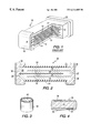
- FIG. 1 is a pictorial depiction of a varistor typical of the prior art.
- FIG. 2 is vertical cross section of an embodiment of the device of the present invention.
- FIG. 3 is a pictorial depiction of a high energy disc varistor with an insulating layer of the present invention thereon.
- FIG. 4 is a pictorial depiction of a surface mount device with an insulating layer of the present invention.
- an embodiment of a nonlinear resistive element 20 may include a body 22 having stacked semiconductor layers 24 with generally planar electrodes 26 between adjacent pairs of the semiconductor layers 24 .
- the semiconductor layers 24 comprise a metal oxide such as zinc oxide or iron oxide and need not be comprised of pure metal oxide as layers 24 may be comprised of a ceramic consisting principally of metal oxide.
- Each electrode 26 may have a contactable portion 28 that is exposed for electrical connection to the electrically conductive metal (preferably silver, silver-platinum, or silver-palladium) end terminations 30 that cover the terminal regions 32 of the body 22 and contact the electrodes 26 .
- the portions of the body 22 not covered with the end terminations 30 are coated with an electrically insulative zinc phosphate layer 34 .
- the end terminations 30 may be plated with layers 36 of electrically conductive metal that form electrically contactable end portions for the resistive element 20 .
- the zinc oxide semiconductor layers 24 may have the following composition in mole percent: 94-98% zinc oxide and 2-6% of one or more of the following additives; bismuth oxide, cobalt oxide, manganese oxide, nickel oxide, antimony oxide, boric oxide, chromium oxide, silicon oxide, aluminum nitrate, and other equivalents.
- the device body 22 and the end terminations 30 may be provided conventionally.
- the deposited phosphate layer 34 may be formed on the device body 22 by a passivation process by reacting a phosphoric acid solution with the metal oxide semiconductor layers 24 exposed at the exterior of the body 22 .
- the device body 22 is saturated in the phosphoric acid solution to thereby form the phosphate layer 34 by deposition of phosphate in the acid solution onto the exposed semiconductor layers 24 .
- the phosphoric acid solution may comprise phosphoric acid, zinc oxide or a zinc salt, and a pH modifier such as ammonia.
- Zinc phosphate forms in the solution and deposits onto the exposed surface of the zinc oxide semiconductor layer 24 during the passivation process.
- the phosphoric acid solution desirably has a pH of 2 to 4 but the pH of solution may be 1 to 5.
- the reaction may take place for 10 to 50 minutes at an operating temperature of 15° C. to 70° C.
- the time required for the reaction is dependent on the thickness of the layer required for the specific temperature and pH conditions of the reaction.
- the operating conditions of the reaction may also be modified within the specified ranges to accommodate different semiconducting device designs.
- one part phosphoric acid may be added to one hundred parts deionized water.
- the pH of the solution is modified to 2 and the solution is heated to a temperature above 30° C.
- the body 22 with end terminations 30 affixed may be washed with acetone and dried at about 100° C. for ten minutes.
- the washed device may be submerged in the phosphoric acid solution for thirty minutes to provide the layer 34 .
- the body may be cleaned with deionized water and dried at about 100° C. for about fifteen minutes.
- the layer 34 does not adhere to the end terminations 30 because the silver or silver-platinum in the end terminations 30 is not affected by the phosphoric acid.
- the phosphoric acid solution may also be applied by spraying, instead of submerging, the device.
- the device may be plated with an electrically conductive metal, such as nickel and tin-lead, to provide the layers 36 .
- an electrically conductive metal such as nickel and tin-lead
- a conventional barrel plating process may be used, although the pH of the plating solution is desirably kept between about 4.0 and 6.0. In the barrel plating process the device is made electrically conductive and the plating material adheres to the electrically charged portions of the device.
- the metal plating of layers 36 does not plate the zinc phosphate layer 34 during the barrel plating because the zinc phosphate is not electrically conductive.
- the zinc phosphate layer 34 is electrically insulating and may be retained in the final product to provide additional protection.
- the layer 34 does not effect the I-V characteristics of the device.
- the phosphate layer may be an inorganic oxide layer formed by the reaction of phosphoric acid with the metal oxide semiconductor in the device.
- the semiconductor may be iron oxide, a ferrite, etc.
- a high energy disc varistor has a glass or polymer insulating layer on its sides.
- the disc varistor 40 may have an insulating layer 42 of phosphate formed in the manner discussed above.
- the present invention is applicable to other varistor products such as a surface mount device depicted in FIG. 4, radial parts, arrays, connector pins, discoidal construction, etc.
Abstract
Description
Claims (15)
Priority Applications (3)
| Application Number | Priority Date | Filing Date | Title |
|---|---|---|---|
| US09/108,961 US6214685B1 (en) | 1998-07-02 | 1998-07-02 | Phosphate coating for varistor and method |
| EP99111349A EP0969481A1 (en) | 1998-07-02 | 1999-06-10 | Phosphate coating for varistor and method |
| JP11177824A JP2000030911A (en) | 1998-07-02 | 1999-06-24 | Phosphate coating film for varistor and its method |
Applications Claiming Priority (1)
| Application Number | Priority Date | Filing Date | Title |
|---|---|---|---|
| US09/108,961 US6214685B1 (en) | 1998-07-02 | 1998-07-02 | Phosphate coating for varistor and method |
Publications (1)
| Publication Number | Publication Date |
|---|---|
| US6214685B1 true US6214685B1 (en) | 2001-04-10 |
Family
ID=22325064
Family Applications (1)
| Application Number | Title | Priority Date | Filing Date |
|---|---|---|---|
| US09/108,961 Expired - Fee Related US6214685B1 (en) | 1998-07-02 | 1998-07-02 | Phosphate coating for varistor and method |
Country Status (3)
| Country | Link |
|---|---|
| US (1) | US6214685B1 (en) |
| EP (1) | EP0969481A1 (en) |
| JP (1) | JP2000030911A (en) |
Cited By (21)
| Publication number | Priority date | Publication date | Assignee | Title |
|---|---|---|---|---|
| US20030150741A1 (en) * | 2002-02-08 | 2003-08-14 | Thinking Electronic Industrial Co., Ltd. | Varistor and fabricating method of zinc phosphate insulation for the same |
| US20030231457A1 (en) * | 2002-04-15 | 2003-12-18 | Avx Corporation | Plated terminations |
| US20040197973A1 (en) * | 2002-04-15 | 2004-10-07 | Ritter Andrew P. | Component formation via plating technology |
| US20040218344A1 (en) * | 2002-04-15 | 2004-11-04 | Ritter Andrew P. | Plated terminations |
| US20040257748A1 (en) * | 2002-04-15 | 2004-12-23 | Avx Corporation | Plated terminations |
| US6960366B2 (en) | 2002-04-15 | 2005-11-01 | Avx Corporation | Plated terminations |
| US20070128822A1 (en) * | 2005-10-19 | 2007-06-07 | Littlefuse, Inc. | Varistor and production method |
| US20070133147A1 (en) * | 2002-04-15 | 2007-06-14 | Avx Corporation | System and method of plating ball grid array and isolation features for electronic components |
| US7576968B2 (en) | 2002-04-15 | 2009-08-18 | Avx Corporation | Plated terminations and method of forming using electrolytic plating |
| US20090251841A1 (en) * | 2008-04-04 | 2009-10-08 | Littelfuse, Inc. | Incorporating electrostatic protection into miniature connectors |
| US20100044698A1 (en) * | 2005-10-12 | 2010-02-25 | Gregory Herman | Semiconductor Film Composition |
| US20100071949A1 (en) * | 2008-03-28 | 2010-03-25 | Tdk Corporation | Electronic component |
| US20100189882A1 (en) * | 2006-09-19 | 2010-07-29 | Littelfuse Ireland Development Company Limited | Manufacture of varistors with a passivation layer |
| CN104969307A (en) * | 2013-01-29 | 2015-10-07 | 株式会社村田制作所 | Ceramic electronic component and manufacturing method therefor |
| US20150380151A1 (en) * | 2014-06-25 | 2015-12-31 | Samsung Electro-Mechanics Co., Ltd. | Chip coil component and method of manufacturing the same |
| US20160027561A1 (en) * | 2014-07-28 | 2016-01-28 | Murata Manufacturing Co., Ltd. | Ceramic electronic component |
| CN105304239A (en) * | 2014-07-28 | 2016-02-03 | 株式会社村田制作所 | Ceramic electronic component and manufacturing method therefor |
| US20160276089A1 (en) * | 2015-03-19 | 2016-09-22 | Murata Manufacturing Co., Ltd. | Electronic component and method for manufacturing electronic component |
| US20180286559A1 (en) * | 2017-03-29 | 2018-10-04 | Samsung Electro-Mechanics Co., Ltd. | Electronic component and system-in-package |
| US11037710B2 (en) | 2018-07-18 | 2021-06-15 | Avx Corporation | Varistor passivation layer and method of making the same |
| US11081283B2 (en) * | 2019-06-03 | 2021-08-03 | Samsung Electro-Mechanics Co., Ltd. | Multi-layered ceramic electronic component and mounting board thereof |
Families Citing this family (2)
| Publication number | Priority date | Publication date | Assignee | Title |
|---|---|---|---|---|
| CN101717978B (en) * | 2009-12-16 | 2014-10-01 | 深圳顺络电子股份有限公司 | Preliminary treatment method for electroplating of chip ferrite product |
| KR20220146543A (en) * | 2020-02-27 | 2022-11-01 | 본스인코오포레이티드 | MOV-related devices and methods with modified edges |
Citations (4)
| Publication number | Priority date | Publication date | Assignee | Title |
|---|---|---|---|---|
| US3784417A (en) * | 1971-10-26 | 1974-01-08 | Dow Chemical Co | Surface conversion treatment for magnesium alloys |
| US4140551A (en) * | 1977-08-19 | 1979-02-20 | Heatbath Corporation | Low temperature microcrystalline zinc phosphate coatings, compositions, and processes for using and preparing the same |
| US5757263A (en) * | 1994-12-09 | 1998-05-26 | Harris Corporation | Zinc phosphate coating for varistor |
| US5858518A (en) * | 1996-02-13 | 1999-01-12 | Nitto Denko Corporation | Circuit substrate, circuit-formed suspension substrate, and production method thereof |
Family Cites Families (2)
| Publication number | Priority date | Publication date | Assignee | Title |
|---|---|---|---|---|
| CA1186130A (en) * | 1981-06-16 | 1985-04-30 | Jeffery L. Barrall | Rigid, water-resistant phosphate ceramic materials and processes for preparing them |
| EP0806780B1 (en) * | 1996-05-09 | 2000-08-02 | Littlefuse, Inc. | Zinc phosphate coating for varistor and method |
-
1998
- 1998-07-02 US US09/108,961 patent/US6214685B1/en not_active Expired - Fee Related
-
1999
- 1999-06-10 EP EP99111349A patent/EP0969481A1/en not_active Withdrawn
- 1999-06-24 JP JP11177824A patent/JP2000030911A/en active Pending
Patent Citations (4)
| Publication number | Priority date | Publication date | Assignee | Title |
|---|---|---|---|---|
| US3784417A (en) * | 1971-10-26 | 1974-01-08 | Dow Chemical Co | Surface conversion treatment for magnesium alloys |
| US4140551A (en) * | 1977-08-19 | 1979-02-20 | Heatbath Corporation | Low temperature microcrystalline zinc phosphate coatings, compositions, and processes for using and preparing the same |
| US5757263A (en) * | 1994-12-09 | 1998-05-26 | Harris Corporation | Zinc phosphate coating for varistor |
| US5858518A (en) * | 1996-02-13 | 1999-01-12 | Nitto Denko Corporation | Circuit substrate, circuit-formed suspension substrate, and production method thereof |
Non-Patent Citations (1)
| Title |
|---|
| Petrucci, "General Chemistry Principles and Modern Applications" 5th edition; p. 620 1989. * |
Cited By (54)
| Publication number | Priority date | Publication date | Assignee | Title |
|---|---|---|---|---|
| US6841191B2 (en) * | 2002-02-08 | 2005-01-11 | Thinking Electronic Industrial Co., Ltd. | Varistor and fabricating method of zinc phosphate insulation for the same |
| US20030150741A1 (en) * | 2002-02-08 | 2003-08-14 | Thinking Electronic Industrial Co., Ltd. | Varistor and fabricating method of zinc phosphate insulation for the same |
| US7154374B2 (en) | 2002-04-15 | 2006-12-26 | Avx Corporation | Plated terminations |
| US20030231457A1 (en) * | 2002-04-15 | 2003-12-18 | Avx Corporation | Plated terminations |
| US20040218344A1 (en) * | 2002-04-15 | 2004-11-04 | Ritter Andrew P. | Plated terminations |
| US20040257748A1 (en) * | 2002-04-15 | 2004-12-23 | Avx Corporation | Plated terminations |
| US20040264105A1 (en) * | 2002-04-15 | 2004-12-30 | Galvagni John L. | Component formation via plating technology |
| US20040197973A1 (en) * | 2002-04-15 | 2004-10-07 | Ritter Andrew P. | Component formation via plating technology |
| US20050046536A1 (en) * | 2002-04-15 | 2005-03-03 | Ritter Andrew P. | Plated terminations |
| US20050146837A1 (en) * | 2002-04-15 | 2005-07-07 | Ritter Andrew P. | Plated terminations |
| US6960366B2 (en) | 2002-04-15 | 2005-11-01 | Avx Corporation | Plated terminations |
| US6972942B2 (en) | 2002-04-15 | 2005-12-06 | Avx Corporation | Plated terminations |
| US6982863B2 (en) | 2002-04-15 | 2006-01-03 | Avx Corporation | Component formation via plating technology |
| US7067172B2 (en) | 2002-04-15 | 2006-06-27 | Avx Corporation | Component formation via plating technology |
| US9666366B2 (en) | 2002-04-15 | 2017-05-30 | Avx Corporation | Method of making multi-layer electronic components with plated terminations |
| US20040218373A1 (en) * | 2002-04-15 | 2004-11-04 | Ritter Andrew P. | Plated terminations |
| US7344981B2 (en) | 2002-04-15 | 2008-03-18 | Avx Corporation | Plated terminations |
| US7177137B2 (en) | 2002-04-15 | 2007-02-13 | Avx Corporation | Plated terminations |
| US7152291B2 (en) | 2002-04-15 | 2006-12-26 | Avx Corporation | Method for forming plated terminations |
| US20070133147A1 (en) * | 2002-04-15 | 2007-06-14 | Avx Corporation | System and method of plating ball grid array and isolation features for electronic components |
| US7161794B2 (en) | 2002-04-15 | 2007-01-09 | Avx Corporation | Component formation via plating technology |
| US7463474B2 (en) | 2002-04-15 | 2008-12-09 | Avx Corporation | System and method of plating ball grid array and isolation features for electronic components |
| US7576968B2 (en) | 2002-04-15 | 2009-08-18 | Avx Corporation | Plated terminations and method of forming using electrolytic plating |
| US11195659B2 (en) | 2002-04-15 | 2021-12-07 | Avx Corporation | Plated terminations |
| US10366835B2 (en) | 2002-04-15 | 2019-07-30 | Avx Corporation | Plated terminations |
| US10020116B2 (en) | 2002-04-15 | 2018-07-10 | Avx Corporation | Plated terminations |
| US20100044698A1 (en) * | 2005-10-12 | 2010-02-25 | Gregory Herman | Semiconductor Film Composition |
| US8969865B2 (en) * | 2005-10-12 | 2015-03-03 | Hewlett-Packard Development Company, L.P. | Semiconductor film composition |
| US20070128822A1 (en) * | 2005-10-19 | 2007-06-07 | Littlefuse, Inc. | Varistor and production method |
| EP2958120A1 (en) | 2006-08-10 | 2015-12-23 | AVX Corporation | Multilayer electronic component with electrolytically plated terminations |
| US20100189882A1 (en) * | 2006-09-19 | 2010-07-29 | Littelfuse Ireland Development Company Limited | Manufacture of varistors with a passivation layer |
| US8106506B2 (en) * | 2008-03-28 | 2012-01-31 | Tdk Corporation | Electronic component |
| US20100071949A1 (en) * | 2008-03-28 | 2010-03-25 | Tdk Corporation | Electronic component |
| US20090251841A1 (en) * | 2008-04-04 | 2009-10-08 | Littelfuse, Inc. | Incorporating electrostatic protection into miniature connectors |
| DE102009015962A1 (en) | 2008-04-04 | 2009-11-05 | Littlefuse, Inc., Des Plaines | Insertion of electrostatic protection in miniature connectors |
| US7952848B2 (en) | 2008-04-04 | 2011-05-31 | Littelfuse, Inc. | Incorporating electrostatic protection into miniature connectors |
| US9997293B2 (en) * | 2013-01-29 | 2018-06-12 | Murata Manufacturing Co., Ltd. | Ceramic electronic component and manufacturing method therefor |
| US20150325369A1 (en) * | 2013-01-29 | 2015-11-12 | Murata Manufacturing Co., Ltd. | Ceramic electronic component and manufacturing method therefor |
| CN104969307A (en) * | 2013-01-29 | 2015-10-07 | 株式会社村田制作所 | Ceramic electronic component and manufacturing method therefor |
| CN104969307B (en) * | 2013-01-29 | 2018-09-28 | 株式会社村田制作所 | Ceramic electronic components and its manufacturing method |
| US20150380151A1 (en) * | 2014-06-25 | 2015-12-31 | Samsung Electro-Mechanics Co., Ltd. | Chip coil component and method of manufacturing the same |
| CN105304322A (en) * | 2014-07-28 | 2016-02-03 | 株式会社村田制作所 | Ceramic electronic component |
| US9959975B2 (en) * | 2014-07-28 | 2018-05-01 | Murata Manufacturing Co., Ltd. | Ceramic electronic component |
| CN105304322B (en) * | 2014-07-28 | 2019-03-01 | 株式会社村田制作所 | Ceramic electronic components |
| US10304630B2 (en) | 2014-07-28 | 2019-05-28 | Murata Manufacturing Co., Ltd. | Ceramic electronic component and manufacturing method therefor |
| CN105304239A (en) * | 2014-07-28 | 2016-02-03 | 株式会社村田制作所 | Ceramic electronic component and manufacturing method therefor |
| US20160027561A1 (en) * | 2014-07-28 | 2016-01-28 | Murata Manufacturing Co., Ltd. | Ceramic electronic component |
| US20160276089A1 (en) * | 2015-03-19 | 2016-09-22 | Murata Manufacturing Co., Ltd. | Electronic component and method for manufacturing electronic component |
| US10875095B2 (en) * | 2015-03-19 | 2020-12-29 | Murata Manufacturing Co., Ltd. | Electronic component comprising magnetic metal powder |
| US11817244B2 (en) | 2015-03-19 | 2023-11-14 | Murata Manufacturing Co., Ltd. | Method for manufacturing electronic component |
| US20180286559A1 (en) * | 2017-03-29 | 2018-10-04 | Samsung Electro-Mechanics Co., Ltd. | Electronic component and system-in-package |
| US10607764B2 (en) * | 2017-03-29 | 2020-03-31 | Samsung Electro-Mechanics Co., Ltd. | Electronic component and system-in-package |
| US11037710B2 (en) | 2018-07-18 | 2021-06-15 | Avx Corporation | Varistor passivation layer and method of making the same |
| US11081283B2 (en) * | 2019-06-03 | 2021-08-03 | Samsung Electro-Mechanics Co., Ltd. | Multi-layered ceramic electronic component and mounting board thereof |
Also Published As
| Publication number | Publication date |
|---|---|
| EP0969481A1 (en) | 2000-01-05 |
| JP2000030911A (en) | 2000-01-28 |
Similar Documents
| Publication | Publication Date | Title |
|---|---|---|
| US6214685B1 (en) | Phosphate coating for varistor and method | |
| US5614074A (en) | Zinc phosphate coating for varistor and method | |
| CN111886663B (en) | Multilayer ceramic capacitor with ultra-wideband performance | |
| US4613518A (en) | Monolithic capacitor edge termination | |
| CN113330527B (en) | Multilayer ceramic capacitor with ultra-wideband performance | |
| US6232144B1 (en) | Nickel barrier end termination and method | |
| US6841191B2 (en) | Varistor and fabricating method of zinc phosphate insulation for the same | |
| US4510179A (en) | Electrode on heat-resisting and isolating substrate and the manufacturing process for it | |
| EP0806780B1 (en) | Zinc phosphate coating for varistor and method | |
| US2793178A (en) | Method of providing insulator with multiplicity of conducting elements | |
| US6278065B1 (en) | Apparatus and method for minimizing currents in electrical devices | |
| EP0973176A1 (en) | Nickel barrier end termination and method | |
| US4559279A (en) | Electrode on heat-resisting and isolating substrate | |
| TWI760706B (en) | Electronic component packaging structure and manufacturing method thereof | |
| GB2384493A (en) | Selective electroless plating of ceramic substrates for use in capacitors | |
| JPS60117684A (en) | Manufacture of amorphous si solar battery | |
| JPH0397212A (en) | Chip type solid-state electrolytic capacitor | |
| JPS6311792B2 (en) | ||
| JPS634329B2 (en) | ||
| JPS59126399A (en) | Manufacture of electrode of ceramic electric component | |
| JPH0458188B2 (en) | ||
| JPS5835957A (en) | Manufacture of hybrid integrated circuit | |
| JPH06290918A (en) | Manufacture of chip resistor | |
| CN1241007A (en) | Nickel barrier end termination and method for forming same | |
| JPS631729B2 (en) |
Legal Events
| Date | Code | Title | Description |
|---|---|---|---|
| AS | Assignment |
Owner name: HARRIS CORPORATION, FLORIDA Free format text: ASSIGNMENT OF ASSIGNORS INTEREST;ASSIGNORS:CLINTON, CAROLINE;SPALDING, TREVOR R.;CONNELL, ANDREW MARK;AND OTHERS;REEL/FRAME:009705/0645;SIGNING DATES FROM 19981119 TO 19990113 |
|
| AS | Assignment |
Owner name: LITTELFUSE, INC., ILLINOIS Free format text: ASSIGNMENT OF ASSIGNORS INTEREST;ASSIGNOR:HARRIS CORPORATION; ECCO PARENT LTD.;REEL/FRAME:010766/0264 Effective date: 19991019 Owner name: LITTELFUSE, INC., ILLINOIS Free format text: ASSIGNMENT OF ASSIGNORS INTEREST;ASSIGNOR:HARRIS CORPORATION; HARRIS IRELAND, LTD.;REEL/FRAME:010766/0318 Effective date: 19991012 |
|
| AS | Assignment |
Owner name: LITTELFUSE, INC., ILLINOIS Free format text: ASSIGNMENT OF ASSIGNORS INTEREST;ASSIGNOR:HARRIS CORPORATION;REEL/FRAME:011432/0522 Effective date: 19991019 |
|
| FPAY | Fee payment |
Year of fee payment: 4 |
|
| FPAY | Fee payment |
Year of fee payment: 8 |
|
| REMI | Maintenance fee reminder mailed | ||
| LAPS | Lapse for failure to pay maintenance fees | ||
| STCH | Information on status: patent discontinuation |
Free format text: PATENT EXPIRED DUE TO NONPAYMENT OF MAINTENANCE FEES UNDER 37 CFR 1.362 |
|
| FP | Lapsed due to failure to pay maintenance fee |
Effective date: 20130410 |