US6223989B1 - Method for making smart cards, and resulting cards - Google Patents
Method for making smart cards, and resulting cards Download PDFInfo
- Publication number
- US6223989B1 US6223989B1 US09/230,850 US23085099A US6223989B1 US 6223989 B1 US6223989 B1 US 6223989B1 US 23085099 A US23085099 A US 23085099A US 6223989 B1 US6223989 B1 US 6223989B1
- Authority
- US
- United States
- Prior art keywords
- cavity
- module
- deposited
- gluing
- glue
- Prior art date
- Legal status (The legal status is an assumption and is not a legal conclusion. Google has not performed a legal analysis and makes no representation as to the accuracy of the status listed.)
- Expired - Lifetime
Links
Images


Classifications
-
- G—PHYSICS
- G06—COMPUTING; CALCULATING OR COUNTING
- G06K—GRAPHICAL DATA READING; PRESENTATION OF DATA; RECORD CARRIERS; HANDLING RECORD CARRIERS
- G06K19/00—Record carriers for use with machines and with at least a part designed to carry digital markings
- G06K19/06—Record carriers for use with machines and with at least a part designed to carry digital markings characterised by the kind of the digital marking, e.g. shape, nature, code
- G06K19/067—Record carriers with conductive marks, printed circuits or semiconductor circuit elements, e.g. credit or identity cards also with resonating or responding marks without active components
- G06K19/07—Record carriers with conductive marks, printed circuits or semiconductor circuit elements, e.g. credit or identity cards also with resonating or responding marks without active components with integrated circuit chips
- G06K19/077—Constructional details, e.g. mounting of circuits in the carrier
- G06K19/07743—External electrical contacts
-
- G—PHYSICS
- G06—COMPUTING; CALCULATING OR COUNTING
- G06K—GRAPHICAL DATA READING; PRESENTATION OF DATA; RECORD CARRIERS; HANDLING RECORD CARRIERS
- G06K19/00—Record carriers for use with machines and with at least a part designed to carry digital markings
- G06K19/06—Record carriers for use with machines and with at least a part designed to carry digital markings characterised by the kind of the digital marking, e.g. shape, nature, code
- G06K19/067—Record carriers with conductive marks, printed circuits or semiconductor circuit elements, e.g. credit or identity cards also with resonating or responding marks without active components
- G06K19/07—Record carriers with conductive marks, printed circuits or semiconductor circuit elements, e.g. credit or identity cards also with resonating or responding marks without active components with integrated circuit chips
- G06K19/077—Constructional details, e.g. mounting of circuits in the carrier
- G06K19/07745—Mounting details of integrated circuit chips
-
- H—ELECTRICITY
- H01—ELECTRIC ELEMENTS
- H01L—SEMICONDUCTOR DEVICES NOT COVERED BY CLASS H10
- H01L2224/00—Indexing scheme for arrangements for connecting or disconnecting semiconductor or solid-state bodies and methods related thereto as covered by H01L24/00
- H01L2224/01—Means for bonding being attached to, or being formed on, the surface to be connected, e.g. chip-to-package, die-attach, "first-level" interconnects; Manufacturing methods related thereto
- H01L2224/42—Wire connectors; Manufacturing methods related thereto
- H01L2224/47—Structure, shape, material or disposition of the wire connectors after the connecting process
- H01L2224/48—Structure, shape, material or disposition of the wire connectors after the connecting process of an individual wire connector
- H01L2224/481—Disposition
- H01L2224/48151—Connecting between a semiconductor or solid-state body and an item not being a semiconductor or solid-state body, e.g. chip-to-substrate, chip-to-passive
- H01L2224/48221—Connecting between a semiconductor or solid-state body and an item not being a semiconductor or solid-state body, e.g. chip-to-substrate, chip-to-passive the body and the item being stacked
- H01L2224/48225—Connecting between a semiconductor or solid-state body and an item not being a semiconductor or solid-state body, e.g. chip-to-substrate, chip-to-passive the body and the item being stacked the item being non-metallic, e.g. insulating substrate with or without metallisation
- H01L2224/48227—Connecting between a semiconductor or solid-state body and an item not being a semiconductor or solid-state body, e.g. chip-to-substrate, chip-to-passive the body and the item being stacked the item being non-metallic, e.g. insulating substrate with or without metallisation connecting the wire to a bond pad of the item
- H01L2224/48228—Connecting between a semiconductor or solid-state body and an item not being a semiconductor or solid-state body, e.g. chip-to-substrate, chip-to-passive the body and the item being stacked the item being non-metallic, e.g. insulating substrate with or without metallisation connecting the wire to a bond pad of the item the bond pad being disposed in a recess of the surface of the item
-
- H—ELECTRICITY
- H01—ELECTRIC ELEMENTS
- H01L—SEMICONDUCTOR DEVICES NOT COVERED BY CLASS H10
- H01L2924/00—Indexing scheme for arrangements or methods for connecting or disconnecting semiconductor or solid-state bodies as covered by H01L24/00
- H01L2924/01—Chemical elements
- H01L2924/01057—Lanthanum [La]
-
- H—ELECTRICITY
- H01—ELECTRIC ELEMENTS
- H01L—SEMICONDUCTOR DEVICES NOT COVERED BY CLASS H10
- H01L2924/00—Indexing scheme for arrangements or methods for connecting or disconnecting semiconductor or solid-state bodies as covered by H01L24/00
- H01L2924/01—Chemical elements
- H01L2924/01079—Gold [Au]
-
- H—ELECTRICITY
- H01—ELECTRIC ELEMENTS
- H01L—SEMICONDUCTOR DEVICES NOT COVERED BY CLASS H10
- H01L2924/00—Indexing scheme for arrangements or methods for connecting or disconnecting semiconductor or solid-state bodies as covered by H01L24/00
- H01L2924/01—Chemical elements
- H01L2924/01087—Francium [Fr]
-
- H—ELECTRICITY
- H01—ELECTRIC ELEMENTS
- H01L—SEMICONDUCTOR DEVICES NOT COVERED BY CLASS H10
- H01L2924/00—Indexing scheme for arrangements or methods for connecting or disconnecting semiconductor or solid-state bodies as covered by H01L24/00
- H01L2924/10—Details of semiconductor or other solid state devices to be connected
- H01L2924/102—Material of the semiconductor or solid state bodies
- H01L2924/1025—Semiconducting materials
- H01L2924/10251—Elemental semiconductors, i.e. Group IV
- H01L2924/10253—Silicon [Si]
Definitions
- the present invention relates to an improvement to a method for making smart cards, of the type having a card body and an electronic module, and cards obtained by implementing the method.
- a method is known of furnishing a card body with a cavity, an electronic module having principally contact pads and a semiconductor chip containing an integrated circuit, and of securing the electronic module in the cavity with gluing means such as a cyanoacrylate glue.
- the gluing operation is divided into a prior operation in which the module is inserted into the cavity, and a pressing operation of a predetermined length.
- the principal drawback is incorrect centering of the module in the cavity. Despite correctly centered insertion of the module in the cavity, the inventor found that after gluing some modules were off-center, i.e. had shifted from their initial insertion position. Typically, incorrect centering was slight rotation, or translation, or both at the same time inside the cavity, or in extreme cases outside the cavity with the contact pads having one edge overlapping the surface of the card body.
- the present invention relates to an improvement to the method of gluing an electronic module into a card body that can be compatible with automated very-high-speed industrial production without thereby generating defects involving module centering or adhesion.
- the present invention relates to a method for making electronic module cards of the type in which a card body with a cavity is provided with an electronic module whose dimensions match the cavity, and at least a first gluing means is adherable to the card body and to the module, including the steps wherein at least the first gluing means is deposited in the cavity, the module is inserted into the cavity in a substantially centered position, and at least the first gluing means is pressed between the card and the module.
- the method is characterized in that it additionally has a step of providing a second gluing means which is also deposited in the cavity, the second gluing means being able to exhibit gluing properties that are sufficient to keep the module centered in the cavity at least until the first gluing means is pressed.
- this second gluing means with gluing properties (adhesion and high viscosity)
- the cards can be subjected to any acceleration or deceleration during manufacture without incorrect centering* being affected thereby.
- the invention also enables the first gluing means to be selected and used under optimum conditions so that it can better withstand module separating forces and bending/twisting forces.
- the second gluing means is selected from materials able, after processing, to withstand separating and/or bending/twisting forces and the material is used in a way that withstands such forces.
- the second gluing means when properly treated, has the additional function of contributing, with the first gluing means, to withstanding the separation and/or bending/twisting forces imposed by the current standards referred to above.
- a light-curable epoxy resin is used. This resin can be subjected to ultraviolet radiation prior to insertion of the module if it is also intended eventually to fulfill a mechanical strength function thus contributing to the mechanical strength of the card body plus module.
- activation of the dot of the second gluing means can be favored effectively and independently of environmental operating conditions.
- the resin has a viscosity of 50,000 m.P/second.
- a drop of 0.003 gram is deposited in the center of the cavity, and the resin is exposed to radiation so that its open time is approximately 60 seconds.
- a cyanoacrylate glue gel is used under appropriate temperature and relative humidity conditions before inserting the module.
- this gel is advantageous because the gel can be used under economical conditions.
- a drop is deposited in the center of the cavity under temperature and relative humidity conditions that allow an open time of approximately 60 seconds.
- the method may use a cyanoacrylate type glue as the first gluing means.
- This glue has the advantage of being convenient and economical to use.
- This first gluing means can be deposited in a quantity such that, after pressing, a gluing area of between 50 and 100% of the area of the cavity is covered, in the form of at least four lateral glue dots in the location of the contact pads at a temperature of 18 to 24° C. and a relative humidity of between 60 and 75%.
- the first gluing means being a cyanoacrylate glue.
- cyanoacrylate glue is deposited just before the insertion step.
- the cyanoacrylate glue chosen is preferably relatively pure, the open time of the cyanoacrylate glue being approximately 60 seconds under the above operating conditions.
- this glue provides better adhesion because it polymerizes relatively slowly.
- the present invention also relates to an electronic module card obtained according to the above method.
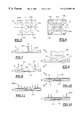
- FIG. 1 represents a card body that can be used in the method of the invention
- FIG. 2 is a cross section of an electronic module that can be used in the method of the invention
- FIG. 3 is a top view of an electronic module backing film
- FIG. 4 is a schematic view showing the arrangement of the module relative to the card
- FIG. 5 is a diagram of a cavity viewed from above with a trace for depositing glue dots
- FIG. 6 represents the gluing areas of the gluing means on the cavity after pressing
- FIGS. 7 to 12 represent the various steps of the process, or the various operating stations of a system
- FIG. 13 represents pressing means
- FIG. 14 is a top view of an example of a system for carrying out the method at high speed
- FIG. 15 shows the alcohol moistening means.
- the method of the invention requires provision of a card body with a cavity and an electronic module whose dimensions match those of the cavity.
- FIG. 1 shows an example of a smart card 1 that can be used by the process. It has a cavity 2 that can be obtained by casting at the same time as the card body, or by machining.
- Card bodies of this type are standardized by ISO and AFNOR, and accordingly have predetermined dimensions.
- the cavity must accommodate the module. It can thus have shapes that vary according to the module used.
- it is composed of two hollows: a first hollow 3 of generally rectangular shape terminating at the front surface of the card, and a second hollow 4 of generally circular shape, deeper than the first, disposed in the center of the rectangle and terminating at the bottom of the first hollow.
- the second hollow has a diameter d of 8.2 mm and a height h of 0.6 mm (FIG. 4 ).
- telephone cards or telecards are made of ABS (acrylonitrile butadiene styrene), but can also be made of PVC (polyvinyl chloride), or laminated with polycarbonate (PC), for example PC/ABS or PC/PVC.
- ABS acrylonitrile butadiene styrene
- PVC polyvinyl chloride
- PC polycarbonate
- a cavity according to the ISO standard is used, and ABS is used for the material of the card body.
- the electronic module 5 (FIGS. 2 and 3) generally has a backing film 6 a made of synthetic insulating material, contact pads 7 made of conducting material, a silicon chip 8 containing an integrated circuit, leads 9 connecting the chip to the contact pads, and a coating resin 10 covering the chip and the connecting leads.
- the coating generally thermosetting epoxy resin, forms an elevation that may have irregular dimensions, particularly of thickness.
- this elevation can be milled smooth to a more precise thickness to facilitate the operation of gluing the module into the card body.
- the goal of the invention is to use the elevation directly without milling.
- the module may be of several types, for example of the laminated leadframe type with a backing film made of polyimide or another type having an epoxy backing film.
- the module is of the laminated leadframe type and thus has a lower polyimide surface. It is supplied from a continuous film 6 b (FIG. 3) and presented on a roll.
- the cavity of the card is designed to receive the module as shown schematically in FIG. 4 .
- hollow 4 is associated with elevation 10
- hollow 3 is associated with contact pads 5 with the necessary assembly play (J). This play is such that a simple rotation of the module in the plane of the card or translation in this same plane can be detected with the naked eye and is hence a centering defect.
- At least one first gluing means able to adhere to the card body and the module is also supplied. Adhesion generally occurs after curing or treatment.
- the gluing means have the function of withstanding separating and/or bending/twisting forces according to the standards referred to above.
- the first gluing means may be of various types. It may for example be based on a liquid cyanoacrylate glue and deposited in the form of dots or beads. It can also be made of a thermoadhesive or thermoplastic material and deposited in the form of a film. It may be added to the card body or may be part thereof as for example in French Patent 2,579,799. It may be deposited on the body or on the module.
- the examples described employ a cyanoacrylate glue deposited in the cavity along a preferred trace as described below and illustrated in FIG. 5 .
- the method includes steps in which the first gluing means is deposited in the cavity or on the module, preferably in the cavity, the module is inserted into the cavity in a substantially centered position, and at least the first gluing means is pressed between the card and the module. Such steps will be described in detail in an embodiment illustrated in FIGS. 7 to 12 .
- the method of the invention is characterized by additionally having a step of supplying, and also depositing in the cavity, a second gluing means able at least to hold the module centered in the cavity (against the forces tending to shift it off-center) at least until the first gluing means is pressed.
- the second usable gluing means includes materials able to have gluing properties.
- Gluing material is understood to be a material that not only adheres to the plastics employed for the card bodies but also has a high viscosity as explained below. The adhesion must be such that the module does not peel off under the forces it encounters until pressed.
- a material one may cite in particular a single-component resin, a cyanoacrylate glue gel, a thermosetting epoxy resin, etc. These materials must also be highly viscous by comparison to a cyanoacrylate glue currently used with a viscosity of approximately 190 mP/s.
- the material is considered highly viscous by comparison to the above cyanoacrylate glue if the viscosity of the material is more than ten times the viscosity of the above cyanoacrylate glue.
- a viscosity a factor of 100 or higher is used.
- a single-component light-curable epoxy resin is used (although it is not cured in this example) which is advantageous because it has a single component and adheres well to the ABS and the polyimide module film.
- this resin is deposited in the cavity according to a step illustrated in FIG. 7 .
- the total volume of gluing material depends in particular on the spot where it is deposited (volume available in the cavity), its adhesion properties, its viscosity, and the forces it must withstand.
- It may have a total volume corresponding to a quantity of between 0.002 and 0.004 gram when deposited in a single dot. This volume may however be divided into several dots, for example four 0.001 gram dots in the case where the resin is deposited at the side in the first hollow.
- the resin that held the module very well had a viscosity of 50,000 mP/s and was deposited in the form of a drop with a volume corresponding to 0.003 gram in the center of the cavity.
- the cyanoacrylate glue used in the examples as the first gluing means is deposited in the location of the contact pads in the form of four lateral dots of glue each weighing 0.001 gram along a trace as described below.
- the resin used is preferably of the single-component thixotropic type so that it can be dispensed in a manner compatible with high manufacturing speeds.
- a relatively pure cyanoacrylate glue can be chosen, which produces its effects over a relatively long period of time in order to optimize adhesion quality, for example a time of over 60 seconds.
- the open time of the glue is approximately 60 seconds under the above environmental operating conditions. “Open time” is the time during which it is still possible to cause an object to adhere to the glue. The longer this time, the better is the polymerization. This polymerization may end where appropriate after the pressing operation.
- the embodiment of the method uses a preferred trace such as that illustrated in FIG. 5, which shows the cavity with dots 11 a to 15 a . It has a central dot 11 a in chip hollow 3 , and four other dots, known as lateral dots, 12 a to 15 a , located in hollow 4 of the contact pads and the corners of this hollow.
- the four lateral dots enable a gluing area of between 50 and 100% of the area of the cavity to be covered after pressing (FIG. 6 ). Pressing is done such that the thickness of the cyanoacrylate bond is approximately 0.02 mm.
- the print left by the spreading of each lateral dot of glue defines a semicircular area in the general shape of a “U” which extends substantially radially from near the edge of the second hollow 4 to near the corner of the rectangle delimited by the first hollow, with the base of the “U” pointing to the corner. This provides sufficient adhesion for the module to withstand the forces imposed by the standards referred to above.
- the cyanoacrylate glue is deposited just before the pressing step, and in any event after the first gluing means has been deposited. It will be understood that in this way the glue retains its maximum polymerization potential and hence adheres maximally to the module when the latter is inserted and pressed against it.
- FIGS. 7 to 12 can represent both the steps of the process and the successive operating stations of a system as described below.
- first a drop of resin 11 b is deposited in the center of the cavity with dispensing means 16 , then the card is transferred to the next station (FIG. 8 ).
- an electronic module 5 is inserted with insertion means 19 , the insertion time in this example being 300 ms but being reducible still further, and the card is transferred to the pressing station (FIG. 11 or, according to a preferred alternative, FIG. 12 ).
- the gluing means are pressed, applying a force of approximately 34 daN for 22 seconds using pressing means 20 a.
- pressing is done only at the periphery of the contact pads using pressing means 20 b , which has the advantage of pressing the glue properly with no risk of introducing mechanical stresses that could damage the semiconductor chip or the connecting leads.
- the elevation in the coating may have slightly varying thicknesses.
- the elevation may abut the bottom of the cavity and hence create a central point of the module that is slightly higher than the contact pads, which are flush with the surface of the card body.
- pressing means 20 b that can be used is described below in connection with FIG. 13 .
- the card is evacuated or undergoes pretreatment, which completes the insertion operation.
- the material of the second gluing means is used so that it produces its effects of withstanding separating and/or bending/twisting forces.
- the resin fully performs its module-holding function without exposure to ultraviolet radiation, it is preferable to cure it if only to avoid harmful microcracks under the contact pads between two prints or gluing areas 12 c to 15 c (FIG. 6 ).
- certain viscous materials such as the resin above or a cyanoacrylate glue gel advantageously exhibit properties of mechanical resistance to separating and/or bending/twisting forces.
- the method according to the first embodiment has an additional step during which polymerization is initiated by subjecting the epoxy resin to ultraviolet radiation, with this step preceding insertion of the module.
- this step is preferably carried out (FIG. 9) just after the step in which the drop of resin described above is deposited.
- the intensity and duration of exposure are regulated here such that the open time of the resin is greater than 60 seconds, with this time corresponding to that of the cyanoacrylate glue used.
- the exposure time ranges from 0 . 5 to 1 second.
- the intensity can be regulated both by the power of the bulb used and by the distance from the resin.
- the resin can be irradiated later at the same time the drops of cyanoacrylate glue are deposited.
- the gap in time between activation of the first and second gluing means and the pressing step is minimized, as only one station separates it from the pressing station, so that better-quality gluing can be done as the pressing time is maximized relative to the open time of each gluing means.
- a cyanoacrylate glue gel is used instead of the epoxy resin.
- This gel also has properties allowing the module to hold firm while subjected to forces pushing it off-center during manufacture.
- the film of the module can be treated by moistening with alcohol to initiate polymerization of the cyanoacrylate glue gel in contact with the module. Such means are described in FIG. 15 .
- the insertion and pressing steps are identical to those described for the resin.
- card supply means 21 for supplying a plurality of card bodies, module supply means 22 a , 22 b for supplying a plurality of modules, a resin drop dispensing station 23 equipped with resin dispensing means 23 b , an ultraviolet irradiation station 24 equipped with ultraviolet irradiation means 24 b , a cyanoacrylate glue drop dispensing station 25 equipped with dispensing means 25 b having two needles 16 and 17 , a module insertion station 26 equipped with insertion means 26 b , pressing stations 27 equipped with pressing means 27 a disposed at the periphery of a carousel 28 which supports the cards during the pressing time, means 29 for cutting up the modules and transferring them to the insertion station, means 30 for moistening with alcohol if appropriate, then removal means 31 .
- the system also includes an enclosure with controlled temperature and relative humidity (not shown).
- the supply means are two rolls, a first roll 22 a loaded with a film 6 a supporting the modules and a second roll 22 b supporting the film from which modules are absent, one paying out while the other winds up. If appropriate, the film passes by means 30 for moistening with alcohol described hereinbelow before passing by module cutting means 29 .
- Resin dispensing means 23 have a hollow needle 16 which can move up and down.
- the irradiation station is connected to ultraviolet (UV) radiation generating means of a known type employing elongate optical means 32 (FIG. 9) able to bring the radiation (UV) to a point near the resin in such a way as to expose only the cavity to radiation, as certain marks on the card are sensitive to ultraviolet radiation.
- UV radiation generating means of a known type employing elongate optical means 32 (FIG. 9) able to bring the radiation (UV) to a point near the resin in such a way as to expose only the cavity to radiation, as certain marks on the card are sensitive to ultraviolet radiation.
- the cyanoacrylate glue dispensing means have two hollow needles 17 , 18 (FIG. 8) which can move vertically and transversely.
- the modules are extracted from film 6 a by cutting means and taken with the aid of transfer means 29 to the insertion station where they are inserted in the center of the cavity of each card. It is especially during the film-cutting operation that residual strains are released and are responsible for the curving of the module as explained above.
- Each pressing station 27 is provided with pressing means 27 a having a vertically movable end 20 a (FIG. 13) that comes in contact with the module.
- this end is provided with a blanket 20 b with a hole in the middle so that pressure can be applied only to the periphery of the module.
- the blanket is made of an elastomer material able to distribute the pressure without affecting the contact pads. It is rectangular in shape, corresponding to the shape of the module.
- the diameter of the central hole 20 c corresponds substantially to the diameter of the second hollow.
- the means 30 for moistening the lower surface of the module with alcohol are in this example a sponge 32 dipping into a bath 33 of 95° ethyl alcohol in a container.
- the sponge is kept continuously in contact with the module supply film.
- the means of moving the cards from one station to the other are mechanized to produce a rate of at least 2000 cards per hour.
- dispensing needle 16 When a card arrives at resin dispensing station 23 , dispensing needle 16 is positioned above the location of central point 11 a corresponding to the intended trace (FIG. 5) then descends to near the surface of the cavity, and a control system (not shown) causes 0.003 gram of resin to be delivered and deposited in the cavity; the needle then rises in such a way as to break off a filament of residual resin that tends to cling to the needle and returns to the standby position awaiting the next card.
- the control means are set to allow descent, dispensing, and rising in 1.5 seconds, after which the cards are transferred to irradiation station 24 .
- the resin is exposed to ultraviolet radiation (UV) for 0.5 to 1 second to allow a resin open time of 60 seconds, and the cards are transferred to station 25 dispensing cyanoacrylate drops.
- UV ultraviolet radiation
- two needles 17 and 18 are positioned at points 12 a corresponding to the intended trace, are lowered, dispense four 0.001 gram drops which are deposited on the cavity, then rise to await the next cards, and the cards are transferred to insertion station 26 b.
- the cards receive a module, the insertion time being 300 ms, and the cards are transferred to pressing station 27 .
- each module is pressed against the card body, the force applied being 34 daN.
- the cards stay on the carousel for 22 seconds and are then ejected to the next station.
- the cards may be tested and sent to storage means 31 .
Abstract
Description
Claims (12)
Applications Claiming Priority (2)
| Application Number | Priority Date | Filing Date | Title |
|---|---|---|---|
| PCT/FR1996/001246 WO1998006062A1 (en) | 1996-08-05 | 1996-08-05 | Improvement to a method for making smart cards, and resulting cards |
| CA 2262481 CA2262481A1 (en) | 1996-08-05 | 1996-08-05 | Improvement to a method for making smart cards, and resulting cards |
Publications (1)
| Publication Number | Publication Date |
|---|---|
| US6223989B1 true US6223989B1 (en) | 2001-05-01 |
Family
ID=25680827
Family Applications (1)
| Application Number | Title | Priority Date | Filing Date |
|---|---|---|---|
| US09/230,850 Expired - Lifetime US6223989B1 (en) | 1996-08-05 | 1996-08-05 | Method for making smart cards, and resulting cards |
Country Status (9)
| Country | Link |
|---|---|
| US (1) | US6223989B1 (en) |
| EP (1) | EP0917687B1 (en) |
| JP (1) | JP2001505329A (en) |
| AT (1) | ATE200715T1 (en) |
| AU (1) | AU707828B2 (en) |
| CA (1) | CA2262481A1 (en) |
| DE (1) | DE69612574T2 (en) |
| ES (1) | ES2159061T3 (en) |
| WO (1) | WO1998006062A1 (en) |
Cited By (11)
| Publication number | Priority date | Publication date | Assignee | Title |
|---|---|---|---|---|
| US6390375B2 (en) * | 1999-11-29 | 2002-05-21 | Ask S.A. | Contactless or hybrid contact-contactless smart card designed to limit the risks of fraud |
| US6513718B1 (en) * | 1999-05-06 | 2003-02-04 | Oberthur Card Systems Sas | Method for mounting a microcircuit in a cavity of a card forming a support and resulting card |
| US6536674B2 (en) | 1999-11-29 | 2003-03-25 | Ask S.A. | Process for manufacturing a contactless smart card with an antenna support made of fibrous material |
| US6651891B1 (en) * | 1997-11-04 | 2003-11-25 | Elke Zakel | Method for producing contactless chip cards and corresponding contactless chip card |
| US20120138691A1 (en) * | 2010-12-06 | 2012-06-07 | Oberthur Technologies | Method of receiving a module in a smart card body |
| US8649820B2 (en) | 2011-11-07 | 2014-02-11 | Blackberry Limited | Universal integrated circuit card apparatus and related methods |
| USD701864S1 (en) | 2012-04-23 | 2014-04-01 | Blackberry Limited | UICC apparatus |
| USD702240S1 (en) | 2012-04-13 | 2014-04-08 | Blackberry Limited | UICC apparatus |
| US8936199B2 (en) | 2012-04-13 | 2015-01-20 | Blackberry Limited | UICC apparatus and related methods |
| CN110126261A (en) * | 2019-06-11 | 2019-08-16 | 深圳市深科达智能装备股份有限公司 | Display or touch module 3D printing glue-line method |
| CN111463583A (en) * | 2019-01-18 | 2020-07-28 | 泰连德国有限公司 | Electrical connection assembly having cyanoacrylate adhesive layer between soldered conductors and method |
Families Citing this family (4)
| Publication number | Priority date | Publication date | Assignee | Title |
|---|---|---|---|---|
| FR2800087A1 (en) * | 1999-10-26 | 2001-04-27 | Gemplus Card Int | Bonding different polymers comprises using compatible material, used for silicon chip cards in mobile phones, as intermediate layer between one polymer and adhesive layer applied to the other polymer |
| FR2823888B1 (en) * | 2001-04-24 | 2005-02-18 | Gemplus Card Int | METHOD FOR MANUFACTURING CONTACTLESS OR HYBRID CARD AND OBTAINED CARD |
| DE102006050564A1 (en) | 2006-10-26 | 2008-04-30 | Grönemeyer Medical GmbH & Co. KG | Operating table panel has one or more base sections and one or more modules, where modules and base sections are adjustable relative to each other and modules are designed such that they are separated from operating table panel |
| US20120304531A1 (en) | 2011-05-30 | 2012-12-06 | Shell Oil Company | Liquid fuel compositions |
Citations (8)
| Publication number | Priority date | Publication date | Assignee | Title |
|---|---|---|---|---|
| FR2579799A1 (en) * | 1985-03-28 | 1986-10-03 | Flonic Sa | METHOD FOR MANUFACTURING ELECTRONIC MEMORY CARDS AND CARDS OBTAINED ACCORDING TO SAID METHOD |
| US4871405A (en) | 1988-03-30 | 1989-10-03 | Director General, Agency Of Industrial Science And Technology | Method of bonding a semiconductor to a package with a low and high viscosity bonding agent |
| US4903118A (en) | 1988-03-30 | 1990-02-20 | Director General, Agency Of Industrial Science And Technology | Semiconductor device including a resilient bonding resin |
| US5169056A (en) | 1992-02-21 | 1992-12-08 | Eastman Kodak Company | Connecting of semiconductor chips to circuit substrates |
| EP0717371A2 (en) | 1994-12-15 | 1996-06-19 | ODS, R. OLDENBOURG DATENSYSTEME GmbH | Manufacturing method and device for chip cards and chip card |
| US5612532A (en) * | 1993-09-01 | 1997-03-18 | Kabushiki Kaisha Toshiba | Thin IC card and method for producing the same |
| US5671525A (en) * | 1995-02-13 | 1997-09-30 | Gemplus Card International | Method of manufacturing a hybrid chip card |
| US5776278A (en) * | 1992-06-17 | 1998-07-07 | Micron Communications, Inc. | Method of manufacturing an enclosed transceiver |
Family Cites Families (1)
| Publication number | Priority date | Publication date | Assignee | Title |
|---|---|---|---|---|
| DE4229639C1 (en) * | 1992-09-04 | 1993-12-09 | Tomas Meinen | IC card manufacturing method - delivering volume of adhesive determined by variation of pressure and duration in which adhesive is supplied via tubule |
-
1996
- 1996-08-05 WO PCT/FR1996/001246 patent/WO1998006062A1/en not_active Application Discontinuation
- 1996-08-05 DE DE1996612574 patent/DE69612574T2/en not_active Expired - Lifetime
- 1996-08-05 AU AU46880/97A patent/AU707828B2/en not_active Ceased
- 1996-08-05 US US09/230,850 patent/US6223989B1/en not_active Expired - Lifetime
- 1996-08-05 JP JP50765198A patent/JP2001505329A/en active Pending
- 1996-08-05 ES ES96946394T patent/ES2159061T3/en not_active Expired - Lifetime
- 1996-08-05 AT AT96946394T patent/ATE200715T1/en not_active IP Right Cessation
- 1996-08-05 EP EP19960946394 patent/EP0917687B1/en not_active Expired - Lifetime
- 1996-08-05 CA CA 2262481 patent/CA2262481A1/en not_active Abandoned
Patent Citations (8)
| Publication number | Priority date | Publication date | Assignee | Title |
|---|---|---|---|---|
| FR2579799A1 (en) * | 1985-03-28 | 1986-10-03 | Flonic Sa | METHOD FOR MANUFACTURING ELECTRONIC MEMORY CARDS AND CARDS OBTAINED ACCORDING TO SAID METHOD |
| US4871405A (en) | 1988-03-30 | 1989-10-03 | Director General, Agency Of Industrial Science And Technology | Method of bonding a semiconductor to a package with a low and high viscosity bonding agent |
| US4903118A (en) | 1988-03-30 | 1990-02-20 | Director General, Agency Of Industrial Science And Technology | Semiconductor device including a resilient bonding resin |
| US5169056A (en) | 1992-02-21 | 1992-12-08 | Eastman Kodak Company | Connecting of semiconductor chips to circuit substrates |
| US5776278A (en) * | 1992-06-17 | 1998-07-07 | Micron Communications, Inc. | Method of manufacturing an enclosed transceiver |
| US5612532A (en) * | 1993-09-01 | 1997-03-18 | Kabushiki Kaisha Toshiba | Thin IC card and method for producing the same |
| EP0717371A2 (en) | 1994-12-15 | 1996-06-19 | ODS, R. OLDENBOURG DATENSYSTEME GmbH | Manufacturing method and device for chip cards and chip card |
| US5671525A (en) * | 1995-02-13 | 1997-09-30 | Gemplus Card International | Method of manufacturing a hybrid chip card |
Cited By (15)
| Publication number | Priority date | Publication date | Assignee | Title |
|---|---|---|---|---|
| US6651891B1 (en) * | 1997-11-04 | 2003-11-25 | Elke Zakel | Method for producing contactless chip cards and corresponding contactless chip card |
| US6513718B1 (en) * | 1999-05-06 | 2003-02-04 | Oberthur Card Systems Sas | Method for mounting a microcircuit in a cavity of a card forming a support and resulting card |
| US6390375B2 (en) * | 1999-11-29 | 2002-05-21 | Ask S.A. | Contactless or hybrid contact-contactless smart card designed to limit the risks of fraud |
| US6536674B2 (en) | 1999-11-29 | 2003-03-25 | Ask S.A. | Process for manufacturing a contactless smart card with an antenna support made of fibrous material |
| US20120138691A1 (en) * | 2010-12-06 | 2012-06-07 | Oberthur Technologies | Method of receiving a module in a smart card body |
| US8544756B2 (en) * | 2010-12-06 | 2013-10-01 | Oberthur Technologies | Method of receiving a module in a smart card body |
| US8649820B2 (en) | 2011-11-07 | 2014-02-11 | Blackberry Limited | Universal integrated circuit card apparatus and related methods |
| USD702240S1 (en) | 2012-04-13 | 2014-04-08 | Blackberry Limited | UICC apparatus |
| USD703208S1 (en) | 2012-04-13 | 2014-04-22 | Blackberry Limited | UICC apparatus |
| US8936199B2 (en) | 2012-04-13 | 2015-01-20 | Blackberry Limited | UICC apparatus and related methods |
| USD701864S1 (en) | 2012-04-23 | 2014-04-01 | Blackberry Limited | UICC apparatus |
| USD702241S1 (en) * | 2012-04-23 | 2014-04-08 | Blackberry Limited | UICC apparatus |
| CN111463583A (en) * | 2019-01-18 | 2020-07-28 | 泰连德国有限公司 | Electrical connection assembly having cyanoacrylate adhesive layer between soldered conductors and method |
| CN110126261A (en) * | 2019-06-11 | 2019-08-16 | 深圳市深科达智能装备股份有限公司 | Display or touch module 3D printing glue-line method |
| CN110126261B (en) * | 2019-06-11 | 2021-04-13 | 深圳市深科达智能装备股份有限公司 | Method for 3D printing of adhesive layer by display or touch module |
Also Published As
| Publication number | Publication date |
|---|---|
| DE69612574D1 (en) | 2001-05-23 |
| WO1998006062A1 (en) | 1998-02-12 |
| JP2001505329A (en) | 2001-04-17 |
| DE69612574T2 (en) | 2001-10-18 |
| EP0917687A1 (en) | 1999-05-26 |
| ES2159061T3 (en) | 2001-09-16 |
| ATE200715T1 (en) | 2001-05-15 |
| AU707828B2 (en) | 1999-07-22 |
| CA2262481A1 (en) | 1998-02-12 |
| EP0917687B1 (en) | 2001-04-18 |
| AU4688097A (en) | 1998-02-25 |
Similar Documents
| Publication | Publication Date | Title |
|---|---|---|
| US6223989B1 (en) | Method for making smart cards, and resulting cards | |
| CN1214344C (en) | Method for making electronic module or label, resulting electronic module or label and medium containing such a module or label | |
| KR100605475B1 (en) | Method for making smart cards using isotropic thermoset adhesive materials | |
| EP0030827A1 (en) | Decorative emblem and method of manufacture | |
| US4925714A (en) | Coextruded core laminates | |
| US5542171A (en) | Method of selectively releasing plastic molding material from a surface | |
| EP0339616B1 (en) | Apparatus for manufacturing optical information recording medium | |
| EP0249266A1 (en) | Data-carrying card, method for producing such a card, and device for carrying out said method | |
| GB2026430A (en) | Method and apparatus for bonding components together | |
| US6554598B1 (en) | Mold assembly for encapsulating semiconductor device | |
| JPS5971819A (en) | Fixture for base cup | |
| US6306240B1 (en) | Method for making smart cards, and resulting cards | |
| US20050253228A1 (en) | Method for encapsulation of a chipcard and module obtained thus | |
| US6402880B1 (en) | Method of gluing together first and second disc elements in the manufacture of a DVD | |
| CN1149920A (en) | Pass card or the like in the form of smart card | |
| CN102431951A (en) | Double-carrier and double-MEMS (micro-electro-mechanical systems) device package and production method thereof | |
| CN106653707A (en) | Fingerprint identification module and packaging method | |
| CN106653708A (en) | Fingerprint identification module and packaging method thereof | |
| JPH027466Y2 (en) | ||
| CN1137512C (en) | Method for making smart cards and resulting cards | |
| CN100452089C (en) | Method for making an electronic module or label and medium containing such module or label | |
| US4309237A (en) | Apparatus for adhering a can opening key to a container | |
| EP0215502B1 (en) | Method of forming a semiconductor component with attached component bonding adhesive | |
| CN219626627U (en) | Carrier plate for chip packaging | |
| KR20000029845A (en) | Method for making smart cards and resulting cards |
Legal Events
| Date | Code | Title | Description |
|---|---|---|---|
| AS | Assignment |
Owner name: GEMPLUS S.C.A., FRANCE Free format text: ASSIGNMENT OF ASSIGNORS INTEREST;ASSIGNOR:PERMINGEAT, VINCENT;REEL/FRAME:009803/0819 Effective date: 19990219 |
|
| STCF | Information on status: patent grant |
Free format text: PATENTED CASE |
|
| FEPP | Fee payment procedure |
Free format text: PAYOR NUMBER ASSIGNED (ORIGINAL EVENT CODE: ASPN); ENTITY STATUS OF PATENT OWNER: LARGE ENTITY |
|
| FPAY | Fee payment |
Year of fee payment: 4 |
|
| REMI | Maintenance fee reminder mailed | ||
| FPAY | Fee payment |
Year of fee payment: 8 |
|
| AS | Assignment |
Owner name: GEMPLUS SA, FRANCE Free format text: MERGER;ASSIGNOR:GEMPLUS SCA;REEL/FRAME:024900/0648 Effective date: 19991207 |
|
| AS | Assignment |
Owner name: GEMALTO SA, FRANCE Free format text: MERGER;ASSIGNOR:GEMPLUS SA;REEL/FRAME:025486/0743 Effective date: 20081001 |
|
| FPAY | Fee payment |
Year of fee payment: 12 |