US6236256B1 - Voltage level converters - Google Patents

Voltage level converters Download PDF

Info

Publication number
US6236256B1
US6236256B1 US09/272,267 US27226799A US6236256B1 US 6236256 B1 US6236256 B1 US 6236256B1 US 27226799 A US27226799 A US 27226799A US 6236256 B1 US6236256 B1 US 6236256B1
Authority
US
United States
Prior art keywords
input
voltage
voltage level
time period
circuit node
Prior art date
Legal status (The legal status is an assumption and is not a legal conclusion. Google has not performed a legal analysis and makes no representation as to the accuracy of the status listed.)
Expired - Fee Related
Application number
US09/272,267
Inventor
Michael James Brownlow
Graham Andrew Cairns
Current Assignee (The listed assignees may be inaccurate. Google has not performed a legal analysis and makes no representation or warranty as to the accuracy of the list.)
Sharp Corp
Original Assignee
Sharp Corp
Priority date (The priority date is an assumption and is not a legal conclusion. Google has not performed a legal analysis and makes no representation as to the accuracy of the date listed.)
Filing date
Publication date
Application filed by Sharp Corp filed Critical Sharp Corp
Assigned to SHARP KABUSHIKI KAISHA reassignment SHARP KABUSHIKI KAISHA ASSIGNMENT OF ASSIGNORS INTEREST (SEE DOCUMENT FOR DETAILS). Assignors: BROWNLOW, MICHAEL JAMES, CAIRNS, GRAHAM ANDREW
Application granted granted Critical
Publication of US6236256B1 publication Critical patent/US6236256B1/en
Anticipated expiration legal-status Critical
Expired - Fee Related legal-status Critical Current

Links

Images

Classifications

    • HELECTRICITY
    • H03ELECTRONIC CIRCUITRY
    • H03KPULSE TECHNIQUE
    • H03K17/00Electronic switching or gating, i.e. not by contact-making and –breaking
    • H03K17/51Electronic switching or gating, i.e. not by contact-making and –breaking characterised by the components used
    • H03K17/56Electronic switching or gating, i.e. not by contact-making and –breaking characterised by the components used by the use, as active elements, of semiconductor devices
    • H03K17/60Electronic switching or gating, i.e. not by contact-making and –breaking characterised by the components used by the use, as active elements, of semiconductor devices the devices being bipolar transistors
    • GPHYSICS
    • G09EDUCATION; CRYPTOGRAPHY; DISPLAY; ADVERTISING; SEALS
    • G09GARRANGEMENTS OR CIRCUITS FOR CONTROL OF INDICATING DEVICES USING STATIC MEANS TO PRESENT VARIABLE INFORMATION
    • G09G3/00Control arrangements or circuits, of interest only in connection with visual indicators other than cathode-ray tubes
    • G09G3/20Control arrangements or circuits, of interest only in connection with visual indicators other than cathode-ray tubes for presentation of an assembly of a number of characters, e.g. a page, by composing the assembly by combination of individual elements arranged in a matrix no fixed position being assigned to or needed to be assigned to the individual characters or partial characters
    • G09G3/34Control arrangements or circuits, of interest only in connection with visual indicators other than cathode-ray tubes for presentation of an assembly of a number of characters, e.g. a page, by composing the assembly by combination of individual elements arranged in a matrix no fixed position being assigned to or needed to be assigned to the individual characters or partial characters by control of light from an independent source
    • G09G3/36Control arrangements or circuits, of interest only in connection with visual indicators other than cathode-ray tubes for presentation of an assembly of a number of characters, e.g. a page, by composing the assembly by combination of individual elements arranged in a matrix no fixed position being assigned to or needed to be assigned to the individual characters or partial characters by control of light from an independent source using liquid crystals
    • G09G3/3611Control of matrices with row and column drivers
    • G09G3/3685Details of drivers for data electrodes
    • G09G3/3688Details of drivers for data electrodes suitable for active matrices only
    • HELECTRICITY
    • H03ELECTRONIC CIRCUITRY
    • H03KPULSE TECHNIQUE
    • H03K19/00Logic circuits, i.e. having at least two inputs acting on one output; Inverting circuits
    • H03K19/0175Coupling arrangements; Interface arrangements
    • H03K19/0185Coupling arrangements; Interface arrangements using field effect transistors only
    • H03K19/018507Interface arrangements
    • H03K19/01855Interface arrangements synchronous, i.e. using clock signals
    • HELECTRICITY
    • H03ELECTRONIC CIRCUITRY
    • H03KPULSE TECHNIQUE
    • H03K3/00Circuits for generating electric pulses; Monostable, bistable or multistable circuits
    • H03K3/01Details
    • H03K3/012Modifications of generator to improve response time or to decrease power consumption
    • HELECTRICITY
    • H03ELECTRONIC CIRCUITRY
    • H03KPULSE TECHNIQUE
    • H03K3/00Circuits for generating electric pulses; Monostable, bistable or multistable circuits
    • H03K3/02Generators characterised by the type of circuit or by the means used for producing pulses
    • H03K3/353Generators characterised by the type of circuit or by the means used for producing pulses by the use, as active elements, of field-effect transistors with internal or external positive feedback
    • H03K3/356Bistable circuits
    • H03K3/356104Bistable circuits using complementary field-effect transistors
    • H03K3/356113Bistable circuits using complementary field-effect transistors using additional transistors in the input circuit
    • H03K3/356121Bistable circuits using complementary field-effect transistors using additional transistors in the input circuit with synchronous operation
    • HELECTRICITY
    • H03ELECTRONIC CIRCUITRY
    • H03KPULSE TECHNIQUE
    • H03K3/00Circuits for generating electric pulses; Monostable, bistable or multistable circuits
    • H03K3/02Generators characterised by the type of circuit or by the means used for producing pulses
    • H03K3/353Generators characterised by the type of circuit or by the means used for producing pulses by the use, as active elements, of field-effect transistors with internal or external positive feedback
    • H03K3/356Bistable circuits
    • H03K3/356104Bistable circuits using complementary field-effect transistors
    • H03K3/356113Bistable circuits using complementary field-effect transistors using additional transistors in the input circuit
    • H03K3/356147Bistable circuits using complementary field-effect transistors using additional transistors in the input circuit using pass gates
    • H03K3/356156Bistable circuits using complementary field-effect transistors using additional transistors in the input circuit using pass gates with synchronous operation
    • GPHYSICS
    • G09EDUCATION; CRYPTOGRAPHY; DISPLAY; ADVERTISING; SEALS
    • G09GARRANGEMENTS OR CIRCUITS FOR CONTROL OF INDICATING DEVICES USING STATIC MEANS TO PRESENT VARIABLE INFORMATION
    • G09G2310/00Command of the display device
    • G09G2310/02Addressing, scanning or driving the display screen or processing steps related thereto
    • G09G2310/0264Details of driving circuits
    • G09G2310/027Details of drivers for data electrodes, the drivers handling digital grey scale data, e.g. use of D/A converters
    • GPHYSICS
    • G09EDUCATION; CRYPTOGRAPHY; DISPLAY; ADVERTISING; SEALS
    • G09GARRANGEMENTS OR CIRCUITS FOR CONTROL OF INDICATING DEVICES USING STATIC MEANS TO PRESENT VARIABLE INFORMATION
    • G09G2310/00Command of the display device
    • G09G2310/02Addressing, scanning or driving the display screen or processing steps related thereto
    • G09G2310/0264Details of driving circuits
    • G09G2310/0294Details of sampling or holding circuits arranged for use in a driver for data electrodes

Landscapes

  • Engineering & Computer Science (AREA)
  • Computer Hardware Design (AREA)
  • Physics & Mathematics (AREA)
  • Chemical & Material Sciences (AREA)
  • General Engineering & Computer Science (AREA)
  • Mathematical Physics (AREA)
  • Computing Systems (AREA)
  • Crystallography & Structural Chemistry (AREA)
  • General Physics & Mathematics (AREA)
  • Theoretical Computer Science (AREA)
  • Logic Circuits (AREA)
  • Semiconductor Integrated Circuits (AREA)
  • Thin Film Transistor (AREA)

Abstract

A voltage level converter for converting an input signal at a first voltage level to an output signal at a second voltage level, the converter comprises: an input for receiving said input signal; an output for outputting said output signal; a circuit node; precharge means for charging or discharging said circuit node to a third voltage level during a first time period by connection of said circuit node to a first voltage supply; isolation means for isolating said circuit node from said first voltage supply during a second time period; input means for changing the voltage at said circuit node in dependence on the voltage at said input during a third time period; and output means arranged so that the voltage at said output depends on the voltage at said circuit node.

Description

TECHNICAL FIELD OF THE INVENTION
The invention relates to voltage level converters, and is useful in inter alia high speed CMOS circuits which receive many data inputs at a voltage significantly less than the supply voltage. The invention is of particular use in the field of monolithic digital data drivers for active matrix displays. In these circuits low performance TFT circuitry requires a high supply voltage to achieve the necessary speed of operation, whereas to minimise power consumption low voltage inputs are desirable.
DESCRIPTION OF THE RELATED ART
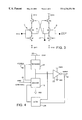
The simplest. type of prior art digital level shifter is shown in FIG. 1, and described in detail in A. Bellaouar, M. Elmasry. Low Power Digital VLSI Design. Kluwer Academic Publishers, 1995. The circuit consists of two CMOS inverters 2 and 4, each comprising a p-type (PMOS) transistor M1, M3 and an n-type (NMOS) transistor M2, M4. The first CMOS inverter 2 is powered by a supply voltage VDD1, and the second CMOS inverter 4 is powered by a larger supply voltage VDD2. The main disadvantage of this circuit is that the power consumption is considerable since both transistors M3 and M4 in the second inverter 4 conduct when the output of the first inverter 2 is high, ie. equal to VDD1. One of the basic criteria for minimising power consumption is that there should be no direct current path between the supply voltages and ground.
A further prior art circuit is shown in FIG. 2, and described in detail in U.S. Pat. No. 4,486,670. This circuit overcomes the problem of direct power consumption by using a latch (consisting of the four transistors M5, M6, M7 and M8) to ensure that if one of the complementary transistors M3 or M4 is turned on, the other is turned off.
A widely used level shift circuit with improved latching action is shown in the prior art circuit of FIG. 3, and described in detail in U.S. Pat. No. 4,845,381. Two CMOS inverters 6 and 8, made up of transistors M1, M2 and M4, M5 respectively, receive complementary digital input signals INPUT and INPUT*, varying between voltages of VDD1 and GND. The outputs 9 and 11 of the inverters 6 and 8 are cross-coupled and applied to the gates of the p-type transistors M3 and M6 which control the supply of a higher voltage VDD2 to the inverters 6 and 8. If the input signal INPUT is at VDD1 (ie. logic high) and the complementary input INPUT* is at ground, then transistors M1, M5 and M6 are on whilst transistors M2, M3 and M4 are off. Thus the output 13 of the shift circuit as a whole is at voltage VDD2 (ie. logic high). The main limitation of this approach for large numbers of inputs is the need to supply two complementary input signals.
SUMMARY OF THE INVENTION
According to the invention there is provided a voltage level converter for converting an input signal at a first voltage level to an output signal at a second voltage level, the converter comprising an input for receiving said input signal, an output for outputting said output signal, a circuit node, precharge means for charging or discharging said circuit node to a third voltage level during a first time period by connection of said circuit node to a first voltage supply, isolation means for isolating said circuit node from said first voltage supply during a second time period, input means for changing the voltage at said circuit node in dependence on the voltage at said input during a third time period, and output means arranged so that the voltage at said output depends on the voltage at said circuit node.
Such a level converter does not require a complementary input signal, which is particularly advantageous if a number of such level converters are used in an arrangement having a large number of inputs. In addition, the isolation means can be used to prevent a direct current path from the first voltage supply to ground, thus reducing power consumption.
Said third voltage level may be substantially equal to said second voltage level.
This allows said first voltage supply to be used for both said output signal and for charging or discharging said circuit node.
Said third time period may coincide with, or lie within, said second time period.
The voltage level converter may further comprise an input node which is charged or discharged to a fourth voltage level during said first time period by connection of said input node to a second voltage supply.
Said isolation means may isolate said input node from said second voltage supply during said second time period.
Said second voltage supply may be negatively biased with respect to said input signal.
Said isolation means may comprise a first isolation field effect transistor the source and drain of which are connected between said second voltage supply and said input node.
Said isolation means may comprise a second isolation field effect transistor the source and drain of which are connected between said first voltage supply and said circuit node.
Said input means may comprise a sampler for sampling said input signal during said third time period.
Said sampler may comprise a sampling field effect transistor the gate of which is connected to a sampling signal.
The source and drain of said sampling field effect transistor may be connected between said input and said input node.
The voltage level converter may further comprise a latch for latching said output signal at the voltage determined by said input means.
The voltage level converter may further comprise a feedback field effect transistor, the source and drain of which are connected between said first voltage supply and said input node, and the gate of which is connected to said circuit node.
This provides the advantage of increased switching speed of the level converter, by increasing the switching speed of the input transistor mentioned below.
Said output means may comprise a CMOS inverter, the input of which is connected to said circuit node.
Said input means may comprise an input field effect transistor arranged to discharge said circuit node if said input signal is at a logic high level during said third time period.
The source and drain of said input field effect tristor may be connected between said circuit node and said second voltage supply, and the gate of said input field effect transistor may be connected to said input node.
The source of said input field effect transistor may be connected to said second voltage supply.
This provides the advantage that, if said second voltage supply is negatively biased with respect to said input signal, the drive efficacy of the input signal is increased.
The gate of said input field effect transistor may be connected to said negative voltage supply during said first time period, and isolated from said negative supply during said second time period.
Said input and output signals may be digital signals.
The invention also provides an active matrix liquid crystal display comprising a voltage level converter as described above.
BRIEF DESCRIPTION OF THE DRAWINGS
Embodiments of the invention will now be described, by way of example only, with reference to the accompanying drawings, in which:
FIGS. 1 to 3 show three prior art level converters, as discussed above;
FIG. 4 shows a block diagram illustrating the basic components of an embodiment of the invention;
FIG. 5 shows a specific circuit level schematic of one embodiment of the invention;
FIG. 6 shows a simulation of voltages in the circuit of FIG. 5; and
FIGS. 7A and 7B are a schematic view of an active matrix display and associated data and scan drivers.
DETAILED DESCRIPTION OF THE INVENTION
The basic components of an embodiment of the invention are shown in FIG. 4. A digital input signal 10, varying between ground and a voltage VDD1 (for logic levels 0 and 1 respectively) is converted to a digital output signal 12, varying between ground and a higher voltage VDD2. Precharge and evaluate blocks 14 and 16 respectively are controlled by a control signal 18. The precharge block 14 charges node A to voltage VDD2 during a standby phase, by connecting node A to a voltage supply 20. The precharge block 14 subsequently isolates node A from the voltage supply 20 during an active phase.
During the active phase, the input signal 10 is sampled by the evaluate block 16. If the input signal 10 is high, then the evaluate block 16 discharges node A, and an inverter 22 produces a high output signal 12, which is at the voltage VDD2. The evaluate block 16 and the inverter 22 are connected to a bias voltage VSS1 which is negative with respect to the ground voltage (corresponding with the input signal logic level 0) mentioned above. The negative bias voltage VSSI increases the drive efficacy and switching speed of the evaluate block 16. A latch 24 is also provided in order to latch the output signal 12 at a high level once node A has been discharged.
If the sampled input signal 10 is low, then the evaluate block 16 does not discharge node A, and the output signal 12 remains low (ie. at ground).
FIG. 5 illustrates one way of implementing the arrangement of FIG. 4 using seven field effect transistors M1 to M7 to form a digital data interface 30. Transistor M1 is an input sampling transistor controlled by a signal SAMPLE in order to sample an input signal INPUT. The input signal INPUT is a digital signal varying between ground and a low voltage level (eg. 3.3 volts) representing logic states 0 and 1 respectively. The digital data interface 30 of FIG. 5 converts the digital input signal to a digital output signal OUTPUT which varies between ground and a higher voltage level VDD, typically around 12 volts. Transistors M5 and M6 form a conventional CMOS inverter, of which node A forms the input Transistors M3 and M4 form a precharge—evaluate type inverter, and M7 is a feedback transistor. M7 can be regarded as forming part of the latch 24 of FIG. 4.
The gates of NMOS transistor M2 and PMOS transistor M3 are respectively connected to a precharge signal PRECHARGE and a complementary signal PRECHARGE*. M2 can be regarded as forming part of the precharge block 14 of FIG. 4.
The sources of NMOS transistors M2 and M4 are connected to a negative source bias supply VB, of magnitude less than the threshold voltage of the n-type transistors M2 and M4.
The digital data interface 30 of FIG. 5 operates as follows:
1. In a standby phase the PRECHARGE signal is high NMOS transistor M2 discharges the gate of NMOS transistor M4 (node B), while PMOS transistor M3 charges the input (node A) of the output CMOS inverter (M5, M6) up to voltage VDD. In this condition there is no conducting path from the supply voltage VDD to ground so quiescent power consumption is determined only by leakage currents in M4 and M5.
2. In a subsequent active phase the PRECHARGE signal goes low, isolating node A from the power supply voltage VDD by switching off M3. Similarly node B is isolated from the negative supply voltage VB because M2 is switched off. Nodes A and B therefore remain high and low respectively.
3. Next the SAMPLE signal goes momentarily high, switching on M1 and charging node B to the voltage currently on the data input line 32. The SAMPLE signal then goes low, isolating node B from the input.
4. If the sampled input signal is low, ie. OV, then the gate-source voltage across M4 remains below threshold and so the input transistor M4 does not conduct. Node A therefore remains at the precharged high voltage and the output remains low.
5. If the sampled input signal is high (e.g. 3.3V) then the gate-source voltage of the input transistor M4 is equal to the logic high voltage (eg. 3.3V) minus the negative source bias voltage VB. Because this potential exceeds the threshold voltage of M4, M4 begins to conduct. As M4 discharges node A, the feedback transistor M7 begins to turn on as a result of the dropping voltage at its gate, thus charging node B higher. This turns on M4 harder and node A discharges more quickly. The final state of the circuit is with node B equal to VDD and node A equal to the source bias voltage VB. In this state there is no quiescent power consumption, apart from leakage effects, and the output is at VDD, ie. high.
The low voltage input signal is able to drive the output significantly faster than the prior art because the load transistor M3 can only conduct in the standby state, and the input transistor M4 therefore only has to conditionally discharge the capacitance at the output node A. The negative source bias voltage VB also increases the switching speed by creating a larger gate overdrive for the input transistor M4.
The use of a low input data voltage inherently reduces the power consumption resulting from the input signals driving parasitic capacitances. The power consumption of the interface 30 is also low because the dynamic technique avoids simultaneous conduction of the input and load transistors M4 and M3. Furthermore, the DC power consumption is negligible in both the precharged state and the latched state.
The circuit requires only a small number of transistors and so is very area efficient.
The source bias input VB can be set to the optimum value for the threshold voltage of a given process. This flexibility is particularly important for TFT implementations which exhibit wide process variations.
FIG. 6 is a simulation of voltages in the circuit of FIG. 5, showing the timing of the relevant signals. From top to bottom, FIG. 6 shows the variation of the following voltages, PRECHARGE, PRECHARGE*, SAMPLE, INPUT, Node B, Node A, OUTPUT. The simulation uses an approximation for polysilicon thin film transistors (TFTs) with high threshold voltages of ±4V. The digital input level is 3.3V. It is clear from this simulation that the delay between the OUPUT high and the sample pulse is of the order of 15 nS, illustrating high speed operation, despite poor performance of the polysilicon TFTs.
FIGS. 7A and 7B illustrate an application of the invention to the field of monolithic digital data drivers for active matrix displays. An active matrix display 40 comprising a plurality of liquid crystal picture elements (LC pixels), one of which is shown enlarged and represented schematically at 42, is controlled by a scan driver 44 and a plurality of data drivers 45 formed from a distributed controller 46, a digital sampling array 48, and plurality of digital-to-analogue converters 50. In this type of display, both the drivers 45 and the active matrix 40 are fabricated using thin film transistors (TFTs), typically polysilicon. It is the combined function of the data line and scan line drivers 45 and 44 to provide analogue data voltages to the electrodes 52 of the LC pixels corresponding to the image data to be displayed.
In a typical digital data driver, the input video data is communicated in n-bit parallel RGB format, with n typically equal to 6 or 8 bits per colour. The display driver may therefore receive up to 24 (ie. 3×8) parallel digital data lines, and so low voltage operation is necessary to minimise power consumption from charging parasitic capacitance. This must be achieved despite the high threshold voltage of the TFTs in the driver.
In this application, each RGB column of the data driver 45 comprises n digital sampling circuits of the type shown in FIG. 5, to sample and store the parallel input data ready for subsequent digital-to-analogue conversion. The PRECHARGE and SAMPLE signals for the sampling circuits in each column are provided by means of the distributed controller 46, which may be of the type disclosed in British Patent Application 9706941.3. In operation, the precharge signal is applied to a particular column while a previous column is sampling the data on the input lines. Once the sampling circuits are precharged, the precharge signal for that column goes low and the column is ready to sample the data lines. At the appropriate moment, when the data on the input lines corresponds to the particular column in question, the distributed controller 46 generates the sample pulse for that column and the data currently on the input lines is sampled and stored. The process is repeated for each column in the driver 45 until a line of data has been sampled. Once the data is stored, the conversion from digital to analogue format and subsequent data line charging can proceed in any suitable manner.

Claims (20)

What is claimed is:
1. A voltage level converter for converting an input signal at a first voltage level to an output signal at a second voltage level, the converter comprising:
an input for receiving said input signal;
an output for outputting said output signal;
a circuit node;
precharge and isolation means for charging or discharging said circuit node to a third voltage level during a first time period by connection of said circuit node to a first voltage supply and for isolating said circuit node from said first voltage supply during a second time period;
input means for changing the voltage at said circuit node in dependence on the voltage at said input during a third time period; and
output means arranged so that the voltage at said output depends on the voltage at said circuit node.
2. A voltage level converter according to claim 1, wherein said third voltage level is substantially equal to said second voltage level.
3. A voltage level converter according to claim 1, wherein said third time period coincides with, or lies within, said second time period.
4. A voltage level converter according to claim 1, which further comprises an input node which is charged or discharged to a fourth voltage level during said first time period by connection of said input node to a second voltage supply.
5. A voltage level converter according to claim 4, wherein said precharge and isolation means isolates said input node from said second voltage supply during said second time period.
6. A voltage level converter according to claim 4, wherein said second voltage supply is negatively biased with respect to said input signal.
7. A voltage level converter according to claim 4, wherein said precharge and isolation means comprises a first isolation field effect transistor the source and drain of which are connected between said second voltage supply and said input node.
8. A voltage level converter according to claim 1, wherein said precharge and isolation means comprises a second isolation field effect transistor the source and drain of which are connected between said first voltage supply and said circuit node.
9. A voltage level converter according to claim 1, wherein said input means comprises a sampler for sampling said input signal during said third time period.
10. A voltage level converter according to claim 9, wherein said sampler comprises a sampling field effect transistor the gate of which is connected to a sampling signal.
11. A voltage level converter according to claim 4, wherein said input means comprises a sampler for sampling said input signal during said third time period, wherein said sampler comprises a sampling field effect transistor the gate of which is connected to a sampling signal, and wherein the source and drain of said sampling field effect transistor are connected between said input and said input node.
12. A voltage level converter according to claim 1, which further comprises a latch for latching said output signal at the voltage determined by said input means.
13. A voltage level converter according to claim 4, which further comprises a feedback field effect transistor, the source and drain of which are connected between said first voltage supply and said input node, and the gate of which is connected to said circuit node.
14. A voltage level converter according to claim 1, wherein said output means comprises a CMOS inverter, the input of which is connected to said circuit node.
15. A voltage level converter according to claim 1, wherein said input means comprises an input field effect transistor arranged to discharge said circuit node when said input signal is at a logic high level during said third time period.
16. A voltage level converter according to claim 4, wherein said input means comprises an input field effect transistor arranged to discharge said circuit node when said input signal is at a logic high level during said third time period, and wherein the source and drain of said input field effect transistor are connected between said circuit node and said second voltage supply, and the gate of said input field effect transistor is connected to said input node.
17. A voltage level converter according to claim 16, wherein the source of said input field effect transistor is connected to said second voltage supply.
18. A voltage level converter according to claim 17, wherein the gate of said input field effect transistor is connected to said first voltage supply during said first time period, and isolated from said first voltage supply during said second time period.
19. A voltage level converter according to claim 1, wherein said input and output signals are digital signals.
20. An active matrix liquid crystal display comprising:
an active matrix display;
a scan line driver; and
a data line driver comprising a voltage level converter for converting an input signal at a first voltage level to an output signal at a second voltage level, the converter comprising:
an input for receiving said input signal;
an output for outputting said output signal;
a circuit node;
precharge and isolation means for charging or discharging said circuit node to a third voltage level during a first time period by connection of said circuit node to a first voltage supply and for isolating said circuit node from said first voltage supply during a second time period;
input means for changing the voltage at said circuit node in dependence on the voltage at said input during a third time period; and
output means arranged so that the voltage at said output depends on the voltage at said circuit node.
US09/272,267 1998-03-20 1999-03-19 Voltage level converters Expired - Fee Related US6236256B1 (en)

Applications Claiming Priority (2)

Application Number Priority Date Filing Date Title
GBGB9805882.9A GB9805882D0 (en) 1998-03-20 1998-03-20 Voltage level converters
GB9805882 1998-03-20

Publications (1)

Publication Number Publication Date
US6236256B1 true US6236256B1 (en) 2001-05-22

Family

ID=10828872

Family Applications (1)

Application Number Title Priority Date Filing Date
US09/272,267 Expired - Fee Related US6236256B1 (en) 1998-03-20 1999-03-19 Voltage level converters

Country Status (4)

Country Link
US (1) US6236256B1 (en)
JP (1) JPH11330945A (en)
KR (1) KR100328537B1 (en)
GB (1) GB9805882D0 (en)

Cited By (13)

* Cited by examiner, † Cited by third party
Publication number Priority date Publication date Assignee Title
US20030076149A1 (en) * 2001-10-03 2003-04-24 Nec Corporation Sampling level converter circuit, 2-phase and multiphase expanding circuit, and display device
US6646471B2 (en) 2001-05-08 2003-11-11 Matsushita Electric Industrial Co., Ltd. Signal transfer circuit
US20040032284A1 (en) * 2002-06-13 2004-02-19 Stmicroelectronics Pvt. Ltd. Digital electronic circuit for translating high voltage levels to low voltage levels
US20040061524A1 (en) * 2002-06-13 2004-04-01 Stmicroelectronics Pvt. Ltd. Digital electronic circuit for translating high voltage levels to low voltage levels
US20040100318A1 (en) * 2002-11-27 2004-05-27 Lim Kyoung Moon Level shifter and latch with the same built in
US20040145554A1 (en) * 2003-01-24 2004-07-29 Jian-Shen Yu Active matrix display precharging circuit and method thereof
US20050258886A1 (en) * 2004-05-21 2005-11-24 Hiroshige Hirano Voltage level conversion circuit
US20060022739A1 (en) * 2004-07-28 2006-02-02 Chung-Hui Chen High speed digital level shifter
US20090066429A1 (en) * 2007-08-31 2009-03-12 Masakazu Sugiura Voltage detection circuit and oscillator using the same
US20090295359A1 (en) * 2008-05-30 2009-12-03 Paolo Del Croce System and Method for Providing a Low-Power Self-Adjusting Reference Current for Floating Supply Stages
US20140361966A1 (en) * 2012-04-25 2014-12-11 Panasonic Liquid Crystal Display Co., Ltd. Level conversion circuit and liquid crystal display device using the same
CN110581703A (en) * 2018-06-08 2019-12-17 Arm 有限公司 Level shift latch circuit
KR102316944B1 (en) * 2020-05-08 2021-10-22 백종학 Power Supply Apparatus and driving method thereof

Families Citing this family (2)

* Cited by examiner, † Cited by third party
Publication number Priority date Publication date Assignee Title
JP2002135108A (en) * 2000-07-27 2002-05-10 Semiconductor Energy Lab Co Ltd Level shifter circuit and semiconductor apparatus
KR100810864B1 (en) 2006-08-02 2008-03-06 리디스 테크놀로지 인코포레이티드 Precharge Type Level Shift Circuit and Driving Method the same

Citations (10)

* Cited by examiner, † Cited by third party
Publication number Priority date Publication date Assignee Title
GB1263128A (en) 1968-12-13 1972-02-09 North American Rockwell Low voltage level interface circuit
US3835457A (en) 1972-12-07 1974-09-10 Motorola Inc Dynamic mos ttl compatible
US3925689A (en) 1974-09-13 1975-12-09 Gen Instrument Corp High speed data buffer and amplifier
GB1514964A (en) 1974-05-20 1978-06-21 Tokyo Shibaura Electric Co Logic level difference shifting circuit
EP0215288A1 (en) 1985-08-13 1987-03-25 Siemens Aktiengesellschaft Signal translator circuit
EP0215280A1 (en) 1985-08-09 1987-03-25 Siemens Aktiengesellschaft Signal translator circuit
EP0218940A1 (en) 1985-09-30 1987-04-22 Siemens Aktiengesellschaft Voltage conversion circuit
US5099143A (en) * 1988-10-15 1992-03-24 Sony Corporation Dual voltage supply circuit with multiplier-controlled transistor
US5457420A (en) * 1993-03-26 1995-10-10 Nec Corporation Inverter circuit and level shifter circuit for providing a high voltage output
US5818280A (en) * 1995-12-11 1998-10-06 International Business Machines Corporation Method and apparatus with preconditioning for shifting the voltage level of a signal

Patent Citations (10)

* Cited by examiner, † Cited by third party
Publication number Priority date Publication date Assignee Title
GB1263128A (en) 1968-12-13 1972-02-09 North American Rockwell Low voltage level interface circuit
US3835457A (en) 1972-12-07 1974-09-10 Motorola Inc Dynamic mos ttl compatible
GB1514964A (en) 1974-05-20 1978-06-21 Tokyo Shibaura Electric Co Logic level difference shifting circuit
US3925689A (en) 1974-09-13 1975-12-09 Gen Instrument Corp High speed data buffer and amplifier
EP0215280A1 (en) 1985-08-09 1987-03-25 Siemens Aktiengesellschaft Signal translator circuit
EP0215288A1 (en) 1985-08-13 1987-03-25 Siemens Aktiengesellschaft Signal translator circuit
EP0218940A1 (en) 1985-09-30 1987-04-22 Siemens Aktiengesellschaft Voltage conversion circuit
US5099143A (en) * 1988-10-15 1992-03-24 Sony Corporation Dual voltage supply circuit with multiplier-controlled transistor
US5457420A (en) * 1993-03-26 1995-10-10 Nec Corporation Inverter circuit and level shifter circuit for providing a high voltage output
US5818280A (en) * 1995-12-11 1998-10-06 International Business Machines Corporation Method and apparatus with preconditioning for shifting the voltage level of a signal

Non-Patent Citations (1)

* Cited by examiner, † Cited by third party
Title
GB 9805882.9 Search Report.

Cited By (24)

* Cited by examiner, † Cited by third party
Publication number Priority date Publication date Assignee Title
US6646471B2 (en) 2001-05-08 2003-11-11 Matsushita Electric Industrial Co., Ltd. Signal transfer circuit
US7006068B2 (en) 2001-10-03 2006-02-28 Nec Corporation Sampling level converter circuit, 2-phase and multiphase expanding circuit, and display device
US20030076149A1 (en) * 2001-10-03 2003-04-24 Nec Corporation Sampling level converter circuit, 2-phase and multiphase expanding circuit, and display device
US20040061524A1 (en) * 2002-06-13 2004-04-01 Stmicroelectronics Pvt. Ltd. Digital electronic circuit for translating high voltage levels to low voltage levels
US20040032284A1 (en) * 2002-06-13 2004-02-19 Stmicroelectronics Pvt. Ltd. Digital electronic circuit for translating high voltage levels to low voltage levels
US20040100318A1 (en) * 2002-11-27 2004-05-27 Lim Kyoung Moon Level shifter and latch with the same built in
US6919752B2 (en) * 2002-11-27 2005-07-19 Lg.Philips Lcd Co., Ltd. Level shifter and latch with the same built in
KR100908654B1 (en) * 2002-11-27 2009-07-21 엘지디스플레이 주식회사 Level shifter and latch with built-in
US20040145554A1 (en) * 2003-01-24 2004-07-29 Jian-Shen Yu Active matrix display precharging circuit and method thereof
US7119781B2 (en) * 2003-01-24 2006-10-10 Au Optronics Corp. Active matrix display precharging circuit and method thereof
US20050258886A1 (en) * 2004-05-21 2005-11-24 Hiroshige Hirano Voltage level conversion circuit
US7372314B2 (en) * 2004-05-21 2008-05-13 Matsushita Electric Industrial Co., Ltd. Voltage level conversion circuit
US20060022739A1 (en) * 2004-07-28 2006-02-02 Chung-Hui Chen High speed digital level shifter
US7791397B2 (en) * 2004-07-28 2010-09-07 Taiwan Semiconductor Manufacturing Company, Ltd. High speed digital level shifter
US20090066429A1 (en) * 2007-08-31 2009-03-12 Masakazu Sugiura Voltage detection circuit and oscillator using the same
US7795929B2 (en) * 2007-08-31 2010-09-14 Seiko Instruments Inc. Voltage detection circuit and oscillator using the same
TWI422835B (en) * 2007-08-31 2014-01-11 Seiko Instr Inc Voltage detection circuit and the use of its oscillator
US20090295359A1 (en) * 2008-05-30 2009-12-03 Paolo Del Croce System and Method for Providing a Low-Power Self-Adjusting Reference Current for Floating Supply Stages
US8339176B2 (en) * 2008-05-30 2012-12-25 Infineon Technologies Ag System and method for providing a low-power self-adjusting reference current for floating supply stages
US8598935B2 (en) 2008-05-30 2013-12-03 Infineon Technologies Ag System and method for providing a low-power self-adjusting reference current for floating supply stages
US20140361966A1 (en) * 2012-04-25 2014-12-11 Panasonic Liquid Crystal Display Co., Ltd. Level conversion circuit and liquid crystal display device using the same
US9407267B2 (en) * 2012-04-25 2016-08-02 Panasonic Liquid Crystal Display Co., Ltd. Level conversion circuit and liquid crystal display device using the same
CN110581703A (en) * 2018-06-08 2019-12-17 Arm 有限公司 Level shift latch circuit
KR102316944B1 (en) * 2020-05-08 2021-10-22 백종학 Power Supply Apparatus and driving method thereof

Also Published As

Publication number Publication date
KR19990078102A (en) 1999-10-25
KR100328537B1 (en) 2002-03-18
JPH11330945A (en) 1999-11-30
GB9805882D0 (en) 1998-05-13

Similar Documents

Publication Publication Date Title
US8194817B2 (en) Shift register circuit
KR100698239B1 (en) Shift Register Circuit
US7738623B2 (en) Shift register circuit and image display apparatus containing the same
EP0599273B1 (en) Circuit for converting level of low-amplitude input
US6426743B1 (en) Shift register
KR100281336B1 (en) Shift register circuit
US6300928B1 (en) Scanning circuit for driving liquid crystal display
US7825888B2 (en) Shift register circuit and image display apparatus containing the same
JP5052659B2 (en) Semiconductor display device
US7872499B2 (en) Level shift circuit, and driver and display system using the same
US8159486B2 (en) Level converter circuit and a liquid crystal display device employing the same
US6236256B1 (en) Voltage level converters
US20040135760A1 (en) Display device having an improved voltage level converter circuit
EP1147605B1 (en) Improved voltage translator circuit
KR100490623B1 (en) Buffer circuit and active matrix display device using the same
US20090002357A1 (en) Drive Circuit, A Display Device Provided With The Same
KR20000059298A (en) Shift register circuit
US8922460B2 (en) Level shift circuit, data driver, and display device
US10607560B2 (en) Semiconductor device and data driver
KR100896404B1 (en) Shift register with level shifter
US7847603B2 (en) Driving circuits in electronic device
KR101146425B1 (en) Shift register
KR20050054333A (en) Shift register circuit and driving method thereof
JP4624340B2 (en) Semiconductor display device
JP2004187285A (en) Semiconductor device and drive method therefor

Legal Events

Date Code Title Description
AS Assignment

Owner name: SHARP KABUSHIKI KAISHA, JAPAN

Free format text: ASSIGNMENT OF ASSIGNORS INTEREST;ASSIGNORS:BROWNLOW, MICHAEL JAMES;CAIRNS, GRAHAM ANDREW;REEL/FRAME:009989/0986

Effective date: 19990420

FEPP Fee payment procedure

Free format text: PAYOR NUMBER ASSIGNED (ORIGINAL EVENT CODE: ASPN); ENTITY STATUS OF PATENT OWNER: LARGE ENTITY

FPAY Fee payment

Year of fee payment: 4

FPAY Fee payment

Year of fee payment: 8

REMI Maintenance fee reminder mailed
LAPS Lapse for failure to pay maintenance fees
STCH Information on status: patent discontinuation

Free format text: PATENT EXPIRED DUE TO NONPAYMENT OF MAINTENANCE FEES UNDER 37 CFR 1.362

FP Lapsed due to failure to pay maintenance fee

Effective date: 20130522