US6242115B1 - OLEDs containing thermally stable asymmetric charge carrier materials - Google Patents
OLEDs containing thermally stable asymmetric charge carrier materials Download PDFInfo
- Publication number
- US6242115B1 US6242115B1 US08/925,029 US92502997A US6242115B1 US 6242115 B1 US6242115 B1 US 6242115B1 US 92502997 A US92502997 A US 92502997A US 6242115 B1 US6242115 B1 US 6242115B1
- Authority
- US
- United States
- Prior art keywords
- mmol
- compound
- layer
- charge carrier
- hole transporting
- Prior art date
- Legal status (The legal status is an assumption and is not a legal conclusion. Google has not performed a legal analysis and makes no representation as to the accuracy of the status listed.)
- Expired - Lifetime
Links
- WTQXGXFDLZBWJI-UHFFFAOYSA-N CC1=CC=CC(N(C)C2=CC=CC=C2)=C1 Chemical compound CC1=CC=CC(N(C)C2=CC=CC=C2)=C1 WTQXGXFDLZBWJI-UHFFFAOYSA-N 0.000 description 8
- SDFLTYHTFPTIGX-UHFFFAOYSA-N CN1C2=CC=CC=C2C2=C\C=C/C=C\21 Chemical compound CN1C2=CC=CC=C2C2=C\C=C/C=C\21 SDFLTYHTFPTIGX-UHFFFAOYSA-N 0.000 description 8
- KKJDTCBLJTWINH-UHFFFAOYSA-N CN(C1=CC=CC=C1)C1=CC=CC2=C1C=CC=C2 Chemical compound CN(C1=CC=CC=C1)C1=CC=CC2=C1C=CC=C2 KKJDTCBLJTWINH-UHFFFAOYSA-N 0.000 description 7
- WXXHOQJPLCZXLB-UHFFFAOYSA-N CN(C1=CC=CC=C1)C1=CC2=C(C=CC=C2)C=C1 Chemical compound CN(C1=CC=CC=C1)C1=CC2=C(C=CC=C2)C=C1 WXXHOQJPLCZXLB-UHFFFAOYSA-N 0.000 description 6
- DYFFAVRFJWYYQO-UHFFFAOYSA-N CN(C1=CC=CC=C1)C1=CC=CC=C1 Chemical compound CN(C1=CC=CC=C1)C1=CC=CC=C1 DYFFAVRFJWYYQO-UHFFFAOYSA-N 0.000 description 6
- WKMPLZAFPNQAMR-UHFFFAOYSA-N CN1C2=C(C=CC=C2)C=CC2=C1C=CC=C2 Chemical compound CN1C2=C(C=CC=C2)C=CC2=C1C=CC=C2 WKMPLZAFPNQAMR-UHFFFAOYSA-N 0.000 description 6
- VTSFLGMBTHXJSM-UHFFFAOYSA-N CN1C2=C(C=CC=C2)CCC2=C1C=CC=C2 Chemical compound CN1C2=C(C=CC=C2)CCC2=C1C=CC=C2 VTSFLGMBTHXJSM-UHFFFAOYSA-N 0.000 description 6
- GETQZCLCWQTVFV-UHFFFAOYSA-N CN(C)C Chemical compound CN(C)C GETQZCLCWQTVFV-UHFFFAOYSA-N 0.000 description 3
- BLFVVZKSHYCRDR-UHFFFAOYSA-N C1=CC=C(N(C2=CC=C(C3=CC=C(N(C4=CC=CC=C4)C4=CC5=C(C=CC=C5)C=C4)C=C3)C=C2)C2=CC=C3C=CC=CC3=C2)C=C1 Chemical compound C1=CC=C(N(C2=CC=C(C3=CC=C(N(C4=CC=CC=C4)C4=CC5=C(C=CC=C5)C=C4)C=C3)C=C2)C2=CC=C3C=CC=CC3=C2)C=C1 BLFVVZKSHYCRDR-UHFFFAOYSA-N 0.000 description 2
- YUWFEBAXEOLKSG-UHFFFAOYSA-N CC1=C(C)C(C)=C(C)C(C)=C1C Chemical compound CC1=C(C)C(C)=C(C)C(C)=C1C YUWFEBAXEOLKSG-UHFFFAOYSA-N 0.000 description 2
- HMIADGAUHQHGTD-UHFFFAOYSA-N CN1C2=C(C=CC=C2)C2=C1/C=C\C=C/2.CN1C2=C(C=CC=C2)C=CC2=C1C=CC=C2.CN1C2=C(C=CC=C2)CCC2=C1C=CC=C2 Chemical compound CN1C2=C(C=CC=C2)C2=C1/C=C\C=C/2.CN1C2=C(C=CC=C2)C=CC2=C1C=CC=C2.CN1C2=C(C=CC=C2)CCC2=C1C=CC=C2 HMIADGAUHQHGTD-UHFFFAOYSA-N 0.000 description 2
- RNDRWXULZVZKJQ-UHFFFAOYSA-N C.C.C.CC1=CC=CC(N(C)C2=CC=CC=C2)=C1.CN(C1=CC=CC=C1)C1=CC2=C(C=C1)/C=C\C=C/2.CN(C1=CC=CC=C1)C1=CC=CC2=C1C=CC=C2.CN(C1=CC=CC=C1)C1=CC=CC=C1.CN1C2=C(C=CC=C2)C=CC2=C1C=CC=C2.CN1C2=C(C=CC=C2)CCC2=C1C=CC=C2.CN1C2=CC=CC=C2C2=C/C=C/C=C\21 Chemical compound C.C.C.CC1=CC=CC(N(C)C2=CC=CC=C2)=C1.CN(C1=CC=CC=C1)C1=CC2=C(C=C1)/C=C\C=C/2.CN(C1=CC=CC=C1)C1=CC=CC2=C1C=CC=C2.CN(C1=CC=CC=C1)C1=CC=CC=C1.CN1C2=C(C=CC=C2)C=CC2=C1C=CC=C2.CN1C2=C(C=CC=C2)CCC2=C1C=CC=C2.CN1C2=CC=CC=C2C2=C/C=C/C=C\21 RNDRWXULZVZKJQ-UHFFFAOYSA-N 0.000 description 1
- CVWDDNRLDREKKL-UHFFFAOYSA-N C.C.C1=CC2=C(C=C1)N(C1=CC=C(C3=CC=C(N4C5=C(C=CC=C5)C5=C4C=CC=C5)C=C3)C=C1)C1=C(C=CC=C1)C=C2.C1=CC2=C(C=C1)N(C1=CC=C(C3=CC=C(N4C5=C(C=CC=C5)C5=C4C=CC=C5)C=C3)C=C1)C1=C(C=CC=C1)CC2.C1=CC=C(N(C2=CC=CC=C2)C2=CC=C(C3=CC=C(N4C5=C(C=CC=C5)C5=C4C=CC=C5)C=C3)C=C2)C=C1.CC1=CC(N(C2=CC=CC=C2)C2=CC=C(C3=CC=C(N4C5=C(C=CC=C5)C5=C4C=CC=C5)C=C3)C=C2)=CC=C1 Chemical compound C.C.C1=CC2=C(C=C1)N(C1=CC=C(C3=CC=C(N4C5=C(C=CC=C5)C5=C4C=CC=C5)C=C3)C=C1)C1=C(C=CC=C1)C=C2.C1=CC2=C(C=C1)N(C1=CC=C(C3=CC=C(N4C5=C(C=CC=C5)C5=C4C=CC=C5)C=C3)C=C1)C1=C(C=CC=C1)CC2.C1=CC=C(N(C2=CC=CC=C2)C2=CC=C(C3=CC=C(N4C5=C(C=CC=C5)C5=C4C=CC=C5)C=C3)C=C2)C=C1.CC1=CC(N(C2=CC=CC=C2)C2=CC=C(C3=CC=C(N4C5=C(C=CC=C5)C5=C4C=CC=C5)C=C3)C=C2)=CC=C1 CVWDDNRLDREKKL-UHFFFAOYSA-N 0.000 description 1
- TUQJLJGCITZJJP-UHFFFAOYSA-N C1=CC2=C(C=C1)N(C1=CC=C(C3=CC=C(N4C5=C(C=CC=C5)C5=C4C=CC=C5)C=C3)C=C1)C1=C(C=CC=C1)C=C2 Chemical compound C1=CC2=C(C=C1)N(C1=CC=C(C3=CC=C(N4C5=C(C=CC=C5)C5=C4C=CC=C5)C=C3)C=C1)C1=C(C=CC=C1)C=C2 TUQJLJGCITZJJP-UHFFFAOYSA-N 0.000 description 1
- DOCIALIKLFRDEU-UHFFFAOYSA-N C1=CC2=C(C=C1)N(C1=CC=C(C3=CC=C(N4C5=C(C=CC=C5)C5=C4C=CC=C5)C=C3)C=C1)C1=C(C=CC=C1)CC2 Chemical compound C1=CC2=C(C=C1)N(C1=CC=C(C3=CC=C(N4C5=C(C=CC=C5)C5=C4C=CC=C5)C=C3)C=C1)C1=C(C=CC=C1)CC2 DOCIALIKLFRDEU-UHFFFAOYSA-N 0.000 description 1
- LADCVIGZPXRVMJ-UHFFFAOYSA-N C1=CC2=C(C=C1)N(C1=CC=C(N3C4=C(C=CC=C4)C4=C3C=CC=C4)C=C1)C1=C(C=CC=C1)C=C2 Chemical compound C1=CC2=C(C=C1)N(C1=CC=C(N3C4=C(C=CC=C4)C4=C3C=CC=C4)C=C1)C1=C(C=CC=C1)C=C2 LADCVIGZPXRVMJ-UHFFFAOYSA-N 0.000 description 1
- BNHOPOKWQHELHS-UHFFFAOYSA-N C1=CC2=C(C=C1)N(C1=CC=C(N3C4=C(C=CC=C4)C4=C3C=CC=C4)C=C1)C1=C(C=CC=C1)C=C2.C1=CC2=C(C=C1)N(C1=CC=C(N3C4=C(C=CC=C4)C4=C3C=CC=C4)C=C1)C1=C(C=CC=C1)CC2.C1=CC=C(N(C2=CC=C(C3=CC=C(N4C5=C(C=CC=C5)C5=C4C=CC=C5)C=C3)C=C2)C2=C3C=CC=CC3=CC=C2)C=C1.C1=CC=C(N(C2=CC=C(C3=CC=C(N4C5=C(C=CC=C5)C5=C4C=CC=C5)C=C3)C=C2)C2=CC3=C(C=CC=C3)C=C2)C=C1.C1=CC=C(N(C2=CC=C(N3C4=C(C=CC=C4)C4=C3C=CC=C4)C=C2)C2=C3C=CC=CC3=CC=C2)C=C1.C1=CC=C(N(C2=CC=C(N3C4=C(C=CC=C4)C4=C3C=CC=C4)C=C2)C2=CC3=C(C=CC=C3)C=C2)C=C1 Chemical compound C1=CC2=C(C=C1)N(C1=CC=C(N3C4=C(C=CC=C4)C4=C3C=CC=C4)C=C1)C1=C(C=CC=C1)C=C2.C1=CC2=C(C=C1)N(C1=CC=C(N3C4=C(C=CC=C4)C4=C3C=CC=C4)C=C1)C1=C(C=CC=C1)CC2.C1=CC=C(N(C2=CC=C(C3=CC=C(N4C5=C(C=CC=C5)C5=C4C=CC=C5)C=C3)C=C2)C2=C3C=CC=CC3=CC=C2)C=C1.C1=CC=C(N(C2=CC=C(C3=CC=C(N4C5=C(C=CC=C5)C5=C4C=CC=C5)C=C3)C=C2)C2=CC3=C(C=CC=C3)C=C2)C=C1.C1=CC=C(N(C2=CC=C(N3C4=C(C=CC=C4)C4=C3C=CC=C4)C=C2)C2=C3C=CC=CC3=CC=C2)C=C1.C1=CC=C(N(C2=CC=C(N3C4=C(C=CC=C4)C4=C3C=CC=C4)C=C2)C2=CC3=C(C=CC=C3)C=C2)C=C1 BNHOPOKWQHELHS-UHFFFAOYSA-N 0.000 description 1
- YNGQXUXOVGOXCQ-UHFFFAOYSA-N C1=CC2=C(C=C1)N(C1=CC=C(N3C4=C(C=CC=C4)C4=C3C=CC=C4)C=C1)C1=C(C=CC=C1)CC2 Chemical compound C1=CC2=C(C=C1)N(C1=CC=C(N3C4=C(C=CC=C4)C4=C3C=CC=C4)C=C1)C1=C(C=CC=C1)CC2 YNGQXUXOVGOXCQ-UHFFFAOYSA-N 0.000 description 1
- IBHBKWKFFTZAHE-UHFFFAOYSA-N C1=CC=C(N(C2=CC=C(C3=CC=C(N(C4=CC=CC=C4)C4=CC=CC5=C4C=CC=C5)C=C3)C=C2)C2=CC=CC3=C2C=CC=C3)C=C1 Chemical compound C1=CC=C(N(C2=CC=C(C3=CC=C(N(C4=CC=CC=C4)C4=CC=CC5=C4C=CC=C5)C=C3)C=C2)C2=CC=CC3=C2C=CC=C3)C=C1 IBHBKWKFFTZAHE-UHFFFAOYSA-N 0.000 description 1
- DNJOLLNKSHWUAN-UHFFFAOYSA-N C1=CC=C(N(C2=CC=C(C3=CC=C(N4C5=C(C=CC=C5)C5=C4C=CC=C5)C=C3)C=C2)C2=C3C=CC=CC3=CC=C2)C=C1 Chemical compound C1=CC=C(N(C2=CC=C(C3=CC=C(N4C5=C(C=CC=C5)C5=C4C=CC=C5)C=C3)C=C2)C2=C3C=CC=CC3=CC=C2)C=C1 DNJOLLNKSHWUAN-UHFFFAOYSA-N 0.000 description 1
- DPIZPRUQRJYLAQ-UHFFFAOYSA-N C1=CC=C(N(C2=CC=C(C3=CC=C(N4C5=C(C=CC=C5)C5=C4C=CC=C5)C=C3)C=C2)C2=CC3=C(C=CC=C3)C=C2)C=C1 Chemical compound C1=CC=C(N(C2=CC=C(C3=CC=C(N4C5=C(C=CC=C5)C5=C4C=CC=C5)C=C3)C=C2)C2=CC3=C(C=CC=C3)C=C2)C=C1 DPIZPRUQRJYLAQ-UHFFFAOYSA-N 0.000 description 1
- YPPNJMZYADRVNT-UHFFFAOYSA-N C1=CC=C(N(C2=CC=C(N3C4=C(C=CC=C4)C4=C3C=CC=C4)C=C2)C2=C3C=CC=CC3=CC=C2)C=C1 Chemical compound C1=CC=C(N(C2=CC=C(N3C4=C(C=CC=C4)C4=C3C=CC=C4)C=C2)C2=C3C=CC=CC3=CC=C2)C=C1 YPPNJMZYADRVNT-UHFFFAOYSA-N 0.000 description 1
- GTNSUHMHVZWTPK-UHFFFAOYSA-N C1=CC=C(N(C2=CC=C(N3C4=C(C=CC=C4)C4=C3C=CC=C4)C=C2)C2=CC3=C(C=CC=C3)C=C2)C=C1 Chemical compound C1=CC=C(N(C2=CC=C(N3C4=C(C=CC=C4)C4=C3C=CC=C4)C=C2)C2=CC3=C(C=CC=C3)C=C2)C=C1 GTNSUHMHVZWTPK-UHFFFAOYSA-N 0.000 description 1
- SCUVCXJFQACIIN-UHFFFAOYSA-N C1=CC=C(N(C2=CC=CC=C2)C2=CC=C(C3=CC=C(N4C5=C(C=CC=C5)C5=C4C=CC=C5)C=C3)C=C2)C=C1 Chemical compound C1=CC=C(N(C2=CC=CC=C2)C2=CC=C(C3=CC=C(N4C5=C(C=CC=C5)C5=C4C=CC=C5)C=C3)C=C2)C=C1 SCUVCXJFQACIIN-UHFFFAOYSA-N 0.000 description 1
- VFUDMQLBKNMONU-UHFFFAOYSA-N C1=CC=C2C(=C1)C1=CC=CC=C1N2C1=CC=C(C2=CC=C(N3C4=CC=CC=C4C4=C\C=C/C=C\43)C=C2)C=C1 Chemical compound C1=CC=C2C(=C1)C1=CC=CC=C1N2C1=CC=C(C2=CC=C(N3C4=CC=CC=C4C4=C\C=C/C=C\43)C=C2)C=C1 VFUDMQLBKNMONU-UHFFFAOYSA-N 0.000 description 1
- NKMIGBLWCIHQSB-UHFFFAOYSA-N CC1=C(C)C(C)=C(C2=C(C)C(C)=C(C)C(C)=C2C)C(C)=C1C.II Chemical compound CC1=C(C)C(C)=C(C2=C(C)C(C)=C(C)C(C)=C2C)C(C)=C1C.II NKMIGBLWCIHQSB-UHFFFAOYSA-N 0.000 description 1
- PSGXPSAKXMHNNO-UHFFFAOYSA-N CC1=CC(N(C2=CC=CC=C2)C2=CC=C(C3=CC=C(N4C5=C(C=CC=C5)C5=C4C=CC=C5)C=C3)C=C2)=CC=C1 Chemical compound CC1=CC(N(C2=CC=CC=C2)C2=CC=C(C3=CC=C(N4C5=C(C=CC=C5)C5=C4C=CC=C5)C=C3)C=C2)=CC=C1 PSGXPSAKXMHNNO-UHFFFAOYSA-N 0.000 description 1
- URLKBWYHVLBVBO-UHFFFAOYSA-N CC1=CC=C(C)C=C1 Chemical compound CC1=CC=C(C)C=C1 URLKBWYHVLBVBO-UHFFFAOYSA-N 0.000 description 1
- RZTDESRVPFKCBH-UHFFFAOYSA-N CC1=CC=C(C2=CC=C(C)C=C2)C=C1 Chemical compound CC1=CC=C(C2=CC=C(C)C=C2)C=C1 RZTDESRVPFKCBH-UHFFFAOYSA-N 0.000 description 1
- AFHYAJUHJHAMFV-GUDCBRFZSA-N CC1=CC=CC(N(C2=CC=CC=C2)C2=CC=C(C3=CC=C(N(C4=CC=CC=C4)C4=CC(C)=CC=C4)C=C3)C=C2)=C1.[2H]P=[3H] Chemical compound CC1=CC=CC(N(C2=CC=CC=C2)C2=CC=C(C3=CC=C(N(C4=CC=CC=C4)C4=CC(C)=CC=C4)C=C3)C=C2)=C1.[2H]P=[3H] AFHYAJUHJHAMFV-GUDCBRFZSA-N 0.000 description 1
- OGGKVJMNFFSDEV-UHFFFAOYSA-N Cc1cccc(N(c2ccccc2)c(cc2)ccc2-c(cc2)ccc2N(c2ccccc2)c2cccc(C)c2)c1 Chemical compound Cc1cccc(N(c2ccccc2)c(cc2)ccc2-c(cc2)ccc2N(c2ccccc2)c2cccc(C)c2)c1 OGGKVJMNFFSDEV-UHFFFAOYSA-N 0.000 description 1
Images


Classifications
-
- C—CHEMISTRY; METALLURGY
- C07—ORGANIC CHEMISTRY
- C07C—ACYCLIC OR CARBOCYCLIC COMPOUNDS
- C07C211/00—Compounds containing amino groups bound to a carbon skeleton
- C07C211/43—Compounds containing amino groups bound to a carbon skeleton having amino groups bound to carbon atoms of six-membered aromatic rings of the carbon skeleton
- C07C211/54—Compounds containing amino groups bound to a carbon skeleton having amino groups bound to carbon atoms of six-membered aromatic rings of the carbon skeleton having amino groups bound to two or three six-membered aromatic rings
-
- C—CHEMISTRY; METALLURGY
- C07—ORGANIC CHEMISTRY
- C07C—ACYCLIC OR CARBOCYCLIC COMPOUNDS
- C07C211/00—Compounds containing amino groups bound to a carbon skeleton
- C07C211/43—Compounds containing amino groups bound to a carbon skeleton having amino groups bound to carbon atoms of six-membered aromatic rings of the carbon skeleton
- C07C211/57—Compounds containing amino groups bound to a carbon skeleton having amino groups bound to carbon atoms of six-membered aromatic rings of the carbon skeleton having amino groups bound to carbon atoms of six-membered aromatic rings being part of condensed ring systems of the carbon skeleton
- C07C211/58—Naphthylamines; N-substituted derivatives thereof
-
- H—ELECTRICITY
- H10—SEMICONDUCTOR DEVICES; ELECTRIC SOLID-STATE DEVICES NOT OTHERWISE PROVIDED FOR
- H10K—ORGANIC ELECTRIC SOLID-STATE DEVICES
- H10K50/00—Organic light-emitting devices
- H10K50/10—OLEDs or polymer light-emitting diodes [PLED]
- H10K50/11—OLEDs or polymer light-emitting diodes [PLED] characterised by the electroluminescent [EL] layers
-
- H—ELECTRICITY
- H10—SEMICONDUCTOR DEVICES; ELECTRIC SOLID-STATE DEVICES NOT OTHERWISE PROVIDED FOR
- H10K—ORGANIC ELECTRIC SOLID-STATE DEVICES
- H10K85/00—Organic materials used in the body or electrodes of devices covered by this subclass
- H10K85/60—Organic compounds having low molecular weight
- H10K85/631—Amine compounds having at least two aryl rest on at least one amine-nitrogen atom, e.g. triphenylamine
- H10K85/633—Amine compounds having at least two aryl rest on at least one amine-nitrogen atom, e.g. triphenylamine comprising polycyclic condensed aromatic hydrocarbons as substituents on the nitrogen atom
-
- H—ELECTRICITY
- H10—SEMICONDUCTOR DEVICES; ELECTRIC SOLID-STATE DEVICES NOT OTHERWISE PROVIDED FOR
- H10K—ORGANIC ELECTRIC SOLID-STATE DEVICES
- H10K85/00—Organic materials used in the body or electrodes of devices covered by this subclass
- H10K85/60—Organic compounds having low molecular weight
- H10K85/649—Aromatic compounds comprising a hetero atom
- H10K85/657—Polycyclic condensed heteroaromatic hydrocarbons
-
- Y—GENERAL TAGGING OF NEW TECHNOLOGICAL DEVELOPMENTS; GENERAL TAGGING OF CROSS-SECTIONAL TECHNOLOGIES SPANNING OVER SEVERAL SECTIONS OF THE IPC; TECHNICAL SUBJECTS COVERED BY FORMER USPC CROSS-REFERENCE ART COLLECTIONS [XRACs] AND DIGESTS
- Y10—TECHNICAL SUBJECTS COVERED BY FORMER USPC
- Y10S—TECHNICAL SUBJECTS COVERED BY FORMER USPC CROSS-REFERENCE ART COLLECTIONS [XRACs] AND DIGESTS
- Y10S428/00—Stock material or miscellaneous articles
- Y10S428/917—Electroluminescent
-
- Y—GENERAL TAGGING OF NEW TECHNOLOGICAL DEVELOPMENTS; GENERAL TAGGING OF CROSS-SECTIONAL TECHNOLOGIES SPANNING OVER SEVERAL SECTIONS OF THE IPC; TECHNICAL SUBJECTS COVERED BY FORMER USPC CROSS-REFERENCE ART COLLECTIONS [XRACs] AND DIGESTS
- Y10—TECHNICAL SUBJECTS COVERED BY FORMER USPC
- Y10T—TECHNICAL SUBJECTS COVERED BY FORMER US CLASSIFICATION
- Y10T428/00—Stock material or miscellaneous articles
- Y10T428/31504—Composite [nonstructural laminate]
Definitions
- OLEDs organic light emitting devices
- glassy charge carrier materials comprised of compounds having an asymmetric molecular structure, for example, hole transporting materials comprised of thermally stable asymmetric derivatives of phenyl or biphenyl diamines.
- OLEDs Organic light emitting devices
- one of the layers is comprised of an organic material that can be made to electroluminesce by applying a voltage across the device, C. W. Tang et al., Appl. Phys. Lett 51, 913 (1987).
- Certain OLEDs have been shown to have sufficient brightness, range of color and operating lifetimes for use as a practical alternative technology to LCD-based full color flat-panel displays (S. R. Forrest, P. E. Burrows and M. E. Thompson, Laser Focus World, Feb. 1995).
- a transparent OLED which represents a significant step toward realizing high resolution, independently addressable stacked R-G-B pixels, was reported in International Patent Application No. PCT/US95/15790.
- This TOLED had greater than 71% transparency when turned off and emitted light from both top and bottom device surfaces with high efficiency (approaching 1% quantum efficiency) when the device was turned on.
- the TOLED used transparent indium tin oxide (ITO) as the hole-injecting electrode and a Mg—Ag—ITO electrode layer for electron-injection.
- ITO transparent indium tin oxide
- Mg—Ag—ITO electrode layer for electron-injection.
- a device was disclosed in which the ITO side of the Mg—Ag—ITO electrode layer was used as a hole-injecting contact for a second, different color-emitting OLED stacked on top of the TOLED.
- Each layer in the stacked OLED was independently addressable and emitted its own characteristic color. This colored emission could be transmitted through the adjacently stacked transparent, independently addressable, organic layer, the transparent contacts and the glass substrate, thus allowing the device to emit any color that could be produced by varying the relative output of the red and blue color-emitting layers.
- the PCT/US95/15790 application disclosed an integrated SOLED for which both intensity and color could be independently varied and controlled with external power supplies in a color tunable display device.
- the PCT/US95/15790 application thus, illustrates a principle for achieving integrated, full color pixels that provide high image resolution, which is made possible by the compact pixel size.
- relatively low cost fabrication techniques as compared with prior art methods, may be utilized for making such devices.
- OLEDs are comprised of at least two thin organic layers separating the anode and cathode of the device.
- the material of one of these layers is specifically chosen based on the material's ability to transport holes, a “hole transporting layer” (HTL), and the material of the other layer is specifically selected according to its ability to transport electrons, an “electron transporting layer” (ETL).
- HTL hole transporting layer
- ETL electron transporting layer
- the device can be viewed as a diode with a forward bias when the potential applied to the anode is higher than the potential applied to the cathode.
- the anode injects holes (positive charge carriers) into the hole transporting layer, while the cathode injects electrons into the electron transporting layer.
- the portion of the luminescent medium adjacent to the anode thus forms a hole injecting and transporting zone while the portion of the luminescent medium adjacent to the cathode forms an electron injecting and transporting zone.
- the injected holes and electrons each migrate toward the oppositely charged electrode. When an electron and hole localize on the same molecule, a Frenkel exciton is formed.
- the electroluminescent layer comprises a luminescence zone receiving mobile charge carriers (electrons and holes) from each electrode.
- the materials that function as the electron transporting layer of the OLED are frequently the same materials that are incorporated into the OLED to produce the electroluminescent emission. Such devices are referred to as having a single heterostructure.
- the electroluminescent material may be present in a separate emissive layer between the hole transporting layer and the electron transporting layer in what is referred to as a double heterostructure.
- the most common hole transporter used in the HTL of OLEDs is a biphenyl bridged diamine, N,N′-diphenyl-N,N′-bis(3-methylphenyl)-1,1-biphenyl-4,4′-diamine (TPD) having the chemical structure:
- This material has a melting point of 167° C. and a glass transition temperature of 65° C. If a device prepared with TPD is heated above 65° C., catastrophic irreversible failure results.
- TPD glass transition temperature
- the material shows no glass transition. Materials that are present as a glass are desirable for use in the HTL of an OLED, rather than as a crystalline or polycrystalline material, since glasses are capable of providing higher transparency as well as producing superior overall charge carrier characteristics as compared with the polycrystalline materials that are typically produced when thin films of the crystalline form of the materials are prepared.
- U.S. Pat. No. 5,061,569 discloses hole transporting materials comprised of at least two tertiary amine moieties and further including an aromatic moiety containing at least two fused aromatic rings attached to the tertiary amine nitrogen atoms.
- U.S. Pat. No. 5,061,569 fails to disclose how to select those compounds which have a high glass transition temperature.
- the naphthyl derivatives do make stable glasses, however, the ⁇ -form (containing the 1-substituted naphthyl group), a compound (NPD) having the chemical structure:
- OLED's could be fabricated from glassy charge carrier materials having improved temperature stability, while still providing luminescent characteristics comparable to prior art compounds.
- the present invention is directed to charge carrier layers comprised of conductive organic materials having improved temperature stability while still being able to provide the high luminescent output desired for OLED's.
- the present invention is directed toward OLEDs comprised of an organic charge carrier layer formed from a charge carrier material that is capable of forming a stable glass due to the presence of a compound having an asymmetric molecular structure in the charge carrier material.
- a representative embodiment of the present invention is directed to hole transporting layers comprised of thermally stable asymmetric derivatives of aromatic diamines.
- the present invention is directed to an organic light emitting device comprising a heterostructure for producing electoluminescence wherein the heterostructure is comprised of a charge carrier layer having a glass structure, the charge carrier layer being comprised of a compound having an asymmetric molecular structure, the asymmetric molecular structure being a core atom or core chemical group bonded to at least two charge carrying substituents with at least one of the charge carrying substituents being different from the other charge carrying substituent or substituents.
- FIGS. 1 ( a )- 1 ( d ) show a sequence of four Differential Scanning Calorimetry (DSC) scans of compound XII.
- the first DSC scan shows a melt at 290° C.
- the second DSC scan shows a T g of 125° C., after which there is a crystallization at approximately 175° C. The scan was stopped at 230° C., before the melt at 290° C.
- the third DSC scan shows only the melt of the crystalline form at 290° C.
- the fourth DSC scan again shows the T g at 125° C., along with the crystallization and melt as before.
- FIGS. 2 ( a )- 2 ( c ) show DSC scans of pure CBP and of a mixture of CBP and 10% compound I.
- the DSC scan shows a transition temperature that is due to pure CBP.
- the first DSC scan of the mixture shows the lower melt transition that is due to compound I, and the second transition that is due to CBP.
- the second DSC scan of the same mixture gives a glass transition at 107° C., after which there is a crystallization at approximately 145° C., along with a melt of CBP at 280° C.
- the asymmetric compound I stays a glass and does not crystallize, as shown from the absence of the melt corresponding to it in the first scan of the mixture, as shown in FIG. 2 ( b ).
- FIG. 3 shows the electroluminescent spectrum of the OLED prepared in the Example.
- FIG. 4 shows the current-voltage (I-V) characteristics of the OLED prepared in the Example.
- the present invention is directed toward OLEDs comprised of an organic charge carrier layer formed from a charge carrier material that is capable of forming a stable glass due to the presence of a compound having an asymmetric molecular structure in the charge carrier material.
- charge carrier layer may refer to the hole transporting layer, the electron transporting layer or the separate emissive layer of an OLED having a double heterostructure.
- Such glass-forming charge carrier materials include those for which the charge carrier material is itself a compound having an asymmetric molecular structure as well as those for which the charge carrier material is doped with the compound having the asymmetric molecular structure.
- the reduced degree of symmetry makes it more difficult for the molecules to pack themselves into a regular lattice, as compared to charge carrier materials comprised only of totally symmetric molecules.
- the reduced symmetry results, thus, in a reduced crystallization rate which makes it possible to prepare the charge carrier material as a stable glass.
- the glass may be prepared by heating the material above its melting point and then cooling it at a sufficiently rapid rate such that crystallization does not occur. In fact, some of the charge carrier materials disclosed herein do not crystallize at all.
- the present invention is, thus, directed toward designing and synthesizing charge carrier materials comprised of compounds having an asymmetric molecular structure, which inhibits or prevents crystallization of the charge carrier material, such that the charge carrier material can be prepared as a stable glass.
- Such compounds may be tailored to function as the charge carrier material itself or as a dopant for hindering crystallization in other charge carrier materials.
- the present invention is further directed to OLEDs containing layers comprised of such glassy charge carrier materials.
- the present invention is, in particular, directed to OLEDs containing hole transporting layers comprised of compounds having an asymmetric molecular structure in which hole transporting substituents are asymmetrically located around a core atom or core chemical group.
- the core chemical group is typically comprised of a phenylene group which is substituted with at least two hole transporting amine groups, wherein at least one of the amine groups is different from at least one other amine group.
- the compound having the asymmetric compound molecular structure may have a single phenylene core, as shown by formula I:
- R 1 , R 2 , R 3 , R 4 , R 5 and R 6 are, independently of one another, hole transporting amine groups, or hydrogen, with the proviso that at least two amine groups are present and at least one amine group is different from at least one other amine group.
- R 1 and R 4 are hole transporting amine groups wherein R 1 is different from R 4
- R 2 , R 3 , R 5 and R 6 are each hydrogen.
- the compound having the asymmetric molecular structure may have a biphenylene core, as represented by formula II:
- R 1 , R 2 , R 3 , R 4 , R 5 , R 6 , R 7 , R 8 , R 9 and R 10 are, independently of one another, hole transporting amine groups, or hydrogen, with the proviso that at least two amine groups are present and at least one amine group is different from at least one other amine group.
- R 1 and R 6 are hole transporting amine groups wherein R 1 is different from R 6
- R 2 , R 3 , R 4 , R 5 , R 7 , R 8 , R 9 and R 10 are each hydrogen.
- hole transporting amine group refers to an amine group which, when present as a substituent in a material contained in a layer of an OLED, causes the material to provide electrical conduction through the layer, when a voltage is applied, preferentially by conduction of holes, as distinct from electron transporting materials that provide electrical conduction preferentially by the conduction of electrons.
- Such hole transporting amine groups are typically comprised of nitrogen atoms that are directly bonded to two phenyl groups (in addition to the phenyl group of the phenylene core), wherein the two phenyl groups may be joined so as to form a heterocyclic ring including the nitrogen, for example, a carbazole group, or the two phenyl groups may be unattached to each other.
- Each phenyl group may itself be fused with still another phenyl group, being bonded to the nitrogen atom, for example, either as a 1-naphthyl group or as a 2-naphthyl group.
- the hole transporting amine groups may be selected from the group consisting of:
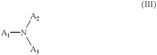
- the compound may have an asymmetric molecular structure as given by formula III:
- a 1 , A 2 and A 3 are each comprised of amino-substituted phenyl groups, which produce a hole transporting aryl amine functionality, with the proviso that A 1 is different from A 2 and A 3 .
- the phenyl groups of A 2 and A 3 may be joined so as to form a heterocyclic ring including the nitrogen, e.g., so as to constitute a carbazole group, or the phenyl groups of A 2 and A 3 may be unattached to each other.
- Each phenyl group may itself be fused with still another phenyl group and bonded to the nitrogen atom either, for example, as a 1-naphthyl group or as a 2-naphthyl group.
- the R- or A-groups of the compounds of formulas I, II or III may be charge carrier groups which, when present as a substituent in a material contained in a layer of an OLED, causes the material to provide electrical conduction through the layer, when a voltage is applied, preferentially by conduction of electrons, for example, an oxadiazole, a triazole, a thiophene or oligothiophene group.
- the present invention is, thus, directed to a glass for use in one or more of the charge carrier layers of an OLED, wherein the glass is comprised of a compound having an asymmetric molecular structure, the asymmetric molecules structure being comprised of a core atom or core chemical group that is bonded to at least two charge carrying substituents with at least one of the charge carrying substituents being different from the other substituent or, whenever there is more than one other charge carrying substituent, different from the other substituents.
- the compound having the asymmetric molecular structure may be the predominant component of the charge carrier layer or the asymmetric compound may be used as a dopant in the charge carrier layer.
- the present invention may typically be directed to compounds in which all the charge carrying substituents either have a hole transporting functionality or all substituents have an electron transporting functionality
- glasses containing hybrid compounds comprised of both types of charge carrying substituents also fall fully within the scope and spirit of the present invention, provided that such hybrid compounds do not have dipole moments which significantly inhibit carrier conduction by hindering charge carrier mobility.
- the present invention is, thus, further directed toward OLED layers comprised of such hybrid compounds.
- the separate emissive layer of a double heterostructure may be comprised of such a hybrid compound.
- the ⁇ - ⁇ -derivatives of NPD shown as the symmetric compounds S IX and S X in Table 2, respectively, were measured to have substantially the same T g values.
- T g values ranging from 54 to 125° C. Some of these materials have high T g values (e.g. compounds XI and XII), and may be useful as HTL materials by themselves.
- the thermal behavior for these asymmetric materials are all very similar, as illustrated in FIG. 2 for the sequence of DSC scans that were run for compound XII.
- On the first heating cycle after removing the sample from the sublimation tube in which it was prepared, only a melting transition is observed at 291° C. The sample is then cooled to room temperature and heated again.
- a T g is observed at 125° C. followed by a crystallization transition at 180° C. and a melt transition at the same temperature as before. If the sample is heated through the T g , but not the recrystallization transition the cycle can be repeated several times. If, however, the sample is heated through the recrystallization transition and then cooled, a T g is not observed on subsequent reheating.
- FIG. 2 shows the DSC scans for a mixture of compound I and CBP (10% compound I by weight). The sample in the DSC pan at this point was a solution of compound I in CBP. The sample was cooled from the melt and, on reheating, a T g of 107° C. and a recrystallization transition at 145° C.
- the thermal behavior for compounds I, IV, VI and VII all produced substantially the same thermal behavior, with substantially the same T g and recrystallization temperatures as observed for the mixtures shown in FIG. 2 .
- Mixtures were also examined with different ratios of the asymmetric HTL to CBP. Substantially the same thermal behavior was seen for these mixtures as was seen for the 10% mixture, i.e. a T g of 110-115° C. and recrystallization and melt transitions.
- OLEDs could be made from one of these mixtures by two different methods. In one case the materials could be deposited simultaneously from two sources, and in the other case a mixture could be prepared by evaporating a stable ratio or by spin coating a mixed solution.
- the OLEDs of the present invention are comprised of a heterostructure for producing electroluminescense which may be fabricated as a single heterostructure or as a double heterostructure.
- a heterostructure for producing electroluminescense which may be fabricated as a single heterostructure or as a double heterostructure.
- the materials, methods and apparatus for preparing the organic thin films of a single or double heterostructure are disclosed, for example, in U.S. Pat. No. 5,554,220, which is incorporated herein in its entirety by reference.
- the present invention is directed toward OLEDs which include a heterostructure for producing electroluminescense wherein the heterostructure includes at least one glassy charge carrier layer comprised of a compound having an asymmetric molecular structure.
- heterostructure for producing electroluminescense refers to a heterostructure that includes, for a single heterostructure, a substrate, a hole injecting anode layer in contact with the substrate, a hole transporting layer in contact with the anode layer, an electron transporting layer in contact with the hole transporting layer, and an electrode injecting cathode layer in contact with the hole electron transporting layer.
- the cathode layer is a metal cathode layer of Mg:Ag
- a metal protective layer for example, made of a layer of Ag for protecting the Mg:Ag cathode layer from atmospheric oxidation, may also be present.
- a double heterostructure is used to produce electroluminescense, a separate emissive layer is included between the hole transporting layer and the electron transporting layer.
- the OLED is comprised of a double heterostructure having an additional layer of emissive material between the hole transporting and electron transporting layers
- this additional layer is referred to as a “separate emissive layer” so as to distinguish it from the electron transporting layer of a single heterostructure that functions both as the electron transporting layer as well as the emissive layer that produces the electroluminescense.
- emissive layer as used herein, thus, may refer either to the emissive, electron transporting layer of a single heterostructure or the separate emissive layer of a double heterostructure.
- the heterostructure for producing electroluminescense may have an inverted (IOLED) structure in which the sequence of layers deposited on the substrate is inverted, that is, an electron injecting cathode layer is in direct contact with the substrate, an electron transporting layer is in contact with the cathode layer, a hole transporting layer is in contact with the electron transporting layer, and a hole injecting anode layer is in contact with the hole transporting layer.
- IOLED inverted
- the heterostructure for producing electroluminescense is included as part of a stacked OLED (SOLED)
- one or both of the electrodes of an individual heterostructure may be in contact with an electrode of an adjacent heterostructure.
- an insulating layer may be provided between adjacent electrodes of two of the OLEDs in the stack.
- a single heterostructure typically includes a substrate which may be opaque or transparent, rigid or flexible, and/or plastic, metal or glass; a first electrode, which is typically a high work function, hole-injecting anode layer, for example, an indium tin oxide (ITO) anode layer; a hole transporting layer; an electron transporting layer; and a second electrode layer, for example, a low work function, electron-injecting, metal cathode layer of a magnesium-silver alloy, (Mg:Ag) or of a lithium-aluminum alloy, (Li:Al).
- a substrate which may be opaque or transparent, rigid or flexible, and/or plastic, metal or glass
- a first electrode which is typically a high work function, hole-injecting anode layer, for example, an indium tin oxide (ITO) anode layer
- ITO indium tin oxide
- hole transporting layer for example, an electron transporting layer
- a second electrode layer for example, a low
- Materials that may be used as the substrate in a representative embodiment of the present invention include, in particular, glass, transparent polymer such as polyester, sapphire or quartz, or substantially any other material that may be used as the substrate of an OLED.
- Materials that may be used as the hole-injecting anode layer in a representative embodiment of the present invention include, in particular, ITO, Zn—In—SnO 2 or SbO 2 , or substantially any other material that may be used as the hole-injecting anode layer of an OLED.
- other materials that may be used in the hole transporting layer in a representative embodiment of the present invention include, in particular, N,N′-diphenyl-N,N′-bis(3-methylphenyl)1-1′biphenyl-4,4′diamine (TPD), 4,4′-bis[N-(1-naphthyl)-N-phenyl-amino]biphenyl ( ⁇ -NPD) or 4,4′-bis[N-(2-naphthyl)-N-phenyl-amino]biphenyl ( ⁇ -NPD).
- TPD N,N′-diphenyl-N,N′-bis(3-methylphenyl)1-1′biphenyl-4,4′diamine
- TPD N,N′-diphenyl-N,N′-bis(3-methylphenyl)1-1′biphenyl-4,4′diamine
- TPD N,N′-diphenyl-N,N
- Other materials that may be used as the electron transporting layer include, in particular, tris-(8-hydroxyquinoline)-aluminum (Alq 3 ) and carbazole.
- Other materials that may be used as the separate emissive layer, if present, include, in particular, dye-doped Alq 3 , or substantially any other material that may be used as the separate emissive layer of an OLED.
- Materials that may be used as the electron-injecting, metal cathode layer in a representative embodiment of the present invention include, in particular, Mg—Ag, Li—Ag or Ca, or substantially any other material that may be used as the cathode layer of an OLED.
- the insulating layer may be comprised of an insulating material such as SiO 2 , SiN x or AlO 2 , or substantially any other material that may be used as the insulating material of an OLED, which may be deposited by a variety of processes such as plasma enhanced chemical vapor deposition (PECVD), electron beam, etc.
- PECVD plasma enhanced chemical vapor deposition
- the OLEDs of the present invention have the advantage that they can be fabricated entirely from vacuum-deposited molecular organic materials as distinct, for example, from OLEDs in which some of the layers are comprised of polymeric materials, which cannot be readily deposited using vacuum deposition techniques.
- a vacuum-deposited material is one which can be deposited in a vacuum typically having a background pressure less than one atmosphere, preferably about 10 ⁇ 5 to about 10 ⁇ 11 torr for vacuum deposition, or about 50 torr to about 10 ⁇ 5 torr for vapor deposition.
- the substrate may be as thin as 10 ⁇ , if present as a flexible plastic or metal foil substrate, such as aluminum foil, or substantially thicker if present as a rigid, transparent or opaque, substrate or if the substrate is comprised of a silicon-based display driver;
- the present invention is directed to those devices in which the OLED is comprised of a heterostructure which includes at least one glassy charge carrier layer comprised of a compound having an asymmetric molecular structure.
- the present invention as disclosed herein may be used in conjunction with co-pending applications: “High Reliability, High Efficiency, Integratable Organic Light Emitting Devices and Methods of Producing Same”, Serial No. 08/774,119 (filed Dec. 23, 1996), now U.S. Pat. No. 6,046,543; “Novel Materials for Multicolor Light Emitting Diodes”, Ser. No. 08/850,264 (filed May 2, 1997), now U.S. Pat. No. 6,045,930; “Electron Transporting and Light Emitting Layers Based on Organic Free Radicals”, Ser. No. 08/774,120 (filed Dec. 23, 1996), now U.S. Pat. No. 5,811,833; “Multicolor Display Devices”, Ser. No.
- the materials that may be used as the substrate, the hole-injecting anode layer, the hole transporting layer, the electron transporting layer, the electron-injecting, metal cathode layer, the separate emissive layer if present, or the insulating layer, if present, include the materials as disclosed in these co-pending applications.
- the OLED of the present invention may be used in substantially any type of device which is comprised of an OLED, for example, in OLEDs that are incorporated into a larger display, a vehicle, a computer, a television, a printer, a large area wall, theater or stadium screen, a billboard or a sign.
- reaction mixture was precipitated by addition to 150 ml hexane. This solid was filtered, washed with hexane, and dried. The excess 4,4′-dibromobiphenyl was removed by sublimation at 150° C., leaving the product.
- Compound I was prepared as above except using the following amounts and using intermediate (1) for the halogenated aryl moiety. Reagents and amounts are, 3.104 mmol (0.681 g) 1-naphthyl-phenyl amine, 3.104 mmol (1.00 g) of intermediate (1), 0.0466 mmol (0.043 g) Pd 2 dba 3 , 0.0698 mmol (0.039 g) dppf, 4.66 mmol (0.522 g) sodium t-butoxide, and 15 ml toulene. Purification of the asymmetric products was as above except that the product itself was sublimed from the filtered solid.
- Compound II was prepared as above except using the following amounts and using intermediate (1) for the halogenated aryl moiety. Reagents and amounts are, 3,104 mmol (0.681 g) 2-naphthyl-phenyl amine, 3,104 mmol (1.00 g) of intermediate (1), 0.0466 mmol (0.043 g) Pd 2 dba 3 , 0.0698 mmol (0.039 g) dppf, 4.66 mmol (0.522 g) sodium t-butoxide, and 20 ml tolune. Purified as above.
- Compound III was prepared as above except using the following amounts and using intermediate (1) for the halogenated aryl moiety. Reagents and amounts are, 3,104 mmol (0.525 g) diphenyl amine, 3.104 mmol (1.00 g) of intermediate (1), 0.0466 mmol (0.043 g) Pd 2 dba 3 , 0.0698 Mmol (0.039 g) dppf, 4.66 (0.522 g) sodium t-butoxide, and 20 ml toluene. Purified as above.
- Compound IV was prepared as above except using the following amounts and using intermediate (1) for the halogenated aryl moiety. Reagents and amounts are, 3,104 mmol (0.509 g) phenyl-o-tolyl amine, mine, 3.104 mmol (1.00 g) of intermediate (1), 0.0466 mmol (0.043 g) Pd 2 dba 3 , 0.0698 mmol (0.039 g) dppf, 4.66 mmol (0.522 g) sodium t-butoxide, and 20 ml toluene. Purified as above.
- Compound V was prepared as above except using the following amounts and using intermediate (1) for the halogenated aryl moiety. Reagents and amounts are, 3.104 mmol (0.606 g) iminodibenzyl, 3.104 mmol (1.00 g) of intermediate (1), 0.0466 mmol (0.043 g) Pd 2 dba 3 , 0.0698 mmol (0.039 g) dppf, 4.66 mmol (0.522 g) sodium t-butoxide, and 20 ml toluene. Purified as above.
- Compound VI was prepared as above except using the following amounts and using intermediate (1) for the halogenated aryl moiety. Reagents and amounts are, 3.104 mmol (0.600 g) iminostilbene, 3.104 mmol (1.00 g) of intermediate (1), 0.0466 mmol (0.043 g) Pd 2 dba 3 , 0.0698 mmol (0.039 g) dppf, 4.66 mmol (0.522 g) sodium t-butoxide, and 20 ml toluene. Purified as above.
- Compound VII was prepared as above except using the following amounts and using intermediate (2) for the halogenated aryl moiety. Reagents and amounts are, 1.26 mmol (0.275 g) 1-naphthyl-phenyl amine, 1.26 mmol (0.500 g) of intermediate (2), 0.0189 mmol (0.017 g) Pd 2 dba 3 , 0.0284 mmol (0.016 g) dppf, 1.89 mmol (0.182 g) sodium t-butoxide, and 15 ml toluene. Purified as above.
- Compound IX was prepared as above except using the following amounts and using intermediate (2) for the halogenated aryl moiety. Reagents and amounts are, 0.992 mmol (0.162 g) diphenyl amine, 0.992 mmol (0.395 g) of intermediate (2), 0.0149 mmol (0.014 g) Pd 2 dba 3 , 0.0223 mmol (0.012 g) dppf, 1.49 mmol (0.143 g) sodium t-butoxide, and 15 ml toluene. Purified as above.
- Compound X was prepared as above except using the following amounts and using intermediate (2) for the halogenated aryl moiety. Reagents and amounts are, 1.26 mmol (0.230 g) phenyl-o-tolyl amine, 1.26 mmol (0.500 g) of intermediate (2), 0.0189 mmol (0.017 g) Pd 2 dba 3 , 0.0284 mmol (0.016 g) dppf, 1.89 mmol (0.182 g) sodium t-butoxide, and 15 ml toluene. Purified as above.
- Compound XI was prepared as above except using the following amounts and using intermediate (2) for the halogenated aryl moiety. Reagents and amounts are, 0.934 mmol (0.182 g) iminodibenzyl, 0.934 mmol (0.367 g) of intermediate (2), 0.0141 mmol (0.013 g) Pd 2 dba 3 , 0.0234 mmol (0.012 g) dppf, 1.40 mmol (0.135 g) sodium t-butoxide, and 10 ml toluene. Purified as above.
- Compound XII was prepared as above except using the following amounts and using intermediate (2) for the halogenated aryl moiety. Reagents and amounts are, 0.928 mmol (0.180 g) iminostilbene, 0.928 mmol (0.370 g) of intermediate (2), 0.0141 mmol (0.013 g) Pd 2 dba 3 , 0.0234 mmol (0.012 g) dppf, 1.39 mmol (0.134 g) sodium t-butoxide, and 10 ml toluene. Purified as above.
- the hole transporting material compound VII was prepared, as described above, by Ullman coupling, and the electron transporting material Alq 3 was synthesized according to literature procedure. All materials were sublimed before use.
- the ITO/Borosilicate substrates (100 ⁇ /square) were cleaned by sonicating with detergent for five minutes followed by rinsing with deionized water. They were then treated twice in boiling 1,1,1-trichloroethane for two minutes. The substrates were then sonicated twice with acetone for two minutes and twice with methanol for two minutes.
- the background pressure prior to deposition was 8 ⁇ 10 ⁇ 7 torr and the pressure during the deposition was around 5 ⁇ 10 ⁇ 7 to 2 ⁇ 10 ⁇ 6 torr.
- the chemicals were sublimed from resistively heated tantalum boats, and then deposited at a rate from 1 to 3.6 ⁇ /s.
- the thickness was controlled at 300 ⁇ .
- the electron transporting layer (Alq 3 ) was deposited at a rate between 1 to 3.3 ⁇ /s. The total thickness of this layer was controlled at 450 ⁇ .
- the substrates were then released to air and masks were put directly on the substrates.
- the masks are made of stainless steel sheet and contain holes with diameters of 0.25, 0.5, 0.75, and 1.0 mm.
- the substrates were then put back into vacuum for further coating.
- Magnesium and silver were co-deposited at a rate of 2 ⁇ /s.
- the ratio of Mg:Ag was 9:1.
- the thickness of this layer was 500 ⁇ .
- 1000 ⁇ Ag was deposited at the rate of 2.7 ⁇ /s.
- the devices were characterized within three hours of fabrication. Electroluminescent spectra, I-V curves, and quantum yields from direct front were measured. The electroluminescent spectrum for the device is shown in FIG. 3 and the current-voltage (I-V) characteristics are shown in FIG. 4 . The external quantum yield was measured to be substantially identical to that of a standard Alq 3 /TPD device made at the same time under substantially the same conditions. These results show that this class of asymmetric compounds can function as hole transporting materials in OLEDs.
Abstract

Description


| TABLE 1 |
| Compounds having the single phenylene core of formula I. |
| R4 = |
| R1 = |
 |
 |
 |
 |
 |
Mp = 310° C. Tg = NA S I | Mp = 215° C. Tg = 88° C. I | Mp = 212° C. Tg = 83° C. II | Mp = 158° C. Tg = 61° III |
 |
Mp = 185° C. Tg = 70° C. S II | |||
 |
Mp = 184° C. Tg = 70° C. S III | |||
 |
||||
 |
||||
 |
||||
 |
||||
| R4 = |
| R1 = |
 |
 |
 |
 |
Mp = 139° C. Tg = 54° C. IV | Mp = 233° C. Tg = 91° C. V | Mp = 259° C. Tg = 103° C. VI |
 |
|||
 |
|||
 |
|||
 |
|||
 |
|||
 |
|||
| TABLE 2 |
| Compounds having the biphenylene core of formula II |
| R6 = |
| R1 = |
 |
 |
 |
 |
 |
Mp = 290° C. Tg = NA S VIII | Mp = 253° C. Tg = 109° C. VII | Mp = 249° C. Tg = 107° C. VIII | Mp = 217° C. Tg = 91° IX |
 |
Mp = 265° C. Tg = 100° C. S IX | |||
 |
Mp = 266° C. Tg = 101° C. S X | |||
 |
||||
 |
||||
 |
||||
 |
||||
| R6 = |
| R1 = |
 |
 |
 |
 |
Mp = 198° C. Tg = 85° C. X | Mp = 273° C. Tg = 117° C. XI | Mp = 291° C. Tg = 125° C. XII |
 |
|||
 |
|||
 |
|||
 |
Mp = 175° C. Tg = 60° C. S XII | ||
 |
|||
 |
|||
Claims (13)


Priority Applications (4)
| Application Number | Priority Date | Filing Date | Title |
|---|---|---|---|
| US08/925,029 US6242115B1 (en) | 1997-09-08 | 1997-09-08 | OLEDs containing thermally stable asymmetric charge carrier materials |
| AU92202/98A AU9220298A (en) | 1997-09-08 | 1998-09-04 | Oleds containing thermally stable asymmetric charge carrier materials |
| TW87114720A TW469750B (en) | 1997-09-08 | 1998-09-04 | OLEDS containing thermally stable asymmetric charge carrier materials |
| PCT/US1998/018363 WO1999013691A1 (en) | 1997-09-08 | 1998-09-04 | Oleds containing thermally stable asymmetric charge carrier materials |
Applications Claiming Priority (1)
| Application Number | Priority Date | Filing Date | Title |
|---|---|---|---|
| US08/925,029 US6242115B1 (en) | 1997-09-08 | 1997-09-08 | OLEDs containing thermally stable asymmetric charge carrier materials |
Publications (1)
| Publication Number | Publication Date |
|---|---|
| US6242115B1 true US6242115B1 (en) | 2001-06-05 |
Family
ID=25451095
Family Applications (1)
| Application Number | Title | Priority Date | Filing Date |
|---|---|---|---|
| US08/925,029 Expired - Lifetime US6242115B1 (en) | 1997-09-08 | 1997-09-08 | OLEDs containing thermally stable asymmetric charge carrier materials |
Country Status (4)
| Country | Link |
|---|---|
| US (1) | US6242115B1 (en) |
| AU (1) | AU9220298A (en) |
| TW (1) | TW469750B (en) |
| WO (1) | WO1999013691A1 (en) |
Cited By (105)
| Publication number | Priority date | Publication date | Assignee | Title |
|---|---|---|---|---|
| US6387544B1 (en) * | 1998-04-10 | 2002-05-14 | The Trustees Of Princeton University | OLEDS containing thermally stable glassy organic hole transporting materials |
| US6436558B1 (en) * | 1998-08-07 | 2002-08-20 | Fuji Photo Film Co., Ltd. | Organic electroluminescence element |
| US20030022020A1 (en) * | 2001-07-27 | 2003-01-30 | The Ohio State University | Methods for producing electroluminescent devices by screen printing |
| US6558736B2 (en) | 1997-11-17 | 2003-05-06 | The Trustees Of Princeton University | Low pressure vapor phase deposition of organic thin films |
| US20030124265A1 (en) * | 2001-12-04 | 2003-07-03 | 3M Innovative Properties Company | Method and materials for transferring a material onto a plasma treated surface according to a pattern |
| US6602790B2 (en) | 2001-02-14 | 2003-08-05 | Avery Dennison Corporation | Method for patterning a multilayered conductor/substrate structure |
| US20030203236A1 (en) * | 1997-12-01 | 2003-10-30 | Thompson Mark E. | OLEDs doped with phosphorescent compounds |
| US20030205696A1 (en) * | 2002-04-25 | 2003-11-06 | Canon Kabushiki Kaisha | Carbazole-based materials for guest-host electroluminescent systems |
| US6645645B1 (en) * | 2000-05-30 | 2003-11-11 | The Trustees Of Princeton University | Phosphorescent organic light emitting devices |
| US20030219625A1 (en) * | 2002-04-19 | 2003-11-27 | 3M Innovative Properties Company | Materials for organic electronic devices |
| US20030224205A1 (en) * | 2002-04-19 | 2003-12-04 | 3M Innovative Properties Company | Electroluminescent materials and methods of manufacture and use |
| US20040001915A1 (en) * | 2002-06-14 | 2004-01-01 | Avery Dennison Corporation | Method for roll-to-roll deposition of optically transparent and high conductivity metallic thin films |
| US20040004433A1 (en) * | 2002-06-26 | 2004-01-08 | 3M Innovative Properties Company | Buffer layers for organic electroluminescent devices and methods of manufacture and use |
| US6699597B2 (en) | 2001-08-16 | 2004-03-02 | 3M Innovative Properties Company | Method and materials for patterning of an amorphous, non-polymeric, organic matrix with electrically active material disposed therein |
| US20040119403A1 (en) * | 2002-12-19 | 2004-06-24 | 3M Innovative Properties Company | Organic electroluminescent device and encapsulation method |
| US20040151943A1 (en) * | 2003-02-04 | 2004-08-05 | Shuit-Tong Lee | Electroluminescent devices |
| US20040214036A1 (en) * | 2003-04-15 | 2004-10-28 | 3M Innovative Properties Company | Electron transport agents for organic electronic devices |
| US20040214037A1 (en) * | 2003-04-15 | 2004-10-28 | Roberts Ralph R. | Ethynyl containing electron transport dyes and compositions |
| US6830828B2 (en) | 1998-09-14 | 2004-12-14 | The Trustees Of Princeton University | Organometallic complexes as phosphorescent emitters in organic LEDs |
| EP1489155A1 (en) * | 2002-03-22 | 2004-12-22 | Idemitsu Kosan Co., Ltd. | Material for organic electroluminescent devices and organic electroluminescent devices made by using the same |
| US20040262576A1 (en) * | 1999-03-23 | 2004-12-30 | Thompson Mark E. | Organometallic complexes as phosphorescent emitters in organic LEDs |
| US20050116621A1 (en) * | 2003-11-18 | 2005-06-02 | Erika Bellmann | Electroluminescent devices and methods of making electroluminescent devices including a color conversion element |
| US20050118923A1 (en) * | 2003-11-18 | 2005-06-02 | Erika Bellmann | Method of making an electroluminescent device including a color filter |
| US20050154234A1 (en) * | 2003-12-03 | 2005-07-14 | Orient Chemical Ind., Ltd. | Triarylamine dimer derivative having amorphous phase |
| US20060008577A1 (en) * | 2001-08-16 | 2006-01-12 | 3M Innovative Properties Company | Method and materials for patterning of a polymerizable, amorphous matrix with electrically active material disposed therein |
| KR100556422B1 (en) | 2004-04-19 | 2006-03-03 | 엘지전자 주식회사 | organic electroluminescence device for blue phosphorescence |
| US20060082291A1 (en) * | 2004-08-23 | 2006-04-20 | Lg Chem, Ltd. | Luminescent material and organic electroluminescent device using the same |
| US20060105199A1 (en) * | 2004-11-18 | 2006-05-18 | 3M Innovative Properties Company | Electroluminescent devices containing trans-1,2-bis(acenyl)ethylene compounds |
| US20060102893A1 (en) * | 2004-11-18 | 2006-05-18 | 3M Innovative Properties Company | Semiconductors containing trans-1,2-bis(acenyl)ethylene compoounds |
| US20060131505A1 (en) * | 2004-12-17 | 2006-06-22 | Eastman Kodak Company | Imaging element |
| US20060131504A1 (en) * | 2004-12-17 | 2006-06-22 | Eastman Kodak Company | Display |
| US20060131393A1 (en) * | 2004-12-22 | 2006-06-22 | Eastman Kodak Company | Multi-role transaction card |
| US20060136997A1 (en) * | 2004-12-21 | 2006-06-22 | Eastman Kodak Company | Authentication system and method |
| US20060132477A1 (en) * | 2004-12-17 | 2006-06-22 | Eastman Kodak Company | Methods for making display |
| US20060136734A1 (en) * | 2004-12-21 | 2006-06-22 | Eastman Kodak Company | Identification display device |
| US20060142520A1 (en) * | 2004-12-27 | 2006-06-29 | 3M Innovative Properties Company | Hole transport layers for organic electroluminescent devices |
| US20060138945A1 (en) * | 2004-12-28 | 2006-06-29 | Wolk Martin B | Electroluminescent devices and methods of making electroluminescent devices including an optical spacer |
| US20060181658A1 (en) * | 2005-02-16 | 2006-08-17 | Eastman Kodak Company | Conductive absorption layer for flexible displays |
| US20060228974A1 (en) * | 2005-03-31 | 2006-10-12 | Theiss Steven D | Methods of making displays |
| US20060263631A1 (en) * | 2004-11-05 | 2006-11-23 | Samsung Sdi Co., Ltd. | Organic light-emitting device |
| US20070001927A1 (en) * | 2005-07-01 | 2007-01-04 | Eastman Kodak Company | Tiled display for electronic signage |
| US20070036887A1 (en) * | 2005-08-11 | 2007-02-15 | 3M Innovative Properties Company | Method for making a thin film layer |
| US20070085838A1 (en) * | 2005-10-17 | 2007-04-19 | Ricks Theodore K | Method for making a display with integrated touchscreen |
| WO2007058044A1 (en) | 2005-11-15 | 2007-05-24 | Idemitsu Kosan Co., Ltd. | Aromatic amine derivative and organic electroluminescent element employing the same |
| WO2007058127A1 (en) | 2005-11-16 | 2007-05-24 | Idemitsu Kosan Co., Ltd. | Aromatic amine derivative and organic electroluminescent element using the same |
| US20070145888A1 (en) * | 2005-11-16 | 2007-06-28 | Idemitsu Kosan Co., Ltd. | Aromatic amine derivatives and organic electroluminescence device using the same |
| WO2007080704A1 (en) | 2006-01-13 | 2007-07-19 | Idemitsu Kosan Co., Ltd. | Aromatic amine derivatives and organic electroluminescent devices made by using the same |
| US20070185386A1 (en) * | 2006-02-07 | 2007-08-09 | Eric Cheng | Medical device light source |
| EP1840120A1 (en) | 2006-03-27 | 2007-10-03 | Novaled AG | N-Heterocyclic compounds and their use in electronic, optoelectronic and electroluminiscent components |
| WO2007125714A1 (en) | 2006-04-26 | 2007-11-08 | Idemitsu Kosan Co., Ltd. | Aromatic amine derivative, and organic electroluminescence element using the same |
| WO2007148660A1 (en) | 2006-06-22 | 2007-12-27 | Idemitsu Kosan Co., Ltd. | Organic electroluminescent device employing heterocycle-containing arylamine derivative |
| WO2008001551A1 (en) | 2006-06-27 | 2008-01-03 | Idemitsu Kosan Co., Ltd. | Aromatic amine derivative, and organic electroluminescence device using the same |
| WO2008023549A1 (en) | 2006-08-23 | 2008-02-28 | Idemitsu Kosan Co., Ltd. | Aromatic amine derivatives and organic electroluminescent devices made by using the same |
| US20080102310A1 (en) * | 2006-10-27 | 2008-05-01 | Thompson Mark E | Materials and architectures for efficient harvesting of singlet and triplet excitons for white light emitting OLEDs |
| WO2008062636A1 (en) | 2006-11-24 | 2008-05-29 | Idemitsu Kosan Co., Ltd. | Aromatic amine derivative and organic electroluminescent element using the same |
| US20080124455A1 (en) * | 2006-11-24 | 2008-05-29 | Samsung Electronics Co., Ltd. | Organic light emitting compound, organic light emitting device comprising the same, and method of manufacturing the organic light emitting device |
| US20080254318A1 (en) * | 2004-12-28 | 2008-10-16 | Semiconductor Energy Laboratory Co., Ltd. | Carbazole Derivative, and Light-Emitting Element and Light-Emitting Device Using the Carbzole Derivative |
| US20090012367A1 (en) * | 2003-12-17 | 2009-01-08 | Boston Scientific Scimed, Inc. | Medical device with oled illumination light source |
| WO2009020095A1 (en) | 2007-08-06 | 2009-02-12 | Idemitsu Kosan Co., Ltd. | Aromatic amine derivative and organic electroluminescent device using the same |
| US20090087061A1 (en) * | 2007-09-27 | 2009-04-02 | Siemens Medical Solutions Usa, Inc. | Intrinsic Co-Registration For Modular Multimodality Medical Imaging Systems |
| US20090155458A1 (en) * | 2006-02-08 | 2009-06-18 | Roehrig Mark A | Method for manufacturing on a film substrate at a temperature above its glass transition |
| WO2009081857A1 (en) | 2007-12-21 | 2009-07-02 | Idemitsu Kosan Co., Ltd. | Organic electroluminescent device |
| US20100020039A1 (en) * | 2005-10-17 | 2010-01-28 | Industrial Technology Research Institute | Touch input device with display front |
| US20100084645A1 (en) * | 2005-03-23 | 2010-04-08 | Semiconductor Energy Laboratory Co., Ltd. | Composite material, and light emitting element and light emitting device using the composite material |
| WO2010044130A1 (en) | 2008-10-17 | 2010-04-22 | 三井化学株式会社 | Aromatic amine derivative and organic electroluminescent device using the same |
| WO2010061824A1 (en) | 2008-11-25 | 2010-06-03 | 出光興産株式会社 | Aromatic amine derivative, and organic electroluminescent element |
| DE102008061843A1 (en) | 2008-12-15 | 2010-06-17 | Novaled Ag | Heterocyclic compounds and their use in electronic and optoelectronic devices |
| US20110163660A1 (en) * | 2000-03-27 | 2011-07-07 | Idemitsu Kosan Co., Ltd. | Organic electroluminescence element |
| WO2011090149A1 (en) | 2010-01-21 | 2011-07-28 | 出光興産株式会社 | Aromatic amine derivative, and organic electroluminescent element comprising same |
| EP2371810A1 (en) | 2005-01-05 | 2011-10-05 | Idemitsu Kosan Co., Ltd. | Aromatic amine derivative and organic electroluminescent device using same |
| EP2423179A1 (en) * | 2009-04-24 | 2012-02-29 | Idemitsu Kosan Co., Ltd. | Aromatic amine derivative and organic electroluminescent element comprising same |
| USRE44071E1 (en) | 2001-02-14 | 2013-03-12 | Streaming Sales Llc | Method for patterning a multilayered conductor/substrate structure |
| CN103262284A (en) * | 2010-12-13 | 2013-08-21 | 欧司朗光电半导体有限公司 | Optoelectronic component, and use of a copper complex in a charge generation layer sequence |
| US20130270524A1 (en) * | 2012-04-17 | 2013-10-17 | Samsung Display Co. Ltd. | Compound for organic light-emitting diode and organic light-emitting diode including the same |
| US20140231713A1 (en) * | 2011-09-28 | 2014-08-21 | Solvay Sa | Spirobifluorene compounds for light emitting devices |
| KR20140145964A (en) | 2013-02-14 | 2014-12-24 | 덕산하이메탈(주) | Compound for organic electronic element, organic electronic element using the same, and an electronic device thereof |
| US20150014657A1 (en) * | 2013-07-15 | 2015-01-15 | Samsung Display Co., Ltd. | Organic light emitting device |
| US8950328B1 (en) | 2004-12-29 | 2015-02-10 | E I Du Pont De Nemours And Company | Methods of fabricating organic electronic devices |
| KR101493482B1 (en) | 2014-08-29 | 2015-02-16 | 덕산네오룩스 주식회사 | Organic electronic element using a compound for organic electronic element, and an electronic device thereo |
| US20150212450A1 (en) * | 2012-08-07 | 2015-07-30 | Canon Kabushiki Kaisha | Novel fused polycyclic compound and organic light-emitting device, display apparatus, image information processing apparatus, lighting system, and image forming apparatus having the compound |
| KR20150089427A (en) | 2014-01-28 | 2015-08-05 | 덕산네오룩스 주식회사 | Compound for organic electronic element, organic electronic element using the same, and an electronic device thereof |
| US20150333272A1 (en) * | 2012-05-31 | 2015-11-19 | Konica Minolta, Inc. | Transparent electrode, electronic device, and organic electroluminescent element |
| US20150364696A1 (en) * | 2014-06-13 | 2015-12-17 | Samsung Display Co., Ltd. | Organic light-emitting device and method of manufacturing the same |
| US9252370B2 (en) | 2012-11-05 | 2016-02-02 | Samsung Display Co., Ltd. | Heterocyclic compounds and organic light emitting devices including the same |
| US9385325B2 (en) | 2012-11-05 | 2016-07-05 | Samsung Display Co., Ltd. | Heterocyclic compound and organic light emitting device including the same |
| US9444053B2 (en) | 2006-04-26 | 2016-09-13 | Idemitsu Kosan Co., Ltd. | Aromatic amine derivative and electroluminescence device using the same |
| US9913573B2 (en) | 2003-04-01 | 2018-03-13 | Boston Scientific Scimed, Inc. | Endoscopic imaging system |
| US10043980B2 (en) | 2015-03-30 | 2018-08-07 | Samsung Display Co., Ltd. | Compound and organic light-emitting device including the same |
| US10217944B2 (en) | 2014-01-22 | 2019-02-26 | Duk San Neolux Co., Ltd. | Compound for organic electronic element, organic electronic element using the same, and an electronic device thereof |
| US20190326520A1 (en) * | 2018-04-24 | 2019-10-24 | Samsung Display Co., Ltd. | Organic light-emitting device and method of manufacturing the same |
| US10937967B2 (en) | 2017-10-12 | 2021-03-02 | Samsung Display Co., Ltd. | Amine-based compound and organic light-emitting device including the amine-based compound |
| US11289657B2 (en) | 2018-03-26 | 2022-03-29 | Samsung Display Co., Ltd. | Heterocyclic compound and organic light-emitting device including the same |
| US11437585B2 (en) | 2019-02-13 | 2022-09-06 | Samsung Display Co., Ltd. | Organic light-emitting device |
| US11444247B2 (en) | 2019-10-08 | 2022-09-13 | Samsung Display Co., Ltd. | Compound and organic light-emitting device including the same |
| US11440902B2 (en) | 2018-06-08 | 2022-09-13 | Samsung Display Co., Ltd. | Amine-based compound and organic light-emitting device including the same |
| US11450811B2 (en) | 2018-08-10 | 2022-09-20 | Samsung Display Co., Ltd. | Condensed cyclic compound and organic light-emitting device including the same |
| US11594684B2 (en) | 2019-09-27 | 2023-02-28 | Samsung Display Co., Ltd. | Condensed-cyclic compound and organic light emitting device including the same |
| US11600781B2 (en) | 2019-03-21 | 2023-03-07 | Samsung Display Co., Ltd. | Organic electroluminescence device and monoamine compound for organic electroluminescence device |
| US11711978B2 (en) | 2019-09-16 | 2023-07-25 | Samsung Display Co., Ltd. | Heterocyclic compound and organic light-emitting device including the same |
| US11744147B2 (en) | 2020-01-21 | 2023-08-29 | Samsung Display Co., Ltd. | Light emitting diode and display device including the same |
| US11770973B2 (en) | 2019-06-19 | 2023-09-26 | Samsung Display Co., Ltd. | Organic electroluminescence device and amine compound for organic electroluminescence device |
| US11805697B2 (en) | 2018-01-26 | 2023-10-31 | Samsung Display Co., Ltd. | Organic electroluminescence device and monoamine compound for organic electroluminescence device |
| US11849632B2 (en) | 2019-03-20 | 2023-12-19 | Samsung Display Co., Ltd. | Amine-based compound and organic light-emitting device including the same |
| US11871656B2 (en) | 2018-01-26 | 2024-01-09 | Samsung Display Co., Ltd. | Organic electroluminescence device and monoamine compound for organic electroluminescence device |
| US11910705B2 (en) * | 2018-02-02 | 2024-02-20 | Duk San Neolux Co., Ltd. | Compound for organic electric element, organic electric element using the same, and electronic device thereof |
Families Citing this family (10)
| Publication number | Priority date | Publication date | Assignee | Title |
|---|---|---|---|---|
| JP4573923B2 (en) * | 1999-04-27 | 2010-11-04 | 三井化学株式会社 | Amine compounds |
| WO2001056091A2 (en) * | 2000-01-28 | 2001-08-02 | Siemens Aktiengesellschaft | Charge transport material having an increased glass transition temperature and the use of said material |
| KR20010044090A (en) * | 2000-09-06 | 2001-06-05 | 박종욱 | A compound for electrolumines cene display containing carbazol and stilbene, and the high efficiency electroluminescene display using thereof |
| CN100335462C (en) * | 2003-09-05 | 2007-09-05 | 清华大学 | Carbazole derivative and its application in electroluminescent device |
| JP4587703B2 (en) * | 2004-05-07 | 2010-11-24 | ケミプロ化成株式会社 | Novel quarter phenylene derivative and organic EL device using the same |
| JP2008120769A (en) * | 2006-11-15 | 2008-05-29 | Bando Chem Ind Ltd | New aromatic tertiary amines and utilization thereof |
| US9349964B2 (en) | 2010-12-24 | 2016-05-24 | Lg Chem, Ltd. | Organic light emitting diode and manufacturing method thereof |
| JP5798754B2 (en) * | 2011-02-14 | 2015-10-21 | ケミプロ化成株式会社 | Novel substituted diphenylcarbazole derivative, host material comprising the derivative, and organic electroluminescence device comprising the derivative |
| EP2746361B1 (en) * | 2011-12-23 | 2016-08-17 | LG Chem, Ltd. | Organic light-emitting diode |
| KR101745109B1 (en) | 2014-08-20 | 2017-06-09 | 주식회사 엘지화학 | Organic light emitting diode |
Citations (11)
| Publication number | Priority date | Publication date | Assignee | Title |
|---|---|---|---|---|
| US5061569A (en) | 1990-07-26 | 1991-10-29 | Eastman Kodak Company | Electroluminescent device with organic electroluminescent medium |
| JPH04288369A (en) * | 1991-03-18 | 1992-10-13 | Minolta Camera Co Ltd | New hydrazone compound and photoreceptor prepared by using same |
| US5281489A (en) * | 1990-03-16 | 1994-01-25 | Asashi Kasei Kogyo Kabushiki Kaisha | Electroluminescent element |
| US5378519A (en) * | 1992-04-28 | 1995-01-03 | Canon Kabushiki Kaisha | Electroluminescent device |
| US5512400A (en) * | 1993-12-15 | 1996-04-30 | Hodogaya Chemical Co., Ltd. | Hydrazone compound and electrophotographic photoreceptor and organic electroluminescent element both containing the same |
| US5702833A (en) * | 1995-03-08 | 1997-12-30 | Ricoh Company, Ltd. | Organic electroluminescent element |
| US5747205A (en) * | 1997-02-27 | 1998-05-05 | Xerox Corporation | Photoconductive imaging members |
| US5792557A (en) * | 1994-02-08 | 1998-08-11 | Tdk Corporation | Organic EL element |
| US5792567A (en) * | 1994-03-16 | 1998-08-11 | Sumitomo Electric Industries, Ltd. | Triazole derivatives and organic electroluminescent devices produced therefrom |
| US5811833A (en) | 1996-12-23 | 1998-09-22 | University Of So. Ca | Electron transporting and light emitting layers based on organic free radicals |
| US5968675A (en) * | 1995-12-11 | 1999-10-19 | Toyo Ink Manufacturing Co., Ltd. | Hole-transporting material and use thereof |
-
1997
- 1997-09-08 US US08/925,029 patent/US6242115B1/en not_active Expired - Lifetime
-
1998
- 1998-09-04 AU AU92202/98A patent/AU9220298A/en not_active Abandoned
- 1998-09-04 TW TW87114720A patent/TW469750B/en not_active IP Right Cessation
- 1998-09-04 WO PCT/US1998/018363 patent/WO1999013691A1/en active Application Filing
Patent Citations (11)
| Publication number | Priority date | Publication date | Assignee | Title |
|---|---|---|---|---|
| US5281489A (en) * | 1990-03-16 | 1994-01-25 | Asashi Kasei Kogyo Kabushiki Kaisha | Electroluminescent element |
| US5061569A (en) | 1990-07-26 | 1991-10-29 | Eastman Kodak Company | Electroluminescent device with organic electroluminescent medium |
| JPH04288369A (en) * | 1991-03-18 | 1992-10-13 | Minolta Camera Co Ltd | New hydrazone compound and photoreceptor prepared by using same |
| US5378519A (en) * | 1992-04-28 | 1995-01-03 | Canon Kabushiki Kaisha | Electroluminescent device |
| US5512400A (en) * | 1993-12-15 | 1996-04-30 | Hodogaya Chemical Co., Ltd. | Hydrazone compound and electrophotographic photoreceptor and organic electroluminescent element both containing the same |
| US5792557A (en) * | 1994-02-08 | 1998-08-11 | Tdk Corporation | Organic EL element |
| US5792567A (en) * | 1994-03-16 | 1998-08-11 | Sumitomo Electric Industries, Ltd. | Triazole derivatives and organic electroluminescent devices produced therefrom |
| US5702833A (en) * | 1995-03-08 | 1997-12-30 | Ricoh Company, Ltd. | Organic electroluminescent element |
| US5968675A (en) * | 1995-12-11 | 1999-10-19 | Toyo Ink Manufacturing Co., Ltd. | Hole-transporting material and use thereof |
| US5811833A (en) | 1996-12-23 | 1998-09-22 | University Of So. Ca | Electron transporting and light emitting layers based on organic free radicals |
| US5747205A (en) * | 1997-02-27 | 1998-05-05 | Xerox Corporation | Photoconductive imaging members |
Non-Patent Citations (7)
| Title |
|---|
| E. Han, L. Do, M. Fujihara, H. Inada and Y. Shirota, J. Appl. Phys., vol. 80 (Sep. 1996), pp. 3297-3305. |
| K. Naito and A. Miura, J. Phys. Chem., vol. 97 (1993), pp. 6240-6248, (no month). |
| S. Tokito, H. Tanaka, A. Okada and Y. Taga, Appl. Phys. Lett., vol. 69, No. 7 (Aug. 1996), pp. 878-880. |
| S. Van Slyke, C. Chen and C. Tang, Appl. Phys. Lett., vol. 69, No. 15 (Oct. 1996), pp. 2160-2162. |
| T. Noda, H. Ogawa, N. Noma Y. Shirota, Appl. Phys. Lett., vol. 70, No. 6, (Feb. 1997), pp. 699-701. |
| T. Noda, I. Imae, N. Noma and Y. Shirota, Advance Materials, vol. 9, No. 3, (1997), pp. 239-241, (no month). |
| Y. Shirota, T. Kobata and N. Noma, Chem. Lett. (1989), pp. 1145-1148, (no month). |
Cited By (233)
| Publication number | Priority date | Publication date | Assignee | Title |
|---|---|---|---|---|
| US20100104753A1 (en) * | 1997-11-17 | 2010-04-29 | Forrest Stephen R | Low pressure vapor phase deposition of organic thin films |
| US20040007178A1 (en) * | 1997-11-17 | 2004-01-15 | Forrest Stephen R. | Low pressure vapor phase deposition of organic thin films |
| US20070131172A1 (en) * | 1997-11-17 | 2007-06-14 | Forrest Stephen R | Low pressure vapor phase deposition of organic thin films |
| US6558736B2 (en) | 1997-11-17 | 2003-05-06 | The Trustees Of Princeton University | Low pressure vapor phase deposition of organic thin films |
| US20150114296A1 (en) * | 1997-11-17 | 2015-04-30 | The Trustees Of Princeton University | Low pressure vapor phase deposition of organic thin films |
| US7488542B2 (en) | 1997-12-01 | 2009-02-10 | The Trustees Of Princeton University | OLEDs doped with phosphorescent compounds |
| US20110147727A1 (en) * | 1997-12-01 | 2011-06-23 | Thompson Mark E | Oleds doped with phosphorescent compounds |
| US7279237B2 (en) | 1997-12-01 | 2007-10-09 | The Trustees Of Princeton University | OLEDs doped with phosphorescent compounds |
| US7279235B2 (en) | 1997-12-01 | 2007-10-09 | The Trustees Of Princeton University | OLEDs doped with phosphorescent compounds |
| US20060286409A1 (en) * | 1997-12-01 | 2006-12-21 | Thompson Mark E | OLEDs doped with phosphorescent compounds |
| US20080024058A1 (en) * | 1997-12-01 | 2008-01-31 | Thompson Mark E | OLEDs doped with phosphorescent compounds |
| US9508940B2 (en) | 1997-12-01 | 2016-11-29 | The Trustees Of Princeton University | OLEDs doped with phosphorescent compounds |
| US20050008897A1 (en) * | 1997-12-01 | 2005-01-13 | Thompson Mark E. | OLEDs doped with phosphorescent compounds |
| US6872477B2 (en) | 1997-12-01 | 2005-03-29 | The Trustees Of Princeton University | OLEDs doped with phosphorescent compounds |
| US20030203236A1 (en) * | 1997-12-01 | 2003-10-30 | Thompson Mark E. | OLEDs doped with phosphorescent compounds |
| US20050214570A1 (en) * | 1997-12-01 | 2005-09-29 | Thompson Mark E | OLEDs doped with phosphorescent compounds |
| US20050158584A1 (en) * | 1997-12-01 | 2005-07-21 | Thompson Mark E. | OLEDs doped with phosphorescent compounds |
| US7901795B2 (en) | 1997-12-01 | 2011-03-08 | The Trustees Of Princeton University | OLEDs doped with phosphorescent compounds |
| US7563519B2 (en) | 1997-12-01 | 2009-07-21 | The Trustees of Frinceton University | OLEDs doped with phosphorescent compounds |
| US20090256476A1 (en) * | 1997-12-01 | 2009-10-15 | Thompson Mark E | Oleds doped with phosphorescent compounds |
| US6387544B1 (en) * | 1998-04-10 | 2002-05-14 | The Trustees Of Princeton University | OLEDS containing thermally stable glassy organic hole transporting materials |
| US6436558B1 (en) * | 1998-08-07 | 2002-08-20 | Fuji Photo Film Co., Ltd. | Organic electroluminescence element |
| US6902830B2 (en) | 1998-09-14 | 2005-06-07 | The Trustees Of Princeton University | Organometallic complexes as phosphorescent emitters in organic LEDs |
| US6830828B2 (en) | 1998-09-14 | 2004-12-14 | The Trustees Of Princeton University | Organometallic complexes as phosphorescent emitters in organic LEDs |
| US8557402B2 (en) | 1999-03-23 | 2013-10-15 | The Trustees Of Princeton University | Organometallic complexes as phosphorescent emitters in organic LEDs |
| US20070296332A1 (en) * | 1999-03-23 | 2007-12-27 | Thompson Mark E | Organometallic complexes as phosphorescent emitters in organic LEDs |
| US7001536B2 (en) | 1999-03-23 | 2006-02-21 | The Trustees Of Princeton University | Organometallic complexes as phosphorescent emitters in organic LEDs |
| US8574726B2 (en) | 1999-03-23 | 2013-11-05 | The Trustees Of Princeton University | Organometallic complexes as phosphorescent emitters in organic LEDs |
| US20090209760A1 (en) * | 1999-03-23 | 2009-08-20 | Thompson Mark E | Organometallic complexes as phosphorescent emitters in organic leds |
| US20040262576A1 (en) * | 1999-03-23 | 2004-12-30 | Thompson Mark E. | Organometallic complexes as phosphorescent emitters in organic LEDs |
| US7537844B2 (en) | 1999-03-23 | 2009-05-26 | The Trustees Of Princeton University | Organometallic complexes as phosphorescent emitters in organic leds |
| US7883787B2 (en) | 1999-03-23 | 2011-02-08 | The Trustees Of Princeton University | Organometallic complexes as phosphorescent emitters in organic LEDs |
| US10629827B2 (en) | 1999-03-23 | 2020-04-21 | The Trustees Of Princeton University | Organometallic complexes as phosphorescent emitters in organic LEDs |
| US20110112296A1 (en) * | 1999-03-23 | 2011-05-12 | Thompson Mark E | Organometallic complexes as phosphorescent emitters in organic leds |
| US7291406B2 (en) | 1999-03-23 | 2007-11-06 | The Trustees Of Princeton University | Organometallic complexes as phosphorescent emitters in organic LEDS |
| US8753757B2 (en) * | 2000-03-27 | 2014-06-17 | Idemitsu Kosan Co., Ltd. | Organic electroluminescence element |
| US20110163660A1 (en) * | 2000-03-27 | 2011-07-07 | Idemitsu Kosan Co., Ltd. | Organic electroluminescence element |
| US20040100189A1 (en) * | 2000-05-30 | 2004-05-27 | Chihaya Adachi | Phosphorescent organic light emitting devices |
| US6645645B1 (en) * | 2000-05-30 | 2003-11-11 | The Trustees Of Princeton University | Phosphorescent organic light emitting devices |
| USRE42561E1 (en) | 2000-05-30 | 2011-07-19 | The University Of Southern California | Phosphorescent organic light emitting devices |
| US7674531B2 (en) | 2000-05-30 | 2010-03-09 | The University Of Southern California | Phosphorescent organic light emitting devices |
| US6602790B2 (en) | 2001-02-14 | 2003-08-05 | Avery Dennison Corporation | Method for patterning a multilayered conductor/substrate structure |
| USRE44071E1 (en) | 2001-02-14 | 2013-03-12 | Streaming Sales Llc | Method for patterning a multilayered conductor/substrate structure |
| US20030022020A1 (en) * | 2001-07-27 | 2003-01-30 | The Ohio State University | Methods for producing electroluminescent devices by screen printing |
| US7977864B2 (en) | 2001-08-16 | 2011-07-12 | Samsung Mobile Display Co., Ltd. | Method and materials for patterning of an amorphous, non-polymeric, organic matrix with electrically active material disposed therein |
| US7276322B2 (en) | 2001-08-16 | 2007-10-02 | 3M Innovative Properties Company | Method and materials for patterning of an amorphous, non-polymeric, organic matrix with electrically active material disposed therein |
| US20060127797A1 (en) * | 2001-08-16 | 2006-06-15 | 3M Innovative Properties Company | Method and materials for patterning of an amorphous, non-polymeric, organic matrix with electrically active material disposed therein |
| US7445825B2 (en) | 2001-08-16 | 2008-11-04 | 3M Innovative Properties Company | Donor sheet having a polymerizable, amorphous matrix with electrically active material disposed therein |
| US7014978B2 (en) | 2001-08-16 | 2006-03-21 | 3M Innovative Properties Company | Method and materials for patterning of an amorphous, non-polymeric, organic matrix with electrically active material disposed therein |
| US20040161696A1 (en) * | 2001-08-16 | 2004-08-19 | 3M Innovative Properties Company | Method and materials for patterning of an amorphous, non-polymeric, organic matrix with electrically active material disposed therein |
| US6844128B2 (en) | 2001-08-16 | 2005-01-18 | 3M Innovative Properties Company | Method and materials for patterning of an amorphous, non-polymeric, organic matrix with electrically active material disposed therein |
| US20080007166A1 (en) * | 2001-08-16 | 2008-01-10 | 3M Innovative Properties Company | Method and materials for patterning of an amorphous, non-polymeric, organic matrix with electrically active material disposed therein |
| US20060008577A1 (en) * | 2001-08-16 | 2006-01-12 | 3M Innovative Properties Company | Method and materials for patterning of a polymerizable, amorphous matrix with electrically active material disposed therein |
| US20070080634A1 (en) * | 2001-08-16 | 2007-04-12 | 3M Innovative Properties Company | Thermal transfer of light-emitting dendrimers |
| US6699597B2 (en) | 2001-08-16 | 2004-03-02 | 3M Innovative Properties Company | Method and materials for patterning of an amorphous, non-polymeric, organic matrix with electrically active material disposed therein |
| US20030124265A1 (en) * | 2001-12-04 | 2003-07-03 | 3M Innovative Properties Company | Method and materials for transferring a material onto a plasma treated surface according to a pattern |
| EP1489155A4 (en) * | 2002-03-22 | 2006-02-01 | Idemitsu Kosan Co | Material for organic electroluminescent devices and organic electroluminescent devices made by using the same |
| US20050249976A1 (en) * | 2002-03-22 | 2005-11-10 | Idemitsu Kosan Co., Ltd. | Material for organic electroluminescence devices and organic electroluminescence device using the material |
| US8741450B2 (en) | 2002-03-22 | 2014-06-03 | Idemitsu Kosan Co., Ltd. | Material for organic electroluminescence devices and organic electroluminescence device using the material |
| EP1489155A1 (en) * | 2002-03-22 | 2004-12-22 | Idemitsu Kosan Co., Ltd. | Material for organic electroluminescent devices and organic electroluminescent devices made by using the same |
| US8580391B2 (en) | 2002-03-22 | 2013-11-12 | Idemitsu Kosan Co., Ltd. | Material for organic electroluminescence devices and organic electroluminescence device using the material |
| US20030224205A1 (en) * | 2002-04-19 | 2003-12-04 | 3M Innovative Properties Company | Electroluminescent materials and methods of manufacture and use |
| US20070237983A1 (en) * | 2002-04-19 | 2007-10-11 | 3M Innovative Properties Company | Electroluminescent materials and methods of manufacture and use |
| US7282275B2 (en) | 2002-04-19 | 2007-10-16 | 3M Innovative Properties Company | Materials for organic electronic devices |
| US20030219625A1 (en) * | 2002-04-19 | 2003-11-27 | 3M Innovative Properties Company | Materials for organic electronic devices |
| US7442421B2 (en) | 2002-04-19 | 2008-10-28 | 3M Innovative Properties Company | Electroluminescent materials and methods of manufacture and use |
| US7241512B2 (en) | 2002-04-19 | 2007-07-10 | 3M Innovative Properties Company | Electroluminescent materials and methods of manufacture and use |
| US20030205696A1 (en) * | 2002-04-25 | 2003-11-06 | Canon Kabushiki Kaisha | Carbazole-based materials for guest-host electroluminescent systems |
| US6811815B2 (en) | 2002-06-14 | 2004-11-02 | Avery Dennison Corporation | Method for roll-to-roll deposition of optically transparent and high conductivity metallic thin films |
| USRE41694E1 (en) | 2002-06-14 | 2010-09-14 | Xiao-Ming He | Method for roll-to-roll deposition of optically transparent and high conductivity metallic thin films |
| US20040001915A1 (en) * | 2002-06-14 | 2004-01-01 | Avery Dennison Corporation | Method for roll-to-roll deposition of optically transparent and high conductivity metallic thin films |
| US7166010B2 (en) | 2002-06-26 | 2007-01-23 | 3M Innovative Properties Company | Buffer layers for organic electroluminescent devices and methods of manufacture and use |
| US20070079927A1 (en) * | 2002-06-26 | 2007-04-12 | 3M Innovative Properties Company | Buffer layers for organic electroluminescent devices and methods of manufacture and use |
| US20040004433A1 (en) * | 2002-06-26 | 2004-01-08 | 3M Innovative Properties Company | Buffer layers for organic electroluminescent devices and methods of manufacture and use |
| US20050191776A1 (en) * | 2002-06-26 | 2005-09-01 | 3M Innovative Properties Company | Buffer layers for organic electroluminescent devices and methods of manufacture and use |
| US6975067B2 (en) | 2002-12-19 | 2005-12-13 | 3M Innovative Properties Company | Organic electroluminescent device and encapsulation method |
| US20050247400A1 (en) * | 2002-12-19 | 2005-11-10 | 3M Innovative Properties Company | Organic electroluminescent device and encapsulation method |
| US7156942B2 (en) | 2002-12-19 | 2007-01-02 | 3M Innovative Properties Company | Organic electroluminescent device and encapsulation method |
| US20040119403A1 (en) * | 2002-12-19 | 2004-06-24 | 3M Innovative Properties Company | Organic electroluminescent device and encapsulation method |
| US20040151943A1 (en) * | 2003-02-04 | 2004-08-05 | Shuit-Tong Lee | Electroluminescent devices |
| US7232617B2 (en) | 2003-02-04 | 2007-06-19 | Cityu Research Limited | Electroluminescent devices |
| US10765307B2 (en) | 2003-04-01 | 2020-09-08 | Boston Scientific Scimed, Inc. | Endoscopic imaging system |
| US11324395B2 (en) | 2003-04-01 | 2022-05-10 | Boston Scientific Scimed, Inc. | Endoscopic imaging system |
| US9913573B2 (en) | 2003-04-01 | 2018-03-13 | Boston Scientific Scimed, Inc. | Endoscopic imaging system |
| US7192657B2 (en) | 2003-04-15 | 2007-03-20 | 3M Innovative Properties Company | Ethynyl containing electron transport dyes and compositions |
| US20070107835A1 (en) * | 2003-04-15 | 2007-05-17 | 3M Innovative Properties Company | Ethynyl containing electron transport dyes and compositions |
| US7271406B2 (en) | 2003-04-15 | 2007-09-18 | 3M Innovative Properties Company | Electron transport agents for organic electronic devices |
| US20040214036A1 (en) * | 2003-04-15 | 2004-10-28 | 3M Innovative Properties Company | Electron transport agents for organic electronic devices |
| US20040214037A1 (en) * | 2003-04-15 | 2004-10-28 | Roberts Ralph R. | Ethynyl containing electron transport dyes and compositions |
| US20050118923A1 (en) * | 2003-11-18 | 2005-06-02 | Erika Bellmann | Method of making an electroluminescent device including a color filter |
| US20050116621A1 (en) * | 2003-11-18 | 2005-06-02 | Erika Bellmann | Electroluminescent devices and methods of making electroluminescent devices including a color conversion element |
| US7892382B2 (en) | 2003-11-18 | 2011-02-22 | Samsung Mobile Display Co., Ltd. | Electroluminescent devices and methods of making electroluminescent devices including a color conversion element |
| US7598010B2 (en) * | 2003-12-03 | 2009-10-06 | Orient Chemical Industries, Ltd. | Triarylamine dimer derivative having amorphous phase |
| US20050154234A1 (en) * | 2003-12-03 | 2005-07-14 | Orient Chemical Ind., Ltd. | Triarylamine dimer derivative having amorphous phase |
| US9622682B2 (en) | 2003-12-17 | 2017-04-18 | Boston Scientific Scimed, Inc. | Medical device with OLED illumination light source |
| US20090012367A1 (en) * | 2003-12-17 | 2009-01-08 | Boston Scientific Scimed, Inc. | Medical device with oled illumination light source |
| US10602920B2 (en) | 2003-12-17 | 2020-03-31 | Boston Scientific Scimed, Inc. | Medical device with OLED illumination light source |
| KR100556422B1 (en) | 2004-04-19 | 2006-03-03 | 엘지전자 주식회사 | organic electroluminescence device for blue phosphorescence |
| US7422802B2 (en) * | 2004-08-23 | 2008-09-09 | Lg Chem, Ltd. | Luminescent material and organic electroluminescent device using the same |
| US20060082291A1 (en) * | 2004-08-23 | 2006-04-20 | Lg Chem, Ltd. | Luminescent material and organic electroluminescent device using the same |
| US7651790B2 (en) * | 2004-11-05 | 2010-01-26 | Samsung Mobile Display Co., Ltd. | Organic light-emitting device |
| US20060263631A1 (en) * | 2004-11-05 | 2006-11-23 | Samsung Sdi Co., Ltd. | Organic light-emitting device |
| US7315042B2 (en) | 2004-11-18 | 2008-01-01 | 3M Innovative Properties Company | Semiconductors containing trans-1,2-bis(acenyl)ethylene compounds |
| US20060102893A1 (en) * | 2004-11-18 | 2006-05-18 | 3M Innovative Properties Company | Semiconductors containing trans-1,2-bis(acenyl)ethylene compoounds |
| US20060105199A1 (en) * | 2004-11-18 | 2006-05-18 | 3M Innovative Properties Company | Electroluminescent devices containing trans-1,2-bis(acenyl)ethylene compounds |
| US20060131505A1 (en) * | 2004-12-17 | 2006-06-22 | Eastman Kodak Company | Imaging element |
| US8035609B2 (en) | 2004-12-17 | 2011-10-11 | Eastman Kodak Company | Imaging element |
| US7515149B2 (en) | 2004-12-17 | 2009-04-07 | Eastman Kodak Company | Display with wirelessly controlled illumination |
| US7538756B2 (en) | 2004-12-17 | 2009-05-26 | Eastman Kodak Company | Methods for making display |
| US20060132477A1 (en) * | 2004-12-17 | 2006-06-22 | Eastman Kodak Company | Methods for making display |
| US20060131504A1 (en) * | 2004-12-17 | 2006-06-22 | Eastman Kodak Company | Display |
| US20080284868A1 (en) * | 2004-12-17 | 2008-11-20 | Kerr Roger S | Imaging element |
| US20060136997A1 (en) * | 2004-12-21 | 2006-06-22 | Eastman Kodak Company | Authentication system and method |
| US20060136734A1 (en) * | 2004-12-21 | 2006-06-22 | Eastman Kodak Company | Identification display device |
| US20060131393A1 (en) * | 2004-12-22 | 2006-06-22 | Eastman Kodak Company | Multi-role transaction card |
| US20060142520A1 (en) * | 2004-12-27 | 2006-06-29 | 3M Innovative Properties Company | Hole transport layers for organic electroluminescent devices |
| US20080254318A1 (en) * | 2004-12-28 | 2008-10-16 | Semiconductor Energy Laboratory Co., Ltd. | Carbazole Derivative, and Light-Emitting Element and Light-Emitting Device Using the Carbzole Derivative |
| US8569948B2 (en) | 2004-12-28 | 2013-10-29 | Samsung Display Co., Ltd. | Electroluminescent devices and methods of making electroluminescent devices including an optical spacer |
| US20060138945A1 (en) * | 2004-12-28 | 2006-06-29 | Wolk Martin B | Electroluminescent devices and methods of making electroluminescent devices including an optical spacer |
| US9918370B2 (en) | 2004-12-28 | 2018-03-13 | Samsung Display Co., Ltd. | Electroluminescent devices and methods of making electroluminescent devices including an optical spacer |
| US8950328B1 (en) | 2004-12-29 | 2015-02-10 | E I Du Pont De Nemours And Company | Methods of fabricating organic electronic devices |
| EP2371810A1 (en) | 2005-01-05 | 2011-10-05 | Idemitsu Kosan Co., Ltd. | Aromatic amine derivative and organic electroluminescent device using same |
| US7630029B2 (en) | 2005-02-16 | 2009-12-08 | Industrial Technology Research Institute | Conductive absorption layer for flexible displays |
| US20060181658A1 (en) * | 2005-02-16 | 2006-08-17 | Eastman Kodak Company | Conductive absorption layer for flexible displays |
| US20100084645A1 (en) * | 2005-03-23 | 2010-04-08 | Semiconductor Energy Laboratory Co., Ltd. | Composite material, and light emitting element and light emitting device using the composite material |
| US8405070B2 (en) | 2005-03-23 | 2013-03-26 | Semiconductor Energy Laboratory Co., Ltd. | Composite material, and light emitting element and light emitting device using the composite material |
| US20060228974A1 (en) * | 2005-03-31 | 2006-10-12 | Theiss Steven D | Methods of making displays |
| US7645478B2 (en) | 2005-03-31 | 2010-01-12 | 3M Innovative Properties Company | Methods of making displays |
| US20070001927A1 (en) * | 2005-07-01 | 2007-01-04 | Eastman Kodak Company | Tiled display for electronic signage |
| US7615501B2 (en) | 2005-08-11 | 2009-11-10 | 3M Innovative Properties Company | Method for making a thin film layer |
| US20070036887A1 (en) * | 2005-08-11 | 2007-02-15 | 3M Innovative Properties Company | Method for making a thin film layer |
| DE112006002496T5 (en) | 2005-10-17 | 2008-08-28 | Industrial Technology Research Institute, Chutung | Production of a display with integrated touchscreen |
| US20100020039A1 (en) * | 2005-10-17 | 2010-01-28 | Industrial Technology Research Institute | Touch input device with display front |
| US20070085838A1 (en) * | 2005-10-17 | 2007-04-19 | Ricks Theodore K | Method for making a display with integrated touchscreen |
| WO2007058044A1 (en) | 2005-11-15 | 2007-05-24 | Idemitsu Kosan Co., Ltd. | Aromatic amine derivative and organic electroluminescent element employing the same |
| WO2007058127A1 (en) | 2005-11-16 | 2007-05-24 | Idemitsu Kosan Co., Ltd. | Aromatic amine derivative and organic electroluminescent element using the same |
| US20070145888A1 (en) * | 2005-11-16 | 2007-06-28 | Idemitsu Kosan Co., Ltd. | Aromatic amine derivatives and organic electroluminescence device using the same |
| WO2007080704A1 (en) | 2006-01-13 | 2007-07-19 | Idemitsu Kosan Co., Ltd. | Aromatic amine derivatives and organic electroluminescent devices made by using the same |
| US8152718B2 (en) | 2006-02-07 | 2012-04-10 | Boston Scientific Scimed, Inc. | Medical device light source |
| US20070185386A1 (en) * | 2006-02-07 | 2007-08-09 | Eric Cheng | Medical device light source |
| US9820638B2 (en) | 2006-02-07 | 2017-11-21 | Boston Scientific Scimed, Inc. | Medical device light source |
| US20090155458A1 (en) * | 2006-02-08 | 2009-06-18 | Roehrig Mark A | Method for manufacturing on a film substrate at a temperature above its glass transition |
| US8871298B2 (en) | 2006-02-08 | 2014-10-28 | 3M Innovative Properties Company | Method for manufacturing on a film substrate at a temperature above its glass transition |
| EP1840120A1 (en) | 2006-03-27 | 2007-10-03 | Novaled AG | N-Heterocyclic compounds and their use in electronic, optoelectronic and electroluminiscent components |
| US10446761B2 (en) | 2006-04-26 | 2019-10-15 | Idemitsu Kosan Co., Ltd. | Aromatic amine derivative and electroluminescence device using the same |
| US10153435B2 (en) | 2006-04-26 | 2018-12-11 | Idemitsu Kosan Co., Ltd. | Aromatic amine derivative and electroluminescence device using the same |
| US10158084B2 (en) | 2006-04-26 | 2018-12-18 | Idemitsu Kosan Co., Ltd. | Aromatic amine derivative and electroluminescence device using the same |
| WO2007125714A1 (en) | 2006-04-26 | 2007-11-08 | Idemitsu Kosan Co., Ltd. | Aromatic amine derivative, and organic electroluminescence element using the same |
| US11538997B2 (en) | 2006-04-26 | 2022-12-27 | Idemitsu Kosan Co., Ltd. | Aromatic amine derivative and electroluminescence device using the same |
| US11751472B2 (en) | 2006-04-26 | 2023-09-05 | Idemitsu Kosan Co., Ltd. | Aromatic amine derivative and elecroluminescence device using the same |
| US9444053B2 (en) | 2006-04-26 | 2016-09-13 | Idemitsu Kosan Co., Ltd. | Aromatic amine derivative and electroluminescence device using the same |
| EP2031670A4 (en) * | 2006-06-22 | 2011-05-04 | Idemitsu Kosan Co | Organic electroluminescent device employing heterocycle-containing arylamine derivative |
| US20180040828A1 (en) * | 2006-06-22 | 2018-02-08 | Idemitsu Kosan Co., Ltd. | Organic electroluminescent device using aryl amine derivative containing heterocycle |
| US20080014464A1 (en) * | 2006-06-22 | 2008-01-17 | Idemitsu Kosan Co., Ltd. | Organic electroluminescent device using aryl amine derivative containing heterocycle |
| US9960360B2 (en) * | 2006-06-22 | 2018-05-01 | Idemitsu Kosan Co., Ltd. | Organic electroluminescent device using aryl amine derivative containing heterocycle |
| WO2007148660A1 (en) | 2006-06-22 | 2007-12-27 | Idemitsu Kosan Co., Ltd. | Organic electroluminescent device employing heterocycle-containing arylamine derivative |
| US10263192B2 (en) * | 2006-06-22 | 2019-04-16 | Idemitsu Kosan Co., Ltd. | Organic electroluminescent device using aryl amine derivative containing heterocycle |
| US10283717B2 (en) | 2006-06-22 | 2019-05-07 | Idemitsu Kosan Co., Ltd. | Organic electroluminescent device using aryl amine derivative containing heterocycle |
| US11094888B2 (en) * | 2006-06-22 | 2021-08-17 | Idemitsu Kosan Co., Ltd. | Organic electroluminescent device using aryl amine derivative containing heterocycle |
| US11152574B2 (en) | 2006-06-22 | 2021-10-19 | Idemitsu Kosan Co., Ltd. | Organic electroluminescent device using aryl amine derivative containing heterocycle |
| US20160020403A1 (en) * | 2006-06-22 | 2016-01-21 | Idemitsu Kosan Co., Ltd. | Organic electroluminescent device using aryl amine derivative containing heterocycle |
| US11678571B2 (en) | 2006-06-22 | 2023-06-13 | Idemitsu Kosan Co., Ltd. | Organic electroluminescent device using aryl amine derivative containing heterocycle |
| WO2008001551A1 (en) | 2006-06-27 | 2008-01-03 | Idemitsu Kosan Co., Ltd. | Aromatic amine derivative, and organic electroluminescence device using the same |
| WO2008023549A1 (en) | 2006-08-23 | 2008-02-28 | Idemitsu Kosan Co., Ltd. | Aromatic amine derivatives and organic electroluminescent devices made by using the same |
| WO2008023759A1 (en) | 2006-08-23 | 2008-02-28 | Idemitsu Kosan Co., Ltd. | Aromatic amine derivatives and organic electroluminescence devices using the same |
| US8945722B2 (en) * | 2006-10-27 | 2015-02-03 | The University Of Southern California | Materials and architectures for efficient harvesting of singlet and triplet excitons for white light emitting OLEDs |
| US20080102310A1 (en) * | 2006-10-27 | 2008-05-01 | Thompson Mark E | Materials and architectures for efficient harvesting of singlet and triplet excitons for white light emitting OLEDs |
| US20080124455A1 (en) * | 2006-11-24 | 2008-05-29 | Samsung Electronics Co., Ltd. | Organic light emitting compound, organic light emitting device comprising the same, and method of manufacturing the organic light emitting device |
| EP2518045A1 (en) | 2006-11-24 | 2012-10-31 | Idemitsu Kosan Co., Ltd. | Aromatic amine derivative and organic electroluminescent element using the same |
| WO2008062636A1 (en) | 2006-11-24 | 2008-05-29 | Idemitsu Kosan Co., Ltd. | Aromatic amine derivative and organic electroluminescent element using the same |
| WO2009020095A1 (en) | 2007-08-06 | 2009-02-12 | Idemitsu Kosan Co., Ltd. | Aromatic amine derivative and organic electroluminescent device using the same |
| US20090087061A1 (en) * | 2007-09-27 | 2009-04-02 | Siemens Medical Solutions Usa, Inc. | Intrinsic Co-Registration For Modular Multimodality Medical Imaging Systems |
| US20100301312A1 (en) * | 2007-12-21 | 2010-12-02 | Idemitsu Kosan Co., Ltd. | Organic electroluminescence device |
| US9174938B2 (en) | 2007-12-21 | 2015-11-03 | Idemitsu Kosan Co., Ltd. | Organic electroluminescence device |
| WO2009081857A1 (en) | 2007-12-21 | 2009-07-02 | Idemitsu Kosan Co., Ltd. | Organic electroluminescent device |
| US9139522B2 (en) | 2008-10-17 | 2015-09-22 | Mitsui Chemicals, Inc. | Aromatic amine derivative and organic electroluminescent device using the same |
| WO2010044130A1 (en) | 2008-10-17 | 2010-04-22 | 三井化学株式会社 | Aromatic amine derivative and organic electroluminescent device using the same |
| US20110198581A1 (en) * | 2008-10-17 | 2011-08-18 | Mitsui Chemicals, Inc. | Aromatic amine derivative and organic electroluminescent device using the same |
| KR20160028507A (en) | 2008-11-25 | 2016-03-11 | 이데미쓰 고산 가부시키가이샤 | Aromatic amine derivative, and organic electroluminescent element |
| EP3156403A1 (en) | 2008-11-25 | 2017-04-19 | Idemitsu Kosan Co., Ltd | Aromatic amine derivative, and organic electroluminescent element |
| KR20110097784A (en) | 2008-11-25 | 2011-08-31 | 이데미쓰 고산 가부시키가이샤 | Aromatic amine derivative, and organic electroluminescent element |
| US9972786B2 (en) | 2008-11-25 | 2018-05-15 | Idemitsu Kosan Co., Ltd. | Aromatic amine derivative, and organic electroluminescent element |
| WO2010061824A1 (en) | 2008-11-25 | 2010-06-03 | 出光興産株式会社 | Aromatic amine derivative, and organic electroluminescent element |
| US9062064B2 (en) | 2008-12-15 | 2015-06-23 | Novaled Ag | Heterocyclic compounds and the use thereof in electronic and optoelectronic components |
| WO2010075836A2 (en) | 2008-12-15 | 2010-07-08 | Novaled Ag | Heterocyclic compounds and the use thereof in electronic and optoelectronic components |
| DE102008061843A1 (en) | 2008-12-15 | 2010-06-17 | Novaled Ag | Heterocyclic compounds and their use in electronic and optoelectronic devices |
| EP2423179A1 (en) * | 2009-04-24 | 2012-02-29 | Idemitsu Kosan Co., Ltd. | Aromatic amine derivative and organic electroluminescent element comprising same |
| EP2423179A4 (en) * | 2009-04-24 | 2012-10-24 | Idemitsu Kosan Co | Aromatic amine derivative and organic electroluminescent element comprising same |
| WO2011090149A1 (en) | 2010-01-21 | 2011-07-28 | 出光興産株式会社 | Aromatic amine derivative, and organic electroluminescent element comprising same |
| CN103262284A (en) * | 2010-12-13 | 2013-08-21 | 欧司朗光电半导体有限公司 | Optoelectronic component, and use of a copper complex in a charge generation layer sequence |
| CN103262284B (en) * | 2010-12-13 | 2016-08-10 | 欧司朗Oled股份有限公司 | Opto-electronic device and the copper complex formazan application in charge generating layers sequence |
| US9490438B2 (en) | 2010-12-13 | 2016-11-08 | Osram Oled Gmbh | Optoelectronic component and use of a copper complex in a charge generation layer sequence |
| US10825992B2 (en) * | 2011-09-28 | 2020-11-03 | Sumitomo Chemical Co., Ltd | Spirobifluorene compounds for light emitting devices |
| US20140326979A1 (en) * | 2011-09-28 | 2014-11-06 | Solvay Sa | Spirobifluorene compounds for light emitting devices |
| US20140231713A1 (en) * | 2011-09-28 | 2014-08-21 | Solvay Sa | Spirobifluorene compounds for light emitting devices |
| CN103373928A (en) * | 2012-04-17 | 2013-10-30 | 三星显示有限公司 | Compound for organic light-emitting diode, organic light-emitting diode including the same and flat panel display device |
| CN103373928B (en) * | 2012-04-17 | 2018-04-20 | 三星显示有限公司 | Organic Light Emitting Diode compound, Organic Light Emitting Diode and panel display apparatus |
| US20130270524A1 (en) * | 2012-04-17 | 2013-10-17 | Samsung Display Co. Ltd. | Compound for organic light-emitting diode and organic light-emitting diode including the same |
| US9567287B2 (en) * | 2012-04-17 | 2017-02-14 | Samsung Display Co., Ltd. | Compound for organic light-emitting diode and organic light-emitting diode including the same |
| US20150333272A1 (en) * | 2012-05-31 | 2015-11-19 | Konica Minolta, Inc. | Transparent electrode, electronic device, and organic electroluminescent element |
| US20150212450A1 (en) * | 2012-08-07 | 2015-07-30 | Canon Kabushiki Kaisha | Novel fused polycyclic compound and organic light-emitting device, display apparatus, image information processing apparatus, lighting system, and image forming apparatus having the compound |
| US9252370B2 (en) | 2012-11-05 | 2016-02-02 | Samsung Display Co., Ltd. | Heterocyclic compounds and organic light emitting devices including the same |
| US9385325B2 (en) | 2012-11-05 | 2016-07-05 | Samsung Display Co., Ltd. | Heterocyclic compound and organic light emitting device including the same |
| KR20140145964A (en) | 2013-02-14 | 2014-12-24 | 덕산하이메탈(주) | Compound for organic electronic element, organic electronic element using the same, and an electronic device thereof |
| KR20210016014A (en) | 2013-02-14 | 2021-02-10 | 덕산네오룩스 주식회사 | Compound for organic electronic element, organic electronic element using the same, and an electronic device thereof |
| CN104300093A (en) * | 2013-07-15 | 2015-01-21 | 三星显示有限公司 | Organic light emitting device |
| US20150014657A1 (en) * | 2013-07-15 | 2015-01-15 | Samsung Display Co., Ltd. | Organic light emitting device |
| US10217944B2 (en) | 2014-01-22 | 2019-02-26 | Duk San Neolux Co., Ltd. | Compound for organic electronic element, organic electronic element using the same, and an electronic device thereof |
| KR20150089427A (en) | 2014-01-28 | 2015-08-05 | 덕산네오룩스 주식회사 | Compound for organic electronic element, organic electronic element using the same, and an electronic device thereof |
| US10825993B2 (en) * | 2014-06-13 | 2020-11-03 | Samsung Display Co., Ltd. | Organic light-emitting device and method of manufacturing the same |
| KR20150143963A (en) * | 2014-06-13 | 2015-12-24 | 삼성디스플레이 주식회사 | Organic light-emitting devices and method for manufacturing the same |
| US20150364696A1 (en) * | 2014-06-13 | 2015-12-17 | Samsung Display Co., Ltd. | Organic light-emitting device and method of manufacturing the same |
| US10319916B2 (en) | 2014-08-29 | 2019-06-11 | Duk San Neolux Co., Ltd. | Compound for organic electronic element, organic electronic element using the same, and an electronic device |
| US10991888B2 (en) | 2014-08-29 | 2021-04-27 | Duk San Neolux Co., Ltd. | Compound for organic electronic element, organic electronic element using the same, and an electronic device |
| KR101493482B1 (en) | 2014-08-29 | 2015-02-16 | 덕산네오룩스 주식회사 | Organic electronic element using a compound for organic electronic element, and an electronic device thereo |
| US10056560B2 (en) | 2014-08-29 | 2018-08-21 | Duk San Neolux Co., Ltd. | Compound for organic electronic element, organic electronic element using the same, and an electronic device |
| US10043980B2 (en) | 2015-03-30 | 2018-08-07 | Samsung Display Co., Ltd. | Compound and organic light-emitting device including the same |
| US10937967B2 (en) | 2017-10-12 | 2021-03-02 | Samsung Display Co., Ltd. | Amine-based compound and organic light-emitting device including the amine-based compound |
| US11871656B2 (en) | 2018-01-26 | 2024-01-09 | Samsung Display Co., Ltd. | Organic electroluminescence device and monoamine compound for organic electroluminescence device |
| US11805697B2 (en) | 2018-01-26 | 2023-10-31 | Samsung Display Co., Ltd. | Organic electroluminescence device and monoamine compound for organic electroluminescence device |
| US11910705B2 (en) * | 2018-02-02 | 2024-02-20 | Duk San Neolux Co., Ltd. | Compound for organic electric element, organic electric element using the same, and electronic device thereof |
| US11289657B2 (en) | 2018-03-26 | 2022-03-29 | Samsung Display Co., Ltd. | Heterocyclic compound and organic light-emitting device including the same |
| US20190326520A1 (en) * | 2018-04-24 | 2019-10-24 | Samsung Display Co., Ltd. | Organic light-emitting device and method of manufacturing the same |
| US11440902B2 (en) | 2018-06-08 | 2022-09-13 | Samsung Display Co., Ltd. | Amine-based compound and organic light-emitting device including the same |
| US11450811B2 (en) | 2018-08-10 | 2022-09-20 | Samsung Display Co., Ltd. | Condensed cyclic compound and organic light-emitting device including the same |
| US11437585B2 (en) | 2019-02-13 | 2022-09-06 | Samsung Display Co., Ltd. | Organic light-emitting device |
| US11849632B2 (en) | 2019-03-20 | 2023-12-19 | Samsung Display Co., Ltd. | Amine-based compound and organic light-emitting device including the same |
| US11600781B2 (en) | 2019-03-21 | 2023-03-07 | Samsung Display Co., Ltd. | Organic electroluminescence device and monoamine compound for organic electroluminescence device |
| US11770973B2 (en) | 2019-06-19 | 2023-09-26 | Samsung Display Co., Ltd. | Organic electroluminescence device and amine compound for organic electroluminescence device |
| US11711978B2 (en) | 2019-09-16 | 2023-07-25 | Samsung Display Co., Ltd. | Heterocyclic compound and organic light-emitting device including the same |
| US11594684B2 (en) | 2019-09-27 | 2023-02-28 | Samsung Display Co., Ltd. | Condensed-cyclic compound and organic light emitting device including the same |
| US11444247B2 (en) | 2019-10-08 | 2022-09-13 | Samsung Display Co., Ltd. | Compound and organic light-emitting device including the same |
| US11744147B2 (en) | 2020-01-21 | 2023-08-29 | Samsung Display Co., Ltd. | Light emitting diode and display device including the same |
Also Published As
| Publication number | Publication date |
|---|---|
| TW469750B (en) | 2001-12-21 |
| AU9220298A (en) | 1999-03-29 |
| WO1999013691A1 (en) | 1999-03-18 |
Similar Documents
| Publication | Publication Date | Title |
|---|---|---|
| US6242115B1 (en) | OLEDs containing thermally stable asymmetric charge carrier materials | |
| US6333521B1 (en) | Oleds containing thermally stable glassy organic hole transporting materials | |
| US6387544B1 (en) | OLEDS containing thermally stable glassy organic hole transporting materials | |
| US6458475B1 (en) | Organic light emitting diode having a blue phosphorescent molecule as an emitter | |
| US6451455B1 (en) | Metal complexes bearing both electron transporting and hole transporting moieties | |
| KR101694492B1 (en) | Amine compound and organic electroluminescent device using the same | |
| KR101694487B1 (en) | Quinoxaline derivative compound, pyridopyrazine derivative compound and organic electroluminescent devices using the sames | |
| EP1148109A2 (en) | Organic electroluminescent device | |
| JP5498580B2 (en) | ORGANIC MATERIAL AND ORGANIC EL DEVICE USING THE MATERIAL | |
| KR101720079B1 (en) | Quinoxaline derivative compound and organic electroluminescent device using the same | |
| KR20010050455A (en) | Organic electroluminescent device and panel therewith | |
| US20030030059A1 (en) | Organic light emitting diode devices using thermostable hole-injection and hole-transport compounds | |
| KR101694496B1 (en) | Dibenzothiophene derivative compound and organic electroluminescent device using the same | |
| US6770385B2 (en) | Fluorescent bis-coumarins for organic light-emitting devices | |
| US20030099861A1 (en) | Efficient red organic electroluminescent devices | |
| US6506505B1 (en) | Cyclooctatetraenes as electron transporters in organic light emitting diodes | |
| KR101641351B1 (en) | Isoquinoline derivative compound and organic electroluminescent device using the same | |
| KR100747089B1 (en) | Green luminescent organic compound and organic light-emitting diode including the same | |
| KR100809481B1 (en) | Red luminescent organic compound and organic light-emitting diode including the same | |
| KR100747097B1 (en) | Blue luminescent organic compound and organic light-emitting diode including the same | |
| KR100462050B1 (en) | Novel organometallic compound including oxa- or thiadiazole moiety and organic electroluminescence device using the same | |
| KR100700440B1 (en) | Blue luminescent organic compound and organic light-emitting diode including the same | |
| KR100689017B1 (en) | Blue luminescent organic compound and organic light-emitting diode including the same | |
| KR100618945B1 (en) | Red organic light-emitting compound and organic light-emitting diode including the same | |
| KR100462047B1 (en) | Novel organometallic compound and organic electroluminescence device using the same |
Legal Events
| Date | Code | Title | Description |
|---|---|---|---|
| AS | Assignment |
Owner name: SOUTHERN CALIFORNIA, UNIVERSITY OF, THE, CALIFORNI Free format text: ASSIGNMENT OF ASSIGNORS INTEREST;ASSIGNORS:THOMPSON, MARK E.;KOENE, BRYAN E.;LOY, DOUGLAS E.;REEL/FRAME:008996/0258 Effective date: 19971017 |
|
| AS | Assignment |
Owner name: DARPA, VIRGINIA Free format text: CONFIRMATION LICENSE;ASSIGNOR:SOUTHERN CALIFORNIA (USC), UNIVERSITY OF;REEL/FRAME:009874/0315 Effective date: 19990330 |
|
| STCF | Information on status: patent grant |
Free format text: PATENTED CASE |
|
| FPAY | Fee payment |
Year of fee payment: 4 |
|
| FPAY | Fee payment |
Year of fee payment: 8 |
|
| FEPP | Fee payment procedure |
Free format text: PAYOR NUMBER ASSIGNED (ORIGINAL EVENT CODE: ASPN); ENTITY STATUS OF PATENT OWNER: LARGE ENTITY |
|
| FPAY | Fee payment |
Year of fee payment: 12 |