US6243280B1 - Selective match line pre-charging in a partitioned content addressable memory array - Google Patents
Selective match line pre-charging in a partitioned content addressable memory array Download PDFInfo
- Publication number
- US6243280B1 US6243280B1 US09/391,989 US39198999A US6243280B1 US 6243280 B1 US6243280 B1 US 6243280B1 US 39198999 A US39198999 A US 39198999A US 6243280 B1 US6243280 B1 US 6243280B1
- Authority
- US
- United States
- Prior art keywords
- cam
- match
- segment
- match line
- row
- Prior art date
- Legal status (The legal status is an assumption and is not a legal conclusion. Google has not performed a legal analysis and makes no representation as to the accuracy of the status listed.)
- Expired - Lifetime
Links
Images


Classifications
-
- G—PHYSICS
- G11—INFORMATION STORAGE
- G11C—STATIC STORES
- G11C15/00—Digital stores in which information comprising one or more characteristic parts is written into the store and in which information is read-out by searching for one or more of these characteristic parts, i.e. associative or content-addressed stores
- G11C15/04—Digital stores in which information comprising one or more characteristic parts is written into the store and in which information is read-out by searching for one or more of these characteristic parts, i.e. associative or content-addressed stores using semiconductor elements
-
- G—PHYSICS
- G11—INFORMATION STORAGE
- G11C—STATIC STORES
- G11C15/00—Digital stores in which information comprising one or more characteristic parts is written into the store and in which information is read-out by searching for one or more of these characteristic parts, i.e. associative or content-addressed stores
Definitions
- This invention relates generally to semiconductor memories and specifically to content addressable memories.
- a CAM includes an array of memory cells arranged in a matrix of rows and columns. Each memory cell stores a single bit of digital information, i.e., either logic zero or logic one. The bits stored within a row of memory cells constitute a CAM word.
- a comparand word is received at appropriate input terminals of the CAM and then compared with all the CAM words. For each CAM word that matches the comparand word, a corresponding match line signal is asserted to indicate a match condition. When there is a match condition, the index or address of the matching CAM word is read from the CAM.
- Associative information stored in, for instance, an associated RAM may also be provided.
- FIG. 1 shows a typical CAM row 1 as having n CAM cells 10 ( 1 )- 10 (n) each coupled to an associated match line ML.
- a pull-up transistor 12 coupled between a supply voltage V DD and match line ML, has a gate tied to ground potential, and therefore remains in a conductive state.
- match line ML Prior to each compare operation between an n-bit comparand word and an n-bit CAM word stored in CAM cells 10 ( 1 )- 10 (n), match line ML is pre-charged to supply voltage VDD via pull-up transistor 12 .
- the n-bits of the comparand word are compared with corresponding bits of the CAM word in respective CAM cells 10 ( 1 )- 10 (n).
- the match line ML remains charged to indicate a match condition. Conversely, if one of the comparand bits does not match the corresponding CAM bit, the CAM cell 10 storing that CAM bit discharges match line ML toward ground potential to indicate a mismatch condition.
- the match lines in a CAM array are typically pre-charged to the supply voltage VDD for each and every compare operation.
- an associated match line ML is first charged toward V DD and then discharged toward ground potential.
- Current flow associated with this charging and discharging results in undesirable power consumption.
- capacitive loading on the match lines increases accordingly.
- the current required to charge the match lines toward the supply voltage increases. Accordingly, as CAM words are widened, for example, to accommodate longer Internet addresses, power consumption resulting from charging the match lines during compare operations may significantly increase. Therefore, as CAM words become wider, it is desirable to reduce power consumption during compare operations.
- rows of the CAM array are partitioned into a plurality of row segments, with each row segment having a corresponding match line segment.
- a first match line segment is pre-charged to enable detection of match conditions in the associated first row segment.
- Subsequent match line segments are then selectively pre-charged in response to the match conditions in the preceding row segments.
- rows of a CAM array are partitioned into first and second row segments.
- a first match line segment is pre-charged to enable detection of match conditions within the associated first row segment. If there is a match condition in the first row segment, a second match line segment is pre-charged to enable detection of match conditions in the associated second row segment. If there is also a match condition in the second row segment, a match condition is indicated for the row.
- a mismatch condition in the second row segment indicates a mismatch condition for the row. Conversely, if there is not a match condition in the first row segment, the second match line segment is not pre-charged, thereby disabling the second match line segment. In this manner, a mismatch condition may be indicated for the row without pre-charging the second match line segment.
- first and second row segments include equal numbers of CAM cells, and thus the first and second match line segments are approximately equally loaded by the CAM cells
- present embodiments may achieve power savings of up to 50% during such pre-charge operations. Since power savings is proportional to the number CAM cells per row that are enabled during each compare operation, higher power savings may be achieved by increasing the number of row segments, or by having different numbers of CAM cells in each row segment.
- FIG. 1 is a block diagram of a row of a typical CAM array
- FIG. 2 is a block diagram of a CAM architecture in accordance with one embodiment of the present invention.
- FIG. 3 is a block diagram of a row of the CAM architecture of FIG. 2 in accordance with one embodiment of the present invention
- FIG. 4 is a timing diagram illustrating one embodiment of a compare operation of the CAM of FIG. 3;
- FIG. 5 is a timing diagram illustrating another embodiment of a compare operation of the CAM of FIG. 3;
- FIG. 6 is a block diagram of one embodiment of a row of the CAM architecture of FIG. 2;
- FIG. 7 is a block diagram of another embodiment of a row of the CAM architecture of FIG. 2;
- FIG. 8 is a circuit diagram of the charge circuit of FIG. 1 in accordance with one embodiment.
- FIG. 9 is a block diagram of a CAM architecture storing class data in one row segment and storing corresponding data in a second row segment in accordance with one embodiment of the present invention.
- Embodiments of the present invention are discussed below in the context of a CAM architecture 20 for simplicity only. It is to be understood that embodiments of the present invention are equally applicable to CAM structures of other sizes and configurations, as well as to other types of memory devices such as, for instance, RAM, Flash, and EEPROM. Further, the logic levels assigned to various signals in the description below are arbitrary, and therefore may be modified (e.g., reversed polarity) as desired. Accordingly, the present invention is not to be construed as limited to specific examples described herein but rather includes within its scope all embodiments defined by the appended claims.
- FIG. 2 shows a CAM architecture 20 in accordance with the present invention including an instruction decoder 22 , a CAM array 24 , a comparand register 26 , a pre-charge control circuit 25 , and match logic 28 .
- Instruction decoder 22 decodes instructions received from an instruction bus IBUS and, in response thereto, provides control signals to CAM array 24 (e.g., write and/or read circuitry not shown).
- CAM architecture 20 may be a synchronous architecture that loads instructions into instruction decoder 22 in response to a clock signal CLK. For other embodiments, CAM architecture 20 may be asynchronous.
- a comparand word to be compared with data words stored in corresponding rows of CAM array 24 is received on a comparand bus CBUS and thereafter provided directly to CAM array 24 , or provided to CAM array 24 via the comparand register 26 .
- one or more bits of the comparand word may be globally masked by mask data stored in one or more registers (not shown), or locally masked.
- each row of CAM array 24 provides a match signal to match logic 28 via match lines ML to indicate whether a match condition exists for the row.
- Match logic 28 may output one or more flag signals including a single match flag, a multiple match flag, and/or a full flag signal.
- the match lines may also be provided to an encoder such as a priority encoder.
- CAM array 24 includes a plurality of CAM cells arranged in rows and columns.
- the rows of CAM array 24 are divided into a plurality of row segments 24 ( 1 )- 24 (n), each including any suitable number of CAM cells.
- the row segments each include the same number of CAM cells, while in other embodiments the row segments include different numbers of CAM cells.
- CAM array 24 includes any type of CAM cells, including any type of binary or ternary CAM cells.
- Each row segment 24 ( 1 )- 24 (n) includes an associated match line segment to which the CAM cells therein are connected (for simplicity, match line segments are not shown in FIG. 2 ).
- Each match line segment may be selectively pre-charged in response to one of pre-charge signals PCH( 1 )-PCH(n), respectively.
- the pre-charge signals PCH are generated by pre-charge control circuit 25 when instruction decoder 22 determines that a compare instruction is provided on IBUS (as indicated by the enable signal EN).
- Pre-charge control circuit 25 may be any clock buffer, a one-shot circuit (with multiple time-delayed outputs), a phase-locked loop (PLL), or delay-locked loop (DLL).
- the pre-charge signals PCH may be pulses, clocks, or other signals.
- a comparand word provided to comparand register 26 is compared with CAM words stored in corresponding rows of CAM array 24 .
- One or more first match line segments of CAM array 24 are pre-charged by one or more of the pre-charge signals PCH toward a supply voltage V DD (or another predetermined voltage level), while all other match line segments remain uncharged (or, alternately, are discharged). If there is a match condition within the one or more first row segments, one or more second match line segments are pre-charged toward VDD by corresponding pre-charge signals PCH to enable detection of match conditions in the one or more second row segments.
- Sequential pre-charging of subsequent match line segments in response to match conditions in preceding row segments continues until either (1) all row segments indicate match conditions, in which case a match condition exists for the row, or (2) a mismatch condition is detected, in which case subsequent match line segments are not pre-charged and a mismatch condition is indicated for the row.
- present embodiments may significantly reduce power consumption associated with pre-charging match lines during compare operations.
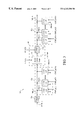
- FIG. 3 shows a 32-bit row 30 in accordance with one embodiment of CAM architecture 20 .
- Row 30 includes two row segments 32 a and 32 b .
- Row segment 32 a includes sixteen CAM cells 10 a ( 1 )- 10 a ( 16 ) each coupled to associated first match line segment ML_a and each receiving one bit of comparand data CMP_a( 1 )-CMP_a( 16 ), respectively.
- Second row segment 32 b includes sixteen CAM cells 10 b ( 1 )- 10 b ( 16 ) each coupled to associated second match line segment ML_b and each receiving one bit of comparand data CMP_b( 1 )-CMP_b( 16 ), respectively.
- Word line(s) and bit line(s) have been omitted from FIG.
- a first charge circuit 34 a pre-charges first match line segment ML_a in response to the logic state of pre-charge signal PCH( 1 ).
- the logic state of first match line segment ML_a which indicates the match condition of first row segment 32 a , is monitored by match detect logic 36 .
- Match detect logic 36 outputs charge signal CH_ 34 b in response to the logic state of first match line segment ML_a and control signal LCT( 1 ).
- Match detect logic 36 outputs CH_ 34 b to a second charge circuit 34 b .
- Charge circuit 34 b pre-charges second match line segment ML_b in response to PCH( 2 ) if CH_ 34 b indicates a match condition for first row segment 32 a .
- match detect logic 36 and charge circuit 34 b form a match line control circuit 40 that selectively pre-charges second match line segment ML_b in response to match conditions in first row segment 32 a.
- match detect logic 36 includes AND logic that drives CH_ 34 b to logic high in response to ML_a being logic high and LCT( 1 ) being logic high. Charge circuit 34 b then pre-charges ML_b when CH_ 34 b is logic high and PCH( 2 ) is asserted.
- Match detect logic 36 may include one or more other logic gates.
- match detect logic 36 includes a well-known latch, and LCT( 1 ) latches the logic state of first match line segment ML_a to generate CH_ 34 b .
- match detect logic 36 may be a voltage level shifter (e.g., a logic gate) that adjusts the voltage level on ML_a to appropriate logic levels for charge circuit 34 b .
- match detect logic 36 may be omitted and ML_a provided to charge circuit 34 b as CH_ 34 b.
- logic similar to match detect logic 36 is provided between PCH( 1 ) and first charge circuit 34 a , and may also receive an enable signal from instruction decoder 22 .
- first match line segment ML_a is pre-charged in response to this enable signal and PCH( 1 ).
- signal CH_ 34 b may also be provided by instruction decoder 22 to pre-charge all row segments during compare operations, thereby allowing match conditions within all row segments to be evaluated simultaneously.
- FIG. 4 shows one example of a timing diagram illustrating a compare operation between a 32-bit comparand word and a 32-bit CAM word stored in row 30 .
- the pre-charge signals PCH( 1 ) and PCH( 2 ) are pulse signals.
- a compare instruction is provided to and subsequently decoded by instruction decoder 22 .
- instruction decoder 22 asserts EN at time t 2 , and causes pre-charge control circuit 25 to assert PCH( 1 ) at time t 3 .
- PCH( 1 ) causes charge circuit 34 a to charge first match line segment ML_a high toward VDD to enable detection of match conditions in first row segment 32 a .
- comparand bits CMP_a( 1 )-CMP_a( 16 ) are then compared with data stored in CAM cells 10 a ( 1 )- 10 a ( 16 ) within first row segment 32 a .
- CMP_a( 1 )-CMP_a( 16 ) may be provided at time t 4 .
- first match line segment ML_a remains pre-charged to a high logic state. If there is a mismatch, then the CAM cell(s) storing the mismatching data pulls ML_a toward a low logic state.
- LCT( 1 ) is asserted to latch or determine the logic state of CH_ 34 b .
- PCH( 2 ) is asserted by pre-charge control circuit 25 .
- second charge circuit 34 b pre-charges second match line segment ML_b toward VDD in response to PCH( 2 ) at time t 7 .
- CMP_b( 1 )-CMP_b( 16 ) are provided to second row segment 32 b at time t 8 .
- CMP_b( 1 )-CMP_b( 16 ) may be provided to the CAM row together with CMP_a( 1 )-CMP_a( 16 ) at time t 4 . If all bit comparisons between CMP_b( 1 )-CMP_b( 16 ) and CAM cells 10 b ( 1 )- 10 b ( 16 ) within second row segment 32 b match, second match line segment ML_b remains in a logic high state to indicate a match condition for second row segment 32 b . Here, there is a match condition for the row.
- first row segment 32 a if any of the bit comparisons in first row segment 32 a mismatch, corresponding CAM cell(s) within first row segment 32 a pull first match line segment ML_a low toward ground potential to indicate a mismatch condition.
- match detect logic 36 maintains signal CH_ 34 b in a logic low state, as indicated by the dashed line in FIG. 4 .
- second charge circuit 34 b does not pre-charge second match line segment ML_b toward V DD .
- Charge circuit 34 b may maintain ML_b in a discharged state.
- mismatch conditions in preceding row segment 32 a force a mismatch condition for subsequent row segment 32 b without pre-charging the subsequent match line segment ML_b.
- power consumption associated with pre-charging the second match line segment is saved.
- present embodiments may reduce power consumption during compare operations.
- Power savings realized by present embodiments are proportional to the number of row segments in the CAM array, as well as to the percentage of mismatch conditions in the first row segments. For instance, where each CAM row is partitioned into two segments having equal numbers of CAM cells as shown in FIG. 3, power consumption resulting from the pre-charging of match lines during compare operations may be reduced, for example, by approximately 50%. When employed in applications where compare operations typically result in mismatch conditions, and in particular where the second and all subsequent match line segments are not usually pre-charged, present embodiments may achieve significant power savings.
- FIG. 5 shows another example of a timing diagram illustrating a compare operation for row 30 .
- pre-charge signals PCH( 1 )-PCH(n) are periodic or clock signals, and the comparand data is provided to row 30 throughout performance of the compare operation.
- This embodiment may alternately have comparand data CMP_a( 1 )-CMP_a( 16 ) provided at a different time from CMP_b( 1 )-CMP_b( 16 ) in FIG. 4 .
- the compare operation of FIG. 5 operates in the same fashion as that of FIG. 4, except that PCH( 1 ) and PCH( 2 ) are clock signals.
- PCH( 1 ) is asserted at time t 2 , and oscillates at approximately the same frequency as CLK.
- PCH( 2 ) is subsequently asserted at time t 3 , and is thereafter approximately 180° out of phase with PCH( 1 ) for the duration of the instruction. If a third row segment is included in row 30 , then it would receive PCH( 3 ) which would be asserted at time t 4 and thereafter be approximately 180° out of phase with respect to PCH( 2 ).
- the periodic pre-charge signals can alternately have any phase relationship with each other so long as each signal is not initially asserted until the preceding row segment has resolved the state of its corresponding match line segment.
- FIG. 6 shows a row 50 in accordance with another embodiment of CAM architecture 20 .
- Row 50 includes two composite row segments 52 a and 52 b each including two (or more) of the 16-bit row segments 32 of FIG. 3 .
- First composite row segment 52 a includes 16-bit row segments 32 a ( 1 ) and 32 a ( 2 )
- second composite row segment 52 b includes 16-bit row segments 32 b ( 1 ) and 32 b ( 2 ).
- Row segments 32 a ( 1 ), 32 a ( 2 ), 32 b ( 1 ), and 32 b ( 2 ) are coupled to associated match line segments ML_a( 1 ), ML_a( 2 ), ML_b( 1 ), and ML_b( 2 ), respectively.
- Charge circuits 34 a ( 1 ) and 34 a ( 2 ) charge match line segments ML_a( 1 ) and ML_a( 2 ) of first and second row segments 32 a ( 1 ) and 32 a ( 2 ), respectively, high toward V DD in response to PCH( 1 ) to enable detection of match conditions within first composite row segment 52 a .
- Match conditions within row segments 32 a ( 1 ) and 32 a ( 2 ) of first composite row segment 52 a are provided to match detect logic 36 a via match line segments ML_a( 1 ) and ML_a( 2 ), respectively.
- Match detect logic 36 a logically combines the logic states of match line segments ML_a( 1 ) and ML_a( 2 ) to generate CH_ 34 b for charge circuits 34 b ( 1 ) and 34 b ( 2 ).
- match detect logic 36 a is an AND or NAND gate.
- Logic 36 a may also include a latch that latches the logical combination of the match line segments ML_a( 1 ) and ML_a( 2 ) in response to LCT( 1 ).
- match detect logic 36 a asserts CH_ 34 b such that charge circuits 34 b ( 1 ) and 34 b ( 2 ) pre-charge match line segments ML_b( 1 ) and ML_b( 2 ), respectively, when PCH( 2 ) is asserted.
- Match conditions within row segments 32 b ( 1 ) and 32 b ( 2 ) of second composite row segment 52 b are then provided to match detect logic 36 b via match line segments ML_b( 1 ) and ML_b( 2 ), respectively.
- match detect logic 36 b logically combines the logic states of the match line segments ML_b( 1 ) and ML_b( 2 ) to provide a match signal for row 50 on match line ML.
- match detect logic 36 b drives the match line ML high to indicate a match condition for row 50 .
- match detect logic 36 b forces match line ML low to indicate a mismatch condition for the row. For example, if first composite row segment 52 a has a mismatch, CH_ 34 b is not asserted and charge circuits 34 b ( 1 ) and 34 b ( 2 ) discharge match line segments ML_b( 1 ) and ML_b( 2 ), respectively. Also, if a mismatch condition is detected in second composite row segment 52 b , one or both of match line segments ML_b( 1 ) and/or ML_b( 2 ) is discharged. When either ML_b( 1 ) or ML_b( 2 ) is discharged, match detect logic 36 b does not assert ML.
- any number of composite row segments may be used, with each having a corresponding match control circuit 40 . If at any point in the sequential evaluation of match conditions in successive row segments there is a mismatch condition, the corresponding match line segment is discharged toward ground potential and, in response thereto, all subsequent match line segments remain uncharged (e.g., are discharged toward ground potential). In this manner, the mismatch condition propagates through subsequent row segments without enabling subsequent match line segments. Thus, if a mismatch condition is detected in the first of the four row segments, only one of the four corresponding match line segments for each row is pre-charged toward V DD , Since the next match line segments are not charged, power consumption associated with charging those match line segments is saved.
- power consumption associated with match line pre-charging during a compare operation may be reduced by approximately 75% when a mismatch condition is detected in the first composite row segment of a row having 4 total composite row segments.
- the reduction in power consumption during the compare operation may be approximately 50%.
- the reduction in power consumption during the compare operation may be approximately 25%.
- Present embodiments may also be effective in applications where the external data bus width is narrower than the CAM array and its internal comparand bus CBUS.
- multiple load operations are required to load a comparand word into a CAM array for compare operations.
- an external 32-bit bus is used to provide 128-bit comparand words to a 128-bit wide CAM array
- four 32-bit load operations are required to load the 128-bit comparand word into the CAM array.
- present embodiments may improve performance by overlapping load and compare operations.
- compare operations may begin on the first 32-bit segment while a second 32-bit segment is loaded. Match conditions within the second 32-bit segment of row 60 may then be evaluated while the third 32-bit segment of the comparand word is loaded, and so on. Accordingly, by executing load and compare operations for such applications in a pipelined fashion, present embodiments may not only reduce power consumption but also achieve performance advantages over prior art structures.
- FIG. 7 shows a row 70 in accordance with still another embodiment of the present invention which provides sequential, asynchronous compare operations.
- pre-charge signals PCH( 1 )-PCH(n) are omitted to provide an asynchronous CAM structure.
- Enable signal EN which as mentioned above may be provided by instruction decoder 22 , is provided directly to charge circuit 34 a to pre-charge match line segment ML_a of first row segment 32 a .
- Match line segment ML_a is connected to second charge circuit 34 b .
- second match line segment ML_b is pre-charged to enable detection of match conditions within second row segment 32 b only in response to the logic state of first match line match segment ML_a.
- FIG. 8 shows a charge circuit 80 that is one embodiment of the charge circuit 34 b of FIG. 3 .
- Charge circuit 80 includes an AC pre-charge circuit 81 , a DC pre-charge circuit 83 , and a discharge transistor 85 .
- DC pre-charge circuit 83 is a weak pre-charge circuit that maintains the pre-charge logic state on ML_b when the relatively strong AC pre-charge circuit 81 has completed its pre-charge operation (i.e., when PCH( 2 ) is de-asserted).
- DC pre-charge circuit 83 includes transistors 82 and 87 coupled in series between V DD and ML_b.
- Transistors 82 and 87 pre-charge ML_b so long as a compare instruction is being performed (i.e., EN logic high), and match detect logic 36 indicates that there is a match condition for a previous row segment (i.e., by asserting CH_ 34 b logic high).
- Weak PMOS transistor 87 has its gate coupled to ⁇ overscore (EN) ⁇ , and weak NMOS transistor 82 has its gate coupled to CH_ 34 b .
- DC pre-charge 83 may be omitted.
- AC pre-charge circuit 81 includes transistors 84 , 86 , and 88 , and pre-charges ML_b when the pre-charge signal PCH( 2 ) is asserted.
- PMOS transistor 84 and NMOS transistor 86 serve as strong pull-up transistors and are connected in series between match line segment ML_b and V DD .
- PMOS transistor 84 has its gate coupled to ⁇ overscore (PCH( 2 )) ⁇ .
- NMOS pass transistor 88 has its gate tied to V DD , and passes CH_ 34 b to the gate of NMOS transistor 86 .
- NMOS transistor 88 is optional, and buffers signal CH_ 34 b from the gate of transistor 86 .
- Discharge transistor 85 is included to discharge ML_b when the preceding row segment indicates a mismatch condition or has not yet resolved its match condition.
- Discharge transistor 85 is an NMOS transistor that has its drain coupled to ML_b, its gate coupled to ⁇ overscore (CH_ 34 b +L ) ⁇ , and its source coupled to ground. Other discharge circuits can be used.
- the gate of transistor 82 may receive EN, and the gate of discharge transistor 85 may have its gate coupled to ⁇ overscore (EN) ⁇ .
- FIG. 9 shows a CAM row 90 that is one embodiment of CAM 20 of FIG. 2 configured to implement a class searching function.
- Row 90 includes a first row segment 92 having a first number of CAM cells designated as class cells, and a second row segment 94 having a second number of CAM cells designated as data cells.
- the class and data cells of FIG. 9 are of the type shown in FIG. 1, although in other embodiments other suitable CAM cells may be used, including ternary CAM cells.
- Data cells in data segment 94 store data such as Internet addresses, while class cells in class segment 92 store class information which indicates to which class corresponding data belongs.
- Match line segments (not shown for simplicity) in class segment 92 are pre-charged toward V DD by charge circuit 34 in response to pre-charge signal PCH( 1 ) in the manner described above with respect to FIGS. 3 and 4.
- match line segments in corresponding data segment 94 are pre-charged toward V DD to enable detection of match conditions in data segment 94 . If, on the other hand, there is a mismatch condition in class segment 92 , match lines within corresponding data segment 94 are not pre-charged to force a mismatch condition for the row. In this manner, data stored in data cells of data segment 94 may be initially be searched according to class and, if there is a match, then searched according to data. Accordingly, the selective pre-charging of match line segments in data segment 94 not only reduces power consumption during compare operations, but also allows for sequential searching based upon a plurality of pre-defined classes. In this manner, present embodiments may implement a dynamic masking function based upon class matches, e.g., match conditions in preceding row segments.
- data segment 94 may store a 32-bit or 128-bit Internet Protocol (IP) address, while class segment 92 indicates to which of 16 classes the corresponding IP address belongs.
- IP Internet Protocol
- the classes may indicate suitable information about the corresponding address such as, for instance, a virtual private network (VPN) identifier or an identifier for protocol-based applications.
- VPN virtual private network
- embodiments of FIG. 9 allow for address entries stored within data segment 94 to be first searched for a class match, and then subsequently searched for an address match. Comparison may be performed in a single clock cycle or in multiple clock cycles.
- match line segments corresponding to only 4 of the CAM cells in row are initially pre-charged for compare operations, and thus the match line segment(s) corresponding to the remaining 32 or 128 CAM cells in row 90 are not pre-charged, power consumption associated with match line pre-charging may be significantly reduced over prior art structures.
- CAMs in accordance with present embodiments may include any suitable number of row segments each of having any suitable number of cells.
Abstract
Description
Claims (40)
Priority Applications (2)
| Application Number | Priority Date | Filing Date | Title |
|---|---|---|---|
| US09/391,989 US6243280B1 (en) | 1999-09-09 | 1999-09-09 | Selective match line pre-charging in a partitioned content addressable memory array |
| US09/813,900 US6430074B1 (en) | 1999-09-09 | 2001-03-20 | Selective look-ahead match line pre-charging in a partitioned content addressable memory array |
Applications Claiming Priority (1)
| Application Number | Priority Date | Filing Date | Title |
|---|---|---|---|
| US09/391,989 US6243280B1 (en) | 1999-09-09 | 1999-09-09 | Selective match line pre-charging in a partitioned content addressable memory array |
Related Child Applications (1)
| Application Number | Title | Priority Date | Filing Date |
|---|---|---|---|
| US09/813,900 Continuation-In-Part US6430074B1 (en) | 1999-09-09 | 2001-03-20 | Selective look-ahead match line pre-charging in a partitioned content addressable memory array |
Publications (1)
| Publication Number | Publication Date |
|---|---|
| US6243280B1 true US6243280B1 (en) | 2001-06-05 |
Family
ID=23548811
Family Applications (1)
| Application Number | Title | Priority Date | Filing Date |
|---|---|---|---|
| US09/391,989 Expired - Lifetime US6243280B1 (en) | 1999-09-09 | 1999-09-09 | Selective match line pre-charging in a partitioned content addressable memory array |
Country Status (1)
| Country | Link |
|---|---|
| US (1) | US6243280B1 (en) |
Cited By (66)
| Publication number | Priority date | Publication date | Assignee | Title |
|---|---|---|---|---|
| US6349049B1 (en) * | 2001-03-22 | 2002-02-19 | Sun Microsystems, Inc. | High speed low power content addressable memory |
| US20020161969A1 (en) * | 1999-09-23 | 2002-10-31 | Nataraj Bindiganavale S. | Content addressable memory with programmable word width and programmable priority |
| US6496398B2 (en) * | 2000-12-15 | 2002-12-17 | International Business Machines Corporation | Content addressable memory |
| US20030093616A1 (en) * | 2001-11-01 | 2003-05-15 | Slavin Keith R. | Low power, hash-content addressable memory architecture |
| WO2003050819A1 (en) * | 2001-12-11 | 2003-06-19 | Memcall L.L.C. | Power saving cam |
| US6584003B1 (en) | 2001-12-28 | 2003-06-24 | Mosaid Technologies Incorporated | Low power content addressable memory architecture |
| US20030123269A1 (en) * | 2001-12-31 | 2003-07-03 | Peter Gillingham | Circuit and method for reducing power usage in a content addressable memory |
| WO2003056564A1 (en) * | 2001-12-28 | 2003-07-10 | Mosaid Technologies Incorporated | Low power content addressable memory architecture |
| US6615210B1 (en) * | 2000-02-04 | 2003-09-02 | Broad Web Corporation | Bit stream ternary match scheme |
| US20040008533A1 (en) * | 2001-01-10 | 2004-01-15 | Fujitsu Limited | Associative memory |
| US6760242B1 (en) | 2002-04-10 | 2004-07-06 | Integrated Device Technology, Inc. | Content addressable memory (CAM) devices having speed adjustable match line signal repeaters therein |
| US6801981B1 (en) | 2000-06-14 | 2004-10-05 | Netlogic Microsystems, Inc. | Intra-row configurability of content addressable memory |
| US6804133B1 (en) | 2002-08-30 | 2004-10-12 | Netlogic Microsystems, Inc. | Selective match line control circuit for content addressable memory array |
| US6813680B1 (en) | 2000-06-14 | 2004-11-02 | Netlogic Microsystems, Inc. | Method and apparatus for loading comparand data into a content addressable memory system |
| US6839256B1 (en) | 2002-03-15 | 2005-01-04 | Integrated Device Technology, Inc. | Content addressable memory (CAM) devices having dedicated mask cell sub-arrays therein and methods of operating same |
| US6867991B1 (en) | 2003-07-03 | 2005-03-15 | Integrated Device Technology, Inc. | Content addressable memory devices with virtual partitioning and methods of operating the same |
| US6879532B1 (en) | 2002-04-10 | 2005-04-12 | Integrated Device Technology, Inc. | Content addressable and random access memory devices having high-speed sense amplifiers therein with low power consumption requirements |
| US6903953B2 (en) | 2002-08-01 | 2005-06-07 | Netlogic Microsystems, Inc. | Content addressable memory with cascaded array |
| US20050213359A1 (en) * | 2004-03-26 | 2005-09-29 | Kim Jin K | Hybrid content addressable memory |
| US6965519B1 (en) | 2003-06-18 | 2005-11-15 | Integrated Device Technology, Inc. | Content addressable memory (CAM) devices that utilize dual-capture match line signal repeaters to achieve desired speed/power tradeoff and methods of operating same |
| US6967856B1 (en) | 2002-04-10 | 2005-11-22 | Integrated Device Technology, Inc. | Content addressable memory (CAM) devices that utilize segmented match lines and word lines to support pipelined search and write operations and methods of operating same |
| US6972978B1 (en) | 2002-03-15 | 2005-12-06 | Integrated Device Technology, Inc. | Content addressable memory (CAM) devices with block select and pipelined virtual sector look-up control and methods of operating same |
| US20060018141A1 (en) * | 2004-07-26 | 2006-01-26 | International Business Machines Corporation | Apparatus and method for power savings in high-performance CAM structures |
| US7050317B1 (en) | 2002-03-15 | 2006-05-23 | Integrated Device Technology, Inc. | Content addressable memory (CAM) devices that support power saving longest prefix match operations and methods of operating same |
| US20060143374A1 (en) * | 2004-12-29 | 2006-06-29 | Sailesh Kottapalli | Pipelined look-up in a content addressable memory |
| US7084672B1 (en) * | 2003-06-27 | 2006-08-01 | Meng Anita X | Sense amplifier circuit for content addressable memory device |
| US20060176722A1 (en) * | 2004-10-12 | 2006-08-10 | Ripy Paul B | Method of operating a content addressable memory with reduced instantaneous current and power consumption during a search |
| US7113415B1 (en) * | 2004-06-01 | 2006-09-26 | Netlogic Microsystems, Inc. | Match line pre-charging in a content addressable memory having configurable rows |
| US7126834B1 (en) | 2003-09-12 | 2006-10-24 | Netlogic Microsystems, Inc. | Sense amplifier architecture for content addressable memory device |
| US7185141B1 (en) | 2001-12-27 | 2007-02-27 | Netlogic Microsystems, Inc. | Apparatus and method for associating information values with portions of a content addressable memory (CAM) device |
| US20070066651A1 (en) * | 2004-02-16 | 2007-03-22 | Laboratorios Del Dr. Esteve S.A. | Pyrazoline derivatives useful for the treatment of cancer |
| US20070165435A1 (en) * | 2006-01-19 | 2007-07-19 | Winograd Gil I | Low-power CAM |
| US20080031033A1 (en) * | 2006-08-04 | 2008-02-07 | Chiaming Chai | Method and Apparatus for Reducing Power Consumption in a Content Addressable Memory |
| US20080031040A1 (en) * | 2006-08-04 | 2008-02-07 | Chiaming Chai | Method and Apparatus for Aborting Content Addressable Memory Search Operations |
| US7362602B1 (en) | 2005-08-08 | 2008-04-22 | Netlogic Microsystems, Inc. | Sense amplifier circuit and method |
| US7401180B1 (en) | 2001-12-27 | 2008-07-15 | Netlogic Microsystems, Inc. | Content addressable memory (CAM) device having selectable access and method therefor |
| US20090083499A1 (en) * | 2007-09-24 | 2009-03-26 | Nvidia Corporation | Ordered Storage Structure Providing Enhanced Access to Stored Items |
| US20090153108A1 (en) * | 2007-12-17 | 2009-06-18 | Neil Hendin | Power management efficiency using DC-DC and linear regulators in conjunction |
| US20090153211A1 (en) * | 2007-12-17 | 2009-06-18 | Neil Hendin | Integrated circuit device core power down independent of peripheral device operation |
| US7590815B1 (en) | 2002-08-30 | 2009-09-15 | Nvidia Corporation | Method and apparatus for partial memory power shutoff |
| USRE40932E1 (en) | 1999-07-27 | 2009-10-06 | Netlogic Microsystems, Inc. | Content addressable memory (CAM) devices that perform pipelined multi-cycle look-up operations using cam sub-arrays and longest match detection |
| US20090259863A1 (en) * | 2008-04-10 | 2009-10-15 | Nvidia Corporation | Responding to interrupts while in a reduced power state |
| USRE41351E1 (en) | 2000-05-18 | 2010-05-25 | Netlogic Microsystems, Inc. | CAM arrays having CAM cells therein with match line and low match line connections and methods of operating same |
| US7800930B1 (en) | 2008-02-06 | 2010-09-21 | Netlogic Microsystems, Inc. | Precharge circuits and methods for content addressable memory (CAM) and related devices |
| US7920397B1 (en) | 2010-04-30 | 2011-04-05 | Netlogic Microsystems, Inc. | Memory device having bit line leakage compensation |
| US7920399B1 (en) | 2010-10-21 | 2011-04-05 | Netlogic Microsystems, Inc. | Low power content addressable memory device having selectable cascaded array segments |
| US7920398B1 (en) | 2010-09-21 | 2011-04-05 | Netlogic Microsystems, Inc. | Adaptive match line charging |
| US7944724B2 (en) | 2009-04-28 | 2011-05-17 | Netlogic Microsystems, Inc. | Ternary content addressable memory having reduced leakage effects |
| US8031501B1 (en) | 2010-10-21 | 2011-10-04 | Netlogic Microsystems, Inc. | Segmented content addressable memory device having pipelined compare operations |
| US8073005B1 (en) | 2001-12-27 | 2011-12-06 | Cypress Semiconductor Corporation | Method and apparatus for configuring signal lines according to idle codes |
| US20120233415A1 (en) * | 2011-02-23 | 2012-09-13 | Huawei Technologies Co., Ltd. | Method and apparatus for searching for data in memory, and memory |
| US8467213B1 (en) | 2011-03-22 | 2013-06-18 | Netlogic Microsystems, Inc. | Power limiting in a content search system |
| US8493763B1 (en) | 2011-10-27 | 2013-07-23 | Netlogic Microsystems, Inc. | Self-timed match line cascading in a partitioned content addressable memory array |
| US8619451B1 (en) | 2012-01-06 | 2013-12-31 | Netlogic Microsystems, Inc. | Power savings in a content addressable memory device using masked pre-compare operations |
| US8773880B2 (en) | 2011-06-23 | 2014-07-08 | Netlogic Microsystems, Inc. | Content addressable memory array having virtual ground nodes |
| US8787059B1 (en) | 2011-12-05 | 2014-07-22 | Netlogic Microsystems, Inc. | Cascaded content addressable memory array having multiple row segment activation |
| US8837188B1 (en) | 2011-06-23 | 2014-09-16 | Netlogic Microsystems, Inc. | Content addressable memory row having virtual ground and charge sharing |
| US8913412B1 (en) | 2011-11-29 | 2014-12-16 | Netlogic Microsystems, Inc. | Incremental adaptive match line charging with calibration |
| JP2015523670A (en) * | 2012-05-29 | 2015-08-13 | インターナショナル・ビジネス・マシーンズ・コーポレーションInternational Business Machines Corporation | System and method for retrieving content addressable memory (CAM) |
| US9411390B2 (en) | 2008-02-11 | 2016-08-09 | Nvidia Corporation | Integrated circuit device having power domains and partitions based on use case power optimization |
| US9423846B2 (en) | 2008-04-10 | 2016-08-23 | Nvidia Corporation | Powered ring to maintain IO state independent of the core of an integrated circuit device |
| US9471395B2 (en) | 2012-08-23 | 2016-10-18 | Nvidia Corporation | Processor cluster migration techniques |
| US9742396B2 (en) | 2012-09-05 | 2017-08-22 | Nvidia Corporation | Core voltage reset systems and methods with wide noise margin |
| CN110729013A (en) * | 2018-07-16 | 2020-01-24 | 联华电子股份有限公司 | Control circuit for tri-state content addressable memory |
| EP3832654A1 (en) * | 2019-12-03 | 2021-06-09 | MediaTek Singapore Pte Ltd | Low-power multi-stage/multi-segment content addressable memory device |
| US11342022B2 (en) | 2019-12-03 | 2022-05-24 | Mediatek Singapore Pte. Ltd. | Low-power multi-stage/multi-segment content addressable memory device |
Citations (4)
| Publication number | Priority date | Publication date | Assignee | Title |
|---|---|---|---|---|
| US5483480A (en) | 1993-07-22 | 1996-01-09 | Kawasaki Steel Corporation | Method of using associative memories and an associative memory |
| US5517441A (en) | 1994-12-14 | 1996-05-14 | International Business Machines Corporation | Content addressable memory circuitry and method of operation |
| US5659697A (en) * | 1994-12-14 | 1997-08-19 | International Business Machines Corporation | Translation lookaside buffer for faster processing in response to availability of a first virtual address portion before a second virtual address portion |
| US5978246A (en) | 1997-09-08 | 1999-11-02 | Nec Corporation | Content addressable memory device |
-
1999
- 1999-09-09 US US09/391,989 patent/US6243280B1/en not_active Expired - Lifetime
Patent Citations (4)
| Publication number | Priority date | Publication date | Assignee | Title |
|---|---|---|---|---|
| US5483480A (en) | 1993-07-22 | 1996-01-09 | Kawasaki Steel Corporation | Method of using associative memories and an associative memory |
| US5517441A (en) | 1994-12-14 | 1996-05-14 | International Business Machines Corporation | Content addressable memory circuitry and method of operation |
| US5659697A (en) * | 1994-12-14 | 1997-08-19 | International Business Machines Corporation | Translation lookaside buffer for faster processing in response to availability of a first virtual address portion before a second virtual address portion |
| US5978246A (en) | 1997-09-08 | 1999-11-02 | Nec Corporation | Content addressable memory device |
Cited By (97)
| Publication number | Priority date | Publication date | Assignee | Title |
|---|---|---|---|---|
| USRE40932E1 (en) | 1999-07-27 | 2009-10-06 | Netlogic Microsystems, Inc. | Content addressable memory (CAM) devices that perform pipelined multi-cycle look-up operations using cam sub-arrays and longest match detection |
| US20020161969A1 (en) * | 1999-09-23 | 2002-10-31 | Nataraj Bindiganavale S. | Content addressable memory with programmable word width and programmable priority |
| US6615210B1 (en) * | 2000-02-04 | 2003-09-02 | Broad Web Corporation | Bit stream ternary match scheme |
| USRE41351E1 (en) | 2000-05-18 | 2010-05-25 | Netlogic Microsystems, Inc. | CAM arrays having CAM cells therein with match line and low match line connections and methods of operating same |
| US6813680B1 (en) | 2000-06-14 | 2004-11-02 | Netlogic Microsystems, Inc. | Method and apparatus for loading comparand data into a content addressable memory system |
| US6801981B1 (en) | 2000-06-14 | 2004-10-05 | Netlogic Microsystems, Inc. | Intra-row configurability of content addressable memory |
| US6496398B2 (en) * | 2000-12-15 | 2002-12-17 | International Business Machines Corporation | Content addressable memory |
| US6885571B2 (en) * | 2001-01-10 | 2005-04-26 | Fujitsu Limited | Associative memory having a search bus driving circuit for supplying search data to associative memory cells |
| JP4511790B2 (en) * | 2001-01-10 | 2010-07-28 | 富士通セミコンダクター株式会社 | Associative memory |
| US20040008533A1 (en) * | 2001-01-10 | 2004-01-15 | Fujitsu Limited | Associative memory |
| JPWO2002056315A1 (en) * | 2001-01-10 | 2004-05-20 | 富士通株式会社 | Associative memory |
| US6349049B1 (en) * | 2001-03-22 | 2002-02-19 | Sun Microsystems, Inc. | High speed low power content addressable memory |
| US8112578B2 (en) | 2001-11-01 | 2012-02-07 | Micron Technology, Inc. | Low power, hash-content addressable memory architecture |
| US8788791B2 (en) | 2001-11-01 | 2014-07-22 | Micron Technology, Inc. | Low power, hash-content addressable memory architecture |
| US8949574B2 (en) | 2001-11-01 | 2015-02-03 | Micron Technology, Inc. | Low power, hash-content addressable memory architecture |
| US20030093616A1 (en) * | 2001-11-01 | 2003-05-15 | Slavin Keith R. | Low power, hash-content addressable memory architecture |
| WO2003050819A1 (en) * | 2001-12-11 | 2003-06-19 | Memcall L.L.C. | Power saving cam |
| US7185141B1 (en) | 2001-12-27 | 2007-02-27 | Netlogic Microsystems, Inc. | Apparatus and method for associating information values with portions of a content addressable memory (CAM) device |
| US7401180B1 (en) | 2001-12-27 | 2008-07-15 | Netlogic Microsystems, Inc. | Content addressable memory (CAM) device having selectable access and method therefor |
| US8073005B1 (en) | 2001-12-27 | 2011-12-06 | Cypress Semiconductor Corporation | Method and apparatus for configuring signal lines according to idle codes |
| WO2003056564A1 (en) * | 2001-12-28 | 2003-07-10 | Mosaid Technologies Incorporated | Low power content addressable memory architecture |
| CN100414646C (en) * | 2001-12-28 | 2008-08-27 | 莫塞德技术公司 | Low power content addressable memory architecture |
| US6584003B1 (en) | 2001-12-28 | 2003-06-24 | Mosaid Technologies Incorporated | Low power content addressable memory architecture |
| US6768659B2 (en) | 2001-12-31 | 2004-07-27 | Mosaid Technologies Incorporated | Circuit and method for reducing power usage in a content addressable memory |
| US20030123269A1 (en) * | 2001-12-31 | 2003-07-03 | Peter Gillingham | Circuit and method for reducing power usage in a content addressable memory |
| US6972978B1 (en) | 2002-03-15 | 2005-12-06 | Integrated Device Technology, Inc. | Content addressable memory (CAM) devices with block select and pipelined virtual sector look-up control and methods of operating same |
| US7050317B1 (en) | 2002-03-15 | 2006-05-23 | Integrated Device Technology, Inc. | Content addressable memory (CAM) devices that support power saving longest prefix match operations and methods of operating same |
| US6839256B1 (en) | 2002-03-15 | 2005-01-04 | Integrated Device Technology, Inc. | Content addressable memory (CAM) devices having dedicated mask cell sub-arrays therein and methods of operating same |
| US6879532B1 (en) | 2002-04-10 | 2005-04-12 | Integrated Device Technology, Inc. | Content addressable and random access memory devices having high-speed sense amplifiers therein with low power consumption requirements |
| US6760242B1 (en) | 2002-04-10 | 2004-07-06 | Integrated Device Technology, Inc. | Content addressable memory (CAM) devices having speed adjustable match line signal repeaters therein |
| US6967856B1 (en) | 2002-04-10 | 2005-11-22 | Integrated Device Technology, Inc. | Content addressable memory (CAM) devices that utilize segmented match lines and word lines to support pipelined search and write operations and methods of operating same |
| US6775168B1 (en) | 2002-04-10 | 2004-08-10 | Integrated Device Technology, Inc. | Content addressable memory (CAM) devices having adjustable match line precharge circuits therein |
| US6804134B1 (en) | 2002-04-10 | 2004-10-12 | Integrated Device Technology, Inc. | Content addressable memory (CAM) devices having CAM array blocks therein that conserve bit line power during staged compare operations |
| US6829153B1 (en) | 2002-04-10 | 2004-12-07 | Integrated Device Technology, Inc. | Content addressable memory (CAM) devices having CAM array blocks therein that perform pipelined and interleaved search, write and read operations and methods of operating same |
| US6903953B2 (en) | 2002-08-01 | 2005-06-07 | Netlogic Microsystems, Inc. | Content addressable memory with cascaded array |
| US7042748B2 (en) | 2002-08-01 | 2006-05-09 | Netlogic Microsystems, Inc. | Content addressable memory with cascaded array |
| US20050169031A1 (en) * | 2002-08-01 | 2005-08-04 | Sandeep Khanna | Content addressable memory with cascaded array |
| US7590815B1 (en) | 2002-08-30 | 2009-09-15 | Nvidia Corporation | Method and apparatus for partial memory power shutoff |
| US6804133B1 (en) | 2002-08-30 | 2004-10-12 | Netlogic Microsystems, Inc. | Selective match line control circuit for content addressable memory array |
| US6965519B1 (en) | 2003-06-18 | 2005-11-15 | Integrated Device Technology, Inc. | Content addressable memory (CAM) devices that utilize dual-capture match line signal repeaters to achieve desired speed/power tradeoff and methods of operating same |
| US7084672B1 (en) * | 2003-06-27 | 2006-08-01 | Meng Anita X | Sense amplifier circuit for content addressable memory device |
| US6867991B1 (en) | 2003-07-03 | 2005-03-15 | Integrated Device Technology, Inc. | Content addressable memory devices with virtual partitioning and methods of operating the same |
| US7126834B1 (en) | 2003-09-12 | 2006-10-24 | Netlogic Microsystems, Inc. | Sense amplifier architecture for content addressable memory device |
| US20070066651A1 (en) * | 2004-02-16 | 2007-03-22 | Laboratorios Del Dr. Esteve S.A. | Pyrazoline derivatives useful for the treatment of cancer |
| US8031502B2 (en) | 2004-03-26 | 2011-10-04 | Mosaid Technologies Incorporated | Hybrid content addressable memory |
| US20050213359A1 (en) * | 2004-03-26 | 2005-09-29 | Kim Jin K | Hybrid content addressable memory |
| US20090190386A1 (en) * | 2004-03-26 | 2009-07-30 | Mosaid Technologies Incorporated | Hybrid content addressable memory |
| US7113415B1 (en) * | 2004-06-01 | 2006-09-26 | Netlogic Microsystems, Inc. | Match line pre-charging in a content addressable memory having configurable rows |
| US7079409B2 (en) | 2004-07-26 | 2006-07-18 | International Business Machines Corporation | Apparatus and method for power savings in high-performance CAM structures |
| US20060018141A1 (en) * | 2004-07-26 | 2006-01-26 | International Business Machines Corporation | Apparatus and method for power savings in high-performance CAM structures |
| US20060176722A1 (en) * | 2004-10-12 | 2006-08-10 | Ripy Paul B | Method of operating a content addressable memory with reduced instantaneous current and power consumption during a search |
| US20060143374A1 (en) * | 2004-12-29 | 2006-06-29 | Sailesh Kottapalli | Pipelined look-up in a content addressable memory |
| US7362602B1 (en) | 2005-08-08 | 2008-04-22 | Netlogic Microsystems, Inc. | Sense amplifier circuit and method |
| US7414873B2 (en) | 2006-01-19 | 2008-08-19 | Novelics, Llc | Low-power CAM cell |
| US7400520B2 (en) * | 2006-01-19 | 2008-07-15 | Norvelics, Llc | Low-power CAM |
| US20070165435A1 (en) * | 2006-01-19 | 2007-07-19 | Winograd Gil I | Low-power CAM |
| US20080137387A1 (en) * | 2006-01-19 | 2008-06-12 | Winograd Gil I | Low-power cam cell |
| US20080031033A1 (en) * | 2006-08-04 | 2008-02-07 | Chiaming Chai | Method and Apparatus for Reducing Power Consumption in a Content Addressable Memory |
| US7616468B2 (en) * | 2006-08-04 | 2009-11-10 | Qualcomm Incorporated | Method and apparatus for reducing power consumption in a content addressable memory |
| US20100023684A1 (en) * | 2006-08-04 | 2010-01-28 | Qualcomm Incorporated | Method and apparatus for reducing power consumption in a content addressable memory |
| US7586772B2 (en) * | 2006-08-04 | 2009-09-08 | Qualcomm Incorporated | Method and apparatus for aborting content addressable memory search operations |
| US8154900B2 (en) * | 2006-08-04 | 2012-04-10 | Qualcomm Incorporated | Method and apparatus for reducing power consumption in a content addressable memory |
| US20080031040A1 (en) * | 2006-08-04 | 2008-02-07 | Chiaming Chai | Method and Apparatus for Aborting Content Addressable Memory Search Operations |
| US20090083499A1 (en) * | 2007-09-24 | 2009-03-26 | Nvidia Corporation | Ordered Storage Structure Providing Enhanced Access to Stored Items |
| US8255623B2 (en) | 2007-09-24 | 2012-08-28 | Nvidia Corporation | Ordered storage structure providing enhanced access to stored items |
| US8327173B2 (en) | 2007-12-17 | 2012-12-04 | Nvidia Corporation | Integrated circuit device core power down independent of peripheral device operation |
| US20090153108A1 (en) * | 2007-12-17 | 2009-06-18 | Neil Hendin | Power management efficiency using DC-DC and linear regulators in conjunction |
| US20090153211A1 (en) * | 2007-12-17 | 2009-06-18 | Neil Hendin | Integrated circuit device core power down independent of peripheral device operation |
| US9088176B2 (en) | 2007-12-17 | 2015-07-21 | Nvidia Corporation | Power management efficiency using DC-DC and linear regulators in conjunction |
| US7800930B1 (en) | 2008-02-06 | 2010-09-21 | Netlogic Microsystems, Inc. | Precharge circuits and methods for content addressable memory (CAM) and related devices |
| US8089794B1 (en) | 2008-02-06 | 2012-01-03 | Netlogic Microsystems, Inc. | Precharge circuits and methods for content addressable memory (CAM) and related devices |
| US9411390B2 (en) | 2008-02-11 | 2016-08-09 | Nvidia Corporation | Integrated circuit device having power domains and partitions based on use case power optimization |
| US20090259863A1 (en) * | 2008-04-10 | 2009-10-15 | Nvidia Corporation | Responding to interrupts while in a reduced power state |
| US9423846B2 (en) | 2008-04-10 | 2016-08-23 | Nvidia Corporation | Powered ring to maintain IO state independent of the core of an integrated circuit device |
| US8762759B2 (en) | 2008-04-10 | 2014-06-24 | Nvidia Corporation | Responding to interrupts while in a reduced power state |
| US7944724B2 (en) | 2009-04-28 | 2011-05-17 | Netlogic Microsystems, Inc. | Ternary content addressable memory having reduced leakage effects |
| US7920397B1 (en) | 2010-04-30 | 2011-04-05 | Netlogic Microsystems, Inc. | Memory device having bit line leakage compensation |
| US7920398B1 (en) | 2010-09-21 | 2011-04-05 | Netlogic Microsystems, Inc. | Adaptive match line charging |
| US7920399B1 (en) | 2010-10-21 | 2011-04-05 | Netlogic Microsystems, Inc. | Low power content addressable memory device having selectable cascaded array segments |
| US8031501B1 (en) | 2010-10-21 | 2011-10-04 | Netlogic Microsystems, Inc. | Segmented content addressable memory device having pipelined compare operations |
| US20120233415A1 (en) * | 2011-02-23 | 2012-09-13 | Huawei Technologies Co., Ltd. | Method and apparatus for searching for data in memory, and memory |
| US9025354B2 (en) | 2011-03-22 | 2015-05-05 | Broadcom Corporation | Power limiting in a content search system |
| US8467213B1 (en) | 2011-03-22 | 2013-06-18 | Netlogic Microsystems, Inc. | Power limiting in a content search system |
| US8837188B1 (en) | 2011-06-23 | 2014-09-16 | Netlogic Microsystems, Inc. | Content addressable memory row having virtual ground and charge sharing |
| US8773880B2 (en) | 2011-06-23 | 2014-07-08 | Netlogic Microsystems, Inc. | Content addressable memory array having virtual ground nodes |
| US8493763B1 (en) | 2011-10-27 | 2013-07-23 | Netlogic Microsystems, Inc. | Self-timed match line cascading in a partitioned content addressable memory array |
| US8913412B1 (en) | 2011-11-29 | 2014-12-16 | Netlogic Microsystems, Inc. | Incremental adaptive match line charging with calibration |
| US8787059B1 (en) | 2011-12-05 | 2014-07-22 | Netlogic Microsystems, Inc. | Cascaded content addressable memory array having multiple row segment activation |
| US9019737B2 (en) | 2012-01-06 | 2015-04-28 | Broadcom Corporation | Power savings in a content addressable memory device using masked pre-compare operations |
| US8619451B1 (en) | 2012-01-06 | 2013-12-31 | Netlogic Microsystems, Inc. | Power savings in a content addressable memory device using masked pre-compare operations |
| JP2015523670A (en) * | 2012-05-29 | 2015-08-13 | インターナショナル・ビジネス・マシーンズ・コーポレーションInternational Business Machines Corporation | System and method for retrieving content addressable memory (CAM) |
| US9471395B2 (en) | 2012-08-23 | 2016-10-18 | Nvidia Corporation | Processor cluster migration techniques |
| US9742396B2 (en) | 2012-09-05 | 2017-08-22 | Nvidia Corporation | Core voltage reset systems and methods with wide noise margin |
| CN110729013A (en) * | 2018-07-16 | 2020-01-24 | 联华电子股份有限公司 | Control circuit for tri-state content addressable memory |
| CN110729013B (en) * | 2018-07-16 | 2021-10-29 | 蓝枪半导体有限责任公司 | Control circuit for tri-state content addressable memory |
| EP3832654A1 (en) * | 2019-12-03 | 2021-06-09 | MediaTek Singapore Pte Ltd | Low-power multi-stage/multi-segment content addressable memory device |
| US11342022B2 (en) | 2019-12-03 | 2022-05-24 | Mediatek Singapore Pte. Ltd. | Low-power multi-stage/multi-segment content addressable memory device |
Similar Documents
| Publication | Publication Date | Title |
|---|---|---|
| US6243280B1 (en) | Selective match line pre-charging in a partitioned content addressable memory array | |
| US6430074B1 (en) | Selective look-ahead match line pre-charging in a partitioned content addressable memory array | |
| US6191970B1 (en) | Selective match line discharging in a partitioned content addressable memory array | |
| US6240485B1 (en) | Method and apparatus for implementing a learn instruction in a depth cascaded content addressable memory system | |
| US6418042B1 (en) | Ternary content addressable memory with compare operand selected according to mask value | |
| US6768659B2 (en) | Circuit and method for reducing power usage in a content addressable memory | |
| US6219748B1 (en) | Method and apparatus for implementing a learn instruction in a content addressable memory device | |
| US6460112B1 (en) | Method and apparatus for determining a longest prefix match in a content addressable memory device | |
| US6147891A (en) | Match line control circuit for content addressable memory | |
| US6148364A (en) | Method and apparatus for cascading content addressable memory devices | |
| US6584003B1 (en) | Low power content addressable memory architecture | |
| US7042748B2 (en) | Content addressable memory with cascaded array | |
| US7751272B2 (en) | Semiconductor device and method for selection and de-selection of memory devices interconnected in series | |
| US6499081B1 (en) | Method and apparatus for determining a longest prefix match in a segmented content addressable memory device | |
| US6597596B2 (en) | Content addressable memory having cascaded sub-entry architecture | |
| USRE43359E1 (en) | System and method for low power searching in content addressable memories using sampling search words to save power in compare lines | |
| US20030028713A1 (en) | Method and apparatus for determining an exact match in a ternary content addressable memory device | |
| WO2021021507A1 (en) | Sram with burst mode address comparator | |
| US6349049B1 (en) | High speed low power content addressable memory | |
| US7113415B1 (en) | Match line pre-charging in a content addressable memory having configurable rows | |
| US7400520B2 (en) | Low-power CAM | |
| US5754463A (en) | Multi-ported content addressable memory with precharge "non match" | |
| WO1999023663A1 (en) | Synchronous content addressable memory with single cycle operation | |
| JPH11512551A (en) | High-speed word line decoder for memory devices | |
| JP2779114B2 (en) | Associative memory |
Legal Events
| Date | Code | Title | Description |
|---|---|---|---|
| AS | Assignment |
Owner name: NETLOGIC MICROSYSTEMS, INC., CALIFORNIA Free format text: ASSIGNMENT OF ASSIGNORS INTEREST;ASSIGNORS:WONG, HOK F.;PEREIRA, JOSE P.;SRINIVASAN, VARADARAJAN;REEL/FRAME:010944/0185 Effective date: 20000615 |
|
| STCF | Information on status: patent grant |
Free format text: PATENTED CASE |
|
| AS | Assignment |
Owner name: SILICON VALLEY BANK, CALIFORNIA Free format text: SECURITY AGREEMENT;ASSIGNOR:NETLOGIC MICROSYSTEMS, INC.;REEL/FRAME:015201/0812 Effective date: 20040330 |
|
| FPAY | Fee payment |
Year of fee payment: 4 |
|
| AS | Assignment |
Owner name: NETLOGIC MICROSYSTEMS, INC., CALIFORNIA Free format text: RELEASE;ASSIGNOR:SILICON VALLEY BANK;REEL/FRAME:018420/0760 Effective date: 20060919 |
|
| FPAY | Fee payment |
Year of fee payment: 8 |
|
| AS | Assignment |
Owner name: SILICON VALLEY BANK, CALIFORNIA Free format text: SECURITY AGREEMENT;ASSIGNORS:NETLOGIC MICROSYSTEMS, INC.;NETLOGIC MICROSYSTEMS INTERNATIONAL LIMITED;NETLOGIC MICROSYSTEMS CAYMANS LIMITED;REEL/FRAME:022973/0710 Effective date: 20090717 Owner name: SILICON VALLEY BANK,CALIFORNIA Free format text: SECURITY AGREEMENT;ASSIGNORS:NETLOGIC MICROSYSTEMS, INC.;NETLOGIC MICROSYSTEMS INTERNATIONAL LIMITED;NETLOGIC MICROSYSTEMS CAYMANS LIMITED;REEL/FRAME:022973/0710 Effective date: 20090717 |
|
| FEPP | Fee payment procedure |
Free format text: PAYER NUMBER DE-ASSIGNED (ORIGINAL EVENT CODE: RMPN); ENTITY STATUS OF PATENT OWNER: LARGE ENTITY Free format text: PAYOR NUMBER ASSIGNED (ORIGINAL EVENT CODE: ASPN); ENTITY STATUS OF PATENT OWNER: LARGE ENTITY |
|
| AS | Assignment |
Owner name: NETLOGIC MICROSYSTEMS, INC., CALIFORNIA Free format text: RELEASE;ASSIGNOR:SILICON VALLEY BANK;REEL/FRAME:025077/0977 Effective date: 20100809 |
|
| AS | Assignment |
Owner name: NETLOGIC MICROSYSTEMS INTERNATIONAL LIMITED, CALIF Free format text: RELEASE;ASSIGNOR:SILICON VALLEY BANK;REEL/FRAME:025051/0248 Effective date: 20100809 Owner name: NETLOGIC MICROSYSTEMS, INC., CALIFORNIA Free format text: RELEASE;ASSIGNOR:SILICON VALLEY BANK;REEL/FRAME:025051/0248 Effective date: 20100809 Owner name: NETLOGIC MICROSYSTEMS CAYMANS LIMITED, CALIFORNIA Free format text: RELEASE;ASSIGNOR:SILICON VALLEY BANK;REEL/FRAME:025051/0248 Effective date: 20100809 |
|
| FPAY | Fee payment |
Year of fee payment: 12 |
|
| AS | Assignment |
Owner name: NETLOGIC I LLC, DELAWARE Free format text: CHANGE OF NAME;ASSIGNOR:NETLOGIC MICROSYSTEMS, INC.;REEL/FRAME:035443/0824 Effective date: 20130123 Owner name: BROADCOM CORPORATION, CALIFORNIA Free format text: ASSIGNMENT OF ASSIGNORS INTEREST;ASSIGNOR:NETLOGIC I LLC;REEL/FRAME:035443/0763 Effective date: 20150327 |
|
| AS | Assignment |
Owner name: BANK OF AMERICA, N.A., AS COLLATERAL AGENT, NORTH CAROLINA Free format text: PATENT SECURITY AGREEMENT;ASSIGNOR:BROADCOM CORPORATION;REEL/FRAME:037806/0001 Effective date: 20160201 Owner name: BANK OF AMERICA, N.A., AS COLLATERAL AGENT, NORTH Free format text: PATENT SECURITY AGREEMENT;ASSIGNOR:BROADCOM CORPORATION;REEL/FRAME:037806/0001 Effective date: 20160201 |
|
| AS | Assignment |
Owner name: AVAGO TECHNOLOGIES GENERAL IP (SINGAPORE) PTE. LTD., SINGAPORE Free format text: ASSIGNMENT OF ASSIGNORS INTEREST;ASSIGNOR:BROADCOM CORPORATION;REEL/FRAME:041706/0001 Effective date: 20170120 Owner name: AVAGO TECHNOLOGIES GENERAL IP (SINGAPORE) PTE. LTD Free format text: ASSIGNMENT OF ASSIGNORS INTEREST;ASSIGNOR:BROADCOM CORPORATION;REEL/FRAME:041706/0001 Effective date: 20170120 |
|
| AS | Assignment |
Owner name: BROADCOM CORPORATION, CALIFORNIA Free format text: TERMINATION AND RELEASE OF SECURITY INTEREST IN PATENTS;ASSIGNOR:BANK OF AMERICA, N.A., AS COLLATERAL AGENT;REEL/FRAME:041712/0001 Effective date: 20170119 |
|
| AS | Assignment |
Owner name: AVAGO TECHNOLOGIES INTERNATIONAL SALES PTE. LIMITE Free format text: ASSIGNMENT OF ASSIGNORS INTEREST;ASSIGNOR:AVAGO TECHNOLOGIES GENERAL IP (SINGAPORE) PTE. LTD.;REEL/FRAME:047022/0620 Effective date: 20180509 |
|
| AS | Assignment |
Owner name: AVAGO TECHNOLOGIES INTERNATIONAL SALES PTE. LIMITE Free format text: CORRECTIVE ASSIGNMENT TO CORRECT THE NATURE OF CONVEYANCE AND EFFECTIVE DATE PREVIOUSLY RECORDED ON REEL 047022 FRAME 0620. ASSIGNOR(S) HEREBY CONFIRMS THE MERGER;ASSIGNOR:AVAGO TECHNOLOGIES GENERAL IP (SINGAPORE) PTE. LTD.;REEL/FRAME:047185/0643 Effective date: 20180509 |
|
| AS | Assignment |
Owner name: AVAGO TECHNOLOGIES INTERNATIONAL SALES PTE. LIMITE Free format text: CORRECTIVE ASSIGNMENT TO CORRECT THE EFFECTIVE DATE PREVIOUSLY RECORDED ON REEL 047185 FRAME 0643. ASSIGNOR(S) HEREBY CONFIRMS THE MERGER;ASSIGNOR:AVAGO TECHNOLOGIES GENERAL IP (SINGAPORE) PTE. LTD.;REEL/FRAME:047476/0845 Effective date: 20180905 |
|
| AS | Assignment |
Owner name: AVAGO TECHNOLOGIES INTERNATIONAL SALES PTE. LIMITE Free format text: CORRECTIVE ASSIGNMENT TO CORRECT THE EFFECTIVE DATE OF MERGER PREVIOUSLY RECORDED AT REEL: 047185 FRAME: 0643. ASSIGNOR(S) HEREBY CONFIRMS THE CORRECTIVE MERGER;ASSIGNOR:AVAGO TECHNOLOGIES GENERAL IP (SINGAPORE) PTE. LTD.;REEL/FRAME:047959/0296 Effective date: 20180905 |