US6248459B1 - Semiconductor structure having a crystalline alkaline earth metal oxide interface with silicon - Google Patents
Semiconductor structure having a crystalline alkaline earth metal oxide interface with silicon Download PDFInfo
- Publication number
- US6248459B1 US6248459B1 US09/274,268 US27426899A US6248459B1 US 6248459 B1 US6248459 B1 US 6248459B1 US 27426899 A US27426899 A US 27426899A US 6248459 B1 US6248459 B1 US 6248459B1
- Authority
- US
- United States
- Prior art keywords
- interface
- atoms
- silicon
- semiconductor structure
- metal
- Prior art date
- Legal status (The legal status is an assumption and is not a legal conclusion. Google has not performed a legal analysis and makes no representation as to the accuracy of the status listed.)
- Expired - Lifetime
Links
- 0 CCCC1C(C)C*C1 Chemical compound CCCC1C(C)C*C1 0.000 description 7
Images


Classifications
-
- C—CHEMISTRY; METALLURGY
- C30—CRYSTAL GROWTH
- C30B—SINGLE-CRYSTAL GROWTH; UNIDIRECTIONAL SOLIDIFICATION OF EUTECTIC MATERIAL OR UNIDIRECTIONAL DEMIXING OF EUTECTOID MATERIAL; REFINING BY ZONE-MELTING OF MATERIAL; PRODUCTION OF A HOMOGENEOUS POLYCRYSTALLINE MATERIAL WITH DEFINED STRUCTURE; SINGLE CRYSTALS OR HOMOGENEOUS POLYCRYSTALLINE MATERIAL WITH DEFINED STRUCTURE; AFTER-TREATMENT OF SINGLE CRYSTALS OR A HOMOGENEOUS POLYCRYSTALLINE MATERIAL WITH DEFINED STRUCTURE; APPARATUS THEREFOR
- C30B25/00—Single-crystal growth by chemical reaction of reactive gases, e.g. chemical vapour-deposition growth
- C30B25/02—Epitaxial-layer growth
-
- E—FIXED CONSTRUCTIONS
- E04—BUILDING
- E04G—SCAFFOLDING; FORMS; SHUTTERING; BUILDING IMPLEMENTS OR AIDS, OR THEIR USE; HANDLING BUILDING MATERIALS ON THE SITE; REPAIRING, BREAKING-UP OR OTHER WORK ON EXISTING BUILDINGS
- E04G9/00—Forming or shuttering elements for general use
- E04G9/10—Forming or shuttering elements for general use with additional peculiarities such as surface shaping, insulating or heating, permeability to water or air
-
- C—CHEMISTRY; METALLURGY
- C30—CRYSTAL GROWTH
- C30B—SINGLE-CRYSTAL GROWTH; UNIDIRECTIONAL SOLIDIFICATION OF EUTECTIC MATERIAL OR UNIDIRECTIONAL DEMIXING OF EUTECTOID MATERIAL; REFINING BY ZONE-MELTING OF MATERIAL; PRODUCTION OF A HOMOGENEOUS POLYCRYSTALLINE MATERIAL WITH DEFINED STRUCTURE; SINGLE CRYSTALS OR HOMOGENEOUS POLYCRYSTALLINE MATERIAL WITH DEFINED STRUCTURE; AFTER-TREATMENT OF SINGLE CRYSTALS OR A HOMOGENEOUS POLYCRYSTALLINE MATERIAL WITH DEFINED STRUCTURE; APPARATUS THEREFOR
- C30B23/00—Single-crystal growth by condensing evaporated or sublimed materials
- C30B23/02—Epitaxial-layer growth
-
- C—CHEMISTRY; METALLURGY
- C30—CRYSTAL GROWTH
- C30B—SINGLE-CRYSTAL GROWTH; UNIDIRECTIONAL SOLIDIFICATION OF EUTECTIC MATERIAL OR UNIDIRECTIONAL DEMIXING OF EUTECTOID MATERIAL; REFINING BY ZONE-MELTING OF MATERIAL; PRODUCTION OF A HOMOGENEOUS POLYCRYSTALLINE MATERIAL WITH DEFINED STRUCTURE; SINGLE CRYSTALS OR HOMOGENEOUS POLYCRYSTALLINE MATERIAL WITH DEFINED STRUCTURE; AFTER-TREATMENT OF SINGLE CRYSTALS OR A HOMOGENEOUS POLYCRYSTALLINE MATERIAL WITH DEFINED STRUCTURE; APPARATUS THEREFOR
- C30B29/00—Single crystals or homogeneous polycrystalline material with defined structure characterised by the material or by their shape
- C30B29/10—Inorganic compounds or compositions
- C30B29/16—Oxides
- C30B29/22—Complex oxides
- C30B29/30—Niobates; Vanadates; Tantalates
-
- Y—GENERAL TAGGING OF NEW TECHNOLOGICAL DEVELOPMENTS; GENERAL TAGGING OF CROSS-SECTIONAL TECHNOLOGIES SPANNING OVER SEVERAL SECTIONS OF THE IPC; TECHNICAL SUBJECTS COVERED BY FORMER USPC CROSS-REFERENCE ART COLLECTIONS [XRACs] AND DIGESTS
- Y10—TECHNICAL SUBJECTS COVERED BY FORMER USPC
- Y10T—TECHNICAL SUBJECTS COVERED BY FORMER US CLASSIFICATION
- Y10T428/00—Stock material or miscellaneous articles
- Y10T428/12—All metal or with adjacent metals
- Y10T428/12493—Composite; i.e., plural, adjacent, spatially distinct metal components [e.g., layers, joint, etc.]
- Y10T428/12528—Semiconductor component
Definitions
- the present invention relates in general to a semiconductor structure including a crystalline alkaline earth metal oxide interface between a silicon substrate and other oxides, and more particularly to an interface including an atomic layer of an alkaline earth metal, silicon, and oxygen.
- Si silicon
- An ordered and stable silicon (Si) surface is most desirable for subsequent epitaxial growth of single crystal thin films on silicon for numerous device applications, e.g., ferroelectrics or high dielectric constant oxides for non-volatile high density memory and logic devices. It is pivotal to establish an ordered transition layer on the Si surface, especially for subsequent growth of single crystal oxides, e.g., perovskites.
- SrTiO 3 has been grown on silicon using thick metal oxide buffer layers (60-120 ⁇ ) of Sr or Ti.
- thick metal oxide buffer layers 60-120 ⁇
- These thick buffer layers would limit the application for transistors.
- FIGS. 1-2 illustrate a cross-sectional view of a clean semiconductor substrate having an interface formed thereon in accordance with the present invention
- FIGS. 3-6 illustrate a cross-sectional view of a semiconductor substrate having an interface formed from a silicon dioxide layer in accordance with the present invention.
- FIGS. 7-8 illustrate a cross-sectional view of an alkaline-earth-metal oxide layer formed on the structures illustrated in FIGS. 1-6 in accordance with the present invention.
- FIGS. 9-12 illustrate a cross-sectional view of a perovskite formed on the structures of FIGS. 1-8 in accordance with the present invention.
- FIG. 13 illustrates a side view of the atomic structure of one embodiment of the layers of FIG. 12 in accordance with the present invention.
- FIG. 14 illustrates a top view along view line AA of FIG. 13 of the interface.
- FIG. 15 illustrates a top view along view line AA of FIG. 13 including the interface and the adjacent atomic layer of the substrate.
- Si substrate having a clean surface
- Si substrate having silicon dioxide (SiO 2 ) on the surface.
- SiO 2 is amorphous rather than single crystalline and it is desirable for purposes of growing additional single crystal material on the substrate that a single crystal oxide be provided as the interface.
- FIGS. 1 and 2 illustrate a semiconductor structure including a Si substrate 10 having a clean surface 12 .
- a clean (2 ⁇ 1) surface 12 may be obtained with any conventional cleaning procedure, for example, with thermal desorption of SiO 2 at a temperature greater than or equal to 850° C., or by removal of the hydrogen from a hydrogen terminated Si(1 ⁇ 1) surface at a temperature greater than or equal to 300° C. in an ultra high vacuum.
- Hydrogen termination is a well known process in which hydrogen is loosely bonded to dangling bonds of the silicon atoms at surface 12 to complete the crystalline structure.
- the interface 14 of a crystaline material may be formed by supplying (as shown by the arrows in FIG.
- the metal applied to the surface 12 to form the interface 14 may be any metal, but in the preferred embodiment comprises an alkaline-earth-metal, such as barium (Ba) or strontium (Sr).
- the growth is monitored using Reflection High Energy Electron Diffraction (RHEED) techniques which are well documented in the art and which can be used in situ, i.e., while performing the exposing step within the growth chamber.
- RHEED Reflection High Energy Electron Diffraction
- the RHEED techniques are used to detect or sense surface crystalline structures and in the present process change rapidly to strong and sharp streaks by the forming of an atomic layer of the BaSiO 2 . It will of course be understood that once a specific manufacturing process is provided and followed, it may not be necessary to perform the RHEED techniques on every substrate.
- another approach comprises forming a Si substrate 10 having a surface 12 , and a layer 16 of SiO 2 thereupon.
- the layer 6 of SiO 2 naturally exists (native oxide) once the Si substrate 10 is exposed to air (oxygen) or it may be formed purposely in a controlled fashion well known in the art, e.g., thermally by applying (arrows) oxygen onto the surface 12 .
- the novel interface 14 may be formed at least in one of the two suggested embodiments as follows: By applying an alkaline-earth-metal to the surface 18 of Sio 2 layer 16 at 700-900° C., under an ultra high vacuum.
- the Si substrate 10 and the amorphous SiO 2 layer 16 are heated to a temperature below the sublimation temperature of the SiO 2 layer 16 (generally below 900° C.). This can be accomplished in a molecular beam epitaxy chamber or Si substrate 10 can be at least partially heated in a preparation chamber after which it can be transferred to the growth chamber and the heating completed.
- a beam of metal preferrably an alkaline-earth-metal, as illustrated in FIG. 5 .
- the beam is Ba or Sr which is generated by resistively heating effusion cells or from e-beam evaporation sources.
- Si substrate 10 and SiO 2 layer 16 are exposed to a beam of Ba.
- the Ba joins the Sio 2 and converts the Sio 2 layer 16 into the interface 14 comprising BaSiO2in a crystalline form.
- an alkaline-earth-metal may be provided to the surface 18 at lower temperatures, annealing the result at 700-900° C., in an ultra high vacuum.
- one or more layers of a single crystal oxide may be formed on the surface of the interface 14 .
- an optional layer of an alkaline-earth-metal oxide, such as BaO or SrO, may be placed between the interface 14 and the single crystal oxide.
- This alkaline-earth-metal oxide provides a low dielectric constant (advantageous for certain uses such as memory cells) and also prevents oxygen from migrating from the single crystal oxide to the Si substrate 10 .
- alkaline-earth-metal oxide layer 22 may be accomplished by either the simultaneous or alternating supply to the surface 20 of the interface 14 of an alkaline-earth-metal and oxygen at less than or equal to 700° C. and under O 2 partial pressure less than or equal to 1 ⁇ 10 ⁇ 5 mBar.
- This alkaline-earth-metal oxide layer 22 may, for example, comprise a thickness of 50-500 ⁇ .
- a single crystal oxide layer 26 such as an alkaline-earth-metal perovskite, may be formed on either the surface 20 of the interface 14 or the surface 24 of the alkaline-earth-metal oxide layer 22 by either the simultaneous or alternating supply of an alkaline-earth-metal oxide, oxygen, and a transition metal, such as titanium, at less than or equal to 700° C. under an oxygen partial pressure less than or equal to 1 ⁇ 10 ⁇ 5 mBar.
- This single crystal oxide layer 26 may, for example, comprise a thickness of 50-1000 ⁇ and will be substantially lattice matched with the underlying interface 14 or alkaline-earth-metal oxide layer 22 . It should be understood that the single crystal oxide layer 26 may comprises one or more layers in other embodiments.
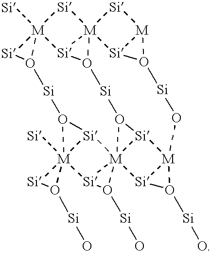
- FIG. 13 a side view (looking in the ⁇ 110 > direction) of the atomic configuration of the Si substrate 10 , interface 14 , and single crystal oxide (specifically a alkaline-earth-metal perovskite) layer 26 is shown.
- the configuration shown comprises, in relative sizes, for illustrative purposes, from larger to smaller, barium atoms 30 , silicon atoms 32 , oxygen atoms 34 , and titanium atoms 36 .
- the Si substrate 10 comprises only silicon atoms 32 .
- the interface 14 comprises metal atoms (which in the preferred embodiment are illustrated as barium atoms 30 ), silicon atoms 32 , and oxygen atoms 34 .
- the single crystal oxide layer 26 comprises barium atoms 30 , oxygen atoms 34 , and titanium atoms 36 .
- a top view of the interface along view line AA of FIG. 13, shows the arrangement of the barium, silicon, and oxygen atoms 30 , 32 , 34 .
- a top view along line AA of FIG. 13, shows the interface 14 and the top atomic layer 11 of the Si substrate 10 .
- a monolayer equals 6.8 ⁇ 10 ⁇ 14 atoms/cm 2 and an atomic layer is one atom thick.
- the interface 14 shown in the FIGs. comprises a single atomic layer, but could be more than one atomic layer, while the Si substrate 10 and the alkaline-earth-metal metal oxide layer may be many atomic layers. Note that in FIG. 13, only four atomic layers of the Si substrate 10 and only three atomic layers of the single crystal oxide layer 26 are shown.
- the interface 14 comprises a half monolayer of the alkaline-earth-metal, a half monolayer of silicon, and a monolayer of oxygen.
- Each barium atom 30 is substantially equally spaced from four of the silicon atoms 32 in the Si substrate 10 .
- the silicon atoms 32 in the interface 14 are substantially on a line and equally spaced between the alkaline-earth-metal atoms in the ⁇ 110 > direction.
- Each silicon atom 32 in the top layer of atoms in the Si substrate 10 is bonded to an oxygen atom 34 in the interface 14 and each silicon atom 32 in the interface 14 is bonded to two oxygen atoms 34 in the interface 14 .
- the interface 14 comprises rows of barium, silicon, and oxygen atoms 30 , 32 , 34 in a 2 ⁇ 1 configuration on a ( 001 ) surface of the Si substrate 10 , 1 ⁇ in the ⁇ 110 > direction and 2 ⁇ in the ⁇ 110 > direction.
- the interface 14 has a 2 ⁇ 1 reconstruction.
- a thin, crystalline interface 14 with silicon 10 has been described herein.
- the interface 14 may comprise a single atomic layer. Better transistor applications are achieved by the interface 14 being thin, in that the electrical coupling of the overlying oxide layers to the Si substrate is not compromised, and in that the interface 14 is more stable since the atoms will more likely maintain their crystalinity in processing.
Abstract
Description
Claims (36)


Priority Applications (6)
| Application Number | Priority Date | Filing Date | Title |
|---|---|---|---|
| US09/274,268 US6248459B1 (en) | 1999-03-22 | 1999-03-22 | Semiconductor structure having a crystalline alkaline earth metal oxide interface with silicon |
| JP2000065098A JP2000294553A (en) | 1999-03-22 | 2000-03-09 | Semiconductor structure equipped with crystalline alkaline earth metallic oxide interface having silicon |
| KR1020000012758A KR20000076850A (en) | 1999-03-22 | 2000-03-14 | Semiconductor structure having a crystalline alkaline earth metal oxide interface with silicon |
| TW089104672A TW493276B (en) | 1999-03-22 | 2000-03-15 | Semiconductor structure having a crystalline alkaline earth metal oxide interface with silicon |
| EP00106227A EP1043427A1 (en) | 1999-03-22 | 2000-03-22 | Semiconductor structure having a crystalline alkaline earth metal oxide interface between silicon and a single crystal oxide layer |
| SG200003969A SG101424A1 (en) | 1999-03-22 | 2000-07-17 | Semiconductors structure having a crystalline alkaline earth metal oxide interface with silicon |
Applications Claiming Priority (1)
| Application Number | Priority Date | Filing Date | Title |
|---|---|---|---|
| US09/274,268 US6248459B1 (en) | 1999-03-22 | 1999-03-22 | Semiconductor structure having a crystalline alkaline earth metal oxide interface with silicon |
Publications (1)
| Publication Number | Publication Date |
|---|---|
| US6248459B1 true US6248459B1 (en) | 2001-06-19 |
Family
ID=23047510
Family Applications (1)
| Application Number | Title | Priority Date | Filing Date |
|---|---|---|---|
| US09/274,268 Expired - Lifetime US6248459B1 (en) | 1999-03-22 | 1999-03-22 | Semiconductor structure having a crystalline alkaline earth metal oxide interface with silicon |
Country Status (5)
| Country | Link |
|---|---|
| US (1) | US6248459B1 (en) |
| EP (1) | EP1043427A1 (en) |
| JP (1) | JP2000294553A (en) |
| KR (1) | KR20000076850A (en) |
| TW (1) | TW493276B (en) |
Cited By (26)
| Publication number | Priority date | Publication date | Assignee | Title |
|---|---|---|---|---|
| SG91317A1 (en) * | 1999-12-17 | 2002-09-17 | Motorola Inc | Semiconductor structure having a crystalline alkaline earth metal silicon nitride/oxide interface with silicon |
| US20020167070A1 (en) * | 2000-06-30 | 2002-11-14 | Motorola, Inc. | Hybrid semiconductor structure and device |
| US6493497B1 (en) | 2000-09-26 | 2002-12-10 | Motorola, Inc. | Electro-optic structure and process for fabricating same |
| US6498358B1 (en) | 2001-07-20 | 2002-12-24 | Motorola, Inc. | Structure and method for fabricating an electro-optic system having an electrochromic diffraction grating |
| US6501973B1 (en) | 2000-06-30 | 2002-12-31 | Motorola, Inc. | Apparatus and method for measuring selected physical condition of an animate subject |
| US6501121B1 (en) | 2000-11-15 | 2002-12-31 | Motorola, Inc. | Semiconductor structure |
| US6521911B2 (en) * | 2000-07-20 | 2003-02-18 | North Carolina State University | High dielectric constant metal silicates formed by controlled metal-surface reactions |
| US6531740B2 (en) | 2001-07-17 | 2003-03-11 | Motorola, Inc. | Integrated impedance matching and stability network |
| US6555946B1 (en) | 2000-07-24 | 2003-04-29 | Motorola, Inc. | Acoustic wave device and process for forming the same |
| US6559471B2 (en) | 2000-12-08 | 2003-05-06 | Motorola, Inc. | Quantum well infrared photodetector and method for fabricating same |
| US6590236B1 (en) | 2000-07-24 | 2003-07-08 | Motorola, Inc. | Semiconductor structure for use with high-frequency signals |
| US6589856B2 (en) | 2001-08-06 | 2003-07-08 | Motorola, Inc. | Method and apparatus for controlling anti-phase domains in semiconductor structures and devices |
| US6638838B1 (en) | 2000-10-02 | 2003-10-28 | Motorola, Inc. | Semiconductor structure including a partially annealed layer and method of forming the same |
| US6639249B2 (en) | 2001-08-06 | 2003-10-28 | Motorola, Inc. | Structure and method for fabrication for a solid-state lighting device |
| US6646293B2 (en) | 2001-07-18 | 2003-11-11 | Motorola, Inc. | Structure for fabricating high electron mobility transistors utilizing the formation of complaint substrates |
| US6652989B2 (en) * | 1999-04-06 | 2003-11-25 | Ut-Battelle, Llc | Structure and method for controlling band offset and alignment at a crystalline oxide-on-semiconductor interface |
| US6667196B2 (en) | 2001-07-25 | 2003-12-23 | Motorola, Inc. | Method for real-time monitoring and controlling perovskite oxide film growth and semiconductor structure formed using the method |
| US6673646B2 (en) | 2001-02-28 | 2004-01-06 | Motorola, Inc. | Growth of compound semiconductor structures on patterned oxide films and process for fabricating same |
| US6673667B2 (en) | 2001-08-15 | 2004-01-06 | Motorola, Inc. | Method for manufacturing a substantially integral monolithic apparatus including a plurality of semiconductor materials |
| SG101423A1 (en) * | 1999-03-22 | 2004-01-30 | Motorola Inc | Method for fabricating a semiconductor structure having a crystalline alkaline earth metal oxide interface with silicon |
| SG101424A1 (en) * | 1999-03-22 | 2004-01-30 | Motorola Inc | Semiconductors structure having a crystalline alkaline earth metal oxide interface with silicon |
| US6693033B2 (en) | 2000-02-10 | 2004-02-17 | Motorola, Inc. | Method of removing an amorphous oxide from a monocrystalline surface |
| US6693298B2 (en) | 2001-07-20 | 2004-02-17 | Motorola, Inc. | Structure and method for fabricating epitaxial semiconductor on insulator (SOI) structures and devices utilizing the formation of a compliant substrate for materials used to form same |
| US6709989B2 (en) | 2001-06-21 | 2004-03-23 | Motorola, Inc. | Method for fabricating a semiconductor structure including a metal oxide interface with silicon |
| DE10303875B4 (en) * | 2003-01-31 | 2006-03-16 | Technische Universität Clausthal | Structure, in particular semiconductor structure, and method for producing a structure |
| SG165139A1 (en) * | 2000-07-17 | 2010-10-28 | Freescale Semiconductor Inc | Method of preparing crystalline alkaline earth metal oxides on a si substrate |
Families Citing this family (6)
| Publication number | Priority date | Publication date | Assignee | Title |
|---|---|---|---|---|
| TW468212B (en) * | 1999-10-25 | 2001-12-11 | Motorola Inc | Method for fabricating a semiconductor structure including a metal oxide interface with silicon |
| US6291319B1 (en) * | 1999-12-17 | 2001-09-18 | Motorola, Inc. | Method for fabricating a semiconductor structure having a stable crystalline interface with silicon |
| EP1176230A1 (en) * | 2000-07-26 | 2002-01-30 | Motorola, Inc. | Method of preparing crystalline alkaline earth metal oxides on an Si substrate |
| US6524651B2 (en) * | 2001-01-26 | 2003-02-25 | Battelle Memorial Institute | Oxidized film structure and method of making epitaxial metal oxide structure |
| KR20020064624A (en) * | 2001-02-02 | 2002-08-09 | 삼성전자 주식회사 | Dielectric layer for semiconductor device and method of fabricating the same |
| JP2008034563A (en) * | 2006-07-27 | 2008-02-14 | National Institute Of Advanced Industrial & Technology | Mis type semiconductor device |
Citations (13)
| Publication number | Priority date | Publication date | Assignee | Title |
|---|---|---|---|---|
| DE4120258A1 (en) | 1991-06-19 | 1992-12-24 | Siemens Ag | Epitaxial prodn. of high temp. superconducting layer on substrate - by sputtering intermediate metal oxide layer on substrate, and then depositing superconducting layer |
| US5225031A (en) | 1991-04-10 | 1993-07-06 | Martin Marietta Energy Systems, Inc. | Process for depositing an oxide epitaxially onto a silicon substrate and structures prepared with the process |
| US5372992A (en) * | 1989-11-07 | 1994-12-13 | Sumitomo Electric Industries, Ltd. | Superconducting thin film |
| US5393352A (en) | 1992-05-01 | 1995-02-28 | Texas Instruments Incorporated | Pb/Bi-containing high-dielectric constant oxides using a non-P/Bi-containing perovskite as a buffer layer |
| US5450812A (en) | 1993-07-30 | 1995-09-19 | Martin Marietta Energy Systems, Inc. | Process for growing a film epitaxially upon an oxide surface and structures formed with the process |
| US5482003A (en) | 1991-04-10 | 1996-01-09 | Martin Marietta Energy Systems, Inc. | Process for depositing epitaxial alkaline earth oxide onto a substrate and structures prepared with the process |
| US5514484A (en) | 1992-11-05 | 1996-05-07 | Fuji Xerox Co., Ltd. | Oriented ferroelectric thin film |
| US5661112A (en) * | 1987-07-24 | 1997-08-26 | Hatta; Shinichiro | Superconductor |
| JPH09315897A (en) | 1996-05-31 | 1997-12-09 | Sumitomo Electric Ind Ltd | Single crystal oxide thin film having rock crystal type crystal structure and its production |
| US5767543A (en) | 1996-09-16 | 1998-06-16 | Motorola, Inc. | Ferroelectric semiconductor device having a layered ferroelectric structure |
| US5814583A (en) * | 1987-07-06 | 1998-09-29 | Sumitomo Electric Industries, Ltd. | Superconducting thin film and a method for preparing the same |
| US5830270A (en) | 1996-08-05 | 1998-11-03 | Lockheed Martin Energy Systems, Inc. | CaTiO3 Interfacial template structure on semiconductor-based material and the growth of electroceramic thin-films in the perovskite class |
| US6022410A (en) * | 1998-09-01 | 2000-02-08 | Motorola, Inc. | Alkaline-earth metal silicides on silicon |
-
1999
- 1999-03-22 US US09/274,268 patent/US6248459B1/en not_active Expired - Lifetime
-
2000
- 2000-03-09 JP JP2000065098A patent/JP2000294553A/en active Pending
- 2000-03-14 KR KR1020000012758A patent/KR20000076850A/en not_active Application Discontinuation
- 2000-03-15 TW TW089104672A patent/TW493276B/en not_active IP Right Cessation
- 2000-03-22 EP EP00106227A patent/EP1043427A1/en not_active Withdrawn
Patent Citations (13)
| Publication number | Priority date | Publication date | Assignee | Title |
|---|---|---|---|---|
| US5814583A (en) * | 1987-07-06 | 1998-09-29 | Sumitomo Electric Industries, Ltd. | Superconducting thin film and a method for preparing the same |
| US5661112A (en) * | 1987-07-24 | 1997-08-26 | Hatta; Shinichiro | Superconductor |
| US5372992A (en) * | 1989-11-07 | 1994-12-13 | Sumitomo Electric Industries, Ltd. | Superconducting thin film |
| US5225031A (en) | 1991-04-10 | 1993-07-06 | Martin Marietta Energy Systems, Inc. | Process for depositing an oxide epitaxially onto a silicon substrate and structures prepared with the process |
| US5482003A (en) | 1991-04-10 | 1996-01-09 | Martin Marietta Energy Systems, Inc. | Process for depositing epitaxial alkaline earth oxide onto a substrate and structures prepared with the process |
| DE4120258A1 (en) | 1991-06-19 | 1992-12-24 | Siemens Ag | Epitaxial prodn. of high temp. superconducting layer on substrate - by sputtering intermediate metal oxide layer on substrate, and then depositing superconducting layer |
| US5393352A (en) | 1992-05-01 | 1995-02-28 | Texas Instruments Incorporated | Pb/Bi-containing high-dielectric constant oxides using a non-P/Bi-containing perovskite as a buffer layer |
| US5514484A (en) | 1992-11-05 | 1996-05-07 | Fuji Xerox Co., Ltd. | Oriented ferroelectric thin film |
| US5450812A (en) | 1993-07-30 | 1995-09-19 | Martin Marietta Energy Systems, Inc. | Process for growing a film epitaxially upon an oxide surface and structures formed with the process |
| JPH09315897A (en) | 1996-05-31 | 1997-12-09 | Sumitomo Electric Ind Ltd | Single crystal oxide thin film having rock crystal type crystal structure and its production |
| US5830270A (en) | 1996-08-05 | 1998-11-03 | Lockheed Martin Energy Systems, Inc. | CaTiO3 Interfacial template structure on semiconductor-based material and the growth of electroceramic thin-films in the perovskite class |
| US5767543A (en) | 1996-09-16 | 1998-06-16 | Motorola, Inc. | Ferroelectric semiconductor device having a layered ferroelectric structure |
| US6022410A (en) * | 1998-09-01 | 2000-02-08 | Motorola, Inc. | Alkaline-earth metal silicides on silicon |
Non-Patent Citations (18)
| Title |
|---|
| "A Preliminary Consideration of the Growth Behaviour of CeO2, SrTiO3 and SrVO3 films on Si Substrate", Hirotoshi Nagata, Thin Golid Films, 224(1993), pp. 1-3. |
| "A Proposal of Epitaxial Oxide Thin Film Structures for Future Oxide Elecronics", M. Suzuki et al., Materials Science and Engineering B41 (1996), pp. 166-173. |
| "BaSi2 and Thin Film Alkaline Earth Silicides on Silicon", R.A. McKee et al., Appl. Phys. Lett. 63 (20), Nov. 15, 1993, pp. 2818-2820. |
| "Crystalline Oxides on Silicon: The First Five Monolayers", R.A. McKee et al., Physical Review Letters, vol. 81, No. 14, pp. 3014-3017, Oct. 1998. |
| "Effects of Buffer Layers in Epitaxial Growth of SrTiO3 Thin Film on Si(100)", Osamu Nkagawara et al., J. Appl. Phys. (1995), pp. 7226-7230. |
| "Epitaxial Growth of SrTiO3 Films on Si(100) Substrates Using a Focused Electron Beam Evaporation Method", Hiroyuki Mori et al., Jpn. J. Appl. Phys., vol. 30 (1991), pp. 1415-1417. |
| "Growth of Crystalline SrTiO3 Films on Si Substrates Using Thin Fluoride Buffer Layers and Their Electrical Properties", Bum Ki Moon et al., Jpn. J. Appl. Phys., vol. 33 (1994), pp. 5911-5916. |
| "Heteroepitaxial Growth of CeO2(001) Films on Si(001) Substrates by Pulsed Laser Deposition in Ultrahigh Vacuum", Hirotoshi Nagata et al. Jpn. J. Appl. Phys. vol. 30 (1991), pp. 1136-1138. |
| "Heteroepitaxial Growth of SrO films on Si Substrates", Yuichi Kado et al., J. Appl. Phys. 61(6), 1987, pp.2398-2400. |
| "Heteroepitaxy of Dissimilar Materials", Materials Research Society Symposium Proceedings, vol. 221, pp. 29-34. |
| "Heteroepitaxy on Silicon: Fundamentals, Structure, and Devices", Materials Research Society Symposium Proceedings, vol. 116, pp. 369-374, Apr. 1988. |
| "Molecular Beam Epitaxy Growth of Epitaxial Barium Silicide, Barium Oxide, and Barium Titanate on Silicon", R.A. McKee et al., Oak Ridge National Laboratory, 1991 American Institute of Physics, pp. 782-784. |
| "Molecular Beam Epitaxy of SrTiO3 Films on Si(100)-2×1 with SrO Buffer Layer", Toyokazu Tambo et al., Jpn. J. Appl. Phys., vol. 37 (1998) pp. 4454-4459. |
| "Molecular Beam Epitaxy of SrTiO3 Films on Si(100)-2x1 with SrO Buffer Layer", Toyokazu Tambo et al., Jpn. J. Appl. Phys., vol. 37 (1998) pp. 4454-4459. |
| "Roles of Buffer Layers in Epitaxial Growth of SrTiO3 Films on Silicon Substrates", Bum Ki Moon et al., Jpn. J. Appl. Phys., vol. 33 (1994) pp. 1472-1477. |
| "Silicon Molecular Beam Epitaxy", Materials Research Society Symposium Proceedings, vol. 220, pp. 595-600, May 1991. |
| "Surface Structures and the Orthorhombic Transformation of Thin Film BaSi2 on Silicon", R. A. McKee et al., Mat. Res. Soc. Symp. Proc., vol. 221, pp. 131-1326, 1991. |
| "The MBE Growth and Optical Quality of BaTiO3 and SrTiO3 Thin Films on MgO", R.A. McKee et al., Mat. Res. Soc. Symp. Proc. vol. 341, pp. 309-314, Apr. 1994. |
Cited By (27)
| Publication number | Priority date | Publication date | Assignee | Title |
|---|---|---|---|---|
| SG101423A1 (en) * | 1999-03-22 | 2004-01-30 | Motorola Inc | Method for fabricating a semiconductor structure having a crystalline alkaline earth metal oxide interface with silicon |
| SG101424A1 (en) * | 1999-03-22 | 2004-01-30 | Motorola Inc | Semiconductors structure having a crystalline alkaline earth metal oxide interface with silicon |
| US6652989B2 (en) * | 1999-04-06 | 2003-11-25 | Ut-Battelle, Llc | Structure and method for controlling band offset and alignment at a crystalline oxide-on-semiconductor interface |
| US6479173B1 (en) * | 1999-12-17 | 2002-11-12 | Motorola, Inc. | Semiconductor structure having a crystalline alkaline earth metal silicon nitride/oxide interface with silicon |
| SG91317A1 (en) * | 1999-12-17 | 2002-09-17 | Motorola Inc | Semiconductor structure having a crystalline alkaline earth metal silicon nitride/oxide interface with silicon |
| US6693033B2 (en) | 2000-02-10 | 2004-02-17 | Motorola, Inc. | Method of removing an amorphous oxide from a monocrystalline surface |
| US6501973B1 (en) | 2000-06-30 | 2002-12-31 | Motorola, Inc. | Apparatus and method for measuring selected physical condition of an animate subject |
| US20020167070A1 (en) * | 2000-06-30 | 2002-11-14 | Motorola, Inc. | Hybrid semiconductor structure and device |
| SG165139A1 (en) * | 2000-07-17 | 2010-10-28 | Freescale Semiconductor Inc | Method of preparing crystalline alkaline earth metal oxides on a si substrate |
| US6521911B2 (en) * | 2000-07-20 | 2003-02-18 | North Carolina State University | High dielectric constant metal silicates formed by controlled metal-surface reactions |
| US6555946B1 (en) | 2000-07-24 | 2003-04-29 | Motorola, Inc. | Acoustic wave device and process for forming the same |
| US6590236B1 (en) | 2000-07-24 | 2003-07-08 | Motorola, Inc. | Semiconductor structure for use with high-frequency signals |
| US6493497B1 (en) | 2000-09-26 | 2002-12-10 | Motorola, Inc. | Electro-optic structure and process for fabricating same |
| US6638838B1 (en) | 2000-10-02 | 2003-10-28 | Motorola, Inc. | Semiconductor structure including a partially annealed layer and method of forming the same |
| US6501121B1 (en) | 2000-11-15 | 2002-12-31 | Motorola, Inc. | Semiconductor structure |
| US6559471B2 (en) | 2000-12-08 | 2003-05-06 | Motorola, Inc. | Quantum well infrared photodetector and method for fabricating same |
| US6673646B2 (en) | 2001-02-28 | 2004-01-06 | Motorola, Inc. | Growth of compound semiconductor structures on patterned oxide films and process for fabricating same |
| US6709989B2 (en) | 2001-06-21 | 2004-03-23 | Motorola, Inc. | Method for fabricating a semiconductor structure including a metal oxide interface with silicon |
| US6531740B2 (en) | 2001-07-17 | 2003-03-11 | Motorola, Inc. | Integrated impedance matching and stability network |
| US6646293B2 (en) | 2001-07-18 | 2003-11-11 | Motorola, Inc. | Structure for fabricating high electron mobility transistors utilizing the formation of complaint substrates |
| US6693298B2 (en) | 2001-07-20 | 2004-02-17 | Motorola, Inc. | Structure and method for fabricating epitaxial semiconductor on insulator (SOI) structures and devices utilizing the formation of a compliant substrate for materials used to form same |
| US6498358B1 (en) | 2001-07-20 | 2002-12-24 | Motorola, Inc. | Structure and method for fabricating an electro-optic system having an electrochromic diffraction grating |
| US6667196B2 (en) | 2001-07-25 | 2003-12-23 | Motorola, Inc. | Method for real-time monitoring and controlling perovskite oxide film growth and semiconductor structure formed using the method |
| US6639249B2 (en) | 2001-08-06 | 2003-10-28 | Motorola, Inc. | Structure and method for fabrication for a solid-state lighting device |
| US6589856B2 (en) | 2001-08-06 | 2003-07-08 | Motorola, Inc. | Method and apparatus for controlling anti-phase domains in semiconductor structures and devices |
| US6673667B2 (en) | 2001-08-15 | 2004-01-06 | Motorola, Inc. | Method for manufacturing a substantially integral monolithic apparatus including a plurality of semiconductor materials |
| DE10303875B4 (en) * | 2003-01-31 | 2006-03-16 | Technische Universität Clausthal | Structure, in particular semiconductor structure, and method for producing a structure |
Also Published As
| Publication number | Publication date |
|---|---|
| EP1043427A1 (en) | 2000-10-11 |
| TW493276B (en) | 2002-07-01 |
| KR20000076850A (en) | 2000-12-26 |
| JP2000294553A (en) | 2000-10-20 |
Similar Documents
| Publication | Publication Date | Title |
|---|---|---|
| US6248459B1 (en) | Semiconductor structure having a crystalline alkaline earth metal oxide interface with silicon | |
| US6241821B1 (en) | Method for fabricating a semiconductor structure having a crystalline alkaline earth metal oxide interface with silicon | |
| US6291319B1 (en) | Method for fabricating a semiconductor structure having a stable crystalline interface with silicon | |
| US6479173B1 (en) | Semiconductor structure having a crystalline alkaline earth metal silicon nitride/oxide interface with silicon | |
| US6270568B1 (en) | Method for fabricating a semiconductor structure with reduced leakage current density | |
| US6319730B1 (en) | Method of fabricating a semiconductor structure including a metal oxide interface | |
| US6224669B1 (en) | Method for fabricating a semiconductor structure having a crystalline alkaline earth metal oxide interface with silicon | |
| US6709989B2 (en) | Method for fabricating a semiconductor structure including a metal oxide interface with silicon | |
| US7364989B2 (en) | Strain control of epitaxial oxide films using virtual substrates | |
| US6113690A (en) | Method of preparing crystalline alkaline earth metal oxides on a Si substrate | |
| US6022410A (en) | Alkaline-earth metal silicides on silicon | |
| US20020146895A1 (en) | Method for fabricating a semiconductor structure including a metal oxide interface with silicon | |
| WO2002041378A2 (en) | Semiconductor structure and process for fabricating same | |
| JPH0927601A (en) | Manufacture of memory and ferroelectric memory | |
| US6482538B2 (en) | Microelectronic piezoelectric structure and method of forming the same | |
| JPH10182292A (en) | Oxide laminated structure and its production | |
| KR20030051820A (en) | Semiconductor structure having high dielectric constant material | |
| CN1217036C (en) | Method for preparing crystalline alkaline earth metal oxide on silicon substrate | |
| CN1140914C (en) | Method for mfg. semioconductor structure having crystalline alkaline earth metal oxide interface with silicon | |
| EP1176230A1 (en) | Method of preparing crystalline alkaline earth metal oxides on an Si substrate |
Legal Events
| Date | Code | Title | Description |
|---|---|---|---|
| AS | Assignment |
Owner name: MOTOROLA, INC., ILLINOIS Free format text: ASSIGNMENT OF ASSIGNORS INTEREST;ASSIGNORS:WANG, JUN;OOMS, WILLIAM JAY;HALLMARK, JERALD ALLEN;REEL/FRAME:009847/0086 Effective date: 19990319 |
|
| STCF | Information on status: patent grant |
Free format text: PATENTED CASE |
|
| CC | Certificate of correction | ||
| AS | Assignment |
Owner name: FREESCALE SEMICONDUCTOR, INC., TEXAS Free format text: ASSIGNMENT OF ASSIGNORS INTEREST;ASSIGNOR:MOTOROLA, INC.;REEL/FRAME:015698/0657 Effective date: 20040404 Owner name: FREESCALE SEMICONDUCTOR, INC.,TEXAS Free format text: ASSIGNMENT OF ASSIGNORS INTEREST;ASSIGNOR:MOTOROLA, INC.;REEL/FRAME:015698/0657 Effective date: 20040404 |
|
| FPAY | Fee payment |
Year of fee payment: 4 |
|
| AS | Assignment |
Owner name: FREESCALE SEMICONDUCTOR, INC., TEXAS Free format text: ASSIGNMENT OF ASSIGNORS INTEREST;ASSIGNOR:MOTOROLA, INC.;REEL/FRAME:015603/0299 Effective date: 20041210 |
|
| AS | Assignment |
Owner name: CITIBANK, N.A. AS COLLATERAL AGENT, NEW YORK Free format text: SECURITY AGREEMENT;ASSIGNORS:FREESCALE SEMICONDUCTOR, INC.;FREESCALE ACQUISITION CORPORATION;FREESCALE ACQUISITION HOLDINGS CORP.;AND OTHERS;REEL/FRAME:018855/0129 Effective date: 20061201 Owner name: CITIBANK, N.A. AS COLLATERAL AGENT,NEW YORK Free format text: SECURITY AGREEMENT;ASSIGNORS:FREESCALE SEMICONDUCTOR, INC.;FREESCALE ACQUISITION CORPORATION;FREESCALE ACQUISITION HOLDINGS CORP.;AND OTHERS;REEL/FRAME:018855/0129 Effective date: 20061201 |
|
| FEPP | Fee payment procedure |
Free format text: PAYOR NUMBER ASSIGNED (ORIGINAL EVENT CODE: ASPN); ENTITY STATUS OF PATENT OWNER: LARGE ENTITY Free format text: PAYER NUMBER DE-ASSIGNED (ORIGINAL EVENT CODE: RMPN); ENTITY STATUS OF PATENT OWNER: LARGE ENTITY |
|
| FPAY | Fee payment |
Year of fee payment: 8 |
|
| AS | Assignment |
Owner name: CITIBANK, N.A., AS COLLATERAL AGENT,NEW YORK Free format text: SECURITY AGREEMENT;ASSIGNOR:FREESCALE SEMICONDUCTOR, INC.;REEL/FRAME:024397/0001 Effective date: 20100413 Owner name: CITIBANK, N.A., AS COLLATERAL AGENT, NEW YORK Free format text: SECURITY AGREEMENT;ASSIGNOR:FREESCALE SEMICONDUCTOR, INC.;REEL/FRAME:024397/0001 Effective date: 20100413 |
|
| REMI | Maintenance fee reminder mailed | ||
| FPAY | Fee payment |
Year of fee payment: 12 |
|
| SULP | Surcharge for late payment |
Year of fee payment: 11 |
|
| AS | Assignment |
Owner name: ZOZO MANAGEMENT, LLC, DELAWARE Free format text: ASSIGNMENT OF ASSIGNORS INTEREST;ASSIGNOR:FREESCALE SEMICONDUCTOR, INC.;REEL/FRAME:034038/0946 Effective date: 20120629 |
|
| AS | Assignment |
Owner name: APPLE INC., CALIFORNIA Free format text: ASSIGNMENT OF ASSIGNORS INTEREST;ASSIGNOR:ZOZO MANAGEMENT, LLC;REEL/FRAME:034732/0019 Effective date: 20141219 |
|
| AS | Assignment |
Owner name: FREESCALE SEMICONDUCTOR, INC., TEXAS Free format text: PATENT RELEASE;ASSIGNOR:CITIBANK, N.A., AS COLLATERAL AGENT;REEL/FRAME:037356/0553 Effective date: 20151207 Owner name: FREESCALE SEMICONDUCTOR, INC., TEXAS Free format text: PATENT RELEASE;ASSIGNOR:CITIBANK, N.A., AS COLLATERAL AGENT;REEL/FRAME:037356/0143 Effective date: 20151207 Owner name: FREESCALE SEMICONDUCTOR, INC., TEXAS Free format text: PATENT RELEASE;ASSIGNOR:CITIBANK, N.A., AS COLLATERAL AGENT;REEL/FRAME:037354/0225 Effective date: 20151207 |