US6249012B1 - Light emitting semiconductor device using gallium nitride group compound - Google Patents

Light emitting semiconductor device using gallium nitride group compound Download PDF

Info

Publication number
US6249012B1
US6249012B1 US08/956,950 US95695097A US6249012B1 US 6249012 B1 US6249012 B1 US 6249012B1 US 95695097 A US95695097 A US 95695097A US 6249012 B1 US6249012 B1 US 6249012B1
Authority
US
United States
Prior art keywords
layer
light
flow rate
semiconductor device
emitting diode
Prior art date
Legal status (The legal status is an assumption and is not a legal conclusion. Google has not performed a legal analysis and makes no representation as to the accuracy of the status listed.)
Expired - Fee Related
Application number
US08/956,950
Inventor
Katsuhide Manabe
Akira Mabuchi
Hisaki Kato
Michinari Sassa
Norikatsu Koide
Shiro Yamazaki
Masafumi Hashimoto
Isamu Akasaki
Current Assignee (The listed assignees may be inaccurate. Google has not performed a legal analysis and makes no representation or warranty as to the accuracy of the list.)
Nagoya University NUC
Japan Science and Technology Agency
Toyoda Gosei Co Ltd
Original Assignee
Nagoya University NUC
Toyoda Gosei Co Ltd
Japan Science and Technology Corp
Priority date (The priority date is an assumption and is not a legal conclusion. Google has not performed a legal analysis and makes no representation as to the accuracy of the date listed.)
Filing date
Publication date
Priority claimed from JP5021290A external-priority patent/JP2681094B2/en
Priority claimed from JP5021090A external-priority patent/JP3193980B2/en
Priority claimed from JP5021190A external-priority patent/JP3193981B2/en
Priority claimed from JP5020990A external-priority patent/JP2623466B2/en
Priority claimed from US07/926,022 external-priority patent/US5278433A/en
Priority to US08/956,950 priority Critical patent/US6249012B1/en
Application filed by Nagoya University NUC, Toyoda Gosei Co Ltd, Japan Science and Technology Corp filed Critical Nagoya University NUC
Priority to US09/417,778 priority patent/US6593599B1/en
Assigned to TOYODA GOSEI CO., LTD., NAGOYA UNIVERSITY, JAPAN SCIENCE AND TECHNOLOGY CORPORATION reassignment TOYODA GOSEI CO., LTD. ASSIGNMENT OF ASSIGNORS INTEREST (SEE DOCUMENT FOR DETAILS). Assignors: KABUSHIKI KAISHA TOYOTA CHUO KENKYUSHO
Priority to US09/586,607 priority patent/US6362017B1/en
Priority to US09/677,787 priority patent/US6472689B1/en
Priority to US09/677,781 priority patent/US6830992B1/en
Priority to US09/677,789 priority patent/US6472690B1/en
Priority to US09/677,788 priority patent/US6607595B1/en
Publication of US6249012B1 publication Critical patent/US6249012B1/en
Application granted granted Critical
Priority to US10/052,347 priority patent/US6984536B2/en
Anticipated expiration legal-status Critical
Expired - Fee Related legal-status Critical Current

Links

Images

Classifications

    • HELECTRICITY
    • H01ELECTRIC ELEMENTS
    • H01LSEMICONDUCTOR DEVICES NOT COVERED BY CLASS H10
    • H01L33/00Semiconductor devices with at least one potential-jump barrier or surface barrier specially adapted for light emission; Processes or apparatus specially adapted for the manufacture or treatment thereof or of parts thereof; Details thereof
    • H01L33/02Semiconductor devices with at least one potential-jump barrier or surface barrier specially adapted for light emission; Processes or apparatus specially adapted for the manufacture or treatment thereof or of parts thereof; Details thereof characterised by the semiconductor bodies
    • H01L33/26Materials of the light emitting region
    • H01L33/30Materials of the light emitting region containing only elements of group III and group V of the periodic system
    • H01L33/32Materials of the light emitting region containing only elements of group III and group V of the periodic system containing nitrogen
    • HELECTRICITY
    • H01ELECTRIC ELEMENTS
    • H01LSEMICONDUCTOR DEVICES NOT COVERED BY CLASS H10
    • H01L33/00Semiconductor devices with at least one potential-jump barrier or surface barrier specially adapted for light emission; Processes or apparatus specially adapted for the manufacture or treatment thereof or of parts thereof; Details thereof
    • H01L33/005Processes
    • H01L33/0062Processes for devices with an active region comprising only III-V compounds
    • H01L33/0066Processes for devices with an active region comprising only III-V compounds with a substrate not being a III-V compound
    • H01L33/007Processes for devices with an active region comprising only III-V compounds with a substrate not being a III-V compound comprising nitride compounds
    • HELECTRICITY
    • H01ELECTRIC ELEMENTS
    • H01LSEMICONDUCTOR DEVICES NOT COVERED BY CLASS H10
    • H01L33/00Semiconductor devices with at least one potential-jump barrier or surface barrier specially adapted for light emission; Processes or apparatus specially adapted for the manufacture or treatment thereof or of parts thereof; Details thereof
    • H01L33/02Semiconductor devices with at least one potential-jump barrier or surface barrier specially adapted for light emission; Processes or apparatus specially adapted for the manufacture or treatment thereof or of parts thereof; Details thereof characterised by the semiconductor bodies
    • H01L33/025Physical imperfections, e.g. particular concentration or distribution of impurities

Definitions

  • the present invention relates to a light-emitting semiconductor device using gallium nitride group compound which emits a blue light.
  • GaN compound semiconductor can be made into a light-emitting semiconductor device, such as a light-emitting diode (LED), which emits a blue light.
  • a light-emitting semiconductor device such as a light-emitting diode (LED)
  • LED light-emitting diode
  • the GaN compound semiconductor attracts attention because of its high light-emitting efficiency resulting from direct transition and of its ability to emit a blue light which is one of three primary colors.
  • the light-emitting diode manufactured from the GaN compound semiconductor is composed of an n-layer and an i-layer grown thereon.
  • the n-layer of the GaN compound semiconductor with n-type conduction is directly grown on a surface of a sapphire substrate or grown on a buffer layer of aluminum nitride formed on the substrate.
  • the i-layer of insulating (i-type) GaN compound semiconductor doped with p-type impurities is grown on the n-layer. (See Japanese Patent Laid-open Nos. 119196/1987 and 188977/1988.)
  • the light-emitting diode of this structure has room for improvement in luminous intensity. In addition, it comprises no p-n junction but it is made by joining the i-layer and n-layer.
  • An electric property of the GaN compound semiconductor shows inherently n-type conduction even though it is not deliberately doped with n-type impurities, and unlike silicon and similar semiconductors, when it is doped with zinc of p-type impurities, the electric property shows not p-type conduction but insulation. Moreover, the production of n-type GaN involves many difficulties in controlling conductivity.
  • the present inventors established a technology for a vapor phase epitaxy of the GaN group semiconductor with organometal compound.
  • This technology enables a production of a gas-phase grown GaN layer of high purity.
  • this technology provides n-type GaN with high resistivity without doping with impurities, unlike the conventional technology which provides n-type GaN with low resistivity when no doping is performed.
  • the n-layer of low carrier concentration should preferably have a carrier concentration of 1 ⁇ 10 14 /cm 3 to 1 ⁇ 10 17 /cm 3 and have a thickness of 0.5 to 2 ⁇ m.
  • the carrier concentration is higher than 1 ⁇ 10 17 /cm 3
  • the luminous intensity of the light-emitting diode decreases.
  • the carrier concentration is lower than 1 ⁇ 10 14 /cm 3
  • the series resistance of the light-emitting diode increases, an amount of heat generated in the n-layer increases when a constant current is supplied to it.
  • the layer thickness is greater than 2 ⁇ m, since the series resistance of the light-emitting diode increases, the amount of heat generated in the n-layer increases when the constant current is supplied to it. In the case where the layer thickness is smaller than 0.5 ⁇ m, the luminous intensity of the light-emitting diode decreases.
  • the n + -layer of high carrier concentration should preferably contain a carrier concentration of 1 ⁇ 10 17 /cm 3 to 1 ⁇ 10 19 /cm 3 and have a thickness of 2-10 ⁇ m.
  • the carrier concentration is higher than 1 ⁇ 10 19 /cm 3
  • the n + -layer is poor in crystallinity.
  • the carrier concentration is lower than 1 ⁇ 10 17 /cm 3
  • the layer thickness is greater than 10 ⁇ m
  • the substrate of the light-emitting diode warps.
  • the layer thickness is smaller than 2 ⁇ m, since the series resistance of the light-emitting diode increases, the amount of heat generated in the n + -layer increases when the constant current is supplied to it.
  • the n-layer in double-layer structure including an n-layer of low carrier concentration and an n + -layer of high carrier concentration, the former being adjacent to the i-layer.
  • the n-layer as a whole has a low electric resistance owing to the n + -layer of high carrier concentration, and hence the light-emitting diode has low series resistance and generates less heat when a constant current is supplied to it.
  • the n-layer adjacent to the i-layer has a lower carrier concentration or higher purity so that it contains a smaller amount of impurity atoms which are deleterious to the emission of blue light from the light-emission region (i-layer and its vicinity). Due to the above-mentioned functions, the light-emitting diode of the present invention emits a blue light of higher intensity.
  • the i L -layer of low impurity concentration should preferably contain the impurities in concentration of 1 ⁇ 10 16 /cm 3 to 5 ⁇ 10 19 /cm 3 and have a thickness of 0.01 to 1 ⁇ m.
  • the impurity concentration is higher than 5 ⁇ 10 19 /cm 3 , since the series resistance of the light-emitting diode increases, an initial voltage to start emitting light increases.
  • the impurity concentration is lower than 1 ⁇ 10 16 /cm 3 , the semiconductor of the i L -layer shows n-type conduction.
  • the layer thickness is greater than 1 ⁇ m, since the series resistance of the light-emitting diode increases, the initial voltage to start emitting light at increases. In the case where the layer thickness is smaller than 0.01 ⁇ m, the light-emitting diode has the same structure as that of the conventional one.
  • the iH-layer of high impurity concentration should preferably contain the impurities in concentration of 1 ⁇ 10 19 /cm 3 to 5 ⁇ 10 20 /cm 3 and have a thickness of 0.02 to 0.3 ⁇ m.
  • the impurity concentration is higher than 5 ⁇ 10 2 /cm 3
  • the semiconductor of the i H -layer is poor in crystallinity.
  • the impurity concentration is lower than 1 ⁇ 10 19 /cm 3
  • the luminous intensity of the light-emitting diode decreases.
  • the layer thickness is greater than 0.3 ⁇ m, since the series resistance of the light-emitting diode increases, an initial voltage to start emitting light at increases.
  • the i-layer is subject to breakage.
  • the i-layer in double-layer structure including an i L -layer containing p-type impurities in comparatively low concentration and an i H -layer containing p-type impurities in comparatively high concentration, the former being adjacent to the n-layer.
  • this structure in which the i-layer adjacent to the n-layer is the i L -layer of low impurity concentration) enables electrons to be injected from the n-layer into the i H -layer of high impurity concentration without being trapped in the i L -layer and its vicinity.
  • this structure enables electrons to pass through the i L -layer of low impurity concentration, which is poor in luminous efficacy, adjacent to the n-layer, and to reach the i H -layer of high impurity concentration in which electrons emit light with a high efficiency.
  • the third feature of the present invention is a combination of the first feature (the n-layer of double layer structure) and the second feature (the i-layer of double layer structure). Therefore, the n-layer of low carrier concentration, the n + -layer of high carrier concentration, the i L -layer of low impurity concentration, and the i H -layer of high impurity concentration should correspond to the respective layers as the first and second features.
  • the carrier concentration and layer thickness are defined in the same manner as in the first and second features.
  • the third feature of the present invention it is possible to increase an intensity of blue light from the light-emitting diode by making the n-layer in double-layer structure including an n-layer of low carrier concentration and an n + -layer of high carrier concentration, the former being adjacent to the i-layer, and also by making the i-layer in double-layer structure including an i L -layer containing p-type impurities in comparatively low concentration and an i H -layer containing p-type impurities in comparatively high concentration, the former being adjacent to the n-layer.
  • the n-layer as a whole has a low electric resistance owing to the n + -layer of high carrier concentration, which makes it possible to apply an effective voltage to the junction between the i L -layer and n-layer of low carrier concentration. Having a low carrier concentration. the n-layer adjacent to the i L -layer does not permit non-light-emitting impurity atoms to diffuse into the i L -layer. In addition, this structure (in which the i-layer adjacent to the n-layer is the i L -layer of low impurity concentration) permits electrons to be injected from the n-layer into the i H -layer of high impurity concentration without being trapped in the i L -layer.
  • this structure permits electrons to pass through the i L -layer of low impurity concentration, which is poor in luminous efficacy, adjacent to the n-layer, and to reach the i H -layer of high impurity concentration in which electrons emit light with a high efficiency.
  • the light-emitting diode of the present invention has a much higher luminous efficacy than the one having the conventional simple i-n junction.
  • This method comprises a step of feeding a silicon-containing gas and other raw material gases together at a proper mixing ratio so that the conductivity of the compound semiconductor is desirably controlled.
  • the mixing ratio is adjusted such that silicon enters the layer of gallium nitride compound semiconductor grown by vapor phase epitaxy and functions as the donor therein.
  • the fifth feature of the present invention resides in a method for producing a light-emitting semiconductor device.
  • the method comprises two steps.
  • the vapor phase epitaxy is accomplished on a sapphire substrate having a buffer layer of aluminum nitride by feeding a silicon-containing gas and other raw material gases together at a proper mixing ratio.
  • the vapor phase epitaxy is accomplished on the n + -layer formed by the first step by feeding raw material gases excluding the silicon-containing gas.
  • the n-layer of double-layer structure can be produced by properly controlling the mixing ratio of a silicon-containing gas and other raw material gases.
  • FIG. 1 is a diagram showing a structure of a light-emitting diode shown as Example 1 of the present invention.
  • FIGS. 2 to 7 are sectional views illustrating processes for producing a light-emitting diode shown as to Example 1 of the present invention.
  • FIG. 8 is a diagram showing relationship between a carrier concentration of an n-layer of low carrier concentration and intensity or wavelength of emitted light with respect to a light-emitting diode shown as Example 1 of the present invention.
  • FIG. 9 is a diagram showing a structure of a light-emitting diode shown as Example 2 of the present invention.
  • FIGS. 10 to 15 are sectional views illustrating processes for producing a light-emitting diode shown as Example 2 of the present invention.
  • FIG. 16 is a diagram showing relationship between an impurity concentration of an i H -layer of high impurity concentration and intensity or wavelength of emitted light with respect to a light-emitting diode shown as Example 2 of the present invention.
  • FIG. 17 is a diagram showing a structure of a light emitting diode shown as Example 3 of the present invention.
  • FIGS. 18 to 23 are sectional views illustrating processes for producing a light-emitting diode shown as Example 3 of the present invention.
  • FIG. 24 is a diagram showing relationship between a carrier concentration of an n-layer of low carrier concentration and intensity or wavelength of emitted light with respect to a light-emitting diode shown as Example 3 of the present invention.
  • FIG. 25 is a diagram showing relationship between an impurity concentration of an i H -layer of high impurity concentration and intensity or wavelength of emitted light with respect to a light-emitting diode shown as Example 3 of the present invention.
  • FIG. 26 is a diagram showing the relationship between a flow rate of silane gas and electrical properties of an n-layer formed by vapor phase epitaxy in a process shown as Example 4 of the present invention.
  • FIG. 1 there is shown a light-emitting diode 10 which has a sapphire substrate 1 on which is formed a buffer layer of 500 ⁇ thick AlN.
  • the AlN assumes a wurtzite-type structure.
  • On the buffer layer 2 are consecutively formed an n + -layer 3 of high carrier concentration of 2.2 ⁇ m thick GaN and an n-layer 4 of low carrier concentration of 1.5 ⁇ m thick GaN.
  • An i-(insulating) layer 6 of 0.2 ⁇ m thick GaN is formed on the n-layer 4 .
  • Aluminum electrodes 7 and 8 are connected to the i-layer 6 and n + -layer 3 , respectively.
  • This light-emitting diode 10 was produced by metal organic vapor phase epitaxy in the following manner. (This process is referred to as MOVPE hereinafter.)
  • the gases employed in this process are NH 3 , H 2 (as carrier gas), trimethyl gallium (Ga(CH 3 ) 3 ) (TMG hereinafter), trimethyl aluminum (Al(CH 3 ) 3 ) (TMA hereinafter), silane (SiH 4 ), and diethyl zinc (DEZ hereinafter).
  • the sapphire substrate 1 underwent vapor phase etching at 1100° C. with H 2 flowing through the reaction chamber at a flow rate of 2 l/min under normal pressure.
  • the AlN buffer layer 2 (about 500 ⁇ thick) at 400° C. by supplying H 2 at a flow rate of 20 l/min, NH 3 at a flow rate of 10 l/min, and TMA at a flow rate of 1.8 ⁇ 10 ⁇ 5 mol/min.
  • n + -layer 3 of high carrier concentration (1.5 ⁇ 10 18 /cm 3 ) of 2.2 ⁇ m thick GaN by supplying H 2 at a flow rate of 20 l/min, NH 3 at a flow rate of 10 l/min, TMG at a flow rate of 1.7 ⁇ 10 ⁇ 4 mol/min, and silane (diluted to 0.86 ppm with H 2 ) at a flow rate of 200 ml/min, with the sapphire substrate 1 kept at 1150° C.
  • n + -layer 3 On the n + -layer 3 was formed the n-layer 4 of low carrier concentration (1 ⁇ 10 15 /cm 3 ) of 1.5 ⁇ m thick GaN by supplying H 2 at a flow rate of 20 l/min, NH 3 at a flow rate of 10 l/min, and TMG at a flow rate of 1.7 ⁇ 10 ⁇ 4 mol/min, with the sapphire substrate 1 kept at 1150° C.
  • n-layer 4 On the n-layer 4 was formed the i-layer 6 of 0.2 ⁇ m thick GaN by supplying H 2 at a flow rate of 20 l/min, NH 3 at a flow rate of 10 l/min, TMG at a flow rate of 1.7 ⁇ 10 ⁇ 4 mol/min, and DEZ at a flow rate of 1.5 ⁇ 10 ⁇ 4 mol/min, with the sapphire substrate 1 kept at 900° C.
  • a 2000 ⁇ thick SiO 2 layer 11 by sputtering as shown in FIG. 3 .
  • a photoresist layer 12 which subsequently underwent a photolithographic processing to make a pattern corresponding to a figure of the electrode connected to the n + -layer 3 .
  • the exposed part (not covered by the photoresist layer 12 ) of the SiO 2 layer 11 underwent etching with hydrofluoric acid for its removal, as shown in FIG. 4 .
  • the exposed part (not covered by the photoresist layer 12 and the SiO 2 layer 11 ) of the i-layer 6 underwent dry etching with CCl 2 F 2 gas at a flow rate of 10 cc/min and a high-frequency electric power of 0.44 W/cm 2 in a vacuum of 0.04 Torr and subsequently underwent dry etching with argon.
  • the dry etching removed not only the exposed part of the i-layer 6 but also the n-layer 4 and the upper part of the n + -layer 3 which are underneath the exposed part of the i-layer 6 , as shown in FIG. 5 .
  • the SiO 2 layer 11 remaining on the i-layer 6 was removed with hydrofluoric acid as shown in FIG. 6 .
  • an Al layer 13 by vapor deposition as shown in FIG. 7 .
  • a photoresist layer 14 which subsequently underwent the photolithographic processing to make a pattern corresponding to a figure of the electrodes connected to the n + -layer 3 and the i-layer 6 , respectively.
  • the exposed part (not covered by the photoresist layer 14 ) of the Al layer 13 underwent etching with nitric acid as shown in FIG. 7 .
  • the photoresist 14 was removed with acetone.
  • the electrode 8 for the n + -layer 3 and the electrode 7 for the i-layer 6 were formed.
  • Such an above-mentioned process could make a gallium nitride light-emitting element of MIS (metal-insulator-semiconductor) structure as shown in FIG. 1 .
  • MIS metal-insulator-semiconductor
  • the thus obtained light-emitting diode 10 was found to have a luminous intensity of 0.2 mcd. This value is 4 times higher than that of the conventional light-emitting diode which is composed simply of an i-layer with impurity concentration of 2 ⁇ 10 20 /cm 3 and a 4 ⁇ m thick n-layer with carrier concentration of 5 ⁇ 10 17 /cm 3 .
  • FIG. 9 there is shown a light-emitting diode 10 which has a sapphire substrate 1 on which is formed a 500 ⁇ thick AlN buffer layer 2 .
  • a 4 ⁇ m thick GaN n-layer 3 with carrier concentration of 5 ⁇ 10 17 /cm 3 , an i L -layer 5 of low impurity concentration of 5 ⁇ 10 19 /cm 3 of Zn, and an i H -layer 6 of high impurity concentration (2 ⁇ 10 20 /cm 3 of Zn).
  • aluminum electrodes 7 and 8 are connected to the i H -layer 6 and n-layer 3 , respectively.
  • This light-emitting diode 10 was produced by the MOVPE.
  • the gases employed in this process are NH 3 , H 2 (as carrier gas), trimethyl gallium TMG, trimethyl aluminum TMA, and diethyl zinc DEZ.
  • the sapphire substrate 1 underwent vapor phase etching at 1100° C. with H 2 flowing through the reaction chamber at a flow rate of 2 l/min under normal pressure.
  • the AlN buffer layer 2 (about 500 ⁇ thick) at 400° C. by supplying H 2 at a flow rate of 20 l/min, NH 3 at a flow rate of 10 l/min, and TMA at a flow rate of 1.8 ⁇ 10 ⁇ 5 mol/min.
  • the buffer layer 2 On the buffer layer 2 was formed the 4 ⁇ m thick GaN n-layer 3 with carrier concentration of 1.5 ⁇ 10 17 /cm 3 by supplying H 2 at a flow rate of 20 l/min, NH 3 at a flow rate of 10 l/min, and TMG at a flow rate of 1.7 ⁇ 10 ⁇ 4 mol/min with stopping the feeding of TMA, with the sapphire substrate 1 kept at 1150° C.
  • n-layer 3 On the n-layer 3 was formed the 0.2 ⁇ m thick GaN i L -layer 5 of low impurity concentration (5 ⁇ 10 19 /cm 3 of Zn) by supplying H 2 at a flow rate of 20 l/min, NH 3 at a flow rate of 10 l/min, TMG at a flow rate of 1.7 ⁇ 10 ⁇ 4 mol/min, and DEZ at a flow rate of 1.5 ⁇ 10 ⁇ 4 mol/min, with the sapphire substrate 1 kept at 1000° C.
  • the i L -layer 5 On the i L -layer 5 was formed the 0.2 ⁇ m thick GaN i H -layer 6 of high impurity concentration (2 ⁇ 10 20 /cm 3 of Zn) by supplying H 2 at a flow rate of 20 l/min, NH 3 at a flow rate of 10 l/min, TMG at a flow rate of 1.7 ⁇ 10 ⁇ 4 mol/min, and DEZ at a flow rate of 1.5 ⁇ 10 ⁇ 4 mol/min, with the sapphire substrate 1 kept at 900° C.
  • the i H -layer 6 On the i H -layer 6 was formed the 2000 ⁇ thick SiO 2 layer 11 by sputtering as shown in FIG. 11 . On the SiO 2 layer 11 was formed a photoresist layer 12 which subsequently underwent photolithographic processing to make a pattern corresponding to the figure of the electrode connected to the n-layer 3 .
  • the exposed part (not covered by the photoresist layer 12 ) of the SiO 2 layer 11 underwent etching with hydrofluoric acid for its removal, as shown in FIG. 12 .
  • the exposed part (not covered by the photoresist layer 12 and the SiO 2 layer 11 ) of the i H -layer 6 underwent dry etching with CCl 2 F 2 gas at a flow rate of 10 cc/min and a high-frequency electric power of 0.44 W/cm2 in a vacuum of 0.04 Torr and subsequently underwent dry etching with argon.
  • the dry etching removed not only the exposed part of the i H -layer 6 but also the i L -layer 5 and the upper part of the n-layer 3 which are underneath the exposed part of the i H -layer 6 , as shown in FIG. 13 .
  • the SiO 2 layer 11 remaining on the i H -layer 6 was removed with hydrofluoric acid as shown in FIG. 14 .
  • an Al layer 13 by vapor deposition as shown in FIG. 15 .
  • the photoresist layer 14 which subsequently underwent the photolithographic processing to make a pattern corresponding to the figure of the electrodes connected to the n-layer 3 and the i H layer 6 , respectively.
  • the exposed part (not covered by the photoresist layer 14 ) of the Al layer 13 underwent etching with nitric acid as shown in FIG. 15 .
  • the photoresist 14 was removed with acetone.
  • the electrode 8 for the n-layer 3 and the electrode 7 for the i H -layer 6 were formed.
  • Such an above-mentioned process could make a gallium nitride light-emitting element of MIS structure as shown in FIG. 9 .
  • the thus obtained light-emitting diode 10 was found to have a luminous intensity of 0.2 mcd. This value is 4 times higher than that of the conventional light-emitting diode which is composed simply of a 0.2 ⁇ m thick i-layer with impurity concentration of 2 ⁇ 10 20 /cm 3 and a 4 ⁇ m thick n-layer with carrier concentration of 5 ⁇ 10 17 /cm 3 .
  • FIG. 17 there is shown a light-emitting diode 10 which has a sapphire substrate 1 on which is formed a 500 ⁇ thick AlN buffer layer 2 .
  • a 2.2 ⁇ m thick GaN n + -layer 3 of high carrier concentration (1.5 ⁇ 10 18 /cm 3 )
  • a 1.5 ⁇ m thick GaN n-layer 4 of low carrier concentration (1 ⁇ 10 15 /cm 3 )
  • an i L -layer 5 of low impurity concentration 5 ⁇ 10 19 /cm 3 of Zn
  • an i H -layer 6 of high impurity concentration (2 ⁇ 10 20 /cm 3 of Zn).
  • This light-emitting diode 10 was produced by the MOVPE with an organometallic compound in the following manner.
  • the gases employed in this process are NH 3 , H 2 (as carrier gas), trimethyl gallium (Ga(CH 3 ) 3 ) (TMG), trimethyl aluminum (Al(CH 3 ) 3 ) (TMA), silane (SiH 4 ), and diethyl zinc (DEZ).
  • the sapphire substrate 1 underwent vapor phase etching at 1100° C. with H 2 flowing through the reaction chamber at a flow rate of 2 l/min under normal pressure.
  • the AlN buffer layer 2 (about 500 ⁇ thick) at 400° C. by supplying H 2 at a flow rate of 20 l/min, NH 3 at a flow rate of 10 l/min, and TMA at a flow rate of 1.8 ⁇ 10 ⁇ 5 mol/min.
  • the buffer layer 2 On the buffer layer 2 was formed the 2.2 ⁇ m thick GaN n + -layer 3 of high carrier concentration (1.5 ⁇ 10 18 /cm 3 ) by supplying H 2 at a flow rate of 20 l/min, NH 3 at a flow rate of 10 l/min, TMG at a flow rate of 1.7 ⁇ 10 ⁇ 4 mol/min, and silane (diluted to 0.86 ppm with H 2 ) at a flow rate of 200 ml/min for 30 minutes, with the sapphire substrate 1 kept at 1150° C.
  • high carrier concentration 1.5 ⁇ 10 18 /cm 3
  • n + -layer 3 On the n + -layer 3 was formed the 1.5 ⁇ m thick GaN n-layer 4 of low carrier concentration (1 ⁇ 10 15 /cm 3 ) by supplying H 2 at a flow rate of 20 l/min, NH 3 at a flow rate of 10 l/min, and TMG at a flow rate of 1.7 ⁇ 10 ⁇ 4 mol/min, with the sapphire substrate 1 kept at 1150° C.
  • n-layer 4 On the n-layer 4 was formed the 0.2 ⁇ m thick GaN i L -layer 5 of low impurity concentration (5 ⁇ 10 19 /cm 3 of Zn) by supplying H 2 at a flow rate of 20 l/min, NH 3 at a flow rate of 10 l/min, TMG at a flow rate of 1.7 ⁇ 10 ⁇ 4 mol/min, and DEZ at a flow rate of 1.5 ⁇ 10 ⁇ 4 mol/min, with the sapphire substrate 1 kept at 1000° C.
  • low impurity concentration 5 ⁇ 10 19 /cm 3 of Zn
  • the i L -layer 5 On the i L -layer 5 was formed the 0.2 ⁇ m thick GaN i H -layer 6 of high impurity concentration (2 ⁇ 10 20 /cm 3 of Zn) by supplying H 2 at a flow rate of 20 l/min, NH 3 at a flow rate of 10 l/min, TMG at a flow rate of 1.7 ⁇ 10 ⁇ 4 mol/min, and DEZ at a flow rate of 1.5 ⁇ 10 ⁇ 4 mol/min, with the sapphire substrate 1 kept at 900° C.
  • the i H -layer 6 On the i H -layer 6 was formed the 2000 ⁇ thick SiO 2 layer 11 by sputtering as shown in FIG. 19 . On the SiO 2 layer 11 was formed a photoresist layer 12 which subsequently underwent the photolithographic processing to make a pattern for the electrode connected to the n + -layer 3 .
  • the exposed part (not covered by the photoresist layer 12 ) of the SiO 2 layer 11 underwent etching with hydrofluoric acid for its removal, as shown in FIG. 20 .
  • the exposed part (not covered by the photoresist layer 12 and the SiO 2 layer 11 ) of the i H -layer 6 underwent dry etching with CCr 2 F 2 gas at a flow rate of 10 cc/min and a high-frequency electric power of 0.44 W/cm 2 in a vacuum of 0.04 Torr and subsequently underwent dry etching with argon.
  • the dry etching removed not only the exposed part of the i H -layer 6 but also the i L -layer 5 and the n-layer 4 and the upper part of the n + -layer 3 which are underneath the exposed part of the i H -layer 6 , as shown in FIG. 21 .
  • the SiO 2 layer 11 remaining on the i H -layer 6 was removed with hydrofluoric arid as shown in FIG. 22 .
  • an Al layer 13 by vapor deposition as shown in FIG. 23 .
  • the photoresist layer 14 which subsequently underwent the photolithographic processing to make a pattern for the electrodes connected to the n + -layer 3 and the i H -layer 6 , respectively.
  • the exposed part (not covered by the photoresist layer 14 ) of the Al layer 13 underwent etching with nitric acid as shown in FIG. 23 .
  • the photoresist 14 was removed with acetone.
  • the electrode 8 for the n + -layer 3 and the electrode 7 for the i H -layer 6 were formed.
  • Such an above-mentioned process could make a gallium nitride light-emitting element of MIS structure as shown in FIG. 17 .
  • the thus obtained light-emitting diode 10 was found to have a luminous intensity of 0.4 mcd. This value is 8 times higher than that of the conventional light-emitting diode which is composed simply of a 0.2 ⁇ m thick i-layer with impurity concentration of 2 ⁇ 10 20 /cm 3 and a 4 ⁇ m thick n-layer with a carrier concentration of 5 ⁇ 10 17 cm 3 .
  • a light-emitting diode 10 of the same structure as in Example 1 was prepared in the same manner as in Example 1 according to the steps shown in FIGS. 2 to 7 .
  • the resistivity of the n + -layer 3 was varied in the range of 3 ⁇ 10 ⁇ 1 ⁇ cm to 8 ⁇ 10 ⁇ 3 ⁇ cm by changing the conditions of the vapor phase epitaxy for the n + -layer 3 of high carrier concentration, as shown in FIG. 26 .
  • the vapor phase epitaxy was carried out by supplying H 2 at a flow rate of 20 l/min, NH 3 at a flow rate of 10 l/min, TMG-carrying H 2 at a flow rate of 100 cc/min, and H 2 -diluted silane (0.86 ppm) at a flow rate of 10 cc/min to 300 cc/min.
  • the TMG-carrying H 2 was prepared by bubbling H 2 in TMG cooled at ⁇ 15° C.
  • the resistivity of the n + -layer 3 was varied by changing the flow rate of silane, but it is also possible to achieve the same object by changing the flow rate of other raw material gases or by changing the mixing ratio of silane and other raw material gases.
  • silane was used as the Si dopant, but it can be replaced by an organosilicon compound such as tetraethylsilane (Si(C 2 H 5 ) 4 ) in a gaseous state prepared by bubbling with H 2 .
  • organosilicon compound such as tetraethylsilane (Si(C 2 H 5 ) 4 ) in a gaseous state prepared by bubbling with H 2 .
  • the process mentioned above permits one to prepare the n + -layer 3 of high carrier concentration and the n-layer 4 of low carrier concentration in such a manner that their resistivity can be controlled as desired.
  • the thus obtained light-emitting diode 10 was found to have a luminous intensity of 0.2 mcd. This value is 4 times higher than that of the conventional light-emitting diode which is composed simply of an i-layer and an n-layer. In addition, the inspection of the luminescent surface revealed that the number of luminescent points is much greater than that of the conventional light-emitting diode.

Landscapes

  • Engineering & Computer Science (AREA)
  • Manufacturing & Machinery (AREA)
  • Computer Hardware Design (AREA)
  • Microelectronics & Electronic Packaging (AREA)
  • Power Engineering (AREA)
  • Led Devices (AREA)

Abstract

A semiconductor device having an n-type layer of gallium nitride that is doped with silicon and has a resistively ranging from 3×10⁻¹ Ωcm to 8×10⁻³ Ωcm or a carrier concentration ranging from 6×10¹⁶/cm3 to 3×10¹⁸/cm3.

Description

This is a division of application Ser. No. 08/556,232, filed Nov. 9, 1995, now U.S. Pat. No. 5,733,796, which is a file-wrapper-continuation of U.S. Ser. No. 08/179,242, filed on Jan. 10, 1994, now abandoned, which was a divisional of U.S. Ser. No. 07/926,022, filed Aug. 7, 1992, now U.S. Pat. No. 5,278,433, which was a Rule 62 file-wrapper-continuation of U.S. Ser. No. 07/661,304, filed Feb. 27, 1991, now abandoned.
BACKGROUND OF THE INVENTION
1. Field of the Invention
The present invention relates to a light-emitting semiconductor device using gallium nitride group compound which emits a blue light.
2. Description of the Prior Art
It is known that GaN compound semiconductor can be made into a light-emitting semiconductor device, such as a light-emitting diode (LED), which emits a blue light. The GaN compound semiconductor attracts attention because of its high light-emitting efficiency resulting from direct transition and of its ability to emit a blue light which is one of three primary colors.
The light-emitting diode manufactured from the GaN compound semiconductor is composed of an n-layer and an i-layer grown thereon. The n-layer of the GaN compound semiconductor with n-type conduction is directly grown on a surface of a sapphire substrate or grown on a buffer layer of aluminum nitride formed on the substrate. The i-layer of insulating (i-type) GaN compound semiconductor doped with p-type impurities is grown on the n-layer. (See Japanese Patent Laid-open Nos. 119196/1987 and 188977/1988.) The light-emitting diode of this structure has room for improvement in luminous intensity. In addition, it comprises no p-n junction but it is made by joining the i-layer and n-layer.
An electric property of the GaN compound semiconductor shows inherently n-type conduction even though it is not deliberately doped with n-type impurities, and unlike silicon and similar semiconductors, when it is doped with zinc of p-type impurities, the electric property shows not p-type conduction but insulation. Moreover, the production of n-type GaN involves many difficulties in controlling conductivity.
SUMMARY OF THE INVENTION
It is the first object of the present invention to improve a luminous efficiency of a GaN group light-emitting diode.
It is the second object of the present invention to provide a new layer structure which improves a luminous efficiency of a GaN group light-emitting diode.
It is the third object of the present invention to provide a technology for production of n-type GaN group compound semiconductor in which conductivity is easily controlled.
After experience in the manufacture of the above-mentioned GaN light-emitting diode, the present inventors established a technology for a vapor phase epitaxy of the GaN group semiconductor with organometal compound. This technology enables a production of a gas-phase grown GaN layer of high purity. In other words, this technology provides n-type GaN with high resistivity without doping with impurities, unlike the conventional technology which provides n-type GaN with low resistivity when no doping is performed.
The First Feature of the Invention;
The first feature of the present invention resides in a light-emitting semiconductor device composed of an n-layer of n-type gallium nitride group compound semiconductor (AlxGa1−xN; inclusive of x=0) and an i-layer of insulating (i-type) gallium nitride compound semiconductor (AlxGa1−xN; inclusive of x=0) doped with p-type impurities, in which the n-layer is of double-layer structure including an n-layer of low carrier concentration and an n+-layer of high carrier concentration, the former being adjacent to the i-layer.
According to the present invention, the n-layer of low carrier concentration should preferably have a carrier concentration of 1×10¹⁴/cm3 to 1×10¹⁷/cm3 and have a thickness of 0.5 to 2 μm. In the case where the carrier concentration is higher than 1×10¹⁷/cm3, the luminous intensity of the light-emitting diode decreases. In the case where the carrier concentration is lower than 1×10¹⁴/cm3, since the series resistance of the light-emitting diode increases, an amount of heat generated in the n-layer increases when a constant current is supplied to it. In the case where the layer thickness is greater than 2 μm, since the series resistance of the light-emitting diode increases, the amount of heat generated in the n-layer increases when the constant current is supplied to it. In the case where the layer thickness is smaller than 0.5 μm, the luminous intensity of the light-emitting diode decreases.
In addition, the n+-layer of high carrier concentration should preferably contain a carrier concentration of 1×10¹⁷/cm3 to 1×10¹⁹/cm3 and have a thickness of 2-10 μm. In the case where the carrier concentration is higher than 1×10¹⁹/cm3, the n+-layer is poor in crystallinity. In case that the carrier concentration is lower than 1×10¹⁷/cm3, since the series resistance of the light-emitting diode increases, an amount of heat generated in the n+-layer increases when a constant current is supplied to it. In the case where the layer thickness is greater than 10 μm, the substrate of the light-emitting diode warps. In case that the layer thickness is smaller than 2 μm, since the series resistance of the light-emitting diode increases, the amount of heat generated in the n+-layer increases when the constant current is supplied to it.
In the first feature of the present invention, it is possible to increase an intensity of blue light emitted from the light-emitting diode by making the n-layer in double-layer structure including an n-layer of low carrier concentration and an n+-layer of high carrier concentration, the former being adjacent to the i-layer. In other words, the n-layer as a whole has a low electric resistance owing to the n+-layer of high carrier concentration, and hence the light-emitting diode has low series resistance and generates less heat when a constant current is supplied to it. The n-layer adjacent to the i-layer has a lower carrier concentration or higher purity so that it contains a smaller amount of impurity atoms which are deleterious to the emission of blue light from the light-emission region (i-layer and its vicinity). Due to the above-mentioned functions, the light-emitting diode of the present invention emits a blue light of higher intensity.
The Second Feature of the Invention
The second feature of the present invention resides in a light-emitting semiconductor device composed of an n-layer of n-type gallium nitride compound semiconductor (Alx Ga 1−xN; inclusive of x=0) and an i-layer of i-type gallium nitride compound semiconductor (AlxGa1−xN; inclusive of x=0) doped with p-type impurities, in which the i-layer is of double-layer structure including an iL-layer containing p-type impurities in comparatively low concentration and an iH-layer containing p-type impurities in comparatively high concentration, the former being adjacent to the n-layer.
According to the present invention, the iL-layer of low impurity concentration should preferably contain the impurities in concentration of 1×10¹⁶/cm3 to 5×10¹⁹/cm3 and have a thickness of 0.01 to 1 μm. In the case where the impurity concentration is higher than 5×10¹⁹/cm3, since the series resistance of the light-emitting diode increases, an initial voltage to start emitting light increases. In the case where the impurity concentration is lower than 1×10¹⁶/cm3, the semiconductor of the iL-layer shows n-type conduction. In the case where the layer thickness is greater than 1 μm, since the series resistance of the light-emitting diode increases, the initial voltage to start emitting light at increases. In the case where the layer thickness is smaller than 0.01 μm, the light-emitting diode has the same structure as that of the conventional one.
In addition, the iH-layer of high impurity concentration should preferably contain the impurities in concentration of 1×10¹⁹/cm3 to 5×10²⁰/cm3 and have a thickness of 0.02 to 0.3 μm. In the case where the impurity concentration is higher than 5×10²/cm3, the semiconductor of the iH-layer is poor in crystallinity. In the case where the impurity concentration is lower than 1×10¹⁹/cm3, the luminous intensity of the light-emitting diode decreases. In case that the layer thickness is greater than 0.3 μm, since the series resistance of the light-emitting diode increases, an initial voltage to start emitting light at increases. In case that the layer thickness is smaller than 0.02 μm, the i-layer is subject to breakage.
In the second feature of the present invention, it is possible to increase an intensity of blue light emitted from the light-emitting diode by making the i-layer in double-layer structure including an iL-layer containing p-type impurities in comparatively low concentration and an iH-layer containing p-type impurities in comparatively high concentration, the former being adjacent to the n-layer. In other words, this structure (in which the i-layer adjacent to the n-layer is the iL-layer of low impurity concentration) enables electrons to be injected from the n-layer into the iH-layer of high impurity concentration without being trapped in the iL-layer and its vicinity. Therefore, this structure enables electrons to pass through the iL-layer of low impurity concentration, which is poor in luminous efficacy, adjacent to the n-layer, and to reach the iH-layer of high impurity concentration in which electrons emit light with a high efficiency.
The Third Feature of the Invention
The third feature of the present invention resides in a light-emitting semiconductor device composed of an n-layer of n-type gallium nitride compound semiconductor (AlxGa1−xN; inclusive of x=0) and an i-layer of i-type gallium nitride compound semiconductor (AlxGa1−xN; inclusive of x=0) doped with p-type impurities, in which the n-layer is of double-layer structure including an n-layer of low carrier concentration and an n+-layer of high carrier concentration, the former being adjacent to the i-layer, and the i-layer is of double-layer structure including an iL-layer containing p-type impurities in comparatively low concentration and an iH-layer containing p-type impurities in comparatively high concentration, the former being adjacent to the n-layer.
The third feature of the present invention is a combination of the first feature (the n-layer of double layer structure) and the second feature (the i-layer of double layer structure). Therefore, the n-layer of low carrier concentration, the n+-layer of high carrier concentration, the iL-layer of low impurity concentration, and the iH-layer of high impurity concentration should correspond to the respective layers as the first and second features. The carrier concentration and layer thickness are defined in the same manner as in the first and second features.
In the third feature of the present invention, it is possible to increase an intensity of blue light from the light-emitting diode by making the n-layer in double-layer structure including an n-layer of low carrier concentration and an n+-layer of high carrier concentration, the former being adjacent to the i-layer, and also by making the i-layer in double-layer structure including an iL-layer containing p-type impurities in comparatively low concentration and an iH-layer containing p-type impurities in comparatively high concentration, the former being adjacent to the n-layer.
In other words, the n-layer as a whole has a low electric resistance owing to the n+-layer of high carrier concentration, which makes it possible to apply an effective voltage to the junction between the iL-layer and n-layer of low carrier concentration. Having a low carrier concentration. the n-layer adjacent to the iL-layer does not permit non-light-emitting impurity atoms to diffuse into the iL-layer. In addition, this structure (in which the i-layer adjacent to the n-layer is the iL-layer of low impurity concentration) permits electrons to be injected from the n-layer into the iH-layer of high impurity concentration without being trapped in the iL-layer. Therefore, this structure permits electrons to pass through the iL-layer of low impurity concentration, which is poor in luminous efficacy, adjacent to the n-layer, and to reach the iH-layer of high impurity concentration in which electrons emit light with a high efficiency.
For this reason, the light-emitting diode of the present invention has a much higher luminous efficacy than the one having the conventional simple i-n junction.
The Fourth Feature of the Invention
The fourth feature of the present invention resides in a method of producing an n-type gallium nitride compound semiconductor (AlxGa1−xN; inclusive of x=0) an organometallic compound by vapor phase epitaxy. This method comprises a step of feeding a silicon-containing gas and other raw material gases together at a proper mixing ratio so that the conductivity of the compound semiconductor is desirably controlled. The mixing ratio is adjusted such that silicon enters the layer of gallium nitride compound semiconductor grown by vapor phase epitaxy and functions as the donor therein. Thus it is possible to vary the conductivity of the n-type layer by adjusting the mixing ratio.
The Fifth Feature of the Invention
The fifth feature of the present invention resides in a method for producing a light-emitting semiconductor device. The method comprises two steps. The first step involves growing an n+-layer of high carrier concentration (which is an n-type gallium nitride compound semiconductor (AlxGa1−xN; inclusive of x=0) having a comparatively high conductivity) by vapor phase epitaxy an organometallic compound. The vapor phase epitaxy is accomplished on a sapphire substrate having a buffer layer of aluminum nitride by feeding a silicon-containing gas and other raw material gases together at a proper mixing ratio. The second step involves growing an n-layer of low carrier concentration (which is an n-type gallium nitride compound semiconductor (AlxGa1−xN; inclusive of x=0) having a comparatively low conductivity) by vapor phase epitaxy from an organometallic compound. The vapor phase epitaxy is accomplished on the n+-layer formed by the first step by feeding raw material gases excluding the silicon-containing gas. The n-layer of double-layer structure can be produced by properly controlling the mixing ratio of a silicon-containing gas and other raw material gases.
BRIEF DESCRIPTION OF THE DRAWINGS
FIG. 1 is a diagram showing a structure of a light-emitting diode shown as Example 1 of the present invention.
FIGS. 2 to 7 are sectional views illustrating processes for producing a light-emitting diode shown as to Example 1 of the present invention.
FIG. 8 is a diagram showing relationship between a carrier concentration of an n-layer of low carrier concentration and intensity or wavelength of emitted light with respect to a light-emitting diode shown as Example 1 of the present invention.
FIG. 9 is a diagram showing a structure of a light-emitting diode shown as Example 2 of the present invention.
FIGS. 10 to 15 are sectional views illustrating processes for producing a light-emitting diode shown as Example 2 of the present invention.
FIG. 16 is a diagram showing relationship between an impurity concentration of an iH-layer of high impurity concentration and intensity or wavelength of emitted light with respect to a light-emitting diode shown as Example 2 of the present invention.
FIG. 17 is a diagram showing a structure of a light emitting diode shown as Example 3 of the present invention.
FIGS. 18 to 23 are sectional views illustrating processes for producing a light-emitting diode shown as Example 3 of the present invention.
FIG. 24 is a diagram showing relationship between a carrier concentration of an n-layer of low carrier concentration and intensity or wavelength of emitted light with respect to a light-emitting diode shown as Example 3 of the present invention.
FIG. 25 is a diagram showing relationship between an impurity concentration of an iH-layer of high impurity concentration and intensity or wavelength of emitted light with respect to a light-emitting diode shown as Example 3 of the present invention.
FIG. 26 is a diagram showing the relationship between a flow rate of silane gas and electrical properties of an n-layer formed by vapor phase epitaxy in a process shown as Example 4 of the present invention.
DETAILED DESCRIPTION OF THE INVENTION
The invention will be described in more detail with reference to the following examples.
Example 1
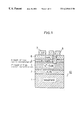
In FIG. 1 there is shown a light-emitting diode 10 which has a sapphire substrate 1 on which is formed a buffer layer of 500 Å thick AlN. As is know in the art, the AlN assumes a wurtzite-type structure. On the buffer layer 2 are consecutively formed an n+-layer 3 of high carrier concentration of 2.2 μm thick GaN and an n-layer 4 of low carrier concentration of 1.5 μm thick GaN. An i-(insulating) layer 6 of 0.2 μm thick GaN is formed on the n-layer 4. Aluminum electrodes 7 and 8 are connected to the i-layer 6 and n+-layer 3, respectively.
This light-emitting diode 10 was produced by metal organic vapor phase epitaxy in the following manner. (This process is referred to as MOVPE hereinafter.)
The gases employed in this process are NH3, H2 (as carrier gas), trimethyl gallium (Ga(CH3)3) (TMG hereinafter), trimethyl aluminum (Al(CH3)3) (TMA hereinafter), silane (SiH4), and diethyl zinc (DEZ hereinafter).
The sapphire substrate 1 of single crystal, with its principal crystal plane (a-surface {11{overscore (2)}0}) cleaned by solvent washing and heat treatment, was set on the susceptor placed in a reaction chamber of an MOVPE apparatus.
The sapphire substrate 1 underwent vapor phase etching at 1100° C. with H2 flowing through the reaction chamber at a flow rate of 2 l/min under normal pressure.
On the sapphire substrate 1 was formed the AlN buffer layer 2 (about 500 Å thick) at 400° C. by supplying H2 at a flow rate of 20 l/min, NH3 at a flow rate of 10 l/min, and TMA at a flow rate of 1.8×10⁻⁵ mol/min.
On the buffer layer 2 was formed the n+-layer 3 of high carrier concentration (1.5×10¹⁸/cm3) of 2.2 μm thick GaN by supplying H2 at a flow rate of 20 l/min, NH3 at a flow rate of 10 l/min, TMG at a flow rate of 1.7×10⁻⁴ mol/min, and silane (diluted to 0.86 ppm with H2) at a flow rate of 200 ml/min, with the sapphire substrate 1 kept at 1150° C.
On the n+-layer 3 was formed the n-layer 4 of low carrier concentration (1×10¹⁵/cm3) of 1.5 μm thick GaN by supplying H2 at a flow rate of 20 l/min, NH3 at a flow rate of 10 l/min, and TMG at a flow rate of 1.7×10⁻⁴ mol/min, with the sapphire substrate 1 kept at 1150° C.
On the n-layer 4 was formed the i-layer 6 of 0.2 μm thick GaN by supplying H2 at a flow rate of 20 l/min, NH3 at a flow rate of 10 l/min, TMG at a flow rate of 1.7×10⁻⁴ mol/min, and DEZ at a flow rate of 1.5×10⁻⁴ mol/min, with the sapphire substrate 1 kept at 900° C.
Thus there was obtained the multi-layer structure as shown in FIG. 2.
On the i-layer 6 was formed a 2000 Å thick SiO2 layer 11 by sputtering as shown in FIG. 3. On the SiO2 layer 11 was formed a photoresist layer 12 which subsequently underwent a photolithographic processing to make a pattern corresponding to a figure of the electrode connected to the n+-layer 3.
The exposed part (not covered by the photoresist layer 12) of the SiO2 layer 11 underwent etching with hydrofluoric acid for its removal, as shown in FIG. 4.
The exposed part (not covered by the photoresist layer 12 and the SiO2 layer 11) of the i-layer 6 underwent dry etching with CCl2F2 gas at a flow rate of 10 cc/min and a high-frequency electric power of 0.44 W/cm2 in a vacuum of 0.04 Torr and subsequently underwent dry etching with argon. The dry etching removed not only the exposed part of the i-layer 6 but also the n-layer 4 and the upper part of the n+-layer 3 which are underneath the exposed part of the i-layer 6, as shown in FIG. 5.
The SiO2 layer 11 remaining on the i-layer 6 was removed with hydrofluoric acid as shown in FIG. 6.
On the entire surface of the sample was formed an Al layer 13 by vapor deposition as shown in FIG. 7. On the Al layer 13 was formed a photoresist layer 14 which subsequently underwent the photolithographic processing to make a pattern corresponding to a figure of the electrodes connected to the n+-layer 3 and the i-layer 6, respectively.
The exposed part (not covered by the photoresist layer 14) of the Al layer 13 underwent etching with nitric acid as shown in FIG. 7. The photoresist 14 was removed with acetone. Thus there were formed the electrode 8 for the n+-layer 3 and the electrode 7 for the i-layer 6.
Such an above-mentioned process could make a gallium nitride light-emitting element of MIS (metal-insulator-semiconductor) structure as shown in FIG. 1.
The thus obtained light-emitting diode 10 was found to have a luminous intensity of 0.2 mcd. This value is 4 times higher than that of the conventional light-emitting diode which is composed simply of an i-layer with impurity concentration of 2×10²⁰/cm3 and a 4 μm thick n-layer with carrier concentration of 5×10¹⁷/cm3.
In addition, the inspection of the luminescent surface revealed that the number of luminescent points is much greater than that of the conventional light-emitting diode.
Several samples were prepared in the same manner as mentioned above except that the carrier concentration in the n-layer of low carrier concentration was varied, and they were tested for luminous intensity and emission spectrum. The results are shown in FIG. 8. It is noted that the luminous intensity decreases and the emission spectrum shifts to the red side according as the carrier concentration increases. This effect is estimated to be caused by atoms of silicon as doping atoms that diffuse or mix into the i-layer 6 as impurity atoms.
Example 2
In FIG. 9 there is shown a light-emitting diode 10 which has a sapphire substrate 1 on which is formed a 500 Å thick AlN buffer layer 2. On the buffer layer 2 are consecutively formed a 4 μm thick GaN n-layer 3 with carrier concentration of 5×10¹⁷/cm3, an iL-layer 5 of low impurity concentration of 5×10¹⁹/cm3 of Zn, and an iH-layer 6 of high impurity concentration (2×10²⁰/cm3 of Zn). To the iH-layer 6 and n-layer 3 are connected aluminum electrodes 7 and 8, respectively.
This light-emitting diode 10 was produced by the MOVPE.
The gases employed in this process are NH3, H2 (as carrier gas), trimethyl gallium TMG, trimethyl aluminum TMA, and diethyl zinc DEZ.
The sapphire substrate 1 of single crystal, with its principal crystal plane (c-surface {0001}) cleaned by solvent washing and heat treatment, was set on the susceptor placed in the reaction chamber of the MOVPE apparatus.
The sapphire substrate 1 underwent vapor phase etching at 1100° C. with H2 flowing through the reaction chamber at a flow rate of 2 l/min under normal pressure.
On the sapphire substrate 1 was formed the AlN buffer layer 2 (about 500 Å thick) at 400° C. by supplying H2 at a flow rate of 20 l/min, NH3 at a flow rate of 10 l/min, and TMA at a flow rate of 1.8×10⁻⁵ mol/min.
On the buffer layer 2 was formed the 4 μm thick GaN n-layer 3 with carrier concentration of 1.5×10¹⁷/cm3 by supplying H2 at a flow rate of 20 l/min, NH3 at a flow rate of 10 l/min, and TMG at a flow rate of 1.7×10⁻⁴ mol/min with stopping the feeding of TMA, with the sapphire substrate 1 kept at 1150° C.
On the n-layer 3 was formed the 0.2 μm thick GaN iL-layer 5 of low impurity concentration (5×10¹⁹/cm3 of Zn) by supplying H2 at a flow rate of 20 l/min, NH3 at a flow rate of 10 l/min, TMG at a flow rate of 1.7×10⁻⁴ mol/min, and DEZ at a flow rate of 1.5×10⁻⁴ mol/min, with the sapphire substrate 1 kept at 1000° C.
On the iL-layer 5 was formed the 0.2 μm thick GaN iH-layer 6 of high impurity concentration (2×10²⁰/cm3 of Zn) by supplying H2 at a flow rate of 20 l/min, NH3 at a flow rate of 10 l/min, TMG at a flow rate of 1.7×10⁻⁴ mol/min, and DEZ at a flow rate of 1.5×10⁻⁴ mol/min, with the sapphire substrate 1 kept at 900° C.
Thus there was obtained the multi-layer structure as shown in FIG. 10.
On the iH-layer 6 was formed the 2000 Å thick SiO2 layer 11 by sputtering as shown in FIG. 11. On the SiO2 layer 11 was formed a photoresist layer 12 which subsequently underwent photolithographic processing to make a pattern corresponding to the figure of the electrode connected to the n-layer 3.
The exposed part (not covered by the photoresist layer 12) of the SiO2 layer 11 underwent etching with hydrofluoric acid for its removal, as shown in FIG. 12.
The exposed part (not covered by the photoresist layer 12 and the SiO2 layer 11) of the iH-layer 6 underwent dry etching with CCl2F2 gas at a flow rate of 10 cc/min and a high-frequency electric power of 0.44 W/cm2 in a vacuum of 0.04 Torr and subsequently underwent dry etching with argon. The dry etching removed not only the exposed part of the iH-layer 6 but also the iL-layer 5 and the upper part of the n-layer 3 which are underneath the exposed part of the iH-layer 6, as shown in FIG. 13.
The SiO2 layer 11 remaining on the iH-layer 6 was removed with hydrofluoric acid as shown in FIG. 14.
On the entire surface of the sample was formed an Al layer 13 by vapor deposition as shown in FIG. 15. On the Al layer 13 was formed the photoresist layer 14 which subsequently underwent the photolithographic processing to make a pattern corresponding to the figure of the electrodes connected to the n-layer 3 and the iHlayer 6, respectively.
The exposed part (not covered by the photoresist layer 14) of the Al layer 13 underwent etching with nitric acid as shown in FIG. 15. The photoresist 14 was removed with acetone. Thus there were formed the electrode 8 for the n-layer 3 and the electrode 7 for the iH-layer 6.
Such an above-mentioned process could make a gallium nitride light-emitting element of MIS structure as shown in FIG. 9.
The thus obtained light-emitting diode 10 was found to have a luminous intensity of 0.2 mcd. This value is 4 times higher than that of the conventional light-emitting diode which is composed simply of a 0.2 μm thick i-layer with impurity concentration of 2×10²⁰/cm3 and a 4 μm thick n-layer with carrier concentration of 5×10¹⁷/cm3.
In addition, inspection of the luminescent surface revealed that the number of luminescent points is much greater than that of the conventional light-emitting diode.
Several samples were prepared in the same manner as mentioned above except that the impurity concentration in the iH-layer 6 of high impurity concentration was varied, and they were tested for luminous intensity and emission spectrum. The results are shown in FIG. 16. It is noted that the luminous intensity has a peak value and the emission spectrum shifts to a longer wavelength side when the impurity concentration increases.
Example 3
In FIG. 17 there is shown a light-emitting diode 10 which has a sapphire substrate 1 on which is formed a 500 Å thick AlN buffer layer 2. On the buffer layer 2 are consecutively formed a 2.2 μm thick GaN n+-layer 3 of high carrier concentration (1.5×10¹⁸/cm3), a 1.5 μm thick GaN n-layer 4 of low carrier concentration (1×10¹⁵/cm3), an iL-layer 5 of low impurity concentration (5×10¹⁹/cm3 of Zn), and an iH-layer 6 of high impurity concentration (2×10²⁰/cm3 of Zn). To the iH layer 6 and n+-layer 3 are connected aluminum electrodes 7 and 8, respectively. This light-emitting diode 10 was produced by the MOVPE with an organometallic compound in the following manner.
The gases employed in this process are NH3, H2 (as carrier gas), trimethyl gallium (Ga(CH3)3) (TMG), trimethyl aluminum (Al(CH3)3) (TMA), silane (SiH4), and diethyl zinc (DEZ).
The sapphire substrate 1 of single crystal, with its principal crystal plane (c-surface {0001}) cleaned by solvent washing and heat treatment, was set on the susceptor placed in the reaction chamber of the MOVPE apparatus.
The sapphire substrate 1 underwent vapor phase etching at 1100° C. with H2 flowing through the reaction chamber at a flow rate of 2 l/min under normal pressure.
On the sapphire substrate 1 was formed the AlN buffer layer 2 (about 500 Å thick) at 400° C. by supplying H2 at a flow rate of 20 l/min, NH3 at a flow rate of 10 l/min, and TMA at a flow rate of 1.8×10⁻⁵ mol/min.
On the buffer layer 2 was formed the 2.2 μm thick GaN n+-layer 3 of high carrier concentration (1.5×10¹⁸/cm3) by supplying H2 at a flow rate of 20 l/min, NH3 at a flow rate of 10 l/min, TMG at a flow rate of 1.7×10⁻⁴ mol/min, and silane (diluted to 0.86 ppm with H2) at a flow rate of 200 ml/min for 30 minutes, with the sapphire substrate 1 kept at 1150° C.
On the n+-layer 3 was formed the 1.5 μm thick GaN n-layer 4 of low carrier concentration (1×10¹⁵/cm3) by supplying H2 at a flow rate of 20 l/min, NH3 at a flow rate of 10 l/min, and TMG at a flow rate of 1.7×10⁻⁴ mol/min, with the sapphire substrate 1 kept at 1150° C.
On the n-layer 4 was formed the 0.2 μm thick GaN iL-layer 5 of low impurity concentration (5×10¹⁹/cm3 of Zn) by supplying H2 at a flow rate of 20 l/min, NH3 at a flow rate of 10 l/min, TMG at a flow rate of 1.7×10⁻⁴ mol/min, and DEZ at a flow rate of 1.5×10⁻⁴ mol/min, with the sapphire substrate 1 kept at 1000° C.
On the iL-layer 5 was formed the 0.2 μm thick GaN iH-layer 6 of high impurity concentration (2×10²⁰/cm3 of Zn) by supplying H2 at a flow rate of 20 l/min, NH3 at a flow rate of 10 l/min, TMG at a flow rate of 1.7×10⁻⁴ mol/min, and DEZ at a flow rate of 1.5×10⁻⁴ mol/min, with the sapphire substrate 1 kept at 900° C.
Thus there was obtained the multi-layer structure as shown in FIG. 18.
On the iH-layer 6 was formed the 2000 Å thick SiO2 layer 11 by sputtering as shown in FIG. 19. On the SiO2 layer 11 was formed a photoresist layer 12 which subsequently underwent the photolithographic processing to make a pattern for the electrode connected to the n+-layer 3.
The exposed part (not covered by the photoresist layer 12) of the SiO2 layer 11 underwent etching with hydrofluoric acid for its removal, as shown in FIG. 20.
The exposed part (not covered by the photoresist layer 12 and the SiO2 layer 11) of the iH-layer 6 underwent dry etching with CCr2F2 gas at a flow rate of 10 cc/min and a high-frequency electric power of 0.44 W/cm2 in a vacuum of 0.04 Torr and subsequently underwent dry etching with argon. The dry etching removed not only the exposed part of the iH-layer 6 but also the iL-layer 5 and the n-layer 4 and the upper part of the n+-layer 3 which are underneath the exposed part of the iH-layer 6, as shown in FIG. 21.
The SiO2 layer 11 remaining on the iH-layer 6 was removed with hydrofluoric arid as shown in FIG. 22.
On the entire surface of the sample was formed an Al layer 13 by vapor deposition as shown in FIG. 23. On the Al layer 13 was formed the photoresist layer 14 which subsequently underwent the photolithographic processing to make a pattern for the electrodes connected to the n+-layer 3 and the iH-layer 6, respectively.
The exposed part (not covered by the photoresist layer 14) of the Al layer 13 underwent etching with nitric acid as shown in FIG. 23. The photoresist 14 was removed with acetone. Thus there were formed the electrode 8 for the n+-layer 3 and the electrode 7 for the iH-layer 6.
Such an above-mentioned process could make a gallium nitride light-emitting element of MIS structure as shown in FIG. 17.
The thus obtained light-emitting diode 10 was found to have a luminous intensity of 0.4 mcd. This value is 8 times higher than that of the conventional light-emitting diode which is composed simply of a 0.2 μm thick i-layer with impurity concentration of 2×10²⁰/cm3 and a 4 μm thick n-layer with a carrier concentration of 5×1017cm3.
In addition, the inspection of the luminescent surface revealed that the number of luminescent points is much greater than that of the conventional light-emitting diode.
Several samples were prepared in the same manner as mentioned above except that the carrier concentration in the n-layer 4 of low carrier concentration was varied, and they were tested for luminous intensity and emission spectrum. The results are shown in FIG. 24. It is noted that the luminous intensity decreases and the emission spectrum shifts to the red side according as the carrier concentration increases.
Also, several samples were prepared in the same manner as mentioned above except that the impurity concentration in the iH-layer 6 of high impurity concentration was varied, and they were tested for luminous intensity and emission spectrum. The results are shown in FIG. 25. It is noted that the luminous intensity has a peak value and the emission spectrum shifts to a longer wavelength side when the impurity concentration increases.
Example 4
A light-emitting diode 10 of the same structure as in Example 1 was prepared in the same manner as in Example 1 according to the steps shown in FIGS. 2 to 7. The resistivity of the n+-layer 3 was varied in the range of 3×10⁻¹ Ωcm to 8×10⁻³ Ω cm by changing the conditions of the vapor phase epitaxy for the n+-layer 3 of high carrier concentration, as shown in FIG. 26. The vapor phase epitaxy was carried out by supplying H2 at a flow rate of 20 l/min, NH3 at a flow rate of 10 l/min, TMG-carrying H2 at a flow rate of 100 cc/min, and H2-diluted silane (0.86 ppm) at a flow rate of 10 cc/min to 300 cc/min. (The TMG-carrying H2 was prepared by bubbling H2 in TMG cooled at −15° C.)
In the above-mentioned case, the resistivity of the n+-layer 3 was varied by changing the flow rate of silane, but it is also possible to achieve the same object by changing the flow rate of other raw material gases or by changing the mixing ratio of silane and other raw material gases.
In this example, silane was used as the Si dopant, but it can be replaced by an organosilicon compound such as tetraethylsilane (Si(C2H5)4) in a gaseous state prepared by bubbling with H2.
The process mentioned above permits one to prepare the n+-layer 3 of high carrier concentration and the n-layer 4 of low carrier concentration in such a manner that their resistivity can be controlled as desired.
The thus obtained light-emitting diode 10 was found to have a luminous intensity of 0.2 mcd. This value is 4 times higher than that of the conventional light-emitting diode which is composed simply of an i-layer and an n-layer. In addition, the inspection of the luminescent surface revealed that the number of luminescent points is much greater than that of the conventional light-emitting diode.

Claims (9)

What is claimed is:
1. A semiconductor device comprising:
an n-type layer of a gallium nitride compound satisfies the formula that:
AlxGa1−xN; 0≦x≦1;
is doped with silicon (Si); and
has a resistivity ranging from 3×10⁻¹ Ωcm to 8×10⁻³ Ωcm.
2. A semiconductor device as claimed in claim 1, wherein said semiconductor device is a light-emitting device.
3. A semiconductor device as claimed in claim 1, further comprising a sapphire substrate over which said n-type layer is formed.
4. A semiconductor device as claimed in claim 3, further comprising a buffer layer between said sapphire substrate and said n-type layer.
5. A semiconductor device as claimed in claim 4, wherein said buffer layer is formed at a temperature lower than a temperature at which said n-type layer is formed.
6. A semiconductor device as claimed in claim 1, wherein said n-type layer comprises a gallium nitride compound.
7. A semiconductor device as claimed in claim 1, wherein said n-type layer is formed by organometallic compound vapor phase epitaxy.
8. A semiconductor device comprising:
an n-type layer of a gallium nitride compound that is doped with silicon at a predetermined doping rate and that has a resistivity not larger than 3×10⁻¹ Ωcm.
9. A semiconductor device comprising:
an n-type layer of a gallium nitride compound that is doped with silicon at a predetermined doping rate and that has a resistivity not larger than 3×10⁻¹ Ωcm and a carrier concentration not smaller than 6×10¹⁶/cm3.
US08/956,950 1990-02-28 1997-10-23 Light emitting semiconductor device using gallium nitride group compound Expired - Fee Related US6249012B1 (en)

Priority Applications (8)

Application Number Priority Date Filing Date Title
US08/956,950 US6249012B1 (en) 1990-02-28 1997-10-23 Light emitting semiconductor device using gallium nitride group compound
US09/417,778 US6593599B1 (en) 1990-02-28 1999-10-14 Light-emitting semiconductor device using gallium nitride group compound
US09/586,607 US6362017B1 (en) 1990-02-28 2000-06-02 Light-emitting semiconductor device using gallium nitride group compound
US09/677,788 US6607595B1 (en) 1990-02-28 2000-10-02 Method for producing a light-emitting semiconductor device
US09/677,789 US6472690B1 (en) 1990-02-28 2000-10-02 Gallium nitride group compound semiconductor
US09/677,781 US6830992B1 (en) 1990-02-28 2000-10-02 Method for manufacturing a gallium nitride group compound semiconductor
US09/677,787 US6472689B1 (en) 1990-02-28 2000-10-02 Light emitting device
US10/052,347 US6984536B2 (en) 1990-02-28 2002-01-23 Method for manufacturing a gallium nitride group compound semiconductor

Applications Claiming Priority (13)

Application Number Priority Date Filing Date Title
JP2-050212 1990-02-28
JP5021290A JP2681094B2 (en) 1990-02-28 1990-02-28 Gallium nitride based compound semiconductor light emitting device
JP5020990A JP2623466B2 (en) 1990-02-28 1990-02-28 Gallium nitride based compound semiconductor light emitting device
JP5021190A JP3193981B2 (en) 1990-02-28 1990-02-28 Gallium nitride based compound semiconductor light emitting device
JP2-050210 1990-02-28
JP2-050211 1990-02-28
JP5021090A JP3193980B2 (en) 1990-02-28 1990-02-28 Gallium nitride based compound semiconductor light emitting device
JP2-050209 1990-02-28
US66130491A 1991-02-27 1991-02-27
US07/926,022 US5278433A (en) 1990-02-28 1992-08-07 Light-emitting semiconductor device using gallium nitride group compound with double layer structures for the n-layer and/or the i-layer
US17924294A 1994-01-10 1994-01-10
US08/556,232 US5733796A (en) 1990-02-28 1995-11-09 Light-emitting semiconductor device using gallium nitride group compound
US08/956,950 US6249012B1 (en) 1990-02-28 1997-10-23 Light emitting semiconductor device using gallium nitride group compound

Related Parent Applications (2)

Application Number Title Priority Date Filing Date
US17924294A Continuation 1990-02-28 1994-01-10
US08/556,232 Division US5733796A (en) 1990-02-28 1995-11-09 Light-emitting semiconductor device using gallium nitride group compound

Related Child Applications (1)

Application Number Title Priority Date Filing Date
US09/417,778 Division US6593599B1 (en) 1990-02-28 1999-10-14 Light-emitting semiconductor device using gallium nitride group compound

Publications (1)

Publication Number Publication Date
US6249012B1 true US6249012B1 (en) 2001-06-19

Family

ID=27462459

Family Applications (4)

Application Number Title Priority Date Filing Date
US08/556,232 Expired - Lifetime US5733796A (en) 1990-02-28 1995-11-09 Light-emitting semiconductor device using gallium nitride group compound
US08/956,950 Expired - Fee Related US6249012B1 (en) 1990-02-28 1997-10-23 Light emitting semiconductor device using gallium nitride group compound
US09/417,778 Expired - Fee Related US6593599B1 (en) 1990-02-28 1999-10-14 Light-emitting semiconductor device using gallium nitride group compound
US09/677,788 Expired - Fee Related US6607595B1 (en) 1990-02-28 2000-10-02 Method for producing a light-emitting semiconductor device

Family Applications Before (1)

Application Number Title Priority Date Filing Date
US08/556,232 Expired - Lifetime US5733796A (en) 1990-02-28 1995-11-09 Light-emitting semiconductor device using gallium nitride group compound

Family Applications After (2)

Application Number Title Priority Date Filing Date
US09/417,778 Expired - Fee Related US6593599B1 (en) 1990-02-28 1999-10-14 Light-emitting semiconductor device using gallium nitride group compound
US09/677,788 Expired - Fee Related US6607595B1 (en) 1990-02-28 2000-10-02 Method for producing a light-emitting semiconductor device

Country Status (4)

Country Link
US (4) US5733796A (en)
EP (1) EP0444630B1 (en)
CA (1) CA2037198C (en)
DE (1) DE69126152T2 (en)

Cited By (10)

* Cited by examiner, † Cited by third party
Publication number Priority date Publication date Assignee Title
US20030160246A1 (en) * 2002-02-25 2003-08-28 Jagdish Narayan Efficient light emitting diodes and lasers
US20030199171A1 (en) * 2002-04-19 2003-10-23 Kopin Corporation Method for reducing the resistivity of p-type II-VI and III-V semiconductors
US20040000670A1 (en) * 2002-06-28 2004-01-01 Kopin Corporation Bonding pad for gallium nitride-based light-emitting device
US6734091B2 (en) 2002-06-28 2004-05-11 Kopin Corporation Electrode for p-type gallium nitride-based semiconductors
US6847052B2 (en) 2002-06-17 2005-01-25 Kopin Corporation Light-emitting diode device geometry
US20050040212A1 (en) * 2003-08-23 2005-02-24 Kuang-Neng Yang Method for manufacturing nitride light-emitting device
US20050179046A1 (en) * 2004-02-13 2005-08-18 Kopin Corporation P-type electrodes in gallium nitride-based light-emitting devices
US20050179042A1 (en) * 2004-02-13 2005-08-18 Kopin Corporation Monolithic integration and enhanced light extraction in gallium nitride-based light-emitting devices
US6955985B2 (en) 2002-06-28 2005-10-18 Kopin Corporation Domain epitaxy for thin film growth
US7122841B2 (en) 2003-06-04 2006-10-17 Kopin Corporation Bonding pad for gallium nitride-based light-emitting devices

Families Citing this family (49)

* Cited by examiner, † Cited by third party
Publication number Priority date Publication date Assignee Title
EP0444630B1 (en) * 1990-02-28 1997-05-21 Toyoda Gosei Co., Ltd. Light-emitting semiconductor device using gallium nitride group compound
US6362017B1 (en) * 1990-02-28 2002-03-26 Toyoda Gosei Co., Ltd. Light-emitting semiconductor device using gallium nitride group compound
US7235819B2 (en) * 1991-03-18 2007-06-26 The Trustees Of Boston University Semiconductor device having group III nitride buffer layer and growth layers
DE4313798A1 (en) * 1992-04-28 1993-11-04 Toyoda Gosei Kk Blue light emitting LED of gallium nitride semiconductor - has semi-insulating p=doped I-layer with double layer structure of low and high impurity concentration respectively.
DE69333250T2 (en) * 1992-07-23 2004-09-16 Toyoda Gosei Co., Ltd. Light emitting device made of a compound of the gallium nitride group
CN1132253C (en) * 1995-08-31 2003-12-24 株式会社东芝 Blue light emitting device and production method thereof
US5930656A (en) * 1996-10-21 1999-07-27 Kabushiki Kaisha Toshiba Method of fabricating a compound semiconductor device
JPH10294531A (en) * 1997-02-21 1998-11-04 Toshiba Corp Nitride compound semiconductor light emitting element
AU747260B2 (en) 1997-07-25 2002-05-09 Nichia Chemical Industries, Ltd. Nitride semiconductor device
JP3955367B2 (en) * 1997-09-30 2007-08-08 フィリップス ルミレッズ ライティング カンパニー リミテッド ライアビリティ カンパニー Optical semiconductor device and manufacturing method thereof
JP2000201050A (en) * 1998-11-02 2000-07-18 Ngk Insulators Ltd Substrate for surface acoustic wave device and manufacture of the same
US20010042866A1 (en) 1999-02-05 2001-11-22 Carrie Carter Coman Inxalygazn optical emitters fabricated via substrate removal
JP3770014B2 (en) 1999-02-09 2006-04-26 日亜化学工業株式会社 Nitride semiconductor device
EP1168539B1 (en) 1999-03-04 2009-12-16 Nichia Corporation Nitride semiconductor laser device
US6596079B1 (en) 2000-03-13 2003-07-22 Advanced Technology Materials, Inc. III-V nitride substrate boule and method of making and using the same
US6391748B1 (en) 2000-10-03 2002-05-21 Texas Tech University Method of epitaxial growth of high quality nitride layers on silicon substrates
JP3866540B2 (en) * 2001-07-06 2007-01-10 株式会社東芝 Nitride semiconductor device and manufacturing method thereof
JP3758537B2 (en) * 2001-07-23 2006-03-22 豊田合成株式会社 Method for producing group III nitride compound semiconductor
JP4342853B2 (en) * 2003-07-01 2009-10-14 独立行政法人科学技術振興機構 Method of growing nitride thin film on substrate and nitride thin film device
KR100486614B1 (en) * 2004-03-05 2005-05-03 에피밸리 주식회사 Ⅲ-Nitride compound semiconductor light emitting device with low contact resistance
KR100486177B1 (en) * 2004-03-25 2005-05-06 에피밸리 주식회사 Ⅲ-Nitride Compound Semiconductor Light Emitting Device
WO2006057485A1 (en) * 2004-11-29 2006-06-01 Epivalley Co., Ltd. Iii-nitride semiconductor light emitting device
US8168000B2 (en) * 2005-06-15 2012-05-01 International Rectifier Corporation III-nitride semiconductor device fabrication
KR100565894B1 (en) * 2005-07-06 2006-03-31 (주)룩셀런트 Method of controlling active layer of iii-nitride semiconductor light emitting device
KR101008285B1 (en) * 2005-10-28 2011-01-13 주식회사 에피밸리 ?-nitride semiconductor light emitting device
KR101008588B1 (en) * 2005-11-16 2011-01-17 주식회사 에피밸리 ?-nitride compound semiconductor light emitting device
WO2007119919A1 (en) * 2006-04-18 2007-10-25 Epivalley Co., Ltd. Iii-nitride semiconductor light emitting device and method for manufacturing the same
US20080315240A1 (en) * 2006-08-31 2008-12-25 Epivalley Co., Ltd. III-Nitride Semiconductor light Emitting Device
JP2008127252A (en) * 2006-11-22 2008-06-05 Hitachi Cable Ltd Nitride semiconductor ingot, nitride semiconductor substrate obtained from the same, and method for manufacturing nitride semiconductor ingot
KR20090034163A (en) * 2007-10-02 2009-04-07 주식회사 에피밸리 Iii-nitride semiconductor light emitting device
KR20090034169A (en) * 2007-10-02 2009-04-07 주식회사 에피밸리 Iii-nitride semiconductor light emitting device
KR100947676B1 (en) * 2007-12-17 2010-03-16 주식회사 에피밸리 ?-nitride semiconductor light emitting device
KR100972852B1 (en) * 2007-12-31 2010-07-28 주식회사 에피밸리 ?-nitride semiconductor light emitting device and method for manufacturing the same
KR20090073935A (en) * 2007-12-31 2009-07-03 주식회사 에피밸리 Iii-nitride semiconductor light emitting device
TWI362769B (en) * 2008-05-09 2012-04-21 Univ Nat Chiao Tung Light emitting device and fabrication method therefor
KR100941616B1 (en) * 2008-05-15 2010-02-11 주식회사 에피밸리 Semiconductor light emitting device
KR100988041B1 (en) * 2008-05-15 2010-10-18 주식회사 에피밸리 Semiconductor light emitting device
KR100997908B1 (en) * 2008-09-10 2010-12-02 박은현 ?-nitride semiconductor light emitting device
KR100981275B1 (en) * 2008-09-25 2010-09-10 주식회사 에피밸리 ?-nitride semiconductor light emitting device
KR101009651B1 (en) * 2008-10-15 2011-01-19 박은현 Iii-nitride semiconductor light emitting device
US20100102338A1 (en) * 2008-10-24 2010-04-29 Epivalley Co., Ltd. III-Nitride Semiconductor Light Emitting Device
US20100102352A1 (en) * 2008-10-24 2010-04-29 Epivalley Co., Ltd. III-Nitride Semiconductor Light Emitting Device
US8101965B2 (en) * 2008-12-02 2012-01-24 Epivalley Co., Ltd. III-nitride semiconductor light emitting device having a multilayered pad
KR100960280B1 (en) * 2008-12-02 2010-06-04 주식회사 에피밸리 Iii-nitride semiconductor light emitting device
US20100140656A1 (en) * 2008-12-04 2010-06-10 Epivalley Co., Ltd. Semiconductor Light-Emitting Device
KR101000276B1 (en) * 2008-12-04 2010-12-10 주식회사 에피밸리 Semiconductor light emiitting device
KR101134063B1 (en) * 2009-09-30 2012-04-13 주식회사 세미콘라이트 Iii-nitride semiconductor light emitting device
WO2011083551A1 (en) 2010-01-06 2011-07-14 パナソニック株式会社 Nitride semiconductor light-emitting element and process for production thereof
JP2012104528A (en) * 2010-11-08 2012-05-31 Sharp Corp Nitride semiconductor light-emitting element

Citations (39)

* Cited by examiner, † Cited by third party
Publication number Priority date Publication date Assignee Title
JPS4929771A (en) 1972-07-17 1974-03-16
JPS5042785A (en) 1973-08-20 1975-04-18
DE2738329A1 (en) 1976-09-06 1978-03-09 Philips Nv ELECTROLUMINESCENT GALLIUM NITRIDE SEMI-CONDUCTOR ARRANGEMENT AND METHOD OF MANUFACTURING IT
US4153905A (en) 1977-04-01 1979-05-08 Charmakadze Revaz A Semiconductor light-emitting device
JPS5471590A (en) 1977-11-17 1979-06-08 Matsushita Electric Ind Co Ltd Gan light emitting element and production of the same
JPS5471589A (en) 1977-11-17 1979-06-08 Matsushita Electric Ind Co Ltd Production of gan light emitting element
JPS5660076A (en) 1979-10-19 1981-05-23 Matsushita Electric Ind Co Ltd Gallium nitride light emitting element and manufacture thereof
DE3046018A1 (en) 1979-12-05 1981-09-03 Matsushita Electric Industrial Co., Ltd., 1006 Kadoma, Osaka ELECTROLUMINISCENCE SEMICONDUCTOR COMPONENT WITH GALLIUM NITRIDE AND METHOD FOR THE PRODUCTION THEREOF
JPS5746669A (en) 1980-09-03 1982-03-17 Japanese National Railways<Jnr> Stop position detector for linear motor
JPS5846686A (en) 1981-09-14 1983-03-18 Sanyo Electric Co Ltd Blue light emitting diode
US4396929A (en) 1979-10-19 1983-08-02 Matsushita Electric Industrial Company, Ltd. Gallium nitride light-emitting element and method of manufacturing the same
JPS59228776A (en) 1983-06-10 1984-12-22 Nippon Telegr & Teleph Corp <Ntt> Semiconductor hetero-junction element
JPS60173829A (en) 1984-02-14 1985-09-07 Nippon Telegr & Teleph Corp <Ntt> Growing method of compound semiconductor thin-film
US4608581A (en) 1982-02-02 1986-08-26 Bagratishvili Givi D Semiconductor light emitter based on gallium nitride and process for manufacture thereof
US4614961A (en) 1984-10-09 1986-09-30 Honeywell Inc. Tunable cut-off UV detector based on the aluminum gallium nitride material system
JPS62119196A (en) 1985-11-18 1987-05-30 Univ Nagoya Method for growing compound semiconductor
JPS63188977A (en) 1987-01-31 1988-08-04 Toyoda Gosei Co Ltd Light emitting element of gallium nitride compound semiconductor
EP0277597A2 (en) 1987-01-31 1988-08-10 Toyoda Gosei Co., Ltd. Gallium nitride group semiconductor light emitting diode and the process of producing the same
US4844989A (en) 1987-03-19 1989-07-04 The University Of Chicago (Arch Development Corp.) Superconducting structure with layers of niobium nitride and aluminum nitride
JPH0281483A (en) 1988-09-16 1990-03-22 Toyoda Gosei Co Ltd Gallium nitride-based compound semiconductor light-emitting element
JPH0281484A (en) 1988-09-16 1990-03-22 Toyoda Gosei Co Ltd Gallium nitride-based compound semiconductor light-emitting element
JPH0281482A (en) 1988-09-16 1990-03-22 Toyoda Gosei Co Ltd Gallium nitride-based compound semiconductor light-emitting element
US4911102A (en) 1987-01-31 1990-03-27 Toyoda Gosei Co., Ltd. Process of vapor growth of gallium nitride and its apparatus
US4945548A (en) 1988-04-28 1990-07-31 Digital Equipment Corporation Method and apparatus for detecting impending overflow and/or underrun of elasticity buffer
JPH02229475A (en) 1989-03-01 1990-09-12 Nippon Telegr & Teleph Corp <Ntt> Semiconductor light-emitting element
DE4006449A1 (en) 1989-03-01 1990-09-13 Toyoda Gosei Kk SUBSTRATE FOR GROWING A GALLIUM NITRIDE CONNECTION SEMICONDUCTOR DEVICE AND LIGHT EMITTER DIODE
JPH02275682A (en) 1989-01-13 1990-11-09 Toshiba Corp Compound semiconductor material and semiconductor element using same and manufacture thereof
JPH034549A (en) 1989-06-01 1991-01-10 Sumitomo Metal Ind Ltd Sample holding device
JPH0334549A (en) 1989-06-30 1991-02-14 Toshiba Corp Bipolar transistor
US5005057A (en) 1989-04-28 1991-04-02 Kabushiki Kaisha Toshiba Semiconductor light-emitting diode and method of manufacturing the same
US5006908A (en) 1989-02-13 1991-04-09 Nippon Telegraph And Telephone Corporation Epitaxial Wurtzite growth structure for semiconductor light-emitting device
US5076860A (en) 1989-01-13 1991-12-31 Kabushiki Kaisha Toshiba Algan compound semiconductor material
US5079184A (en) 1989-06-16 1992-01-07 Kabushiki Kaisha Toshiba Method of manufacturing iii-iv group compound semiconductor device
US5205905A (en) 1990-05-30 1993-04-27 Toyoda Gosei Co., Ltd. Dry etching method for semiconductor
US5218216A (en) 1987-01-31 1993-06-08 Toyoda Gosei Co., Ltd. Gallium nitride group semiconductor and light emitting diode comprising it and the process of producing the same
US5247533A (en) 1990-12-26 1993-09-21 Toyoda Gosei Co., Ltd. Gallium nitride group compound semiconductor laser diode
US5278433A (en) 1990-02-28 1994-01-11 Toyoda Gosei Co., Ltd. Light-emitting semiconductor device using gallium nitride group compound with double layer structures for the n-layer and/or the i-layer
EP0620203A1 (en) 1993-02-05 1994-10-19 Sumitomo Electric Industries, Ltd. Aluminum nitride sintered body and method of producing the same
JP3034549B2 (en) 1990-02-28 2000-04-17 ティーディーケイ株式会社 Magnetic toner for electrophotography, method for producing magnetic toner for electrophotography, and image forming method

Family Cites Families (15)

* Cited by examiner, † Cited by third party
Publication number Priority date Publication date Assignee Title
JPS6026079B2 (en) 1979-10-17 1985-06-21 松下電器産業株式会社 How to grow gallium nitride
JPS5718377A (en) * 1980-07-08 1982-01-30 Matsushita Electric Ind Co Ltd Light emitting element
JPS5787184A (en) * 1980-11-19 1982-05-31 Sanyo Electric Co Ltd Gan blue light emitting element
JPS57153479A (en) * 1981-03-17 1982-09-22 Matsushita Electric Ind Co Ltd Nitride gallium light emitting element
JPS5812381A (en) * 1981-07-16 1983-01-24 Sanyo Electric Co Ltd Gan blue light emitting element
JPS58200527A (en) 1982-05-18 1983-11-22 Oki Electric Ind Co Ltd Preparation of compound semiconductor thin film
JPS6095919A (en) * 1983-10-31 1985-05-29 Toshiba Corp Semiconductor element and manufacture thereof
JPS60175468A (en) 1984-02-21 1985-09-09 Matsushita Electric Ind Co Ltd Manufacture of gallium nitride semiconductor device
JPS617671A (en) * 1984-06-21 1986-01-14 Matsushita Electric Ind Co Ltd Gallium nitride semiconductor device
JPS63188938A (en) 1987-01-31 1988-08-04 Toyoda Gosei Co Ltd Method for vapor growth of gallium nitride compound semiconductor
US4946548A (en) * 1988-04-29 1990-08-07 Toyoda Gosei Co., Ltd. Dry etching method for semiconductor
JP2829311B2 (en) 1988-08-01 1998-11-25 豊田合成株式会社 Light emitting device manufacturing method
JP2809691B2 (en) * 1989-04-28 1998-10-15 株式会社東芝 Semiconductor laser
JP2623466B2 (en) 1990-02-28 1997-06-25 豊田合成株式会社 Gallium nitride based compound semiconductor light emitting device
EP0444630B1 (en) * 1990-02-28 1997-05-21 Toyoda Gosei Co., Ltd. Light-emitting semiconductor device using gallium nitride group compound

Patent Citations (45)

* Cited by examiner, † Cited by third party
Publication number Priority date Publication date Assignee Title
JPS4929771A (en) 1972-07-17 1974-03-16
JPS5042785A (en) 1973-08-20 1975-04-18
DE2738329A1 (en) 1976-09-06 1978-03-09 Philips Nv ELECTROLUMINESCENT GALLIUM NITRIDE SEMI-CONDUCTOR ARRANGEMENT AND METHOD OF MANUFACTURING IT
GB1589351A (en) 1976-09-06 1981-05-13 Philips Nv Electroluminescent device manufacture
US4268842A (en) 1976-09-06 1981-05-19 U.S. Philips Corporation Electroluminescent gallium nitride semiconductor device
US4153905A (en) 1977-04-01 1979-05-08 Charmakadze Revaz A Semiconductor light-emitting device
JPS5471590A (en) 1977-11-17 1979-06-08 Matsushita Electric Ind Co Ltd Gan light emitting element and production of the same
JPS5471589A (en) 1977-11-17 1979-06-08 Matsushita Electric Ind Co Ltd Production of gan light emitting element
US4396929A (en) 1979-10-19 1983-08-02 Matsushita Electric Industrial Company, Ltd. Gallium nitride light-emitting element and method of manufacturing the same
JPS5660076A (en) 1979-10-19 1981-05-23 Matsushita Electric Ind Co Ltd Gallium nitride light emitting element and manufacture thereof
DE3046018A1 (en) 1979-12-05 1981-09-03 Matsushita Electric Industrial Co., Ltd., 1006 Kadoma, Osaka ELECTROLUMINISCENCE SEMICONDUCTOR COMPONENT WITH GALLIUM NITRIDE AND METHOD FOR THE PRODUCTION THEREOF
US4408217A (en) 1979-12-05 1983-10-04 Matsushita Electric Industrial Company, Limited GaN Electroluminescent semiconductor device and method for making the same
US4473938A (en) 1979-12-05 1984-10-02 Matsushita Electric Industrial Co., Limited Method for making a GaN electroluminescent semiconductor device utilizing epitaxial deposition
JPS5746669A (en) 1980-09-03 1982-03-17 Japanese National Railways<Jnr> Stop position detector for linear motor
JPS5846686A (en) 1981-09-14 1983-03-18 Sanyo Electric Co Ltd Blue light emitting diode
US4608581A (en) 1982-02-02 1986-08-26 Bagratishvili Givi D Semiconductor light emitter based on gallium nitride and process for manufacture thereof
JPS59228776A (en) 1983-06-10 1984-12-22 Nippon Telegr & Teleph Corp <Ntt> Semiconductor hetero-junction element
JPS60173829A (en) 1984-02-14 1985-09-07 Nippon Telegr & Teleph Corp <Ntt> Growing method of compound semiconductor thin-film
US4614961A (en) 1984-10-09 1986-09-30 Honeywell Inc. Tunable cut-off UV detector based on the aluminum gallium nitride material system
JPS62119196A (en) 1985-11-18 1987-05-30 Univ Nagoya Method for growing compound semiconductor
US4855249A (en) 1985-11-18 1989-08-08 Nagoya University Process for growing III-V compound semiconductors on sapphire using a buffer layer
JPS63188977A (en) 1987-01-31 1988-08-04 Toyoda Gosei Co Ltd Light emitting element of gallium nitride compound semiconductor
EP0277597A2 (en) 1987-01-31 1988-08-10 Toyoda Gosei Co., Ltd. Gallium nitride group semiconductor light emitting diode and the process of producing the same
US4911102A (en) 1987-01-31 1990-03-27 Toyoda Gosei Co., Ltd. Process of vapor growth of gallium nitride and its apparatus
US5218216A (en) 1987-01-31 1993-06-08 Toyoda Gosei Co., Ltd. Gallium nitride group semiconductor and light emitting diode comprising it and the process of producing the same
US4844989A (en) 1987-03-19 1989-07-04 The University Of Chicago (Arch Development Corp.) Superconducting structure with layers of niobium nitride and aluminum nitride
US4945548A (en) 1988-04-28 1990-07-31 Digital Equipment Corporation Method and apparatus for detecting impending overflow and/or underrun of elasticity buffer
JPH0281484A (en) 1988-09-16 1990-03-22 Toyoda Gosei Co Ltd Gallium nitride-based compound semiconductor light-emitting element
JPH0281483A (en) 1988-09-16 1990-03-22 Toyoda Gosei Co Ltd Gallium nitride-based compound semiconductor light-emitting element
JPH0281482A (en) 1988-09-16 1990-03-22 Toyoda Gosei Co Ltd Gallium nitride-based compound semiconductor light-emitting element
JPH02275682A (en) 1989-01-13 1990-11-09 Toshiba Corp Compound semiconductor material and semiconductor element using same and manufacture thereof
US5076860A (en) 1989-01-13 1991-12-31 Kabushiki Kaisha Toshiba Algan compound semiconductor material
US5006908A (en) 1989-02-13 1991-04-09 Nippon Telegraph And Telephone Corporation Epitaxial Wurtzite growth structure for semiconductor light-emitting device
US5122845A (en) 1989-03-01 1992-06-16 Toyoda Gosei Co., Ltd. Substrate for growing gallium nitride compound-semiconductor device and light emitting diode
DE4006449A1 (en) 1989-03-01 1990-09-13 Toyoda Gosei Kk SUBSTRATE FOR GROWING A GALLIUM NITRIDE CONNECTION SEMICONDUCTOR DEVICE AND LIGHT EMITTER DIODE
JPH02229475A (en) 1989-03-01 1990-09-12 Nippon Telegr & Teleph Corp <Ntt> Semiconductor light-emitting element
US5005057A (en) 1989-04-28 1991-04-02 Kabushiki Kaisha Toshiba Semiconductor light-emitting diode and method of manufacturing the same
JPH034549A (en) 1989-06-01 1991-01-10 Sumitomo Metal Ind Ltd Sample holding device
US5079184A (en) 1989-06-16 1992-01-07 Kabushiki Kaisha Toshiba Method of manufacturing iii-iv group compound semiconductor device
JPH0334549A (en) 1989-06-30 1991-02-14 Toshiba Corp Bipolar transistor
US5278433A (en) 1990-02-28 1994-01-11 Toyoda Gosei Co., Ltd. Light-emitting semiconductor device using gallium nitride group compound with double layer structures for the n-layer and/or the i-layer
JP3034549B2 (en) 1990-02-28 2000-04-17 ティーディーケイ株式会社 Magnetic toner for electrophotography, method for producing magnetic toner for electrophotography, and image forming method
US5205905A (en) 1990-05-30 1993-04-27 Toyoda Gosei Co., Ltd. Dry etching method for semiconductor
US5247533A (en) 1990-12-26 1993-09-21 Toyoda Gosei Co., Ltd. Gallium nitride group compound semiconductor laser diode
EP0620203A1 (en) 1993-02-05 1994-10-19 Sumitomo Electric Industries, Ltd. Aluminum nitride sintered body and method of producing the same

Non-Patent Citations (29)

* Cited by examiner, † Cited by third party
Title
A.S. Grove, Physics and Technology of Semiconductor, Chpt, 4: Basics of Semiconductor Physics, 1967, translated and published in Japan Jun. 23, 1995, pp. 112-123.
Akasaki et al, Effects of AIN Buffer Layer on Crystallographic Structure and on Electrical and Optical Properties of GaN and Ga1xAlxN(0<x<0.4) Films Grown on Sapphire Substrate by MOVPE, Journal of Crystal Growth 98 (1989), pp. 209-219.
Akasaki et al., "High efficiency blue LED utilizing GaN utilizing GaN film with AIN buffer layer grown by MOVPE", Inst. Phys. Conf. Ser. No. 91: Chapter 7, GaAs and Related Compounds 1987, pp. 633-636, 1987.
Amano et al, Effects of the Buffer Layer in Metalorganic Vapour Phase Epitaxy of GaN on Sapphire Substrate, Thin Solid Films, 163, (1988), pp. 415-420.
Bottka et al, Silicon and Beryllium Doping of OMVPE Grown AlxGa1xAs(x=0-0.3) Using Silane and Diethylberyllium, Journal of Crystal Growth 68 (1984) pp. 54-59.
Bottka, et al., Silicon and beryllium doping of OMVPE Grown . . . , Journal of Crystal Growth 68 (1984) pp. 54-50, North-Holland Amsterdam.
Boulou et al., "Light emitting diodes Based on GaN", Phillips Tech. Rev., 37, 237-240 No. 9/10, 1977.
Elwell et al. "Crystal Growth of Gallium Nitride" Prog. Crystal Growth and Charact. 1988, vol. 17, pp. 53-78.
English Abstract of OKI Japanese Application Published Sep. 22, 1982 under No. 57-153479.
Hiramatsu et al. "Effects of Buffer Layer in MOVPE Growth of GaN Film on Sapphire Substrate" Japanese Journal of Crystal Growth, 1998, vol. 15, No. 3&4, pp. 334-342
Hiroshi Amano, "The research on MOVPE growth and application to photoelectric physical proptety of GaN and a device emitting blue-color lights", The doctoral dissertation of Nagoya University, Jan. 13, 1989, Chapter 7, 8 (pp. 80-94).
Hiroyuki Matsunami, Semiconductor Engineering, Chapter 2: Basic Characteristics of Semiconductor, Mar. 25, 1983, pp. 18-31.
I. Akasaki et al., "Effects of AIN Buffer Layer on Crystallographic Structure . . . by MOVPE", J. Crystal Growth 98 (1989) pp. 209-219.
Ilegems et al. "Electrical properties of n-Type Vapor-grown Gallium Nitride", J. Phys. Chem. solids., 1973, vol. 34, pp. 885-895.
Kato et al., "The Properties of Blue LED with Si-doped GaN", The Journal of the Institute of Electronics, Information and Communications Engineers, 1991-16 pp. 47-50, 1991.
Kazuyo Kadota, The Invention, 39 New Technics Selected by Japan Patent Office; Laser Technics, vol. 94, No. 9 (the first Volume); Sep. 1997, pp. 42-49.
Kiyoshi Takahashi, Semiconductor Engineering: Basic Characteristics of Semiconductor, Morikita Electric Engineering Series, vol. 4, Chapter 14: Semiconductor Material Technics, 14.1: Forming of Semiconductor Material, Aug. 1, 1975, p. 297.
Koide et al, Epitaxial Growth and Properties of AlxGa1xN by MOVPE, J. Electrochem. Soc.: Solid-State Science and Technology, vol. 133, No. 9, Sep. 1986, pp. 1956-1960.
Koide et al. "Effect of an A1N Buffer layer on AlGaNa-Al203 Heteroepitaxial Growth by MOVPE", Japanese Journal of Crystal Growth 1986, vol. 13, No. 4, pp. 218-225.
Koide et al., "Doping of GaN with Si and properties of blue m/i/n/n+ GaN LED with Si-doped N+-layer byMOVPE", Journal of Crystal Growth 115 (1991), pp. 639-642, 1991.
Koide et al., "Epitaxial Growth and Properties of AlxGa1-xN by MOVPE", Reprinted from Journal of the Electrochemical Society, vol. 133, No. 9, Sep. 1996, pp. 1956-1960.
Liu et al., "Growth morphology and surface-acoustic-wave measurements of AIN films on Sapphire," Journal of Applied Physics, vol. 46, No. 9, Sep. 1975, pp. 3703-3706.
Madar et al., "Growth Anisotrophy in the CaN/Al203 System," Journal of Crystal Growth 40, 1997, pp. 239-252.
Masakiyo Matsumura, Semiconductor Devices, Chapter 2, Principle of Diodes, 2.1: pn junction and rectification, Dec. 25, 1986, p. 13.
Miyoshi Haradome, Basic of Semiconductor Engineering, Chapter 8: Compound Semiconductor, 8:1, Conditions to be Semiconductor, Aug. 30, 1967, p. 161.
Pankove et al, Optical Absorption of GaN, Applied Physics Letters, vol. 17, No. 5, Sep. 1970, pp. 197-198.
Sano et al, Properties of III-V Nitride Semiconductors, Japanese Journal of Applied Physics, vol. 52, No. 5, 1983, pp. 374-387.
Sayyah, A Study of Growth Mechanisms and Electrical and Optical Properties of Epitaxial AlxGa1xN Layers Grown by Atmospheric Pressure Metalorganic Chemical Vapor Deposition, A Dissertation presented to Faculty of the Graduate School, University of Southern California, Feb. 1986, pp. 125-136.
Sayyahe et al. "The Influence of TMA and SiH4 on the Incorporation Rate of GalNAlxGa1-xN Crystals Grown from TMG and NH3", Journal of Crystal Growth 77 (1986), pp. 424-429 North-Holland, Amsterdam.

Cited By (13)

* Cited by examiner, † Cited by third party
Publication number Priority date Publication date Assignee Title
US6881983B2 (en) 2002-02-25 2005-04-19 Kopin Corporation Efficient light emitting diodes and lasers
US20030160246A1 (en) * 2002-02-25 2003-08-28 Jagdish Narayan Efficient light emitting diodes and lasers
US20030199171A1 (en) * 2002-04-19 2003-10-23 Kopin Corporation Method for reducing the resistivity of p-type II-VI and III-V semiconductors
US6911079B2 (en) 2002-04-19 2005-06-28 Kopin Corporation Method for reducing the resistivity of p-type II-VI and III-V semiconductors
US6847052B2 (en) 2002-06-17 2005-01-25 Kopin Corporation Light-emitting diode device geometry
US6734091B2 (en) 2002-06-28 2004-05-11 Kopin Corporation Electrode for p-type gallium nitride-based semiconductors
US20040000670A1 (en) * 2002-06-28 2004-01-01 Kopin Corporation Bonding pad for gallium nitride-based light-emitting device
US6955985B2 (en) 2002-06-28 2005-10-18 Kopin Corporation Domain epitaxy for thin film growth
US7002180B2 (en) 2002-06-28 2006-02-21 Kopin Corporation Bonding pad for gallium nitride-based light-emitting device
US7122841B2 (en) 2003-06-04 2006-10-17 Kopin Corporation Bonding pad for gallium nitride-based light-emitting devices
US20050040212A1 (en) * 2003-08-23 2005-02-24 Kuang-Neng Yang Method for manufacturing nitride light-emitting device
US20050179046A1 (en) * 2004-02-13 2005-08-18 Kopin Corporation P-type electrodes in gallium nitride-based light-emitting devices
US20050179042A1 (en) * 2004-02-13 2005-08-18 Kopin Corporation Monolithic integration and enhanced light extraction in gallium nitride-based light-emitting devices

Also Published As

Publication number Publication date
CA2037198C (en) 1996-04-23
DE69126152D1 (en) 1997-06-26
DE69126152T2 (en) 1997-11-13
US6607595B1 (en) 2003-08-19
EP0444630B1 (en) 1997-05-21
US5733796A (en) 1998-03-31
EP0444630A1 (en) 1991-09-04
US6593599B1 (en) 2003-07-15
CA2037198A1 (en) 1991-08-29

Similar Documents

Publication Publication Date Title
US6249012B1 (en) Light emitting semiconductor device using gallium nitride group compound
US5278433A (en) Light-emitting semiconductor device using gallium nitride group compound with double layer structures for the n-layer and/or the i-layer
US6362017B1 (en) Light-emitting semiconductor device using gallium nitride group compound
US7867800B2 (en) Light-emitting semiconductor device using group III nitrogen compound
JP2681733B2 (en) Nitrogen-3 group element compound semiconductor light emitting device
US5905276A (en) Light emitting semiconductor device using nitrogen-Group III compound
US5700713A (en) Light emitting semiconductor device using group III nitride compound and method of producing the same
JP2626431B2 (en) Nitrogen-3 group element compound semiconductor light emitting device
JP3795624B2 (en) Nitrogen-3 group element compound semiconductor light emitting device
US6830992B1 (en) Method for manufacturing a gallium nitride group compound semiconductor
JP3312715B2 (en) Gallium nitride based compound semiconductor light emitting device
JP3193981B2 (en) Gallium nitride based compound semiconductor light emitting device
KR100289595B1 (en) Group III-nitride semiconductor light emitting device
JP3026102B2 (en) Gallium nitride based compound semiconductor light emitting device
JPH04163970A (en) Gallium nitride compound semiconductor light emitting element and manufacture thereof
JP2663814B2 (en) Nitrogen-3 element compound semiconductor light emitting device
JP2681094B2 (en) Gallium nitride based compound semiconductor light emitting device
JPH06291367A (en) Light emitting element of nitrogen-group iii element compound semiconductor
JP3232654B2 (en) Gallium nitride based compound semiconductor light emitting device and method of manufacturing the same
JP3383242B2 (en) Gallium nitride based compound semiconductor light emitting device
JP2004080047A (en) METHOD FOR MANUFACTURIG GALLIUM NITRIDE(GaN) COMPOUND SEMICONDUCTOR
JPH04163971A (en) Gallium nitride compound semiconductor light emitting element and manufacture thereof
JPH06151967A (en) Nitrogen-iii compound semiconductor luminous element and manufacture thereof
JPH05308156A (en) Gallium nitride compound semiconductor light emitting element
JPH0878726A (en) Group iii nitride semiconductor light emitting element

Legal Events

Date Code Title Description
AS Assignment

Owner name: TOYODA GOSEI CO., LTD., JAPAN

Free format text: ASSIGNMENT OF ASSIGNORS INTEREST;ASSIGNOR:KABUSHIKI KAISHA TOYOTA CHUO KENKYUSHO;REEL/FRAME:010349/0710

Effective date: 19990820

Owner name: NAGOYA UNIVERSITY, JAPAN

Free format text: ASSIGNMENT OF ASSIGNORS INTEREST;ASSIGNOR:KABUSHIKI KAISHA TOYOTA CHUO KENKYUSHO;REEL/FRAME:010349/0710

Effective date: 19990820

Owner name: JAPAN SCIENCE AND TECHNOLOGY CORPORATION, JAPAN

Free format text: ASSIGNMENT OF ASSIGNORS INTEREST;ASSIGNOR:KABUSHIKI KAISHA TOYOTA CHUO KENKYUSHO;REEL/FRAME:010349/0710

Effective date: 19990820

FEPP Fee payment procedure

Free format text: PAYOR NUMBER ASSIGNED (ORIGINAL EVENT CODE: ASPN); ENTITY STATUS OF PATENT OWNER: LARGE ENTITY

FEPP Fee payment procedure

Free format text: PAYER NUMBER DE-ASSIGNED (ORIGINAL EVENT CODE: RMPN); ENTITY STATUS OF PATENT OWNER: LARGE ENTITY

Free format text: PAYOR NUMBER ASSIGNED (ORIGINAL EVENT CODE: ASPN); ENTITY STATUS OF PATENT OWNER: LARGE ENTITY

FPAY Fee payment

Year of fee payment: 4

FPAY Fee payment

Year of fee payment: 8

REMI Maintenance fee reminder mailed
LAPS Lapse for failure to pay maintenance fees
STCH Information on status: patent discontinuation

Free format text: PATENT EXPIRED DUE TO NONPAYMENT OF MAINTENANCE FEES UNDER 37 CFR 1.362

FP Lapsed due to failure to pay maintenance fee

Effective date: 20130619