US6258615B1 - Method of varying a characteristic of an optical vertical cavity structure formed by metalorganic vapor phase epitaxy - Google Patents
Method of varying a characteristic of an optical vertical cavity structure formed by metalorganic vapor phase epitaxy Download PDFInfo
- Publication number
- US6258615B1 US6258615B1 US09/191,070 US19107098A US6258615B1 US 6258615 B1 US6258615 B1 US 6258615B1 US 19107098 A US19107098 A US 19107098A US 6258615 B1 US6258615 B1 US 6258615B1
- Authority
- US
- United States
- Prior art keywords
- cavity
- cavities
- wavelength
- different
- thickness
- Prior art date
- Legal status (The legal status is an assumption and is not a legal conclusion. Google has not performed a legal analysis and makes no representation as to the accuracy of the status listed.)
- Expired - Lifetime
Links
Images


Classifications
-
- H—ELECTRICITY
- H01—ELECTRIC ELEMENTS
- H01L—SEMICONDUCTOR DEVICES NOT COVERED BY CLASS H10
- H01L21/00—Processes or apparatus adapted for the manufacture or treatment of semiconductor or solid state devices or of parts thereof
- H01L21/02—Manufacture or treatment of semiconductor devices or of parts thereof
- H01L21/02104—Forming layers
- H01L21/02365—Forming inorganic semiconducting materials on a substrate
- H01L21/02436—Intermediate layers between substrates and deposited layers
- H01L21/02439—Materials
- H01L21/02455—Group 13/15 materials
- H01L21/02463—Arsenides
-
- H—ELECTRICITY
- H01—ELECTRIC ELEMENTS
- H01L—SEMICONDUCTOR DEVICES NOT COVERED BY CLASS H10
- H01L21/00—Processes or apparatus adapted for the manufacture or treatment of semiconductor or solid state devices or of parts thereof
- H01L21/02—Manufacture or treatment of semiconductor devices or of parts thereof
- H01L21/02104—Forming layers
- H01L21/02365—Forming inorganic semiconducting materials on a substrate
- H01L21/02518—Deposited layers
- H01L21/02521—Materials
- H01L21/02538—Group 13/15 materials
- H01L21/02546—Arsenides
-
- H—ELECTRICITY
- H01—ELECTRIC ELEMENTS
- H01L—SEMICONDUCTOR DEVICES NOT COVERED BY CLASS H10
- H01L21/00—Processes or apparatus adapted for the manufacture or treatment of semiconductor or solid state devices or of parts thereof
- H01L21/02—Manufacture or treatment of semiconductor devices or of parts thereof
- H01L21/02104—Forming layers
- H01L21/02365—Forming inorganic semiconducting materials on a substrate
- H01L21/02612—Formation types
- H01L21/02617—Deposition types
- H01L21/0262—Reduction or decomposition of gaseous compounds, e.g. CVD
-
- H—ELECTRICITY
- H01—ELECTRIC ELEMENTS
- H01L—SEMICONDUCTOR DEVICES NOT COVERED BY CLASS H10
- H01L21/00—Processes or apparatus adapted for the manufacture or treatment of semiconductor or solid state devices or of parts thereof
- H01L21/02—Manufacture or treatment of semiconductor devices or of parts thereof
- H01L21/02104—Forming layers
- H01L21/02365—Forming inorganic semiconducting materials on a substrate
- H01L21/02612—Formation types
- H01L21/02617—Deposition types
- H01L21/02636—Selective deposition, e.g. simultaneous growth of mono- and non-monocrystalline semiconductor materials
- H01L21/02639—Preparation of substrate for selective deposition
-
- H—ELECTRICITY
- H01—ELECTRIC ELEMENTS
- H01S—DEVICES USING THE PROCESS OF LIGHT AMPLIFICATION BY STIMULATED EMISSION OF RADIATION [LASER] TO AMPLIFY OR GENERATE LIGHT; DEVICES USING STIMULATED EMISSION OF ELECTROMAGNETIC RADIATION IN WAVE RANGES OTHER THAN OPTICAL
- H01S5/00—Semiconductor lasers
- H01S5/02—Structural details or components not essential to laser action
- H01S5/0201—Separation of the wafer into individual elements, e.g. by dicing, cleaving, etching or directly during growth
-
- H—ELECTRICITY
- H01—ELECTRIC ELEMENTS
- H01S—DEVICES USING THE PROCESS OF LIGHT AMPLIFICATION BY STIMULATED EMISSION OF RADIATION [LASER] TO AMPLIFY OR GENERATE LIGHT; DEVICES USING STIMULATED EMISSION OF ELECTROMAGNETIC RADIATION IN WAVE RANGES OTHER THAN OPTICAL
- H01S5/00—Semiconductor lasers
- H01S5/40—Arrangement of two or more semiconductor lasers, not provided for in groups H01S5/02 - H01S5/30
- H01S5/42—Arrays of surface emitting lasers
- H01S5/423—Arrays of surface emitting lasers having a vertical cavity
-
- H—ELECTRICITY
- H01—ELECTRIC ELEMENTS
- H01S—DEVICES USING THE PROCESS OF LIGHT AMPLIFICATION BY STIMULATED EMISSION OF RADIATION [LASER] TO AMPLIFY OR GENERATE LIGHT; DEVICES USING STIMULATED EMISSION OF ELECTROMAGNETIC RADIATION IN WAVE RANGES OTHER THAN OPTICAL
- H01S2304/00—Special growth methods for semiconductor lasers
- H01S2304/04—MOCVD or MOVPE
-
- H—ELECTRICITY
- H01—ELECTRIC ELEMENTS
- H01S—DEVICES USING THE PROCESS OF LIGHT AMPLIFICATION BY STIMULATED EMISSION OF RADIATION [LASER] TO AMPLIFY OR GENERATE LIGHT; DEVICES USING STIMULATED EMISSION OF ELECTROMAGNETIC RADIATION IN WAVE RANGES OTHER THAN OPTICAL
- H01S5/00—Semiconductor lasers
- H01S5/02—Structural details or components not essential to laser action
- H01S5/026—Monolithically integrated components, e.g. waveguides, monitoring photo-detectors, drivers
-
- H—ELECTRICITY
- H01—ELECTRIC ELEMENTS
- H01S—DEVICES USING THE PROCESS OF LIGHT AMPLIFICATION BY STIMULATED EMISSION OF RADIATION [LASER] TO AMPLIFY OR GENERATE LIGHT; DEVICES USING STIMULATED EMISSION OF ELECTROMAGNETIC RADIATION IN WAVE RANGES OTHER THAN OPTICAL
- H01S5/00—Semiconductor lasers
- H01S5/10—Construction or shape of the optical resonator, e.g. extended or external cavity, coupled cavities, bent-guide, varying width, thickness or composition of the active region
- H01S5/18—Surface-emitting [SE] lasers, e.g. having both horizontal and vertical cavities
- H01S5/183—Surface-emitting [SE] lasers, e.g. having both horizontal and vertical cavities having only vertical cavities, e.g. vertical cavity surface-emitting lasers [VCSEL]
- H01S5/18358—Surface-emitting [SE] lasers, e.g. having both horizontal and vertical cavities having only vertical cavities, e.g. vertical cavity surface-emitting lasers [VCSEL] containing spacer layers to adjust the phase of the light wave in the cavity
-
- H—ELECTRICITY
- H01—ELECTRIC ELEMENTS
- H01S—DEVICES USING THE PROCESS OF LIGHT AMPLIFICATION BY STIMULATED EMISSION OF RADIATION [LASER] TO AMPLIFY OR GENERATE LIGHT; DEVICES USING STIMULATED EMISSION OF ELECTROMAGNETIC RADIATION IN WAVE RANGES OTHER THAN OPTICAL
- H01S5/00—Semiconductor lasers
- H01S5/20—Structure or shape of the semiconductor body to guide the optical wave ; Confining structures perpendicular to the optical axis, e.g. index or gain guiding, stripe geometry, broad area lasers, gain tailoring, transverse or lateral reflectors, special cladding structures, MQW barrier reflection layers
- H01S5/2054—Methods of obtaining the confinement
- H01S5/2077—Methods of obtaining the confinement using lateral bandgap control during growth, e.g. selective growth, mask induced
-
- H—ELECTRICITY
- H01—ELECTRIC ELEMENTS
- H01S—DEVICES USING THE PROCESS OF LIGHT AMPLIFICATION BY STIMULATED EMISSION OF RADIATION [LASER] TO AMPLIFY OR GENERATE LIGHT; DEVICES USING STIMULATED EMISSION OF ELECTROMAGNETIC RADIATION IN WAVE RANGES OTHER THAN OPTICAL
- H01S5/00—Semiconductor lasers
- H01S5/40—Arrangement of two or more semiconductor lasers, not provided for in groups H01S5/02 - H01S5/30
- H01S5/4025—Array arrangements, e.g. constituted by discrete laser diodes or laser bar
- H01S5/4087—Array arrangements, e.g. constituted by discrete laser diodes or laser bar emitting more than one wavelength
-
- Y—GENERAL TAGGING OF NEW TECHNOLOGICAL DEVELOPMENTS; GENERAL TAGGING OF CROSS-SECTIONAL TECHNOLOGIES SPANNING OVER SEVERAL SECTIONS OF THE IPC; TECHNICAL SUBJECTS COVERED BY FORMER USPC CROSS-REFERENCE ART COLLECTIONS [XRACs] AND DIGESTS
- Y10—TECHNICAL SUBJECTS COVERED BY FORMER USPC
- Y10S—TECHNICAL SUBJECTS COVERED BY FORMER USPC CROSS-REFERENCE ART COLLECTIONS [XRACs] AND DIGESTS
- Y10S438/00—Semiconductor device manufacturing: process
- Y10S438/956—Making multiple wavelength emissive device
Definitions
- This invention relates to methods of forming vertical resonant cavity optical structures upon a substrate. More particularly, this invention relates to a method for precisely varying at least one characteristic of such structures between individual laterally displaced structures on the substrate.
- the characteristics include wavelength of emission or detection, bandgap energy, thickness of layers within the structures, chemical composition of the layers within the structures, and lateral variation of the amounts of different elements within a layer.
- the structures are vertical-cavity resonance optoelectronic devices and include vertical-cavity surface-emitting lasers (VCSELs), resonance-cavity photodetectors (RCPDs) and Fabry-Perot cavity modulators (FPCMs) that are useful in optical communications and sensing.
- VCSELs vertical-cavity surface-emitting lasers
- RCPDs resonance-cavity photodetectors
- FPCMs Fabry-Perot cavity modulators
- a 1- or 2-dimensional (2D) device array emitting, detecting, or modulating light at different wavelengths enables many unique applications.
- a VCSEL array with different wavelengths can be used for wavelength-division multiplexing (WDM) fiber-optic communication systems. Different wavelengths from different array elements can be coupled in a single fiber for transmission over a distance. Each wavelength can be differently encoded and a de-multiplexing system at the receiving end can separate the different channels.
- WDM wavelength-division multiplexing
- a VCSEL array WDM system is ideal for campus-wide short-haul applications.
- such an array has been demonstrated to be very useful for reconfigurable multiple chip module free-space interconnects.
- An array of RCPDs sensitive to different wavelengths enables a compact and integrated multi-channel spectroscopic analysis microsystem for quantitative fast parallel optical sensing.
- the detectors consist of a closely-spaced resonance-cavity detector array. Each element in the array is only sensitive to a specific wavelength of the broadband irradiation. Therefore, the array is equivalent to an integration of a spectrometer and a detector array.
- An array of FPCMs also offers a unique capability for multiple wavelength communication systems.
- the central part of the resonance cavity devices is the optical cavity embedded between two distributed Bragg reflector (DBR) mirrors.
- DBR distributed Bragg reflector
- the wavelength of emission, detection, or modulation is dictated by the Fabry-Perot mode of the cavity, which is determined in turn by the optical thickness (the product of layer thickness with the refractive index) of the cavity.
- the operating wavelength will be changed if the thickness of the optical cavity is changed.
- SAG Selective area growth
- MOVPE metalorganic vapor phase epitaxy
- the substrate can be partially masked by dielectric materials, such as SiO 2 , SiN x , and SiON x , and perfect selectivity of the growth (no growth occurs on the mask material) can be achieved for many III-V materials under certain growth conditions.
- the growth selectivity redistributes the flux of reactant gases in the MOVPE growth, and diverts the metalorganic materials from the mask region into the open area.
- SAG technique has been used for optoelectronic/photonic integration of laser-modulators, multiple-wavelength (ID) laser-passive waveguides, laser-detectors, and other similar linear stripe structures. See for example, U.S. Pat. Nos. 5,704,975; 5,728,215; 5,770,466; and 5,828,085.
- the second approach is to etch grooves on the backside of the substrate for MBE growth.
- the substrate is then mounted to a Mo holder with In solders.
- the differential thermal contact creates a temperature profile near the edge of the etched groove. When the growth temperature is high enough, the material in the cavity region creates a thickness profile due to differing degrees of thermal desorption. Therefore, different wavelengths can be achieved.
- the third approach is to pattern and etch the substrate with different sizes (and depths) of mesas.
- F. Koyama, T. Mukaihara, Y. Hayashi, N. Ohnoki, N. Hatori and K. Iga “Wavelength control of vertical-cavity surface-emitting lasers by using nonplanar MOCVD,” IEEE Photon Technol. Lett. vol. 7, pp. 10-12, 1995, and G. G. Ortiz, J. Cheng, S. Z. Sun, H. Q. Hou, and B. E. Hammons, “Monolithic, multiple wavelength vertical-cavity surface-emitting laser arrays by surface-controlled MOCVD growth rate enhancement and reduction,” IEEE Photon. Technol. Lett. vol.
- the topographical difference causes differences in the surface diffusion process and, therefore, creates a cavity thickness variation for different lasing wavelengths.
- Wavelength difference was obtained from different mesas.
- This approach lacks the accuracy of the wavelength control and introduces a topographical profile, making it difficult to process.
- Another major problem with these approaches is the narrow operable temperature range. Since all the lasers with a large wavelength span share the same active region of the quantum wells, the optimum operating temperature for each element is very different. This results in a very narrow temperature region of the quantum wells, the optimum operating temperature for each element is very different. This results in a very narrow temperature region within which the operation of all the lasers can be achieved.
- WDM VCSELs meeting the specification of the wavelength accuracy, spacing, and device performance are becoming more desirable for fiber-optic communications than ever before.
- a LAN project sponsored by the U.S. Government required a 1 ⁇ 4 array with wavelength spacing of 15 nm between the neighboring channels.
- the laser array is rather inelegantly achieved by using 4 discrete devices from 4 individually optimized runs.
- an integrated device with suitable performance would be superior if one could be made.
- the critical issues include a predefined wavelength spacing, absolute wavelength accuracy for each element, and uniformity of the device performance. The current state of the art of technologies cannot satisfy these demands.
- the thickness and chemical composition and the resulting wavelengths of emission or detection or bandgap of the active region of a resonant cavity can be laterally varied across an array of vertical cavity resonant structures by careful design of the annular dielectric masks and selection of the precursor chemicals used in the MOCVD technique.
- Use of the annular masks enables the fabrication of the individual elements in the array.
- the bottom DBR layers for the bottom mirror are formed without the dielectric masks to create a uniform thickness DBR across the substrate.
- the dielectric masks are then formed on top of the lower DBR mirror structure, and the active regions of the various individual resonant cavity structures are formed.
- the upper DBR mirror is then formed on top of the individual active regions in another uniform layer.
- the individual devices are later defined as individual elements in an array by selective etching.
- FIG. 1 is a plan view diagram of a dielectric mask pattern, showing a 4 ⁇ 4 array of annular masks having the same inner opening diameter (120 ⁇ m) but varying outer diameters. The structures are spaced 1 mm apart to avoid interference therebetween.
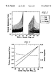
- FIG. 2 is a graph showing the variation of the thickness enhancement factor as a function of the radius of an annular ring for three different III-V compound semiconductor materials.
- FIG. 3 is a graph showing the variation in thickness enhancement factor and indium composition variation as a function of the width of the annular ring. Nominal thickness and In composition on a planar wafer are 1 and 0.18 respectively.
- FIG. 4 is a graph showing wavelength variation (Fabry-Perot cavity wavelength and modeled emission wavelength) as a function of annular ring width. The variations result from enhancement of thickness and In composition caused by varying ring mask width.
- FIG. 5 is a graph showing thickness enhancement at the center of the rings as a function of the width of the annular rings.
- FIG. 6 is a schematic diagram of a wavelength-selective RCPD array showing responsivity peaks at different wavelengths for elements with different cavity thicknesses.
- One embodiment of the present invention is a 2-dimensional VCSEL array that was built by applying the SAG technique to MOVPE.
- the variation of the mask geometry e.g., the mask area/shape or the open area/shape
- the variation of the mask geometry leads to a variation of the layer thickness and alloy compositions.
- the variation of the mask geometry can be in linear dimension or circumference (in the case of circular masks).
- Shown in FIG. 1 is a 4 ⁇ 4 array of the annular rings with the same inner opening-area diameter of 120 ⁇ m.
- the difference in the width of the rings (masked area) leads to a difference in the thickness of the material inside the ring.
- FIG. 2 shows the thickness profile in the open area of the substrate for the different patterns calculated for InAs, GaAs and In 0.18 Ga 0.82 As using trimethylgallium (TMG) and trimethylindium (TMI) as the metalorganic sources.
- TMG trimethylgallium
- TMI trimethylindium
- the growth pressure and growth temperature were 60 torr and 720° C., respectively, for this calculation.
- the thickness enhancement factor is normalized to the growth thickness on a featureless planar substrate. Since the source depletes almost exponentially away from the edge of the mask, the thickness varies over the whole radius of the feature. Use of the annular pattern helps to form a flatter profile in the open area.
- FIG. 2 shows the GaAs and InAs thickness are enhanced by very different amounts, being much steeper for InAs and GaAs, as a result of the difference in diffusion constants of the TMG and TMI.
- FIG. 3 shows the thickness enhancement factor and the In composition variation of InAsAs in the middle of the ring.
- the thickness variation was designed to be in a range of ⁇ 8% so that ⁇ 70 nm of variation of cavity wavelength can be achieved.
- the In composition also varies from 0.181 to 0.194. This can be extremely useful in defining different emission wavelengths for the gain of the quantum well active region.
- FIG. 4 shows the calculated cavity wavelength variation due to the thickness variation.
- the width of the mask was designed to achieve a total variation of the lasing wavelength of 40 nm.
- the stopband width of GaAs/Al 0.94 Ga 0.06 As is usually ⁇ 100 nm, so all the wavelengths are still covered within the single DBR structure.
- the gain wavelength doesn't change with the operating wavelength, the overlap of the gain with the cavity mode can vary significantly for the different elements of the array. As a result, the performance of the devices will be compromised, and they will only be able to run in a narrow temperature range.
- the In composition varies in the center of the doughnut, as shown in FIG. 3, in addition to the thickness.
- the variation in emission energy from the quantum wells with different In compositions and well thickness are calculated and plotted in FIG. 4 with the dotted line for the ring pattern.
- the emission wavelength moves in the same direction as the cavity wavelength modulated by the thickness variation, although they do not change at exactly the same rates.
- FIG. 5 shows the thickness in the middle of the ring for the growth of InGaAs/GaAs quantum wells with AlGaAs cladding layers for 980-nm VCSELs as a function of the mask width.
- the thick solid line represents the model calculation for the thickness enhancement, and the solid circles are measured thickness. The experimental results are in an excellent agreement with the calculation.
- the low-index material in the DBR is typically high Al composition AlGaAs or AlAs.
- AlGaAs or AlAs it is extremely difficult to achieve a perfect selectivity of AlAs on the dielectric mask. Therefore, a bottom DBR is grown first, the sample is then unloaded for patterning of the dielectric mask. This is followed by a SAG of the active region and the top DBR can then be grown on atop.
- a SAG of the active region we have demonstrated that the VCSEL performance from the selective area regrowth is almost identical to that from a single growth.
- the remaining steps for forming a VSCEL array are accomplished in a conventional manner, i.e. vertical etching to form the individual VCSEL elements, formation of electrodes, etc.
- the growth has to be extremely uniform.
- the wavelength accuracy can be further improved by in situ control using normal-incidence reflectance as the sensor (see W. G. Breiland, H. Q. Hou, H. C. Chui, and B. E. Hammons, “In situ pregrowth calibration using reflectance as a control strategy for MOCVD fabrication of device structures,” J. Cryst. Growth, vol. 174, pp. 564-568, 1997, incorporated by reference herein).
- two or more vertical optical resonant cavity structures can be formed using annular mask patterns with different inner diameters.
- the responsivity can be very high because of multiple paths through the active region.
- a schematic diagram of the detector array is shown in FIG. 6 .
- the tapered thickness is produced here by a linear mask that is configured in a V shape with equal widths on the arms of the V. The thickest portion of the cavity forms at the narrow end of the V, and the cavity thickness decreases as the V opens up.
- this structure could be formed between parallel linear edges of two trapezoidal-shaped mask strips.
- the thickest portion of the optical cavity would be formed adjacent to the portions of the mask strips having the greatest width.
- a combination of these two masking techniques could also be employed.
- This densely packed detector array sensitive to only a narrow wavelength range for each element, can function as a combination of bulky spectral dispersive device and a detector array, will be very appealing for a compact sensing system application.
Abstract
Description
Claims (8)
Priority Applications (1)
| Application Number | Priority Date | Filing Date | Title |
|---|---|---|---|
| US09/191,070 US6258615B1 (en) | 1998-11-12 | 1998-11-12 | Method of varying a characteristic of an optical vertical cavity structure formed by metalorganic vapor phase epitaxy |
Applications Claiming Priority (1)
| Application Number | Priority Date | Filing Date | Title |
|---|---|---|---|
| US09/191,070 US6258615B1 (en) | 1998-11-12 | 1998-11-12 | Method of varying a characteristic of an optical vertical cavity structure formed by metalorganic vapor phase epitaxy |
Publications (1)
| Publication Number | Publication Date |
|---|---|
| US6258615B1 true US6258615B1 (en) | 2001-07-10 |
Family
ID=22704016
Family Applications (1)
| Application Number | Title | Priority Date | Filing Date |
|---|---|---|---|
| US09/191,070 Expired - Lifetime US6258615B1 (en) | 1998-11-12 | 1998-11-12 | Method of varying a characteristic of an optical vertical cavity structure formed by metalorganic vapor phase epitaxy |
Country Status (1)
| Country | Link |
|---|---|
| US (1) | US6258615B1 (en) |
Cited By (5)
| Publication number | Priority date | Publication date | Assignee | Title |
|---|---|---|---|---|
| US6879612B1 (en) * | 2001-01-23 | 2005-04-12 | Optical Communication Products, Inc. | Temperature insensitive VCSEL |
| US7254155B1 (en) * | 2002-07-18 | 2007-08-07 | Finisar Corporation | High power single mode vertical cavity surface emitting laser |
| WO2010105865A2 (en) | 2009-03-19 | 2010-09-23 | Osram Opto Semiconductors Gmbh | Optoelectronic semiconductor component |
| US20160352073A1 (en) * | 2015-05-28 | 2016-12-01 | Vixar | Vcsels and vcsel arrays designed for improved performance as illumination sources and sensors |
| US20180175587A1 (en) * | 2015-06-04 | 2018-06-21 | Hewlett Packard Enterprise Development Lp | Monolithic wdm vcsels with spatially varying gain peak and fabry perot wavelength |
Citations (2)
| Publication number | Priority date | Publication date | Assignee | Title |
|---|---|---|---|---|
| US5659640A (en) * | 1995-06-27 | 1997-08-19 | Lucent Technologies Inc. | Integrated waveguide having an internal optical grating |
| US5960024A (en) * | 1998-03-30 | 1999-09-28 | Bandwidth Unlimited, Inc. | Vertical optical cavities produced with selective area epitaxy |
-
1998
- 1998-11-12 US US09/191,070 patent/US6258615B1/en not_active Expired - Lifetime
Patent Citations (2)
| Publication number | Priority date | Publication date | Assignee | Title |
|---|---|---|---|---|
| US5659640A (en) * | 1995-06-27 | 1997-08-19 | Lucent Technologies Inc. | Integrated waveguide having an internal optical grating |
| US5960024A (en) * | 1998-03-30 | 1999-09-28 | Bandwidth Unlimited, Inc. | Vertical optical cavities produced with selective area epitaxy |
Cited By (13)
| Publication number | Priority date | Publication date | Assignee | Title |
|---|---|---|---|---|
| US6879612B1 (en) * | 2001-01-23 | 2005-04-12 | Optical Communication Products, Inc. | Temperature insensitive VCSEL |
| US7254155B1 (en) * | 2002-07-18 | 2007-08-07 | Finisar Corporation | High power single mode vertical cavity surface emitting laser |
| WO2010105865A2 (en) | 2009-03-19 | 2010-09-23 | Osram Opto Semiconductors Gmbh | Optoelectronic semiconductor component |
| DE102009013909A1 (en) * | 2009-03-19 | 2010-09-23 | Osram Opto Semiconductors Gmbh | Optoelectronic semiconductor device |
| WO2010105865A3 (en) * | 2009-03-19 | 2011-01-13 | Osram Opto Semiconductors Gmbh | Optoelectronic semiconductor component |
| CN102356522A (en) * | 2009-03-19 | 2012-02-15 | 奥斯兰姆奥普托半导体有限责任公司 | Optoelectronic semiconductor component |
| US20160352073A1 (en) * | 2015-05-28 | 2016-12-01 | Vixar | Vcsels and vcsel arrays designed for improved performance as illumination sources and sensors |
| US10135222B2 (en) | 2015-05-28 | 2018-11-20 | Vixar | VCSELs and VCSEL arrays designed for improved performance as illumination sources and sensors |
| US10177527B2 (en) * | 2015-05-28 | 2019-01-08 | Vixar Inc. | VCSELS and VCSEL arrays designed for improved performance as illumination sources and sensors |
| US10749312B2 (en) | 2015-05-28 | 2020-08-18 | Vixar, Inc. | VCSELs and VCSEL arrays designed for improved performance as illumination sources and sensors |
| US11641091B2 (en) | 2015-05-28 | 2023-05-02 | Vixar, Inc. | VCSELs and VCSEL arrays designed for improved performance as illumination sources and sensors |
| US20180175587A1 (en) * | 2015-06-04 | 2018-06-21 | Hewlett Packard Enterprise Development Lp | Monolithic wdm vcsels with spatially varying gain peak and fabry perot wavelength |
| US10868407B2 (en) * | 2015-06-04 | 2020-12-15 | Hewlett Packard Enterprise Development Lp | Monolithic WDM VCSELS with spatially varying gain peak and fabry perot wavelength |
Similar Documents
| Publication | Publication Date | Title |
|---|---|---|
| Chang-Hasnain et al. | Multiple wavelength tunable surface-emitting laser arrays | |
| US5960024A (en) | Vertical optical cavities produced with selective area epitaxy | |
| KR101148287B1 (en) | Vcsel having an air gap and protective coating | |
| KR101252469B1 (en) | Buried heterostructure device having integrated waveguide grating fabricated by single step mocvd | |
| JP3540042B2 (en) | Manufacturing method of semiconductor device | |
| EP1030420B1 (en) | A vertical cavity surface emitting laser array and a process for making same | |
| JP2015508243A (en) | Surface emitting multi-wavelength distributed feedback concentric ring laser | |
| US7858417B2 (en) | Dielectric VCSEL gain guide | |
| US6084900A (en) | Annular waveguide vertical cavity surface emitting laser array and method of fabrication | |
| US6174749B1 (en) | Fabrication of multiple-wavelength vertical-cavity opto-electronic device arrays | |
| US6258615B1 (en) | Method of varying a characteristic of an optical vertical cavity structure formed by metalorganic vapor phase epitaxy | |
| US6693934B2 (en) | Wavelength division multiplexed vertical cavity surface emitting laser array | |
| Cockerill et al. | Twelve-channel strained-layer InGaAs-GaAs-AlGaAs buried heterostructure quantum well laser array for WDM applications by selective-area MOCVD | |
| US6061485A (en) | Method for wavelength division multiplexing utilizing donut mode vertical cavity surface emitting lasers | |
| Luong et al. | Monolithic wavelength-graded VCSEL and resonance-enhanced photodetector arrays for parallel optical interconnects | |
| US6989312B2 (en) | Method for fabricating semiconductor optical device | |
| WO1997050109A2 (en) | Vertical-cavity surface-emitting laser array | |
| Saito et al. | Monolithic integration of multiple wavelength vertical‐cavity surface‐emitting lasers by mask molecular beam epitaxy | |
| KR100754156B1 (en) | Multiple wavelength vertical-cavity surface emitting laser and method for manufacturing thereof | |
| Shin et al. | Fabrication method for multiple wavelength vertical-cavity emitter arrays by SiN x layer thickness control | |
| Yang et al. | Monolithic oxide-confined multiple-wavelength vertical-cavity surface-emitting laser arrays with a 57-nm wavelength grading range using an oxidized upper Bragg mirror | |
| US11876350B2 (en) | Multi-wavelength VCSEL array and method of fabrication | |
| US20240136803A1 (en) | Multi-wavelength vcsel array and method of fabrication | |
| Zhou et al. | Oxide-confined monolithic, multiple-wavelength vertical-cavity surface-emitting laser arrays with a 40-nm wavelength span | |
| JPH06283802A (en) | Semiconductor laser device and fabrication thereof |
Legal Events
| Date | Code | Title | Description |
|---|---|---|---|
| AS | Assignment |
Owner name: SANDIA CORPORATION, NEW MEXICO Free format text: ASSIGNMENT OF ASSIGNORS INTEREST;ASSIGNORS:HOU, HONG Q.;COLTRIN, MICHAEL E.;CHOQUETTE, KENT D.;REEL/FRAME:009702/0736;SIGNING DATES FROM 19981119 TO 19981210 |
|
| STCF | Information on status: patent grant |
Free format text: PATENTED CASE |
|
| FPAY | Fee payment |
Year of fee payment: 4 |
|
| AS | Assignment |
Owner name: ENERGY, U.S. DEPARTMENT OF, DISTRICT OF COLUMBIA Free format text: CONFIRMATORY LICENSE;ASSIGNOR:SANDIA CORPORATION;REEL/FRAME:016038/0069 Effective date: 19990113 |
|
| AS | Assignment |
Owner name: ENERGY, U.S. DEPARTMENT OF ENERGY, DISTRICT OF COL Free format text: CONFIRMATORY LICENSE;ASSIGNOR:SANDIA CORPORATION;REEL/FRAME:016256/0587 Effective date: 19990113 |
|
| FPAY | Fee payment |
Year of fee payment: 8 |
|
| FPAY | Fee payment |
Year of fee payment: 12 |
|
| AS | Assignment |
Owner name: NATIONAL TECHNOLOGY & ENGINEERING SOLUTIONS OF SAN Free format text: CHANGE OF NAME;ASSIGNOR:SANDIA CORPORATION;REEL/FRAME:043293/0702 Effective date: 20170501 |