US6304988B1 - Scan testable circuit arrangement - Google Patents
Scan testable circuit arrangement Download PDFInfo
- Publication number
- US6304988B1 US6304988B1 US09/531,103 US53110300A US6304988B1 US 6304988 B1 US6304988 B1 US 6304988B1 US 53110300 A US53110300 A US 53110300A US 6304988 B1 US6304988 B1 US 6304988B1
- Authority
- US
- United States
- Prior art keywords
- bus
- scan
- coupled
- logic circuits
- ports
- Prior art date
- Legal status (The legal status is an assumption and is not a legal conclusion. Google has not performed a legal analysis and makes no representation as to the accuracy of the status listed.)
- Expired - Lifetime
Links
Images


Classifications
-
- G—PHYSICS
- G06—COMPUTING; CALCULATING OR COUNTING
- G06F—ELECTRIC DIGITAL DATA PROCESSING
- G06F11/00—Error detection; Error correction; Monitoring
- G06F11/22—Detection or location of defective computer hardware by testing during standby operation or during idle time, e.g. start-up testing
- G06F11/26—Functional testing
- G06F11/267—Reconfiguring circuits for testing, e.g. LSSD, partitioning
-
- Y—GENERAL TAGGING OF NEW TECHNOLOGICAL DEVELOPMENTS; GENERAL TAGGING OF CROSS-SECTIONAL TECHNOLOGIES SPANNING OVER SEVERAL SECTIONS OF THE IPC; TECHNICAL SUBJECTS COVERED BY FORMER USPC CROSS-REFERENCE ART COLLECTIONS [XRACs] AND DIGESTS
- Y10—TECHNICAL SUBJECTS COVERED BY FORMER USPC
- Y10S—TECHNICAL SUBJECTS COVERED BY FORMER USPC CROSS-REFERENCE ART COLLECTIONS [XRACs] AND DIGESTS
- Y10S370/00—Multiplex communications
- Y10S370/908—Local area network
- Y10S370/911—Bridge, e.g. brouter, bus extender
Definitions
- the present invention relates to circuit arrangements for functionally testing logic circuits, and more particularly to a circuit arrangement for utilizing a common bus for functional operations of the logic circuits and for scan testing the logic circuits.
- Testing a logic circuit is often performed by loading test data into the logic circuit and, in a controlled manner, advancing the logic circuit from state to state. Various test data is output from the logic circuit and examined to determine whether the logic circuit is functioning as expected. Special scan test input/output pins are often provided for the input and output of the test data. Both parallel and serial designs exist for scanning-in and scanning-out test data via the scan test input/output pins. Parallel designs decrease the time required to load test data and read test results at the expense of increased pin resources. Serial designs conserve pin resources, but require additional time to load test data and read test results as compared to parallel designs.
- Increasing levels of circuit integration create at least two problems for scan testing logic circuits.
- a second problem is that a greater number of functional blocks of logic circuits on a chip creates increased demand for input/output pins for circuit access during normal operation, thereby competing with input/output pins used exclusively for scan testing.
- Cost-effective and efficient solutions for scan testing are highly desirable for the aforementioned reasons.
- present designs often trade pin resources against test time in implementing a desired level of cost-effectiveness and efficiency.
- the present invention is generally directed to a circuit arrangement and method that provides for functional testing of logic circuits, where a common bus is used for both a test mode and for a normal operational mode.
- a scan testable circuit arrangement includes a bus; a plurality of logic circuits having scan test ports; input/output ports; a first plurality of switches, each having a first terminal coupled to a predetermined signal line of the bus and a second terminal coupled to a respective one of scan test ports of the logic circuits; a second plurality of switches, each having a first terminal coupled to a predetermined signal line of the bus and a second terminal coupled to a respective one of input/output ports of the logic circuits; and a plurality of command decoders coupled to the bus for receiving bus commands and coupled to the gates of the first and second plurality of switches, responsive to a first set of commands for coupling the scan test ports to the bus for a first operational mode, and responsive to a second set of commands for coupling the input/output ports to the bus for a second operational mode.
- the scan test ports of each of the logic circuits are switchably coupled to a predetermined set of lines of the bus, each set respectively dedicated to one of the logic circuits.
- the logic circuits are organized into a plurality of groups, each group including predetermined ones of the logic circuits and predetermined ones of the command decoders, the first set of bus commands including respective codes for specifying each of the groups and the command decoders responsive to the respective codes, whereby each group is individually selectable for scan testing.
- the plurality of scan test ports include scan enable ports and scan clock ports, scan-in data ports, and scan-out data ports, the scan enable ports of the logic circuits switchably coupled to a predetermined first line of the bus, the scan clock ports of the logic circuits switchably coupled to a predetermined second line of the bus, the scan-in data port of a predetermined first one of the logic circuits switchably coupled to a predetermined third line of the bus, the scan-out data port of the first one of the logic circuits switchably coupled to a predetermined fourth line of the bus, the scan-in data port of each of the others of the logic circuits switchably coupled to the scan-out data port of another of the logic circuits via one of the lines of the bus, and the scan-output port of a predetermined last one of the logic circuits switchably coupled a predetermined fifth line of the bus.
- a method for scan testing logic circuits. The method involves transitting via a first bus a first command code to logic circuits that are coupled to the first bus; coupling scan test ports of the logic circuits to the first bus in response to the first command code; decoupling input/output circuits of the logic circuits from the first bus in response to the first command; inputting predetermined test data to the logic circuits via the bus; outputting data resulting from a test via the first bus; transmitting via the first bus a second command code to the logic circuits; decoupling scan test ports of the logic circuits from the first bus in response to the second command; and coupling input/output circuits of the logic circuits to the first bus in response to the second command.
- FIG. 1 is a functional block diagram of an example computer system according to one embodiment of the invention.
- FIG. 2 is a flow chart of an example method for scan testing according to an embodiment of the present invention
- FIG. 3 is a functional block diagram of an example bridge arrangement according to an embodiment of the present invention.
- FIG. 4 is a functional block diagram of example circuitry for switchably coupling scan test ports of logic circuits to a bus, according to an embodiment of the present invention
- FIG. 5 is a functional block diagram of another example embodiment of circuitry for switchably coupling scan test ports of logic circuits to a bus;
- FIG. 6 shows the relationship between FIGS. 6A and 6B, which together form a functional block diagram of another example embodiment of circuitry for switchably coupling scan test ports of logic circuits to a bus.
- the present invention is believed to be applicable to a variety of systems and arrangements having logic circuit blocks coupled to a bus.
- the invention has been found to be particularly advantageous in application environments where a bridge is also coupled to the bus to provide input and output of data and control signals to and from the logic circuit blocks, both for normal operations and for scan testing. While the present invention is not so limited, an appreciation of various aspects of the invention is best gained through a discussion of application examples operating in such an environment.
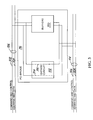
- FIG. 1 is a functional block diagram of a computer system 102 according to one embodiment of the invention.
- the computer system includes a host processor 104 coupled to a local bus 106 , where the local bus 106 has various peripherals attached thereto.
- the exemplary peripherals coupled to the local bus 106 include display 108 , system memory 110 , and circuit block 112 .
- the host processor 104 , local bus 106 display 108 , and system memory 110 are conventional components such as those typically included in a computer system using central processing units and/or chip sets available commercially, for example, from Intel, Texas Instruments, and Motorola.
- Circuit block 112 is an example circuit in which the present invention may be used. With respect to computer system 102 , circuit block 112 may implement any one of a variety of functions. Such functions include storage adapters, LAN adapters, graphics adapters, audio peripherals, video peripherals, and various other peripherals well-known to those skilled in the art. Circuit block 112 includes bus 114 and bridge 116 for coupling bus 114 to local bus 106 . The predetermined function or functions provided by circuit block 112 are provided by logic circuits 118 - 1 - 188 -n. The details of the function and/or functions provided by logic circuits 118 - 1 - 118 -n are beyond the scope of the present invention.
- Each of the logic circuits 118 - 1 - 118 -n is coupled to the bus 114 via a respective target circuit 120 - 1 - 120 -n.
- the respective target circuits 120 - 1 - 120 -n provide the interfaces between the logic circuits 118 - 1 - 118 -n and the bus 114 .
- bus 114 is a bus that is internal to an integrated circuit relative to targets 120 - 1 - 120 -n. In another embodiment, bus 114 may be external relative to target circuits 120 - 1 - 120 -n. In still another embodiment, bus 114 is a PCI bus (Peripheral Component Interconnect) and bridge 116 is a PCI bridge.
- PCI bus Peripheral Component Interconnect
- the present invention provides the capability to scan test logic circuits 118 - 1 - 118 -n via the bus 114 which is also used when the logic circuits 118 - 1 - 188 -n are operating according to their functional designs.
- bus 114 may be used for both normal runtime operations of computer system 102 and for functional testing of logic circuits 118 - 1 - 118 -n.
- no special pins are required for scan testing the logic circuits 118 - 1 - 118 -n.
- Scan control and data signals are input and output to and from the logic circuits 118 - 1 - 118 n via the bus 114 .
- FIG. 2 is a flow chart of an example method for scan testing consistent with the present invention. The method of FIG. 2 is described in the context of the computer system 102 of FIG. 1 . Processing begins at step 202 where a SCAN SETUP message is sent to the target circuits 120 - 1 - 120 -n via the bus 114 .
- the SCAN SETUP message causes scan test ports of the logic circuits 118 - 1 - 118 n to be coupled to associated signal lines of the bus 114 . Additionally, the normal clock signal port and the normal input/output/signal ports of the logic circuits 118 - 1 - 188 -n are disabled for scan testing.
- Step 204 illustrates coupling the scan ports of the logic circuits 118 - 1 - 118 -n to the bus 114
- step 206 illustrates disabling normal input/output ports of the logic circuits 118 - 1 - 118 n.
- a SCAN START message is sent to the bridge 116 as illustrated by step 208 .
- the SCAN START message causes lines of the local bus 106 to be directly coupled to associated lines of the bus 114 .
- Step 210 illustrates coupling lines of the local bus 106 to lines of the bus 114 by the bridge 116 .
- Steps 212 and 214 illustrate scanning in and scanning out test data to and from the logic circuits 118 - 1 - 118 -n for the purpose of testing the logic circuits.
- the particular data scanned in and testing sequence are dictated by the particular needs for testing logic circuits 118 - 1 - 118 n.
- Steps 216 - 222 illustrate the procedure for reestablishing the PCI connections.
- a SCAN STOP message is sent to the bridge 116 .
- the bridge 116 in response, disables the direct coupling of lines of the local bus 106 from the associated lines of the bus 114 as illustrated by step 218 .
- a SCAN DISABLE message is sent to the target circuits 120 - 1 - 120 n.
- the SCAN DISABLE message causes the target circuits 120 - 1 - 120 n to decouple scan test ports of the logic circuits 118 - 1 - 118 n from the associated lines in the bus, as illustrated by step 222 .
- the SCAN DISABLE message causes the target circuits 120 - 1 - 120 n to enable input/output ports for functional operation of the logic circuits 118 - 1 - 118 n, as illustrated at step 224 .
- FIG. 3 is a functional block diagram of a bridge 116 .
- bridge 116 is a PCI bridge, such as that described in copending patent application entitled, “ADDRESS/DATA QUEUING ARRANGEMENT AND METHOD FOR PROVIDING HIGH DATA THROUGH-PUT ACROSS BUS BRIDGE,” to Ronald Lange, having Ser. No., 08/721,252, filed Sep. 26, 1996, now U.S. Pat No. 5,941,970, assigned to the assignee of the present invention, and hereby incorporated by reference.
- the bridge 116 is coupled to command and control lines 302 and address and data lines 304 of local bus 106 and also coupled to command and control lines 306 and address and data lines 308 of bus 114 .
- bridge 116 directs command and control signals and address and data signals to buffers element 310 .
- Buffers 310 are used for interfacing the local bus 106 to bus 114 .
- the bridge In response to a SCAN START message sent to the bridge 116 , the bridge creates direct couplings between the lines of the local bus 106 and the bus 114 .
- the exemplary bridge 116 includes a bypass circuit 312 for creating the direct couplings between the local bus 106 and the bus 114 .
- Dashed line 314 in the bypass circuit 312 symbolizes that the bypass circuit 312 creates a direct coupling between the command and control lines 302 of the local bus 106 and the command and control lines 306 of the bus 114 in response to a SCAN START message.
- bypass circuit 312 creates a direct coupling between the address and data lines 304 of local bus 106 and the address and data lines 308 of bus 114 in response to the SCAN START message.
- the bypass circuit 312 disables the direct coupling of the command and control lines 306 of bus 114 from the command and control line 302 of local bus 106 as well as the address and data lines 308 of bus 114 from the address and data lines 304 of local bus 106 .
- Bypass circuit 312 may be implemented with circuitry that is similar to that described in the following FIGS.
- FIG. 4 is a functional block diagram of an example embodiment of circuitry for coupling scan test ports of logic circuits 118 - 1 - 118 - 8 to a bus 114 .
- Each of the logic circuits 118 - 1 through 118 - 8 is associated with four address and data lines of bus 114 for the purpose of scan testing.
- logic circuit 118 - 1 has scan test ports coupled to address and data lines AD[ 3 : 0 ], and logic circuit 118 - 8 as scan test ports coupled to address and data lines AD[ 31 : 28 ].
- the associated lines of the bus 114 are used for input of control and data signals and output of scan test data.
- the scan test ports of the logic circuits 118 - 1 through 118 - 8 are decoupled from the associated address and data lines of the bus 114 .
- Each of the targets 120 - 1 through 120 - 8 includes a respective command decoder 402 - 1 through 402 - 8 which is coupled to the command bus lines 404 of the bus 114 .
- Command decoder 402 - 1 switchably couples scan enable port 404 - 1 , scan clock port 406 - 1 , scan-in data port 408 - 1 , and scan-out data port 410 - 1 of logic circuit 118 - 1 to address and data lines AD[ 0 ], AD[ 1 ], AD[ 2 ], and AD[ 3 ], respectively.
- the command decoder 402 - 1 turns on switches 412 - 1 , 414 - 1 , 416 - 1 , and 418 - 1 , thereby coupling the scan test ports of logic circuit 118 - 1 to the associated lines of the bus 114 .
- Logic circuit 118 - 1 also includes input/output port 420 - 1 and clock port 422 - 1 , both of which are coupled to respective lines of the bus 114 . During scan testing, signals to and from the input/output port 420 - 1 and clock port 422 - 1 are disabled.
- command decoder 402 - 1 turns off switch elements 424 - 1 and 426 - 1 , thereby disabling inputs and outputs to and from the ports 420 - 1 and 422 - 1 of the logic circuit 118 - 1 .
- target circuit 120 - 8 operates in a manner which is similar to that of target circuit 120 - 1 .
- the scan test ports of logic circuit 118 - 8 are switchably coupled to different associated address and data lines of the bus 114 .
- address and data lines AD[ 28 ], AD[ 29 ], AD[ 30 ], and AD[ 31 ] are dedicated to the scan test ports of logic circuit 118 - 8 .
- predetermined ones of address and data lines AD[ 27 : 4 ] are respectively coupled to scan test ports of logic circuits 118 - 2 through 118 - 7 .
- logic circuits 118 - 2 through 118 - 7 are not shown in FIG. 4, but are represented by the ellipsis.
- the exemplary circuitry of FIG. 4 provides for up to eight logic circuits. However, those skilled in the art will recognize that additional logic circuits may be coupled to the bus 114 for the purpose of scan testing if additional address and data lines are available.
- FIG. 5 is a functional block diagram of another embodiment of circuitry for switchably coupling scan test ports of logic circuits to bus 114 .
- the embodiment of FIG. 5 entails grouping the logic circuits 118 - 1 through 118 -n and associated target circuits 120 - 1 through 120 -n such that different groups of circuits are selectable fbr scan testing using different scan test commands.
- target circuits 120 - 1 through 120 - 8 and the associated logic circuits 118 - 1 through 118 - 8 are included in group 1 , and scan testing via bus 114 is controlled with a SCAN- 1 type command input on command input lines 502 - 1 through 502 - 8 .
- a SCAN- 1 SETUP message is input on command lines 502 - 1 through 502 - 8 .
- Command decoder 504 - 1 detects SCAN- 1 type commands and switchably couples respective lines of the address and data bus to respective scan test ports 404 - 1 , 406 - 1 , 408 - 1 , and 410 - 1 of the logic circuit 118 - 1 .
- SCAN ENABLE port 404 - 1 is switchably coupled to address data line AD[ 0 ]
- SCAN CLOCK port 406 - 1 is switchably coupled to address and data line AD[ 1 ]
- SCAN-IN DATA port 408 - 1 is switchably coupled to address and data line AD[ 2 ]
- SCAN-OUT DATA port 410 - 1 is switchably coupled to address and data line AD[ 3 ].
- Command decoder 504 - 1 is different from command decoder 402 - 1 of FIG. 4 in that command decoder 504 - 1 is responsive to SCAN- 1 type commands which designate group 1 .
- Target circuits 120 - 2 - 120 - 8 include command decoders which are functionally similar to command decoder 504 - 1 .
- target circuits 120 - 25 - 120 - 32 include command decoders that are responsive to SCAN- 4 type commands.
- Target circuits of groups 2 and 3 (not shown) have command decoders that are responsive to SCAN- 2 and SCAN- 3 type commands, respectively.
- Each group of target circuits uses all of the address and data lines of the bus 114 for scan test purposes.
- logic circuit 118 - 1 uses address and data lines AD[ 3 : 0 ]
- logic circuit 118 - 2 (not shown) uses address and data lines AD[ 7 : 4 ]
- logic circuit 118 - 8 (not shown) of target circuit 120 - 8 uses address and data lines AD[ 31 : 28 ].
- Logic circuits 118 - 3 through 118 - 7 similarly use respective groups of four of address and data lines AD[ 27 : 8 ].
- Target circuits 120 - 9 - 120 - 16 of group 2 (not shown), target circuits 120 - 17 - 120 - 24 of group 3 (not shown), and target circuits 120 - 25 - 120 - 32 of group 4 are similarly coupled to address and data lines AD[ 31 : 0 ].
- FIG. 6 shows the relationship between FIGS. 6A and 6B, which together form a functional block diagram of another exemplary embodiment of circuitry for switchably coupling scan test ports of logic circuits to address and data lines of bus 114 .
- the SCAN ENABLE ports 404 - 1 , 404 - 2 , . . . , 404 - 28 , and 404 - 29 are all switchably coupled to address and data line AD[ 0 ].
- SCAN CLOCK ports 406 - 1 , 406 - 2 , . . . 406 - 28 , and 406 - 29 are all switchably coupled to address and data line AD[ 1 ].
- logic circuits 118 - 1 through 118 - 29 share the same SCAN ENABLE and SCAN CLOCK input signals.
- Address and data lines AD[ 31 : 2 ] of bus 114 form a scan chain for the logic circuits 118 - 1 through 118 - 29 .
- SCAN-IN DATA port 408 - 1 of logic circuit 118 - 1 is switchably coupled to address and data line AD[ 2 ]
- SCAN-OUT DATA port 410 - 1 is switchably coupled to address and data line AD[ 3 ], which is also coupled to SCAN-IN DATA port 408 - 2 of logic circuit 118 - 2 .
- SCAN-OUT DATA port 410 - 2 of logic circuit 118 - 2 being switchably coupled to address and data line AD[ 4 ], which is switchably coupled to SCAN-IN DATA port 408 - 3 of logic circuit 118 - 3 (not shown).
- SCAN-IN DATA port 408 -i of logic circuit 118 -i is switchably coupled to the same address and data line AD[j] as that which is switchably coupled to the SCAN-OUT DATA port 410 -(i ⁇ 1) of logic circuit 118 -(i ⁇ 1), except for a first one of the logic circuits.
- Command decoders 402 - 1 through 402 - 29 operate similarly to command decoders 402 - 1 through 402 - 8 of FIG. 4 .
Abstract
Description
Claims (12)
Priority Applications (1)
| Application Number | Priority Date | Filing Date | Title |
|---|---|---|---|
| US09/531,103 US6304988B1 (en) | 1997-10-27 | 2000-03-17 | Scan testable circuit arrangement |
Applications Claiming Priority (2)
| Application Number | Priority Date | Filing Date | Title |
|---|---|---|---|
| US08/958,530 US6041427A (en) | 1997-10-27 | 1997-10-27 | Scan testable circuit arrangement |
| US09/531,103 US6304988B1 (en) | 1997-10-27 | 2000-03-17 | Scan testable circuit arrangement |
Related Parent Applications (1)
| Application Number | Title | Priority Date | Filing Date |
|---|---|---|---|
| US08/958,530 Continuation US6041427A (en) | 1997-10-27 | 1997-10-27 | Scan testable circuit arrangement |
Publications (1)
| Publication Number | Publication Date |
|---|---|
| US6304988B1 true US6304988B1 (en) | 2001-10-16 |
Family
ID=25501026
Family Applications (2)
| Application Number | Title | Priority Date | Filing Date |
|---|---|---|---|
| US08/958,530 Expired - Lifetime US6041427A (en) | 1997-10-27 | 1997-10-27 | Scan testable circuit arrangement |
| US09/531,103 Expired - Lifetime US6304988B1 (en) | 1997-10-27 | 2000-03-17 | Scan testable circuit arrangement |
Family Applications Before (1)
| Application Number | Title | Priority Date | Filing Date |
|---|---|---|---|
| US08/958,530 Expired - Lifetime US6041427A (en) | 1997-10-27 | 1997-10-27 | Scan testable circuit arrangement |
Country Status (1)
| Country | Link |
|---|---|
| US (2) | US6041427A (en) |
Cited By (4)
| Publication number | Priority date | Publication date | Assignee | Title |
|---|---|---|---|---|
| US6665268B1 (en) * | 1999-08-31 | 2003-12-16 | Fujitsu Limited | Load testing apparatus, computer readable recording medium for recording load test program, fault diagnosis apparatus, and computer readable recording medium for recording fault diagnosis program |
| US6728822B1 (en) * | 1999-03-12 | 2004-04-27 | International Business Machines Corporation | Bus bridge circuit, information processing system and cardbus controller |
| US20050055615A1 (en) * | 2003-09-08 | 2005-03-10 | Agashe Anupama Anlruddha | At-speed ATPG testing and apparatus for SoC designs having multiple clock domain using a VLCT test platform |
| US20060036843A1 (en) * | 2001-10-30 | 2006-02-16 | Microsoft Corporation | Network interface sharing methods and apparatuses that support kernel mode data traffic and user mode data traffic |
Families Citing this family (3)
| Publication number | Priority date | Publication date | Assignee | Title |
|---|---|---|---|---|
| US6041427A (en) * | 1997-10-27 | 2000-03-21 | Vlsi Technology | Scan testable circuit arrangement |
| DE50015199D1 (en) * | 2000-01-26 | 2008-07-24 | Infineon Technologies Ag | Electrical circuit and method for testing a circuit component of the electrical circuit |
| US7127652B2 (en) * | 2003-06-03 | 2006-10-24 | Agilent Technologies, Inc. | X-tree test method and apparatus in a multiplexed digital system |
Citations (6)
| Publication number | Priority date | Publication date | Assignee | Title |
|---|---|---|---|---|
| US4357703A (en) * | 1980-10-09 | 1982-11-02 | Control Data Corporation | Test system for LSI circuits resident on LSI chips |
| US4625310A (en) * | 1984-04-23 | 1986-11-25 | Mercer M Ray | Universally testable logic elements and method for structural testing of logic circuits formed of such logic elements |
| US4926424A (en) * | 1987-06-11 | 1990-05-15 | Mitsubishi Denki Kabushiki Kaisha | Test auxiliary circuit for testing semiconductor device |
| US5161160A (en) * | 1989-02-07 | 1992-11-03 | Kabushiki Kaisha Toshiba | Circuit for testability |
| US5471481A (en) * | 1992-05-18 | 1995-11-28 | Sony Corporation | Testing method for electronic apparatus |
| US6041427A (en) * | 1997-10-27 | 2000-03-21 | Vlsi Technology | Scan testable circuit arrangement |
-
1997
- 1997-10-27 US US08/958,530 patent/US6041427A/en not_active Expired - Lifetime
-
2000
- 2000-03-17 US US09/531,103 patent/US6304988B1/en not_active Expired - Lifetime
Patent Citations (6)
| Publication number | Priority date | Publication date | Assignee | Title |
|---|---|---|---|---|
| US4357703A (en) * | 1980-10-09 | 1982-11-02 | Control Data Corporation | Test system for LSI circuits resident on LSI chips |
| US4625310A (en) * | 1984-04-23 | 1986-11-25 | Mercer M Ray | Universally testable logic elements and method for structural testing of logic circuits formed of such logic elements |
| US4926424A (en) * | 1987-06-11 | 1990-05-15 | Mitsubishi Denki Kabushiki Kaisha | Test auxiliary circuit for testing semiconductor device |
| US5161160A (en) * | 1989-02-07 | 1992-11-03 | Kabushiki Kaisha Toshiba | Circuit for testability |
| US5471481A (en) * | 1992-05-18 | 1995-11-28 | Sony Corporation | Testing method for electronic apparatus |
| US6041427A (en) * | 1997-10-27 | 2000-03-21 | Vlsi Technology | Scan testable circuit arrangement |
Cited By (21)
| Publication number | Priority date | Publication date | Assignee | Title |
|---|---|---|---|---|
| US6728822B1 (en) * | 1999-03-12 | 2004-04-27 | International Business Machines Corporation | Bus bridge circuit, information processing system and cardbus controller |
| US6665268B1 (en) * | 1999-08-31 | 2003-12-16 | Fujitsu Limited | Load testing apparatus, computer readable recording medium for recording load test program, fault diagnosis apparatus, and computer readable recording medium for recording fault diagnosis program |
| US20060129790A1 (en) * | 2001-10-30 | 2006-06-15 | Microsoft Corporation | Network interface sharing methods and apparatuses that support kernel mode data traffic and user mode data traffic |
| US7174449B2 (en) * | 2001-10-30 | 2007-02-06 | Microsoft Corporation | Network interface sharing methods and apparatuses that support kernel mode data traffic and user mode data traffic |
| US20060036842A1 (en) * | 2001-10-30 | 2006-02-16 | Microsoft Corporation | Network interface sharing methods and apparatuses that support kernel mode data traffic and user mode data traffic |
| US20060036839A1 (en) * | 2001-10-30 | 2006-02-16 | Microsoft Corporation | Network interface sharing methods and apparatuses that support kernel mode data traffic and user mode data traffic |
| US20060036841A1 (en) * | 2001-10-30 | 2006-02-16 | Microsoft Corporation | Networking interface sharing methods and apparatuses that support kernel mode data traffic and user mode data traffic |
| US20060036840A1 (en) * | 2001-10-30 | 2006-02-16 | Microsoft Corporation | Network interface sharing methods and apparatuses that support kernel mode data traffic and user mode data traffic |
| US20060053275A1 (en) * | 2001-10-30 | 2006-03-09 | Microsoft Corporation | Network interface sharing methods and apparatuses that support kernel mode data traffic and user mode data traffic |
| US20060059329A1 (en) * | 2001-10-30 | 2006-03-16 | Microsoft Corporation | Network interface sharing methods and apparatuses that support kernel mode data traffic and user mode data traffic |
| US7228409B2 (en) | 2001-10-30 | 2007-06-05 | Microsoft Corporation | Networking interface sharing methods and apparatuses that support kernel mode data traffic and user mode data traffic |
| US7228410B2 (en) | 2001-10-30 | 2007-06-05 | Microsoft Corporation | Network interface sharing methods and apparatuses that support kernel mode data traffic and user mode data traffic |
| US7167977B2 (en) | 2001-10-30 | 2007-01-23 | Microsoft Corporation | Network interface sharing methods and apparatuses that support kernel mode data traffic and user mode data traffic |
| US7167978B2 (en) * | 2001-10-30 | 2007-01-23 | Microsoft Corporation | Network interface sharing methods and apparatuses that support kernel mode data traffic and user mode data traffic |
| US7174448B2 (en) | 2001-10-30 | 2007-02-06 | Microsoft Corporation | Network interface sharing methods and apparatuses that support kernel mode data traffic and user mode data traffic |
| US20060036843A1 (en) * | 2001-10-30 | 2006-02-16 | Microsoft Corporation | Network interface sharing methods and apparatuses that support kernel mode data traffic and user mode data traffic |
| US7174450B2 (en) | 2001-10-30 | 2007-02-06 | Microsoft Corporation | Network interface sharing methods and apparatuses that support kernel mode data traffic and user mode data traffic |
| US7178018B2 (en) | 2001-10-30 | 2007-02-13 | Microsoft Corporation | Network interface sharing methods and apparatuses that support kernel mode data traffic and user mode data traffic |
| US7178017B2 (en) | 2001-10-30 | 2007-02-13 | Microsoft Corporation | Network interface sharing methods and apparatuses that support kernel mode data traffic and user mode data traffic |
| US7134061B2 (en) | 2003-09-08 | 2006-11-07 | Texas Instruments Incorporated | At-speed ATPG testing and apparatus for SoC designs having multiple clock domain using a VLCT test platform |
| US20050055615A1 (en) * | 2003-09-08 | 2005-03-10 | Agashe Anupama Anlruddha | At-speed ATPG testing and apparatus for SoC designs having multiple clock domain using a VLCT test platform |
Also Published As
| Publication number | Publication date |
|---|---|
| US6041427A (en) | 2000-03-21 |
Similar Documents
| Publication | Publication Date | Title |
|---|---|---|
| US7046035B2 (en) | Programmable driver for an I/O pin of an integrated circuit | |
| US6509758B2 (en) | IC with digital and analog circuits and mixed signal I/O pins | |
| US5581698A (en) | Semiconductor integrated circuit device with test mode for testing CPU using external Signal | |
| US5254940A (en) | Testable embedded microprocessor and method of testing same | |
| EP0254981B1 (en) | Diagnostic circuit | |
| JP3433404B2 (en) | Integrated circuit with test circuit and test method | |
| JPH0689990A (en) | Gate array | |
| AU2266600A (en) | Method and apparatus for adding and removing components without powering down computer system | |
| KR100299149B1 (en) | Microcontrollers with N-bit data bus widths with I / O pins of N or less and how | |
| JP2000502445A (en) | JTAG high impedance test mode | |
| US5287464A (en) | Semiconductor multi-device system with logic means for controlling the operational mode of a set of input/output data bus drivers | |
| US6304988B1 (en) | Scan testable circuit arrangement | |
| EP0398816A2 (en) | Testing method, testing circuit and semiconductor integrated circuit having testing circuit | |
| US6543018B1 (en) | System and method to facilitate flexible control of bus drivers during scan test operations | |
| KR100375252B1 (en) | Data processing system | |
| US20030074510A1 (en) | Method and apparatus for sharing signal pins on an interface between a system controller and peripheral integrated circuits | |
| JPH0342732A (en) | Semiconductor integrated circuit | |
| KR100188170B1 (en) | Scannable interface to non-scannable microprocessor | |
| EP0915566A2 (en) | Reset circuit for flipflop | |
| US5657328A (en) | Scan design with expanded access capability | |
| KR20040014335A (en) | Linking addressable shadow port and protocol for serial bus networks | |
| US6157051A (en) | Multiple function array based application specific integrated circuit | |
| US20040205283A1 (en) | Interface module | |
| US5872796A (en) | Method for interfacing boundary-scan circuitry with linearized impedance control type output drivers | |
| US6141717A (en) | Microcomputer having bus isolation means for selectively coupling an external bus to either a memory bus or a peripheral bus for testing of memory and peripheral circuits |
Legal Events
| Date | Code | Title | Description |
|---|---|---|---|
| STCF | Information on status: patent grant |
Free format text: PATENTED CASE |
|
| CC | Certificate of correction | ||
| REMI | Maintenance fee reminder mailed | ||
| FPAY | Fee payment |
Year of fee payment: 4 |
|
| SULP | Surcharge for late payment | ||
| AS | Assignment |
Owner name: NXP B.V., NETHERLANDS Free format text: ASSIGNMENT OF ASSIGNORS INTEREST;ASSIGNOR:PHILIPS SEMICONDUCTORS INC.;REEL/FRAME:018645/0779 Effective date: 20061130 Owner name: PHILIPS SEMICONDUCTORS VLSI INC., NEW YORK Free format text: CHANGE OF NAME;ASSIGNOR:VLSI TECHNOLOGY, INC.;REEL/FRAME:018635/0570 Effective date: 19990702 |
|
| AS | Assignment |
Owner name: PHILIPS SEMICONDUCTORS INC., NEW YORK Free format text: CHANGE OF NAME;ASSIGNOR:PHILIPS SEMICONDUCTORS VLSI INC.;REEL/FRAME:018668/0255 Effective date: 19991220 |
|
| AS | Assignment |
Owner name: MORGAN STANLEY SENIOR FUNDING, INC., ENGLAND Free format text: SECURITY AGREEMENT;ASSIGNOR:NXP B.V.;REEL/FRAME:018806/0201 Effective date: 20061201 |
|
| FPAY | Fee payment |
Year of fee payment: 8 |
|
| AS | Assignment |
Owner name: VLSI TECHNOLOGY, INC., CALIFORNIA Free format text: ASSIGNMENT OF ASSIGNORS INTEREST;ASSIGNOR:LEVY, PAUL S.;REEL/FRAME:028354/0377 Effective date: 19971023 |
|
| FPAY | Fee payment |
Year of fee payment: 12 |
|
| AS | Assignment |
Owner name: PARTNERS FOR CORPORATE RESEARCH INTERNATIONAL, CAY Free format text: ASSIGNMENT OF ASSIGNORS INTEREST;ASSIGNOR:NXP B. V.;REEL/FRAME:031334/0449 Effective date: 20120907 |
|
| AS | Assignment |
Owner name: FUTURE LINK SYSTEMS, CALIFORNIA Free format text: ASSIGNMENT OF ASSIGNORS INTEREST;ASSIGNOR:PARTNERS FOR CORPORATE RESEARCH INTERNATIONAL;REEL/FRAME:032399/0965 Effective date: 20130808 |
|
| AS | Assignment |
Owner name: NXP B.V., NETHERLANDS Free format text: RELEASE BY SECURED PARTY;ASSIGNOR:MORGAN STANLEY SENIOR FUNDING, INC;REEL/FRAME:050315/0443 Effective date: 20190903 |