US6310360B1 - Intersystem crossing agents for efficient utilization of excitons in organic light emitting devices - Google Patents
Intersystem crossing agents for efficient utilization of excitons in organic light emitting devices Download PDFInfo
- Publication number
- US6310360B1 US6310360B1 US09/358,731 US35873199A US6310360B1 US 6310360 B1 US6310360 B1 US 6310360B1 US 35873199 A US35873199 A US 35873199A US 6310360 B1 US6310360 B1 US 6310360B1
- Authority
- US
- United States
- Prior art keywords
- molecule
- emissive
- layer
- intersystem crossing
- emission
- Prior art date
- Legal status (The legal status is an assumption and is not a legal conclusion. Google has not performed a legal analysis and makes no representation as to the accuracy of the status listed.)
- Expired - Lifetime
Links
- 239000000463 material Substances 0.000 claims abstract description 70
- 238000000862 absorption spectrum Methods 0.000 claims abstract description 12
- 238000000295 emission spectrum Methods 0.000 claims abstract description 12
- 239000003795 chemical substances by application Substances 0.000 claims description 49
- ZNJRONVKWRHYBF-VOTSOKGWSA-N 4-(dicyanomethylene)-2-methyl-6-julolidyl-9-enyl-4h-pyran Chemical group O1C(C)=CC(=C(C#N)C#N)C=C1\C=C\C1=CC(CCCN2CCC3)=C2C3=C1 ZNJRONVKWRHYBF-VOTSOKGWSA-N 0.000 claims description 37
- 230000000903 blocking effect Effects 0.000 claims description 32
- 239000002019 doping agent Substances 0.000 claims description 20
- 238000004020 luminiscence type Methods 0.000 claims description 14
- 230000003595 spectral effect Effects 0.000 claims description 14
- OAICVXFJPJFONN-UHFFFAOYSA-N Phosphorus Chemical compound [P] OAICVXFJPJFONN-UHFFFAOYSA-N 0.000 claims description 11
- 229910052751 metal Inorganic materials 0.000 claims description 7
- 239000002184 metal Substances 0.000 claims description 7
- STTGYIUESPWXOW-UHFFFAOYSA-N 2,9-dimethyl-4,7-diphenyl-1,10-phenanthroline Chemical compound C=12C=CC3=C(C=4C=CC=CC=4)C=C(C)N=C3C2=NC(C)=CC=1C1=CC=CC=C1 STTGYIUESPWXOW-UHFFFAOYSA-N 0.000 claims description 6
- 150000002902 organometallic compounds Chemical group 0.000 claims description 3
- 230000000737 periodic effect Effects 0.000 claims description 2
- 230000005525 hole transport Effects 0.000 claims 2
- VQGHOUODWALEFC-UHFFFAOYSA-N 2-phenylpyridine Chemical group C1=CC=CC=C1C1=CC=CC=N1 VQGHOUODWALEFC-UHFFFAOYSA-N 0.000 claims 1
- 230000003287 optical effect Effects 0.000 abstract description 5
- 239000010410 layer Substances 0.000 description 136
- 238000012546 transfer Methods 0.000 description 81
- UEEXRMUCXBPYOV-UHFFFAOYSA-N iridium;2-phenylpyridine Chemical compound [Ir].C1=CC=CC=C1C1=CC=CC=N1.C1=CC=CC=C1C1=CC=CC=N1.C1=CC=CC=C1C1=CC=CC=N1 UEEXRMUCXBPYOV-UHFFFAOYSA-N 0.000 description 30
- TVIVIEFSHFOWTE-UHFFFAOYSA-K tri(quinolin-8-yloxy)alumane Chemical compound [Al+3].C1=CN=C2C([O-])=CC=CC2=C1.C1=CN=C2C([O-])=CC=CC2=C1.C1=CN=C2C([O-])=CC=CC2=C1 TVIVIEFSHFOWTE-UHFFFAOYSA-K 0.000 description 23
- 238000000034 method Methods 0.000 description 21
- 239000007850 fluorescent dye Substances 0.000 description 20
- 230000007246 mechanism Effects 0.000 description 20
- VFUDMQLBKNMONU-UHFFFAOYSA-N 9-[4-(4-carbazol-9-ylphenyl)phenyl]carbazole Chemical group C12=CC=CC=C2C2=CC=CC=C2N1C1=CC=C(C=2C=CC(=CC=2)N2C3=CC=CC=C3C3=CC=CC=C32)C=C1 VFUDMQLBKNMONU-UHFFFAOYSA-N 0.000 description 17
- 230000006798 recombination Effects 0.000 description 15
- 238000005215 recombination Methods 0.000 description 15
- 230000032258 transport Effects 0.000 description 15
- 239000000370 acceptor Substances 0.000 description 12
- 230000005281 excited state Effects 0.000 description 11
- 230000008569 process Effects 0.000 description 11
- 230000001052 transient effect Effects 0.000 description 9
- 230000005283 ground state Effects 0.000 description 8
- 238000004768 lowest unoccupied molecular orbital Methods 0.000 description 8
- 238000001228 spectrum Methods 0.000 description 8
- 239000000975 dye Substances 0.000 description 7
- 125000003118 aryl group Chemical group 0.000 description 6
- 239000002800 charge carrier Substances 0.000 description 6
- 230000008878 coupling Effects 0.000 description 6
- 238000010168 coupling process Methods 0.000 description 6
- 238000005859 coupling reaction Methods 0.000 description 6
- 238000009792 diffusion process Methods 0.000 description 6
- 230000005284 excitation Effects 0.000 description 6
- 230000004044 response Effects 0.000 description 6
- 150000001875 compounds Chemical class 0.000 description 5
- 230000006870 function Effects 0.000 description 5
- 239000012044 organic layer Substances 0.000 description 5
- 239000011368 organic material Substances 0.000 description 5
- 230000007704 transition Effects 0.000 description 5
- 0 *C.*C.C1=CC2=N(C=C1)[Ir]/C1=C/C=C/N=C\21.C1=CC2=N(C=C1)[Ir]/C1=C/C=C\C=C\21.C1=CC2=N(C=N1)[Ir]/C1=C/C=C/C=C\21 Chemical compound *C.*C.C1=CC2=N(C=C1)[Ir]/C1=C/C=C/N=C\21.C1=CC2=N(C=C1)[Ir]/C1=C/C=C\C=C\21.C1=CC2=N(C=N1)[Ir]/C1=C/C=C/C=C\21 0.000 description 4
- 125000000217 alkyl group Chemical group 0.000 description 4
- 238000013459 approach Methods 0.000 description 4
- 230000007423 decrease Effects 0.000 description 4
- 238000004770 highest occupied molecular orbital Methods 0.000 description 4
- 238000004519 manufacturing process Methods 0.000 description 4
- 239000011159 matrix material Substances 0.000 description 4
- IBHBKWKFFTZAHE-UHFFFAOYSA-N n-[4-[4-(n-naphthalen-1-ylanilino)phenyl]phenyl]-n-phenylnaphthalen-1-amine Chemical group C1=CC=CC=C1N(C=1C2=CC=CC=C2C=CC=1)C1=CC=C(C=2C=CC(=CC=2)N(C=2C=CC=CC=2)C=2C3=CC=CC=C3C=CC=2)C=C1 IBHBKWKFFTZAHE-UHFFFAOYSA-N 0.000 description 4
- 230000015572 biosynthetic process Effects 0.000 description 3
- -1 brominated polycyclic aromatic compounds Chemical class 0.000 description 3
- 230000000052 comparative effect Effects 0.000 description 3
- 238000005401 electroluminescence Methods 0.000 description 3
- 230000002708 enhancing effect Effects 0.000 description 3
- 230000001965 increasing effect Effects 0.000 description 3
- 229910052741 iridium Inorganic materials 0.000 description 3
- 239000003446 ligand Substances 0.000 description 3
- 125000002524 organometallic group Chemical group 0.000 description 3
- 150000002907 osmium Chemical class 0.000 description 3
- 230000010287 polarization Effects 0.000 description 3
- 229920006395 saturated elastomer Polymers 0.000 description 3
- 239000007787 solid Substances 0.000 description 3
- XXMUCWWTRNHTGM-UHFFFAOYSA-N 2,7-diphenylfluoren-1-one Chemical compound O=C1C2=CC3=CC(C=4C=CC=CC=4)=CC=C3C2=CC=C1C1=CC=CC=C1 XXMUCWWTRNHTGM-UHFFFAOYSA-N 0.000 description 2
- IJGRMHOSHXDMSA-UHFFFAOYSA-N Atomic nitrogen Chemical compound N#N IJGRMHOSHXDMSA-UHFFFAOYSA-N 0.000 description 2
- FSZJWSVKWRFXNF-UHFFFAOYSA-N C1=CC=C2C(=C1)[Ir]C1=C2/C=C\C=C/1 Chemical compound C1=CC=C2C(=C1)[Ir]C1=C2/C=C\C=C/1 FSZJWSVKWRFXNF-UHFFFAOYSA-N 0.000 description 2
- 230000004888 barrier function Effects 0.000 description 2
- 230000008859 change Effects 0.000 description 2
- 239000003086 colorant Substances 0.000 description 2
- 230000000694 effects Effects 0.000 description 2
- 238000002474 experimental method Methods 0.000 description 2
- 239000010408 film Substances 0.000 description 2
- 239000011521 glass Substances 0.000 description 2
- 229910001385 heavy metal Inorganic materials 0.000 description 2
- 230000006872 improvement Effects 0.000 description 2
- AMGQUBHHOARCQH-UHFFFAOYSA-N indium;oxotin Chemical compound [In].[Sn]=O AMGQUBHHOARCQH-UHFFFAOYSA-N 0.000 description 2
- 238000002347 injection Methods 0.000 description 2
- 239000007924 injection Substances 0.000 description 2
- 230000003993 interaction Effects 0.000 description 2
- GKOZUEZYRPOHIO-UHFFFAOYSA-N iridium atom Chemical compound [Ir] GKOZUEZYRPOHIO-UHFFFAOYSA-N 0.000 description 2
- 150000002739 metals Chemical class 0.000 description 2
- 229910052757 nitrogen Inorganic materials 0.000 description 2
- 150000002894 organic compounds Chemical class 0.000 description 2
- 229910052762 osmium Inorganic materials 0.000 description 2
- 238000010791 quenching Methods 0.000 description 2
- 230000001235 sensitizing effect Effects 0.000 description 2
- 239000000126 substance Substances 0.000 description 2
- 239000000758 substrate Substances 0.000 description 2
- 239000010409 thin film Substances 0.000 description 2
- 125000005259 triarylamine group Chemical group 0.000 description 2
- 238000001771 vacuum deposition Methods 0.000 description 2
- VFMUXPQZKOKPOF-UHFFFAOYSA-N 2,3,7,8,12,13,17,18-octaethyl-21,23-dihydroporphyrin platinum Chemical compound [Pt].CCc1c(CC)c2cc3[nH]c(cc4nc(cc5[nH]c(cc1n2)c(CC)c5CC)c(CC)c4CC)c(CC)c3CC VFMUXPQZKOKPOF-UHFFFAOYSA-N 0.000 description 1
- OGGKVJMNFFSDEV-UHFFFAOYSA-N 3-methyl-n-[4-[4-(n-(3-methylphenyl)anilino)phenyl]phenyl]-n-phenylaniline Chemical compound CC1=CC=CC(N(C=2C=CC=CC=2)C=2C=CC(=CC=2)C=2C=CC(=CC=2)N(C=2C=CC=CC=2)C=2C=C(C)C=CC=2)=C1 OGGKVJMNFFSDEV-UHFFFAOYSA-N 0.000 description 1
- VRKJTYJGZZQENC-UHFFFAOYSA-M C1=CC2=CC=CN3=C2C(=C1)O[Zn]3 Chemical compound C1=CC2=CC=CN3=C2C(=C1)O[Zn]3 VRKJTYJGZZQENC-UHFFFAOYSA-M 0.000 description 1
- ZIBMOMRUIPOUQK-UHFFFAOYSA-N C1=CC=N2[Ir]C3=C(/C=C\C=C/3)C2=C1 Chemical compound C1=CC=N2[Ir]C3=C(/C=C\C=C/3)C2=C1 ZIBMOMRUIPOUQK-UHFFFAOYSA-N 0.000 description 1
- XMWRBQBLMFGWIX-UHFFFAOYSA-N C60 fullerene Chemical class C12=C3C(C4=C56)=C7C8=C5C5=C9C%10=C6C6=C4C1=C1C4=C6C6=C%10C%10=C9C9=C%11C5=C8C5=C8C7=C3C3=C7C2=C1C1=C2C4=C6C4=C%10C6=C9C9=C%11C5=C5C8=C3C3=C7C1=C1C2=C4C6=C2C9=C5C3=C12 XMWRBQBLMFGWIX-UHFFFAOYSA-N 0.000 description 1
- VWWNOOKNRHZMRK-UHFFFAOYSA-N CC12#C(C=CC=C1)C(N(C1=CC=CC=C1)C1=CC=C(C3=CC=C(N(C4=CC=CC=C4)C4=CC=CC5#C4C=CC=C5)C=C3)C=C1)=CC=C2 Chemical compound CC12#C(C=CC=C1)C(N(C1=CC=CC=C1)C1=CC=C(C3=CC=C(N(C4=CC=CC=C4)C4=CC=CC5#C4C=CC=C5)C=C3)C=C1)=CC=C2 VWWNOOKNRHZMRK-UHFFFAOYSA-N 0.000 description 1
- MCTQNEBFZMBRSQ-GEEYTBSJSA-N Chrysoidine Chemical compound Cl.NC1=CC(N)=CC=C1\N=N\C1=CC=CC=C1 MCTQNEBFZMBRSQ-GEEYTBSJSA-N 0.000 description 1
- DIFSABHBPHFAIT-SMHSOALZSA-N [C-]#[N+]/C(C#N)=C1\C=C(C)OC(/C=C/C2=CC3=C4C(=C2)CCCN4CCC3)=C1 Chemical compound [C-]#[N+]/C(C#N)=C1\C=C(C)OC(/C=C/C2=CC3=C4C(=C2)CCCN4CCC3)=C1 DIFSABHBPHFAIT-SMHSOALZSA-N 0.000 description 1
- 238000010521 absorption reaction Methods 0.000 description 1
- 150000001251 acridines Chemical class 0.000 description 1
- FZEYVTFCMJSGMP-UHFFFAOYSA-N acridone Chemical class C1=CC=C2C(=O)C3=CC=CC=C3NC2=C1 FZEYVTFCMJSGMP-UHFFFAOYSA-N 0.000 description 1
- 230000004075 alteration Effects 0.000 description 1
- 150000004056 anthraquinones Chemical class 0.000 description 1
- 230000008901 benefit Effects 0.000 description 1
- WURBFLDFSFBTLW-UHFFFAOYSA-N benzil Chemical compound C=1C=CC=CC=1C(=O)C(=O)C1=CC=CC=C1 WURBFLDFSFBTLW-UHFFFAOYSA-N 0.000 description 1
- 150000004054 benzoquinones Chemical class 0.000 description 1
- 238000006243 chemical reaction Methods 0.000 description 1
- 230000002860 competitive effect Effects 0.000 description 1
- 230000000295 complement effect Effects 0.000 description 1
- 238000010276 construction Methods 0.000 description 1
- 150000004696 coordination complex Chemical class 0.000 description 1
- 230000003111 delayed effect Effects 0.000 description 1
- 230000001419 dependent effect Effects 0.000 description 1
- 238000013461 design Methods 0.000 description 1
- 238000011161 development Methods 0.000 description 1
- 230000018109 developmental process Effects 0.000 description 1
- 150000004985 diamines Chemical class 0.000 description 1
- 238000005516 engineering process Methods 0.000 description 1
- 238000002189 fluorescence spectrum Methods 0.000 description 1
- 229910003472 fullerene Inorganic materials 0.000 description 1
- 229910052737 gold Inorganic materials 0.000 description 1
- 238000005286 illumination Methods 0.000 description 1
- 150000002503 iridium Chemical class 0.000 description 1
- 229930192419 itoside Natural products 0.000 description 1
- CUONGYYJJVDODC-UHFFFAOYSA-N malononitrile Chemical compound N#CCC#N CUONGYYJJVDODC-UHFFFAOYSA-N 0.000 description 1
- 150000002736 metal compounds Chemical class 0.000 description 1
- 239000000203 mixture Substances 0.000 description 1
- 238000004776 molecular orbital Methods 0.000 description 1
- 238000005457 optimization Methods 0.000 description 1
- 230000005693 optoelectronics Effects 0.000 description 1
- SYQBFIAQOQZEGI-UHFFFAOYSA-N osmium atom Chemical compound [Os] SYQBFIAQOQZEGI-UHFFFAOYSA-N 0.000 description 1
- 238000000059 patterning Methods 0.000 description 1
- 150000002988 phenazines Chemical class 0.000 description 1
- 238000009832 plasma treatment Methods 0.000 description 1
- 229910052697 platinum Inorganic materials 0.000 description 1
- BASFCYQUMIYNBI-UHFFFAOYSA-N platinum Substances [Pt] BASFCYQUMIYNBI-UHFFFAOYSA-N 0.000 description 1
- 229920003227 poly(N-vinyl carbazole) Polymers 0.000 description 1
- 238000007639 printing Methods 0.000 description 1
- 150000003216 pyrazines Chemical class 0.000 description 1
- 230000000171 quenching effect Effects 0.000 description 1
- ZUQDDQFXSNXEOD-UHFFFAOYSA-N quinoxalin-5-ol Chemical compound C1=CN=C2C(O)=CC=CC2=N1 ZUQDDQFXSNXEOD-UHFFFAOYSA-N 0.000 description 1
- 150000003252 quinoxalines Chemical class 0.000 description 1
- 239000004065 semiconductor Substances 0.000 description 1
- 239000000243 solution Substances 0.000 description 1
- 238000007614 solvation Methods 0.000 description 1
- 125000006850 spacer group Chemical group 0.000 description 1
- 238000002207 thermal evaporation Methods 0.000 description 1
- 150000005029 thianthrenes Chemical class 0.000 description 1
- 229930192474 thiophene Natural products 0.000 description 1
- 150000003577 thiophenes Chemical class 0.000 description 1
- 150000003852 triazoles Chemical class 0.000 description 1
- ODHXBMXNKOYIBV-UHFFFAOYSA-N triphenylamine Chemical compound C1=CC=CC=C1N(C=1C=CC=CC=1)C1=CC=CC=C1 ODHXBMXNKOYIBV-UHFFFAOYSA-N 0.000 description 1
- 229910052721 tungsten Inorganic materials 0.000 description 1
- 125000000391 vinyl group Chemical group [H]C([*])=C([H])[H] 0.000 description 1
- 238000001429 visible spectrum Methods 0.000 description 1
- 230000005428 wave function Effects 0.000 description 1
Images


Classifications
-
- H—ELECTRICITY
- H10—SEMICONDUCTOR DEVICES; ELECTRIC SOLID-STATE DEVICES NOT OTHERWISE PROVIDED FOR
- H10K—ORGANIC ELECTRIC SOLID-STATE DEVICES
- H10K50/00—Organic light-emitting devices
- H10K50/10—OLEDs or polymer light-emitting diodes [PLED]
- H10K50/18—Carrier blocking layers
-
- H—ELECTRICITY
- H05—ELECTRIC TECHNIQUES NOT OTHERWISE PROVIDED FOR
- H05B—ELECTRIC HEATING; ELECTRIC LIGHT SOURCES NOT OTHERWISE PROVIDED FOR; CIRCUIT ARRANGEMENTS FOR ELECTRIC LIGHT SOURCES, IN GENERAL
- H05B33/00—Electroluminescent light sources
- H05B33/12—Light sources with substantially two-dimensional radiating surfaces
- H05B33/14—Light sources with substantially two-dimensional radiating surfaces characterised by the chemical or physical composition or the arrangement of the electroluminescent material, or by the simultaneous addition of the electroluminescent material in or onto the light source
-
- H—ELECTRICITY
- H10—SEMICONDUCTOR DEVICES; ELECTRIC SOLID-STATE DEVICES NOT OTHERWISE PROVIDED FOR
- H10K—ORGANIC ELECTRIC SOLID-STATE DEVICES
- H10K50/00—Organic light-emitting devices
- H10K50/10—OLEDs or polymer light-emitting diodes [PLED]
- H10K50/11—OLEDs or polymer light-emitting diodes [PLED] characterised by the electroluminescent [EL] layers
- H10K50/12—OLEDs or polymer light-emitting diodes [PLED] characterised by the electroluminescent [EL] layers comprising dopants
- H10K50/121—OLEDs or polymer light-emitting diodes [PLED] characterised by the electroluminescent [EL] layers comprising dopants for assisting energy transfer, e.g. sensitization
-
- H—ELECTRICITY
- H10—SEMICONDUCTOR DEVICES; ELECTRIC SOLID-STATE DEVICES NOT OTHERWISE PROVIDED FOR
- H10K—ORGANIC ELECTRIC SOLID-STATE DEVICES
- H10K85/00—Organic materials used in the body or electrodes of devices covered by this subclass
- H10K85/30—Coordination compounds
- H10K85/341—Transition metal complexes, e.g. Ru(II)polypyridine complexes
- H10K85/342—Transition metal complexes, e.g. Ru(II)polypyridine complexes comprising iridium
-
- H—ELECTRICITY
- H10—SEMICONDUCTOR DEVICES; ELECTRIC SOLID-STATE DEVICES NOT OTHERWISE PROVIDED FOR
- H10K—ORGANIC ELECTRIC SOLID-STATE DEVICES
- H10K2101/00—Properties of the organic materials covered by group H10K85/00
- H10K2101/10—Triplet emission
-
- H—ELECTRICITY
- H10—SEMICONDUCTOR DEVICES; ELECTRIC SOLID-STATE DEVICES NOT OTHERWISE PROVIDED FOR
- H10K—ORGANIC ELECTRIC SOLID-STATE DEVICES
- H10K2102/00—Constructional details relating to the organic devices covered by this subclass
- H10K2102/10—Transparent electrodes, e.g. using graphene
- H10K2102/101—Transparent electrodes, e.g. using graphene comprising transparent conductive oxides [TCO]
- H10K2102/103—Transparent electrodes, e.g. using graphene comprising transparent conductive oxides [TCO] comprising indium oxides, e.g. ITO
-
- H—ELECTRICITY
- H10—SEMICONDUCTOR DEVICES; ELECTRIC SOLID-STATE DEVICES NOT OTHERWISE PROVIDED FOR
- H10K—ORGANIC ELECTRIC SOLID-STATE DEVICES
- H10K85/00—Organic materials used in the body or electrodes of devices covered by this subclass
- H10K85/30—Coordination compounds
- H10K85/321—Metal complexes comprising a group IIIA element, e.g. Tris (8-hydroxyquinoline) gallium [Gaq3]
- H10K85/324—Metal complexes comprising a group IIIA element, e.g. Tris (8-hydroxyquinoline) gallium [Gaq3] comprising aluminium, e.g. Alq3
-
- H—ELECTRICITY
- H10—SEMICONDUCTOR DEVICES; ELECTRIC SOLID-STATE DEVICES NOT OTHERWISE PROVIDED FOR
- H10K—ORGANIC ELECTRIC SOLID-STATE DEVICES
- H10K85/00—Organic materials used in the body or electrodes of devices covered by this subclass
- H10K85/30—Coordination compounds
- H10K85/341—Transition metal complexes, e.g. Ru(II)polypyridine complexes
- H10K85/348—Transition metal complexes, e.g. Ru(II)polypyridine complexes comprising osmium
-
- H—ELECTRICITY
- H10—SEMICONDUCTOR DEVICES; ELECTRIC SOLID-STATE DEVICES NOT OTHERWISE PROVIDED FOR
- H10K—ORGANIC ELECTRIC SOLID-STATE DEVICES
- H10K85/00—Organic materials used in the body or electrodes of devices covered by this subclass
- H10K85/60—Organic compounds having low molecular weight
- H10K85/631—Amine compounds having at least two aryl rest on at least one amine-nitrogen atom, e.g. triphenylamine
-
- H—ELECTRICITY
- H10—SEMICONDUCTOR DEVICES; ELECTRIC SOLID-STATE DEVICES NOT OTHERWISE PROVIDED FOR
- H10K—ORGANIC ELECTRIC SOLID-STATE DEVICES
- H10K85/00—Organic materials used in the body or electrodes of devices covered by this subclass
- H10K85/60—Organic compounds having low molecular weight
- H10K85/649—Aromatic compounds comprising a hetero atom
Definitions
- the present invention is directed to organic light emitting devices (OLEDs) comprised of emissive layers that contain an organic compound functioning as an emitter and a separate intersystem crossing (“ISC”) entity which operates to enhance the efficiency of the emission.
- OLEDs organic light emitting devices
- ISC intersystem crossing
- OLEDs Organic light emitting devices
- one of the layers is comprised of an organic material that can be made to electroluminesce by applying a voltage across the device, C. W. Tang et al., Appl. Phys. Lett. 1987, 51, 913.
- Certain OLEDs have been shown to have sufficient brightness, range of color and operating lifetimes for use as a practical alternative technology to LCD-based full color flat-panel displays (S. R. Forrest, P. E. Burrows and M. E. Thompson, Laser Focus World, Feb. 1995).
- a transparent OLED which represents a significant step toward realizing high resolution, independently addressable stacked R-G-B pixels, was reported in International Patent Application No. PCT/US97/02681 in which the TOLED had greater than 71% transparency when turned off and emitted light from both top and bottom device surfaces with high efficiency (approaching 1% quantum efficiency) when the device was turned on.
- the TOLED used transparent indium tin oxide (ITO) as the hole-injecting electrode and a Mg—Ag-ITO electrode layer for electron-injection.
- ITO transparent indium tin oxide
- Mg—Ag-ITO electrode layer for electron-injection.
- a device was disclosed in which the ITO side of the Mg—Ag-ITO layer was used as a hole-injecting contact for a second, different color-emitting OLED stacked on top of the TOLED.
- Each layer in the stacked OLED was independently addressable and emitted its own characteristic color. This colored emission could be transmitted through the adjacently stacked, transparent, independently addressable, organic layer or layers, the transparent contacts and the glass substrate, thus allowing the device to emit any color that could be produced by varying the relative output of the red and blue color-emitting layers.
- PCT/US95/15790 application disclosed an integrated SOLED for which both intensity and color could be independently varied and controlled with external power supplies in a color tunable display device.
- the PCT/US95/15790 application thus, illustrates a principle for achieving integrated, full color pixels that provide high image resolution, which is made possible by the compact pixel size.
- relatively low cost fabrication techniques as compared with prior art methods, may be utilized for making such devices.
- Luminescence from a symmetry-disallowed process is known as phosphorescence. Characteristically, phosphorescence may persist for up to several seconds afier excitation due to the low probability of the transition. In contrast, fluorescence originates in the rapid decay of a singlet exciton. Since this process occurs between states of like symmetry, it may be very efficient.
- This invention pertains to the use of intersystem crossing agents to enhance emission efficiency in organic light emitting devices.
- An intersystem crossing agent, or molecule is one which can undergo intersystem crossing, which involves the transfer of population between states of different spin multiplicity. Lists of known intersystem crossing agents, or molecules, are given in A. Gilbert and J. Baggott, Essentials of Molecular Photochemistry, Blackwells Scientific, 1991.
- the ISC agent traps the energy of excitons and transfers the energy to the fluorescent emitter by a Forster energy transfer.
- the energy transfer process desired is:
- D and A represent a donor molecule and a fluorescent acceptor, respectively.
- the superscripts 3 and 1 denote the triplet and singlet states, respectively, and the asterisk indicates the excited state.
- a second embodiment of the present invention we focus on a way to use an intersystem crossing agent to increase efficiency in a system with a phosphorescent emitter.
- the ISC agent is responsible for converting all of the excitons from a host material into their triplet states and then transferring that excited state to the phosphorescent emitter. This would include the case wherein the ISC agent only traps singlet excitons on the host and host triplet excitons are transferred directly to the phosphorescent emitter (rather than going through the ISC agent.)
- a phosphorescent emitter is combined with an intersystem crossing agent such that the following can occur:
- D represents the donor (host)
- X represents the intersystem crossing agent
- A represents the acceptor (emissive molecule).
- Superscript 1 denotes singlet spin multiplicity
- superscript 3 denotes triplet spin multiplicity
- the asterisk denotes an excited state.
- the intersystem crossing agent acts to convert singlet excitons to triplet excitons, thereby keeping singlets from reaching the emissive region and thus enhancing optical purity (the “filter” aspect: singlets are removed and thus no singlets emit) and increasing efficiency (the “conversion” aspect: singlets are converting to triplets, which do emit).
- dipoles on the donor and acceptor molecules couple and energy may be transferred. Dipoles are generated from allowed transitions in both donor and acceptor molecules. This typically restricts the Förster mechanism to transfers between singlet states.
- the transition on the donor ( 3 D* ⁇ 1 D) is allowed, i.e. the donor is a phosphorescent molecule.
- the probability of this transition is low because of symmetry differences between the excited triplet and ground state singlet.
- the phosphor can emit light due to some perturbation of the state such as due to spin-orbit coupling introduced by a heavy metal atom, it may participate as the donor in Förster transfer.
- the efficiency of the process is deternined by the luminescent efficiency of the phosphor (F Wilkinson, in Advances in Photochemistry (eds. W. A. Noyes, G. Hammond, and J. N. Pitts, pp. 241-268, John Wiley & Sons, New York, 1964), i.e. if a radiative transition is more probable than a non-radiative decay, then energy transfer will be efficient.
- Such triplet-singlet transfers were predicted by Förster (T.
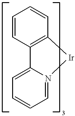
- Example 1 of this application we use the green phosphor fac tris(2-phenylpyridine) iridium (Ir(ppy) 3 ; M. A. Baldo, et al., Appl. Phys. Lett., 1999, 75, 4-6) and the red fluorescent dye [2-methyl-6-[2-(2,3,6,7-tetrahydro-1H,5H-benzo[ij]quinolizin-9-yl)ethenyl]-4H-pyran-ylidene] propane-dinitrile] (“DCM2”; C. W. Tang, S. A.
- X represents the sensitizer molecule and h ⁇ is the photon energy.
- FIG. 1 The multiple state energy transfer required in the phosphorescent-sensitized system is schematically described in FIG. 1 .
- Dexter transfers are indicated by dotted arrows, and Forster transfers by solid arrows. Transfers resulting in a loss in efficiency are marked with a cross.
- direct electron-hole recombination is possible on the phosphorescent and fluorescent dopants as well as the host.
- Triplet exciton formation after charge recombination on the fluorescent dye is another potential loss mechanism.
- Example 1 The details, given in Example 1 below, showed the improvement in efficiency of fluorescent yield brought about by the use of the phosphorescent sensitizer. In the following sections, we give additional background.
- OLEDs are comprised of at least two thin organic layers separating the anode and cathode of the device.
- the material of one of these layers is specifically chosen based on the material's ability to transport holes, a “hole transporting layer” (HTL), and the material of the other layer is specifically selected according to its ability to transport electrons, an “electron transporting layer” (ETL).
- HTL hole transporting layer
- ETL electron transporting layer
- the device can be viewed as a diode with a forward bias when the potential applied to the anode is higher than the potential applied to the cathode.
- the anode injects holes (positive charge carriers) into the hole transporting layer, while the cathode injects electrons into the electron transporting layer.
- the portion of the luminescent medium adjacent to the anode thus forms a hole injecting and transporting zone while the portion of the luminescent medium adjacent to the cathode forms an electron injecting and transporting zone.
- the injected holes and electrons each migrate toward the oppositely charged electrode. When an electron and hole localize on the same molecule, a Frenkel exciton is formed.
- the electroluminescent layer comprises a luminescence zone receiving mobile charge carriers (electrons and holes) from each electrode.
- triplet diffusion lengths are typically long (e.g., >1400 ⁇ ) compared with typical singlet diffusion lengths of about 200 ⁇ .
- an advantage of phosphorescence is that all excitons (formed by the recombination of holes and electrons in an EL), which are (in part) triplet-based in phosphorescent devices, may participate in energy transfer and luminescence in certain electroluminescent materials. In contrast, only a small percentage of excitons in fluorescent devices, which are singlet-based, result in fluorescent luminescence.
- An alternative is to use phosphorescence processes to improve the efficiency of fluorescence processes. Fluorescence is in principle 75% less efficient due the three times higher number of symmetric excited states.
- a phosphorescent sensitizer molecule to excite a fluorescent material in a red-emitting OLED.
- the mechanism for energetic coupling between molecular species is a long-range, non-radiative energy transfer from the phosphor to the fluorescent dye.
- the internal efficiency of fluorescence can be as high as 100%, a result previously only possible with phosphorescence. As shown in Example 1, we employ it to nearly quadruple the efficiency of a fluorescent OLED.
- one typically has at least one electron transporting layer and at least one hole transporting layer one has layers of different materials, forming a heterostructure.
- the materials that produce the electroluminescent emission may be the same materials that function either as the electron transporting layer or as the hole transporting layer.
- Such devices in which the electron transporting layer or the hole transporting layer also functions as the emissive layer are referred to as having a single heterostructure.
- the electroluminescent material may be present in a separate emissive layer between the hole transporting layer and the electron transporting layer in what is referred to as a double heterostructure.
- the separate emissive layer may contain the emissive molecule doped into a host or the emissive layer may consist essentially of the emissive molecule.
- the emissive material may be present in relatively low concentrations as a dopant in the charge carrier layer.
- the predominant material in the charge carrier layer may be referred to as a host compound or as a receiving compound.
- Materials that are present as host and dopant are selected so as to have a high level of energy transfer from the host to the dopant material. In addition, these materials need to be capable of producing acceptable electrical properties for the OLED.
- host and dopant materials are preferably capable of being incorporated into the OLED using materials that can be readily incorporated into the OLED by using convenient fabrication techniques, in particular, by using vacuum-deposition techniques.
- the exciton blocking layer used in the devices of the present invention substantially blocks the diffusion of excitons, thus substantially keeping the excitons within the emission layer to enhance device efficiency.
- the material of blocking layer of the present invention is characterized by an energy difference (“band gap”) between its lowest unoccupied molecular orbital (LUMO) and its highest occupied molecular orbital (HOMO) In accordance with the present invention, this band gap substantially prevents the diffusion of excitons through the blocking layer, yet has only a minimal effect on the turn-on voltage of a completed electroluminescent device.
- the band gap is thus preferably greater than the energy level of excitons produced in an emission layer, such that such excitons are not able to exist in the blocking layer.
- the band gap of the blocking layer is at least as great as the difference in energy between the triplet state and the ground state of the host.
- the difference in energy between the LUMO and HOMO of the blocking layer is greater than the difference in energy between the triplet and ground state singlet of the host material.
- Triplets in the host material are not quenched by the blocking layer.
- the ionization potential (IP) of the blocking layer is greater than the ionization potential of the host. (Meaning that holes are held in the host.)
- the energy level of the LUMO of the blocking layer and the energy level of the LUMO of the host are sufficiently close in energy such that there is less than 50% change in the overall conductivity of the device.
- the blocking layer is as thin as possible subject to having a thickness of the layer that is sufficient to effectively block the transport of excitons from the emissive layer into the adjacent layer.
- the ionization potential of the blocking layer should be greater than that of the HTL, while the electron affinity of the blocking layer should be approximately equal to that of the ETL to allow for facile transport of electrons.
- the difference in energy between the LUMO and HOMO of the blocking layer is greater than the difference in energy between the triplet and ground state singlet of the host material.
- Triplets in the host material are not quenched by the blocking layer.
- the energy of the LUMO of the blocking layer is greater than the energy of the LUMO of the (electron-transporting) host. (Meaning that electrons are held in the host.)
- the ionization potential of the blocking layer and the ionization potential of the host are such that holes are readily injected from the blocker into the host and there is less than a 50% change in the overall conductivity of the device.
- the blocking layer is as thin as possible subject to having a thickness of the layer that is sufficient to effectively block the transport of excitons from the emissive layer into the adjacent layer.
- OLEDs As to colors, it is desirable for OLEDs to be fabricated using materials that provide electroluminescent emission in a relatively narrow band centered near selected spectral regions, which correspond to one of the three primary colors, red, green and blue so that they may be used as a colored layer in an OLED or SOLED. It is also desirable that such compounds be capable of being readily deposited as a thin layer using vacuum deposition techniques so that they may be readily incorporated into an OLED that is prepared entirely from vacuum-deposited organic materials.
- the present invention is directed to organic light emitting devices comprising an emissive layer wherein the emissive layer comprises an emissive molecule, with a host material (wherein the emissive molecule present as a dopant in said host material) which molecule is adapted to luminesce when a voltage is applied across a heterostructure, wherein the emissive molecule is selected from the group of phosphorescent or fluorescent organic molecules and wherein the device comprises a molecule which can function as an intersystem crossing agent (“ISC molecule”) which improves the efficiency of the phosphorescence or fluorescence relative to the situation where the ISC molecule is absent.
- ISC molecule intersystem crossing agent
- a fluorescent emitter is combined with a phosphorescent sensitizer, which operates as an intersystem crossing agent.
- the phosphorescent sensitizer may be selected from materials wherein the radiative recombination rate is much greater than the non-radiative rate of recombination.
- the phosphorescent sensitizer may be selected from the group of cyclometallated organometallic compounds.
- the metal thereof may be selected from metals of the third row of the periodic table (especially W, Pt, Au, Ir, Os) and any other metals or metal compounds that have strong spin orbit coupling.
- the phosphorescent sensitizer may be further selected from the group of phosphorescent organometallic iridium or osmium complexes and may be still further selected from the group of phosphorescent cyclometallated iridium or osmium complexes.
- a specific example of the sensitizer molecule is fac tris(2-phenylpyridine) iridium, denoted (Ir(ppy) 3 ) of formula
- DCM2 of formula
- a phosphorescent emitter is combined with an intersystem crossing agent such that the following can occur:
- D represents the donor (host)
- X represents the intersystem crossing agent
- A represents the acceptor (emissive molecule).
- Superscript 1 denotes singlet spin multiplicity
- superscript 3 denotes triplet spin multiplicity
- the asterisk denotes an excited state.
- a thin layer of an ISC agent is placed in the device; it may be between the HTL and ETL.
- the ISC agent is selected such that the optical absorption spectrum of the ISC agent overlaps strongly with the emission line of the material found at the site of recombination.
- the general arrangement of the heterostructure of the devices is such that the layers are ordered hole transporting layer, emissive layer, and electron transporting layer.
- a hole conducting emissive layer one may have an exciton blocking layer between the emissive layer and the electron transporting layer.
- an electron conducting emissive layer one may have an exciton blocking layer between the emissive layer and the hole transporting layer.
- the emissive layer may be equal to the hole transporting layer (in which case the exciton blocking layer is near or at the anode) or to the electron transporting layer (in which case the exciton blocking layer is near or at the cathode).
- the emissive layer may be formed with a host material in which the emissive molecule resides as a guest.
- the host material may be a hole-transporting matrix selected from the group of substituted tri-aryl amines.
- An example of a host material is 4,4′-N,N′-dicarbazole-biphenyl (CBP), which has the formula
- the emissive layer may also contain a polarization molecule, present as a dopant in said host material and having a dipole moment, that affects the wavelength of light emitted when said emissive dopant molecule luminesces.
- a layer formed of an electron transporting material is used to transport electrons into the emissive layer comprising the emissive molecule and the optional host material.
- the electron transport material may be an electron-transporting matrix selected from the group of metal quinoxolates, oxidazoles and triazoles.
- An example of an electron transport material is tris-(8-hydroxyquinoline) aluminum (Alq 3 ).
- a layer formed of a hole transporting material is used to transport holes into the emissive layer comprising the emissive molecule and the optional host material.
- a hole transporting material is 4,4′-bis[N-(1-naphthyl)-N-phenyl-amino] biphenyl [“a-NPD”].
- an exciton blocking layer (“barrier layer”) to confine excitons within the luminescent layer (“luminescent zone”) is greatly preferred.
- the blocking layer may be placed between the luminescent layer and the electron transport layer.
- An example of a material for such a barrier layer is 2,9-dimethyl-4,7-diphenyl-1,10-phenanthroline (also called bathocuproine or BCP), which has the formula
- FIG. 1 Proposed energy transfer mechanisms in the multi-step system Ideally, all excitons are transferred to the singlet state of the fluorescent dye, as triplets in the dye non-radiatively recombine. Forster transfers are represented by solid lines and Dexter transfers by dotted lines. Electron-hole recombination creates singlet and triplet excitons in the host material. These excitons are then transferred to the phosphorescent sensitizer. There is also a lower probability of direct transfer to the fluorescent dye by Förster transfer into the singlet state, or Dexter transfer into the triplet state. This latter mechanism is a source of loss and this is signified in the figure by a cross.
- Singlet excitons in the phosphor are then subject to intersystem crossing (ISC) and transfer to the triplet state.
- ISC intersystem crossing
- the triplets may either dipole-dipole couple with the singlet state of the fluorescent dye or in another loss mechanism, they may Dexter transfer to the triplet state.
- electron-hole recombination is also possible on the phosphor and fluorescent dye.
- Direct formation of triplets on the fluorescent dye is an additional loss.
- Inset The structure of electroluminescent devices fabricated in this work. The multiple doped layers are an approximation to a mixed layer of CBP: 10% Ir(ppy) 3 : 1% DCM2. Two variants were also made.
- Second device The Ir(ppy) 3 was exchanged with Alq 3 to examine the case where the intermediate step is fluorescent and not phosphorescent.
- Third device Separately, a device containing a luminescent layer of CBP: 1% DCM2 was made to examine direct transfers between CBP and DCM2.
- FIG. 2 The external quantum efficiencies of DCM2 emission in the three devices.
- the sensitizing action of Ir(ppy) 3 clearly improves the efficiency.
- FIG. 3 In the spectra of the three devices, characteristic peaks are observed for CBP ( ⁇ ⁇ 400 nm), TPD ( ⁇ ⁇ 420 nm), Alq 3 ( ⁇ ⁇ 490 nm) Ir(ppy) 3 ( ⁇ ⁇ 400 nm) and DCM2 ( ⁇ ⁇ 590 nm). Approximately 80% of the photons in the Ir(ppy) 3 device are emitted by DCM2. All spectra were recorded at a current density of ⁇ 1 mA/cm 2 .
- FIG. 4 The transient response of the DCM2 and Ir(ppy) 3 components in the CBP: 10% Ir(ppy) 3 : 1% DCM2 device.
- the transient lifetime of DCM2 is ⁇ 1 ns, thus in the case of energy transfer from Ir(ppy) 3 , the response of DCM2 should be governed by the transient lifetime of Ir(ppy) 3 .
- singlet transfer to DCM2 is observed, resulting in the ripples in the transient response.
- FIG. 5 Schematic of device containing a layer of ISC agent between ETL and HTL.
- FIG. 6 IV characteristics for the device described in Example 5/FIG. 5 .
- the present invention is directed to organic light emitting devices (OLEDs) comprised of emissive layers that contain an organic compound functioning as an emitter and a separate intersystem crossing (“ISC”) molecule which operates to enhance the efficiency of the emission.
- OLEDs organic light emitting devices
- ISC intersystem crossing
- spectral overlap there be substantial spectral overlap between the ISC molecule and the emissive molecule.
- One way of measuring spectral overlap is by integrating absorption and emission spectra over the range of energies (wavenumbers) over which both spectra have non-zero values. This approach is related to that taken in Equation 2(a) of A. Shoustikov, Y. You, and M. E. Thompson, “Electroluminescence Color Tuning by Dye Doping in Organic Light Emitting Diodes,” IEEE Journal of Special Topics in Quantum Electronics, 1998, 4, 3-14.
- One approach is to normalize the absorption and emission spectra to integrated intensities of one.
- the emission spectrum of the host material and the absorption spectrum of the ISC agent.
- An embodiment of the present invention is generally directed to phosphorescent sensitizers for fluorescent emissive molecules, which luminesce when a voltage is applied across a heterostructure of an organic light-emitting device and which sensitizers are selected from the group of phosphorescent organometallic complexes, and to structures, and correlative molecules of the structures, that optimize the emission of the light-emitting device.
- organometallic is as generally understood by one of ordinary skill, as given, for example, in “Inorganic Chemistry” (2nd edition) by Gary L. Miessler and Donald A. Tarr, Prentice-Hall (1998).
- the invention is further directed to sensitizers within the emissive layer of an organic light-emitting device which molecules are comprised of phosphorescent cyclometallated iridium complexes. Discussions of the appearance of color, including descriptions of CIE charts, may be found in Color Chemistry, VCH Publishers, 1991 and H. J. A. Dartnall, J. K. Bowmaker, and J. D. Mollon, Proc. Roy. Soc. B (London), 1983, 220, 115-130.
- Organic layers were deposited by a high vacuum (10 ⁇ 6 Torr) thermal evaporation onto a clean glass substrate pre-coated with a 1400 ⁇ -thick layer of transparent and conductive indium tin oxide.
- a 600 ⁇ -thick layer of N,N′-diphenyl-N,N′-bis(3-methylphenyl)-[1,1′-biphenyl]-4,4′-diamine [“TPD”] is used to transport holes to the luminescent layer.
- the luminescent layer consisted of an alternating series of 10 ⁇ -thick layers of CBP doped to 10% (by mass) of Ir(ppy) 3 , and 10 ⁇ thick layers of CBP doped to 1% (by mass) of DCM2.
- Excitons were confined within the luminescent region by a 200 ⁇ -thick layer of the exciton-blocking material 2,9-dimethyl-4,7-diphenyl-1,10-phenanthroline (also called bathcuproine, or BCP).
- a 300 ⁇ -thick layer of the electron transport material tris-(8-hydroxyquinoline) aluminum (“Alq 3 ”) is used to transport electrons to the luminescent region and to reduce absorption at the cathode.
- a shadow mask with 1 mm-diameter openings was used to define the cathodes consisting of a 1000 ⁇ -thick layer of 25:1 Mg:Ag, with a 500 ⁇ -thick cap.
- the compound Ir(ppy) 3 [sensitizer/ISC agent in Example 1] has the following formulaic representation:
- Example 2 As one control, a device was created as in Example 1, except that Ir(ppy) 3 was replaced by Alq 3 , which has similar emission and absorption spectra, but no observable phosphorescence at room temperature.
- Example 2 As a second control, a device was created as in Example 1, except that the intermediate energy transfer step was omitted to examine direct energy transfer from CBP to DCM2.
- the external quantum efficiency (photons per electron) as a function of injection current of the DCM2 portion of the emission spectrum for each example is given in FIG. 2 .
- the DCM2 emission efficiency of the device containing the phosphorescent sensitizer is significantly higher than its fluorescent analog. Indeed, the peak efficiency of (3.3 ⁇ 0.1) %, significantly higher than the best result of ⁇ 2% observed for DCM2 in previous studies (C. H. Chen, C. W. Tang, J. Shi, and K. P. Klubeck, “Improved red dopants for organic luminescent devices,” Macromolecular Symposia, 1997, 125, 49-58)). This demonstrates that host triplets are transferred to the fluorescent singlet state in Example 1.
- the emission spectra of the OLEDs of the three examples are given in FIG. 3 . All devices show energy transfer to the fluorescent dye. By taking the area under the various spectral peaks, we find that approximately 80% of photons are emitted by DCM2 in the device containing the Ir(ppy) 3 sensitizer. The remainder contribute to CBP luminescence at ⁇ ⁇ 400 nm, TPD luminescence at ⁇ ⁇ 420 nm, and Ir(ppy) 3 luminescence at ⁇ ⁇ 500 nm. In the device doped with 10% Alq 3 , an emission peak is observed at ⁇ ⁇ 490 nm. This is consistent with observations of Alq 3 emission in a non-polar host (CBP). (V. Bulovic, R. Deshpande, M. E. Thompson, and S. R. Forrest, “Tuning the color emission of thin film molecular organic light emitting devices by the solid state solvation effect,” Chemical Physics Letters (1999).
- FIG. 4 illustrates the transient behavior of the DCM2 and lr(ppy) 3 components of the emission spectra. These data were obtained by applying a 100 ns electrical pulse to the electroluminscent device The resulting emission was measured with a streak camera. If a fraction of the DCM2 emission originates via transfer from Ir(ppy) 3 triplets (Eq. 2), then the proposed energy transfer must yield delayed DCM2 fluorescence. Furthermore, since the radiative lifetime of DCM2 is much shorter than that of ir(ppy) 3 , the transient decay of DCM2 should match that of lr(ppy) 3 .
- the DCM2 decay does indeed follow the Ir(ppy) 3 decay.
- the transient lifetime of Ir(ppy) 3 in this system is ⁇ 100 ns, compared to a lifetime of ⁇ 500 ns in the absence of DCM2, confirming an energy transfer of ⁇ 80%.
- the decrease in the triplet lifetime as a result of energy transfer to the fluorescent acceptor is advantageous. Not only does it increase the transient response of the system but also it has been shown that the probability of triplet-triplet annihilation varies inversely with the square of the triplet lifetime.
- the three examples demonstrate a general technique for improving the efficiency of fluorescence in guest-host organic systems. Further improvement may be expected by mixing the host, phosphorescent sensitizer, and fluorescent dye rather than doping in thin layers as in this work, although the thin layer approach inhibits direct Dexter transfer of triplets from the host to the fluorophore where they would be lost.
- an ideal system may incorporate low concentrations of a sterically hindered dye. For example, adding spacer groups to the DCM2 molecule should decrease the probability of Dexter transfer to the dye while minimally affecting its participation in Forster transfer or its luminescence efficiency.
- Dexter transfer can be understood as the simultaneous transfer of an electron and a hole, steric hindrance may also reduce the likelihood of charge trapping on the fluorescent dye. Similar efforts have already reduced non-radiative excimer formation in a DCM2 variant [Chen, Tang, Shi and Klubeck, “Improved red dopants for organic EL Devices, Macromolecular Symposia, 1997, 125, 49-58]. Also, optimization of the device structure will reduce Ir(ppy) 3 emission to lower levels.
- the second embodiment is directed to the situation wherein the emissive molecule is phosphorescent and the use of intersystem crossing molecules enhances the efficiency of the phosphorescent emission.
- An OLED is fabricated with a traditional diamine hole transporter and an electron transporting layer (ETL) composed of three different materials.
- the ETL is roughly 80% a traditional electron transporting material (such as Zrq4), 15% an intersystem crossing agent (such as benzil; other ISC agents may be found in the reference of Gilbert and Baggott) and 5% a phosphorescent emitter (such as PtOEP, platinum octaethyl porphyrin).
- the ISC agent is chosen so that its absorption spectrum overlaps strongly with the ETL's fluorescence spectrum. Hole electron recombination occurs at or near the HTL/ETL interface generating a mixture of singlet and triplet excitons. The singlet excitons on the ETL will efficiently transfer their energy to the ISC agent, which will efficiently intersystem cross to its triplet state, via a n ⁇ * state or some other suitable process.
- the triplet energy of the ISC agent will then transfer to the dopant and emission will occur at the phosphorescent dopant.
- Triplet excitons formed on the ETL will either transfer directly to the dopant or energy transfer to the ISC agent, which will transfer that energy to the dopant as described.
- the ISC agent in this application is designed to completely quench singlet excitons giving a good yield of triplet excitons for transfer to the phosphorescent dopant.
- a thin layer of an ISC agent is placed between the HTL and ETL.
- the ISC agent is selected such that the optical absorption spectrum of the ISC agent overlaps strongly with the emission line of the material found at the site of recombination.
- ISC-F 2,7 diphenyl fluorenone
- An ISC agent suitable for the filter/converter embodiment can be selected from the group consisting of acridines, acridones, brominated polycyclic aromatic compounds, anthraquinones, alpha-beta-diketones, phenazines, benzoquinones, biacetyls, fullerenes, thiophenes, pyrazines, quinoxalines, and thianthrenes.
- FIGS. 5 and 6 we present control experiments for a device without a phosphorescent dopant emitter.
- An example of the third embodiment can have a phosphorescent emitter in the ETL layer.
- the structure of the device for this example is given schematically in FIG. 5 . It is made of a heterostructure with ⁇ -NPD/ISC-F/Alq3. (The Alq3 layer is not doped).
- the IV characteristic of the device is given in FIG. 6 .
- the device area here is 3.14 mm 2 .
- the key point is that there is no light at low to medium bias. This result shows that the ISC filter/converter certainly quenches singlets. [At very high biases (>17 Volts) weak green emission can be observed.
- the spectrum of this output shows that it is from Alq3. To explain the emission, either there are electrons leaking through to Alq3 at high bias or the ISC-F is transferring energy back to the singlet in Alq3.]
- the Alq3 region is doped with a phosphorescent emitter.
- a phosphorescent emitter we would know that triplet excitons have been efficiently injected into the Alq3 layer because of phosphorescent emission arising from the doped emitter.
- the 2,7-diphenyl fluorenone (“ISC-F”) transports electrons to the ⁇ -NPD/ISC-F interface. Hole/electron recombination at or near this interface leads to both singlet and triplet excitons. Both of these excitons will be readily transferred to the ISC-F layer. Any singlet that transfers to the ISC-F layer (or is formed in it) will rapidly intersystem cross to a triplet. Thus, all of the excitons present will be efficiently converted to triplets within the device.
- the triplet excitons will diffuse through the ISC-F layer and transfer to the Alq 3 layer.
- the transfer to Alq 3 should be facile.
- the triplet energy of Alq 3 is not exactly known, it is believed to be between 550 and 600 nm. This is exactly in the correct region to efficiently trap triplet excitons from ISC-F.
- Using the ISC agent in this way we prevent singlet excitons from ever reaching the emissive region of the device. By doping the emissive region with a phosphorescent dye, we an efficiently extract the energy luminescently.
- the ISC agent here is acting as a filter which only allows triplet excitons to be injected into the Alq 3 layer.
- ISC filter/converter The requirements for such an ISC filter/converter are that it have both singlet and triplet energies below that of the material that is at or near the site of recombination ( ⁇ -NPD in the example) and a triplet energy higher than the emissive region (which must not be the site of recombination, Alq 3 in the example).
- the material must have a high ISC efficiency.
- spectral overlap between the emissive molecule and the intersystem crossing molecule.
- the nature of the overlap may depend upon the use of the device, which uses include a larger display, a vehicle, a computer, a television, a printer, a large area wall, theater or stadium screen, a billboard and a sign.
- display applications of the device of the present invention there should be spectral overlap in the visible spectrum.
- the overlap of the emission with the human photopic response may not be required.
- the embodiment of the present invention for enhancing fluorescent emission is not limited to the sensitizer molecule of the examples.
- metal complexes wherein there is sufficient spin orbit coupling to make the radiative relaxation an allowed process.
- ligands one of ordinary skill may modify the organic component of the Ir(ppy) 3 (directly below) to obtain desirable properties.
- R groups can be alkyl or aryl and are preferably in the 3, 4, 7 and/or 8 positions on the ligand (for steric reasons).
- R and R′ can independently be alkyl or aryl.
- Organometallic compounds of osmium may be used in this invention. Examples are the following.
- R and R′ are independently selected from the group consisting of alkyl and aryl. They are believed to be unreported in the literature.
- X can be selected from the group consisting of N or P.
- R and R′ are independently selected from the group alkyl and aryl.
- a molecule for the hole-transporting layer of the invention is depicted below.
- the invention will work with other hole-transporting molecules known by one of ordinary skill to work in hole transporting layers of OLEDs.
- a molecule used as the host in the emissive layer of the invention is depicted below.
- the invention will work with other molecules known by one of ordinary skill to work as hosts of emissive layers of OLEDs.
- the host material could be a hole-transporting matrix and could be selected from the group consisting of substituted tri-aryl amines and polyvinylcarbazoles.
- Example 1 The molecule used as the exciton blocking layer of Example 1 is depicted below. The invention will work with other molecules used for the exciton blocking layer, provided they meet the requirements given herein.
- the OLED of the present invention may be used in substantially any type of device which is comprised of an OLED, for example, in OLEDs that are incorporated into a larger display, a vehicle, a computer, a television, a printer, a large area wall, theater or stadium screen, a billboard or a sign.
- the present invention as disclosed herein may be used in conjunction with co-pending applications: “High Reliability, High Efficiency, Integratable Organic Light Emitting Devices and Methods of Producing Same”, Ser. No. 08/774,119 (filed Dec. 23, 1996); “Novel Materials for Multicolor Light Emitting Diodes”, Ser. No. 08/850,264 (filed May 2, 1997); “Electron Transporting and Light Emitting Layers Based on Organic Free Radicals”, Ser. No. 08/774,120 (filed Dec. 23, 1996); “Multicolor Display Devices”, Ser. No. 08/772,333 (filed Dec. 23, 1996); “Red-Emitting Organic Light Emitting Devices (OLED's)”, Ser. No. 08/774,087 (filed Dec.
Abstract
Description


Claims (19)
Priority Applications (10)
| Application Number | Priority Date | Filing Date | Title |
|---|---|---|---|
| US09/358,731 US6310360B1 (en) | 1999-07-21 | 1999-07-21 | Intersystem crossing agents for efficient utilization of excitons in organic light emitting devices |
| CNB008105626A CN1221040C (en) | 1999-07-21 | 2000-07-20 | Intersystem crossing agents for efficient utilization of excitons in organic light emitting device |
| AU61138/00A AU6113800A (en) | 1999-07-21 | 2000-07-20 | Intersystem crossing agents for efficient utilization of excitons in organic light emitting devices |
| JP2001512642A JP4571359B2 (en) | 1999-07-21 | 2000-07-20 | Intersystem crossing agent for effective use of excitons in organic light-emitting devices |
| EP00947554A EP1204994B1 (en) | 1999-07-21 | 2000-07-20 | Intersystem crossing agents for efficient utilization of excitons in organic light emitting devices |
| AT00947554T ATE522939T1 (en) | 1999-07-21 | 2000-07-20 | INTERSYSTEM CROSSING AGENT FOR THE EFFICIENT USE OF EXCITONS IN ORGANIC LIGHT-LIGHT DIODES |
| KR1020027000870A KR100858274B1 (en) | 1999-07-21 | 2000-07-20 | Intersystem crossing agents for efficient utilization of excitons in organic light emitting devices |
| PCT/US2000/019738 WO2001008230A1 (en) | 1999-07-21 | 2000-07-20 | Intersystem crossing agents for efficient utilization of excitons in organic light emitting devices |
| US09/915,130 US6515298B2 (en) | 1999-07-21 | 2001-07-25 | Intersystem crossing agents for efficient utilization of excitons in organic light emitting devices |
| US10/355,316 US6894307B2 (en) | 1999-07-21 | 2003-01-31 | Intersystem crossing agents for efficient utilization of excitons in organic light emitting devices |
Applications Claiming Priority (1)
| Application Number | Priority Date | Filing Date | Title |
|---|---|---|---|
| US09/358,731 US6310360B1 (en) | 1999-07-21 | 1999-07-21 | Intersystem crossing agents for efficient utilization of excitons in organic light emitting devices |
Related Child Applications (1)
| Application Number | Title | Priority Date | Filing Date |
|---|---|---|---|
| US09/915,130 Continuation US6515298B2 (en) | 1999-07-21 | 2001-07-25 | Intersystem crossing agents for efficient utilization of excitons in organic light emitting devices |
Publications (1)
| Publication Number | Publication Date |
|---|---|
| US6310360B1 true US6310360B1 (en) | 2001-10-30 |
Family
ID=23410802
Family Applications (3)
| Application Number | Title | Priority Date | Filing Date |
|---|---|---|---|
| US09/358,731 Expired - Lifetime US6310360B1 (en) | 1999-07-21 | 1999-07-21 | Intersystem crossing agents for efficient utilization of excitons in organic light emitting devices |
| US09/915,130 Expired - Lifetime US6515298B2 (en) | 1999-07-21 | 2001-07-25 | Intersystem crossing agents for efficient utilization of excitons in organic light emitting devices |
| US10/355,316 Expired - Lifetime US6894307B2 (en) | 1999-07-21 | 2003-01-31 | Intersystem crossing agents for efficient utilization of excitons in organic light emitting devices |
Family Applications After (2)
| Application Number | Title | Priority Date | Filing Date |
|---|---|---|---|
| US09/915,130 Expired - Lifetime US6515298B2 (en) | 1999-07-21 | 2001-07-25 | Intersystem crossing agents for efficient utilization of excitons in organic light emitting devices |
| US10/355,316 Expired - Lifetime US6894307B2 (en) | 1999-07-21 | 2003-01-31 | Intersystem crossing agents for efficient utilization of excitons in organic light emitting devices |
Country Status (8)
| Country | Link |
|---|---|
| US (3) | US6310360B1 (en) |
| EP (1) | EP1204994B1 (en) |
| JP (1) | JP4571359B2 (en) |
| KR (1) | KR100858274B1 (en) |
| CN (1) | CN1221040C (en) |
| AT (1) | ATE522939T1 (en) |
| AU (1) | AU6113800A (en) |
| WO (1) | WO2001008230A1 (en) |
Cited By (184)
| Publication number | Priority date | Publication date | Assignee | Title |
|---|---|---|---|---|
| US20010043044A1 (en) * | 2000-02-23 | 2001-11-22 | Takeo Wakimoto | Organic electroluminescence element |
| US20010045565A1 (en) * | 2000-05-05 | 2001-11-29 | Shunpei Yamazaki | Light emitting device |
| US20010051207A1 (en) * | 2000-05-12 | 2001-12-13 | Hirokazu Yamagata | Method of manufacturing a light emitting device |
| US20020086180A1 (en) * | 2000-12-28 | 2002-07-04 | Satoshi Seo | Luminescent device |
| US20020093006A1 (en) * | 2001-01-16 | 2002-07-18 | Vardeny Z. Valy | Performance of organic light-emitting devices using spin-dependent processes |
| US20020093283A1 (en) * | 2001-01-17 | 2002-07-18 | Satoshi Seo | Luminescent device and method of manufacturing same |
| US20020101154A1 (en) * | 2001-02-01 | 2002-08-01 | Satoshi Seo | Organic light emitting element and display device using the element |
| US20020105005A1 (en) * | 2001-02-08 | 2002-08-08 | Satoshi Seo | Light emitting device |
| US20020109136A1 (en) * | 2001-01-18 | 2002-08-15 | Satoshi Seo | Light emitting device and manufacturing method thereof |
| US20020113546A1 (en) * | 2001-02-22 | 2002-08-22 | Satoshi Seo | Organic light emitting device and display device using the same |
| US20020121860A1 (en) * | 2000-12-28 | 2002-09-05 | Satoshi Seo | Light emitting device and method of manufacturing the same |
| US20020139303A1 (en) * | 2001-02-01 | 2002-10-03 | Shunpei Yamazaki | Deposition apparatus and deposition method |
| US20020155632A1 (en) * | 2001-02-21 | 2002-10-24 | Shunpei Yamazaki | Method and apparatus for film deposition |
| US20020179899A1 (en) * | 2001-05-29 | 2002-12-05 | Takahiro Nakayama | Electroluminescent film device |
| US6524728B1 (en) * | 1999-11-02 | 2003-02-25 | Sony Corporation | Organic electroluminescent device |
| US20030042848A1 (en) * | 2001-08-29 | 2003-03-06 | Jae-Yong Park | Organic electroluminescent device and method of fabricating the same |
| WO2003022007A1 (en) * | 2001-08-29 | 2003-03-13 | The Trustees Of Princeton University | Organic light emitting devices having carrier blocking layers comprising metal complexes |
| US6576352B2 (en) * | 2000-03-31 | 2003-06-10 | Fuji Photo Film Co., Ltd. | Color-converting film and light-emitting apparatus using the same |
| US20030143427A1 (en) * | 2000-06-13 | 2003-07-31 | Mikiko Matsuo | Exciton forming substance, luminescent material using the substance, method for light emission and luminescent element, and device using the element |
| US20030178619A1 (en) * | 1999-07-21 | 2003-09-25 | Forrest Stephen R. | Intersystem crossing agents for efficient utilization of excitons in organic light emitting devices |
| WO2003093283A1 (en) | 2002-05-01 | 2003-11-13 | The University Of Hong Kong | Electroluminescent materials |
| US6660410B2 (en) * | 2000-03-27 | 2003-12-09 | Idemitsu Kosan Co., Ltd. | Organic electroluminescence element |
| US20030230980A1 (en) * | 2002-06-18 | 2003-12-18 | Forrest Stephen R | Very low voltage, high efficiency phosphorescent oled in a p-i-n structure |
| US20030234607A1 (en) * | 2002-06-20 | 2003-12-25 | Samsung Sdi, Co., Ltd. | Organic electroluminescent device using mixture of phosphorescent material as light-emitting substance |
| US6677621B2 (en) * | 2000-05-22 | 2004-01-13 | Semiconductor Energy Laboratory Co., Ltd. | Light emitting device and electrical appliance |
| WO2004006352A2 (en) * | 2002-07-10 | 2004-01-15 | E.I. Du Pont De Nemours And Company | Electronic devices made with electron transport and/or anti-quenching layers |
| US20040032679A1 (en) * | 2002-08-14 | 2004-02-19 | Tzenka Miteva | Method of determining the temperature in a system |
| WO2004025705A2 (en) * | 2002-09-13 | 2004-03-25 | Optiva, Inc. | Organic photosensitive optoelectronic device |
| US6747287B1 (en) * | 2001-10-18 | 2004-06-08 | Nec Corporation | Organic thin film transistor |
| US6756249B2 (en) * | 2001-10-15 | 2004-06-29 | President Of Toyama University | Method of manufacturing organic electroluminescent device |
| US20040154542A1 (en) * | 2001-02-08 | 2004-08-12 | Semiconductor Energy Laboratory Co., Ltd., A Japan Corporation | Film formation apparatus and film formation method |
| US20040178720A1 (en) * | 2003-03-13 | 2004-09-16 | Samsung Sdi Co., Ltd. | Organic electroluminescent display device |
| US20040214041A1 (en) * | 2003-04-28 | 2004-10-28 | Zheng-Hong Lu | Light-emitting devices with fullerene layer |
| US6821645B2 (en) * | 1999-12-27 | 2004-11-23 | Fuji Photo Film Co., Ltd. | Light-emitting material comprising orthometalated iridium complex, light-emitting device, high efficiency red light-emitting device, and novel iridium complex |
| US6824891B2 (en) * | 2000-08-24 | 2004-11-30 | Fuji Photo Film Co., Ltd. | Light-emitting device and material therefor |
| US20040241495A1 (en) * | 2003-04-22 | 2004-12-02 | Raymond Kwong | Organic light emitting devices having reduced pixel shrinkage |
| US20040253478A1 (en) * | 2003-03-24 | 2004-12-16 | Thompson Mark E. | Phenyl and fluorenyl substituted phenyl-pyrazole complexes of Ir |
| US20050014019A1 (en) * | 2003-07-18 | 2005-01-20 | Ying Wang | Method of selecting a charge transport and/or anti-quenching material |
| US20050025993A1 (en) * | 2003-07-25 | 2005-02-03 | Thompson Mark E. | Materials and structures for enhancing the performance of organic light emitting devices |
| US20050048317A1 (en) * | 2003-08-29 | 2005-03-03 | Semiconductor Energy Laboratory Co., Ltd. | Electroluminescent device and light-emitting device including the same |
| US6864628B2 (en) * | 2000-08-28 | 2005-03-08 | Semiconductor Energy Laboratory Co., Ltd. | Light emitting device comprising light-emitting layer having triplet compound and light-emitting layer having singlet compound |
| US20050057150A1 (en) * | 2003-09-15 | 2005-03-17 | Mu-Hyun Kim | Full color organic electroluminescent device and method for fabricating the same |
| US6893743B2 (en) * | 2000-10-04 | 2005-05-17 | Mitsubishi Chemical Corporation | Organic electroluminescent device |
| US20050104510A1 (en) * | 2003-11-14 | 2005-05-19 | General Electric Company | Organic light emitting device capable of white light emissions and method for making the same |
| US20050112402A1 (en) * | 2003-11-26 | 2005-05-26 | Jun-Yeob Lee | Full color organic electroluminescence display device |
| US20050112403A1 (en) * | 2003-11-25 | 2005-05-26 | Sang-Hyun Ju | Full color organic electroluminescent device |
| US6899961B2 (en) * | 1999-12-15 | 2005-05-31 | Samsung Sdi Co., Ltd. | Organic electroluminescence device |
| US20050123793A1 (en) * | 2003-12-05 | 2005-06-09 | Thompson Mark E. | OLEDs having n-type doping |
| US6905784B2 (en) | 2000-08-22 | 2005-06-14 | Semiconductor Energy Laboratory Co., Ltd. | Light emitting device |
| US6911271B1 (en) * | 2000-08-11 | 2005-06-28 | The University Of Southern California | Organometallic platinum complexes for phosphorescence based organic light emitting devices |
| US20050142383A1 (en) * | 2003-12-26 | 2005-06-30 | Fuji Photo Film Co., Ltd | Organic electroluminescent device |
| US20050158582A1 (en) * | 2004-01-15 | 2005-07-21 | Fuji Photo Film Co., Ltd. | Organic electroluminescent element |
| US20050164031A1 (en) * | 2004-01-26 | 2005-07-28 | Thompson Mark E. | Dual emitting dyads of heavy metal complexes as broad band emitters for organic LEDs |
| US20050164032A1 (en) * | 2003-12-22 | 2005-07-28 | Fuji Photo Film Co., Ltd. | Organic electroluminescent element |
| US20050168137A1 (en) * | 2004-01-30 | 2005-08-04 | Vadim Adamovich | OLED efficiency by utilization of different doping concentrations within the device emissive layer |
| US20050175859A1 (en) * | 2003-12-31 | 2005-08-11 | Ritdisplay Corporation | Organic electroluminescent material and organic electroluminescent device by using the same |
| US20050185794A1 (en) * | 2002-05-10 | 2005-08-25 | Harris Corporation | Secure wireless local or metropolitan area network and related methods |
| US20050195873A1 (en) * | 2004-03-05 | 2005-09-08 | Forrest Stephen R. | Organic polariton laser |
| US20050194892A1 (en) * | 2004-03-04 | 2005-09-08 | Universal Display Corporation | OLEDs with mixed host emissive layer |
| US20050195874A1 (en) * | 2004-03-05 | 2005-09-08 | Forrest Stephen R. | Organic polariton laser |
| US20050208205A1 (en) * | 2001-06-21 | 2005-09-22 | 3M Innovative Properties Company | Mask and method for making full color display |
| US20050214575A1 (en) * | 2004-03-26 | 2005-09-29 | Fuji Photo Film Co., Ltd. | Organic electroluminescence element |
| US20050233167A1 (en) * | 2004-04-16 | 2005-10-20 | Chi-Ming Che | System and method for producing light with organic light-emitting devices |
| US20050238918A1 (en) * | 2004-04-21 | 2005-10-27 | Fuji Photo Film Co., Ltd. | Organic electroluminescent device |
| US20050249973A1 (en) * | 2002-06-20 | 2005-11-10 | Samsung Sdi Co., Ltd. | Organic electroluminescent device using mixture of phosphorescent material as light-emitting substance |
| US20050260444A1 (en) * | 2004-05-18 | 2005-11-24 | Forrest Stephen R | OLEDs utilizing macrocyclic ligand systems |
| US20050260446A1 (en) * | 2004-05-18 | 2005-11-24 | Mackenzie Peter B | Cationic metal-carbene complexes |
| US20050260445A1 (en) * | 2004-05-18 | 2005-11-24 | Robert Walters | OLEDs utilizing macrocyclic ligand systems |
| US20050260441A1 (en) * | 2004-05-18 | 2005-11-24 | Thompson Mark E | Luminescent compounds with carbene ligands |
| US20050260447A1 (en) * | 2004-05-18 | 2005-11-24 | Jason Brooks | Cyclometallated iridium carbene complexes for use as hosts |
| US20050260448A1 (en) * | 2004-05-18 | 2005-11-24 | Chun Lin | Novel organometallic compounds for use in electroluminescent devices |
| US20050258433A1 (en) * | 2004-05-18 | 2005-11-24 | Entire Interest | Carbene metal complexes as OLED materials |
| US20050258742A1 (en) * | 2004-05-18 | 2005-11-24 | Yui-Yi Tsai | Carbene containing metal complexes as OLEDs |
| WO2005121274A1 (en) * | 2004-06-07 | 2005-12-22 | Gracel Display Inc. | Red electroluminescent compounds and organic electroluminescent device using the same |
| US20060008671A1 (en) * | 2004-07-07 | 2006-01-12 | Raymond Kwong | Electroluminescent efficiency |
| US20060008670A1 (en) * | 2004-07-06 | 2006-01-12 | Chun Lin | Organic light emitting materials and devices |
| US20060051611A1 (en) * | 2002-12-13 | 2006-03-09 | Koninklijke Philips Electronics N.V. | Electroluminescent device |
| US20060073357A1 (en) * | 2003-02-12 | 2006-04-06 | Klemens Brunner | Carbazole compounds and use of such compounds in organic electroluminiscent devices |
| US20060088728A1 (en) * | 2004-10-22 | 2006-04-27 | Raymond Kwong | Arylcarbazoles as hosts in PHOLEDs |
| US20060099448A1 (en) * | 2003-04-28 | 2006-05-11 | Zheng-Hong Lu | Top light-emitting devices with fullerene layer |
| US20060103766A1 (en) * | 2004-11-12 | 2006-05-18 | Miodrag Temerinac | Method and circuit for channel filtering of analog or digitally modulated TV signals |
| US20060105201A1 (en) * | 2004-11-12 | 2006-05-18 | Jun-Yeob Lee | Organic electroluminescent device |
| US20060105197A1 (en) * | 2002-12-24 | 2006-05-18 | Elam-T Limited | Electroluminescent materials and devices |
| DE10224021B4 (en) * | 2002-05-24 | 2006-06-01 | Novaled Gmbh | Phosphorescent light emitting device with organic layers |
| US20060121309A1 (en) * | 2004-12-03 | 2006-06-08 | D Andrade Brian | Organic light emitting devices with an emissive region having emissive and non-emissive layers and method of making |
| US20060154106A1 (en) * | 2005-01-10 | 2006-07-13 | Robert Walters | Reversibly reducible metal complexes as electron transporting materials for OLEDs |
| US20060192482A1 (en) * | 2003-08-04 | 2006-08-31 | Tatsuya Igarashi | Organic electroluminescent device |
| US20060222886A1 (en) * | 2005-04-04 | 2006-10-05 | Raymond Kwong | Arylpyrene compounds |
| US20060228583A1 (en) * | 2000-11-30 | 2006-10-12 | Canon Kabushiki Kaisha | Luminescence device and display apparatus |
| US20060232194A1 (en) * | 2005-04-13 | 2006-10-19 | Yeh-Jiun Tung | Hybrid OLED having phosphorescent and fluorescent emitters |
| US20060240279A1 (en) * | 2005-04-21 | 2006-10-26 | Vadim Adamovich | Non-blocked phosphorescent OLEDs |
| US20060251923A1 (en) * | 2005-05-06 | 2006-11-09 | Chun Lin | Stability OLED materials and devices |
| US20060251921A1 (en) * | 2005-05-06 | 2006-11-09 | Stephen Forrest | OLEDs utilizing direct injection to the triplet state |
| US20060257685A1 (en) * | 2001-08-29 | 2006-11-16 | Thompson Mark E | Organic light emitting devices having carrier transporting layers comprising metal complexes |
| US20060273310A1 (en) * | 2005-06-01 | 2006-12-07 | Novaled Ag | Light-Emitting Component with an Arrangement of Electrodes |
| US20060273714A1 (en) * | 2005-06-01 | 2006-12-07 | Entire Interest | Fluorescent filtered electrophosphorescence |
| US20060279204A1 (en) * | 2005-03-31 | 2006-12-14 | Stephen Forrest | OLEDs utilizing direct injection to the triplet state |
| US20060284170A1 (en) * | 2005-05-27 | 2006-12-21 | Novaled Ag | Transparent Light-Emitting Component |
| US20070003789A1 (en) * | 2005-05-19 | 2007-01-04 | Raymond Kwong | Stable and efficient electroluminescent materials |
| US20070051946A1 (en) * | 2005-07-01 | 2007-03-08 | Novaled Ag | Organic Light-Emitting Diodes and an Arrangement with Several Organic Light-Emitting Diodes |
| US20070075631A1 (en) * | 2005-10-04 | 2007-04-05 | Yeh Tung | Electron impeding layer for high efficiency phosphorescent OLEDs |
| US20070088167A1 (en) * | 2005-05-06 | 2007-04-19 | Chun Lin | Stability OLED materials and devices |
| US20070099024A1 (en) * | 2003-09-24 | 2007-05-03 | Kazumi Nii | Electrolumiscent device |
| US20070103066A1 (en) * | 2005-11-04 | 2007-05-10 | D Andrade Brian W | Stacked OLEDs with a reflective conductive layer |
| US20070115210A1 (en) * | 1999-11-12 | 2007-05-24 | Sharp Kabushiki Kaisha | Light emitting apparatus, method for driving the light emitting apparatus, and display apparatus including the light emitting apparatus |
| US20070116983A1 (en) * | 2005-11-23 | 2007-05-24 | Hiroshi Kanno | Phosphorescent OLED with interlayer |
| US20070122651A1 (en) * | 2003-09-19 | 2007-05-31 | Tatsuya Igarashi | Organic electroluminescent device |
| US20070145886A1 (en) * | 2005-12-27 | 2007-06-28 | Lg. Philips Lcd Co., Ltd. | Organic light emitting devices |
| US20070148495A1 (en) * | 2004-04-30 | 2007-06-28 | The University Of Hong Kong | Organic light-emitting devices |
| US20070159083A1 (en) * | 2004-02-13 | 2007-07-12 | Idemitsu Kosan Co., Ltd. | Organic electroluminescent device |
| US20070185386A1 (en) * | 2006-02-07 | 2007-08-09 | Eric Cheng | Medical device light source |
| US7279704B2 (en) | 2004-05-18 | 2007-10-09 | The University Of Southern California | Complexes with tridentate ligands |
| US20070247061A1 (en) * | 2006-04-20 | 2007-10-25 | Vadim Adamovich | Multiple dopant emissive layer OLEDs |
| US20070247067A1 (en) * | 2006-04-19 | 2007-10-25 | Michael Segal | Light emittiing devices |
| US20070278937A1 (en) * | 2006-06-05 | 2007-12-06 | Stephen Forrest | Organic light-emitting device with a phosphor-sensitized fluorescent emission layer |
| US20080061681A1 (en) * | 2006-09-11 | 2008-03-13 | The Trustees Of Princeton University | Near-infrared emitting organic compounds and organic devices using the same |
| US20080067530A1 (en) * | 2006-08-29 | 2008-03-20 | Stephen Forrest | Organic laser |
| US20080067921A1 (en) * | 2006-09-15 | 2008-03-20 | D Andrade Brian | Organic light emitting device having a microcavity |
| US20080102310A1 (en) * | 2006-10-27 | 2008-05-01 | Thompson Mark E | Materials and architectures for efficient harvesting of singlet and triplet excitons for white light emitting OLEDs |
| US20080143250A1 (en) * | 2006-12-14 | 2008-06-19 | Novaled Ag | Organisches Leuchtbauelement |
| US20080281098A1 (en) * | 2000-08-11 | 2008-11-13 | Sergey Lamansky | Organometallic compounds and emission-shifting organic electrophosphorescence |
| US20080280163A1 (en) * | 2007-05-10 | 2008-11-13 | Raymond Kwong | Organometallic compounds having host and dopant functionalities |
| US20080299365A1 (en) * | 2007-05-31 | 2008-12-04 | Kyung-Hoon Choi | Organic light emitting device and method of preparing the same |
| US20080297033A1 (en) * | 2006-02-10 | 2008-12-04 | Knowles David B | Blue phosphorescent imidazophenanthridine materials |
| US20080309217A1 (en) * | 2007-05-18 | 2008-12-18 | Mulder Carlijn L | Organic light emitting devices |
| US20090012367A1 (en) * | 2003-12-17 | 2009-01-08 | Boston Scientific Scimed, Inc. | Medical device with oled illumination light source |
| US20090009072A1 (en) * | 2005-12-23 | 2009-01-08 | Philipp Wellmann | Organic Light Emitting Device With a Plurality of Organic Electroluminescent Units Stacked Upon Each Other |
| US20090009071A1 (en) * | 2005-12-21 | 2009-01-08 | Sven Murano | Organic Component |
| WO2009021107A1 (en) | 2007-08-08 | 2009-02-12 | Universal Display Corporation | Single triphenylene chromophores in phosphorescent light emitting diodes |
| US20090045728A1 (en) * | 2005-12-23 | 2009-02-19 | Sven Murano | Electronic device with a layer structure of organic layers |
| US7507649B2 (en) | 2004-10-07 | 2009-03-24 | Novaled Ag | Method for electrical doping a semiconductor material with Cesium |
| US20090092854A1 (en) * | 2007-10-04 | 2009-04-09 | Entire Interest | Complexes with tridentate ligands |
| US20090115322A1 (en) * | 2007-10-04 | 2009-05-07 | Walters Robert W | Complexes with tridentate ligands |
| US7540978B2 (en) | 2004-08-05 | 2009-06-02 | Novaled Ag | Use of an organic matrix material for producing an organic semiconductor material, organic semiconductor material and electronic component |
| US20090174308A1 (en) * | 2002-12-26 | 2009-07-09 | Semiconductor Energy Laboratory Co., Ltd. | Organic light emitting element and a light emitting device using the same |
| US20090229652A1 (en) * | 2008-01-14 | 2009-09-17 | Mapel Jonathan K | Hybrid solar concentrator |
| US20090230844A1 (en) * | 2005-03-15 | 2009-09-17 | Novaled Ag | Light-emitting component |
| US20100051923A1 (en) * | 2008-08-04 | 2010-03-04 | Novaled Ag | Organischer Feldeffekt Transistor |
| US20100051968A1 (en) * | 2008-09-01 | 2010-03-04 | Semiconductor Energy Laboratory Co., Ltd. | Light-Emitting Element, Light-Emitting Device, and Electronic Device |
| US20100052527A1 (en) * | 2008-09-01 | 2010-03-04 | Semiconductor Energy Laboratory Co., Ltd. | Light Emitting Element, Light Emitting Device, and Electronic Device |
| US20100065825A1 (en) * | 2006-04-19 | 2010-03-18 | Novaled Ag | Light-Emitting Component |
| US20100072887A1 (en) * | 2008-09-25 | 2010-03-25 | Raymond Kwong | Organoselenium materials and their uses in organic light emitting devices |
| US7709100B2 (en) | 2004-07-07 | 2010-05-04 | Universal Display Corporation | Electroluminescent efficiency |
| CN101170852B (en) * | 2007-11-14 | 2010-05-19 | 电子科技大学 | An organic EL part with ultra-thin layer structure |
| US20100135073A1 (en) * | 2007-04-17 | 2010-06-03 | Novaled Ag | Organic electronic memory component, memory component arrangement and method for operating an organic electronic memory component |
| US20100193011A1 (en) * | 2009-01-22 | 2010-08-05 | Jonathan Mapel | Materials for solar concentrators and devices, methods and system using them |
| US7795799B2 (en) * | 2000-05-02 | 2010-09-14 | Fujifilm Corporation | Light-emitting device |
| US20100244725A1 (en) * | 2006-04-20 | 2010-09-30 | Universal Display Corporation | Multiple dopant emissive layer oleds |
| EP2243785A1 (en) | 2006-02-10 | 2010-10-27 | Universal Display Corporation | Phosphorescent condensed ring carbene metal complexes for use in organic light emitting devices |
| EP2277978A2 (en) | 2005-05-31 | 2011-01-26 | Universal Display Corporation | Triphenylene hosts in phosphorescent light emitting diodes |
| US20110049367A1 (en) * | 2008-03-19 | 2011-03-03 | Stephen Forrest | Organic thin films for infrared detection |
| US7911129B2 (en) | 2005-04-13 | 2011-03-22 | Novaled Ag | Arrangement for an organic pin-type light-emitting diode and method for manufacturing |
| EP2378586A1 (en) | 2006-04-13 | 2011-10-19 | The University of Southern California | Organic electronic devices using phthalimide compounds |
| US8071976B2 (en) | 2008-08-04 | 2011-12-06 | Novaled Ag | Organic field-effect transistor and circuit |
| WO2012030442A1 (en) | 2010-08-31 | 2012-03-08 | Universal Display Corporation | Cross-linked charge transport layer containing an additive compound |
| EP2546902A1 (en) | 2011-07-14 | 2013-01-16 | Universal Display Corporation | Composite organic/inorganic layer for organic light-emitting devices |
| US20130037791A1 (en) * | 2010-04-26 | 2013-02-14 | Canon Kabushiki Kaisha | Organic light-emitting device |
| KR101258042B1 (en) * | 2004-07-07 | 2013-04-24 | 유니버셜 디스플레이 코포레이션 | Stable and efficient electroluminescent materials |
| US8502200B2 (en) | 2006-01-11 | 2013-08-06 | Novaled Ag | Electroluminescent light-emitting device comprising an arrangement of organic layers, and method for its production |
| US8653537B2 (en) | 2004-08-13 | 2014-02-18 | Novaled Ag | Layer assembly for a light-emitting component |
| US20140158993A1 (en) * | 2012-12-12 | 2014-06-12 | Woo-Young So | Phosphorescence-sensitizing fluorescence material system |
| US8766291B2 (en) | 2008-10-28 | 2014-07-01 | The Regents Of The University Of Michigan | Stacked white OLED having separate red, green and blue sub-elements |
| US20140203261A1 (en) * | 2008-06-10 | 2014-07-24 | Samsung Display Co., Ltd. | Organic light emitting diode and method of fabricating the same |
| US20150064837A1 (en) * | 2013-08-29 | 2015-03-05 | The Regents Of The University Of Michigan | Organic electronic devices with multiple solution-processed layers |
| EP2887417A2 (en) | 2013-12-17 | 2015-06-24 | The Regents Of The University Of Michigan | Extended OLED operational lifetime through phosphorescent dopant profile mangement |
| US9105860B2 (en) | 2011-06-30 | 2015-08-11 | Samsung Display Co., Ltd. | Organic light emitting diode |
| WO2015134017A1 (en) | 2014-03-05 | 2015-09-11 | Universal Display Corporation | Phosphorescent oled devices |
| US20160064684A1 (en) * | 2014-08-29 | 2016-03-03 | Semiconductor Energy Laboratory Co., Ltd. | Light-emitting element, display device, electronic device, and lighting device |
| US9318712B2 (en) | 2010-11-04 | 2016-04-19 | Canon Kabushiki Kaisha | Xanthone compound and organic light-emitting device including the same |
| US9385348B2 (en) | 2013-08-29 | 2016-07-05 | The Regents Of The University Of Michigan | Organic electronic devices with multiple solution-processed layers |
| EP3091024A1 (en) | 2015-05-05 | 2016-11-09 | Universal Display Corporation | Organic electroluminescent materials and devices |
| US20160351836A1 (en) * | 2012-03-13 | 2016-12-01 | The Regents Of The University Of Michigan | Phosphorescent organic light emitting diodes using singlet fission material |
| US9859517B2 (en) | 2012-09-07 | 2018-01-02 | Nitto Denko Corporation | White organic light-emitting diode |
| US9913573B2 (en) | 2003-04-01 | 2018-03-13 | Boston Scientific Scimed, Inc. | Endoscopic imaging system |
| EP3473635A1 (en) | 2014-05-08 | 2019-04-24 | Universal Display Corporation | Stabilized imidazophenanthridine materials |
| WO2019082024A1 (en) * | 2017-10-27 | 2019-05-02 | Semiconductor Energy Laboratory Co., Ltd. | Light-emitting element, display device, electronic device, and lighting device |
| EP3492480A2 (en) | 2017-11-29 | 2019-06-05 | Universal Display Corporation | Organic electroluminescent materials and devices |
| US10665803B2 (en) * | 2016-04-22 | 2020-05-26 | The Trusteees Of Princeton University | Solid-state organic intermediate-band photovoltaic devices |
| US20200239456A1 (en) * | 2019-01-30 | 2020-07-30 | The University Of Southern California | Organic electroluminescent materials and devices |
| US20200295291A1 (en) * | 2019-03-12 | 2020-09-17 | Universal Display Corporation | OLED WITH TRIPLET EMITTER AND EXCITED STATE LIFETIME LESS THAN 200 ns |
| US10818853B2 (en) | 2015-06-04 | 2020-10-27 | University Of Southern California | Organic electroluminescent materials and devices |
| CN112341498A (en) * | 2019-08-08 | 2021-02-09 | 环球展览公司 | Organic electroluminescent material and device |
| US11049908B2 (en) | 2013-08-26 | 2021-06-29 | Semiconductor Energy Laboratory Co., Ltd. | Light-emitting element, display module, lighting module, light-emitting device, display device, electronic appliance, and lighting device |
| US11812624B2 (en) | 2019-01-30 | 2023-11-07 | The University Of Southern California | Organic electroluminescent materials and devices |
Families Citing this family (158)
| Publication number | Priority date | Publication date | Assignee | Title |
|---|---|---|---|---|
| KR100721656B1 (en) * | 2005-11-01 | 2007-05-23 | 주식회사 엘지화학 | Organic electronic devices |
| JP5062797B2 (en) * | 2000-05-22 | 2012-10-31 | 昭和電工株式会社 | Organic electroluminescence device and light emitting material |
| US7595501B2 (en) * | 2000-06-30 | 2009-09-29 | E. I. Du Pont De Nemours And Company | Electroluminescent iridium compounds with fluorinated phenylpryidines, phenylpyrimidines, and phenylquinolines and devices made with such compounds |
| US7132681B2 (en) * | 2000-06-30 | 2006-11-07 | E. I. Du Pont De Nemours And Company | Electroluminescent iridium compounds with fluorinated phenylpyridines, phenylpyrimidines, and phenylquinolines and devices made with such compounds |
| EP1389203B8 (en) * | 2001-02-27 | 2010-03-10 | The Governement of the United States of America, represented by The Secretary Department of Health and Human services | Analogs of thalidomide as angiogenesis inhibitors |
| WO2002071813A1 (en) * | 2001-03-02 | 2002-09-12 | The Trustees Of Princeton University | Double doped-layer, phosphorescent organic light emitting devices |
| JP4438042B2 (en) * | 2001-03-08 | 2010-03-24 | キヤノン株式会社 | Metal coordination compound, electroluminescent element and display device |
| US7294849B2 (en) | 2001-03-14 | 2007-11-13 | The Trustees Of Princeton University | Materials and devices for blue phosphorescence based organic light emitting diodes |
| JP4307001B2 (en) * | 2001-03-14 | 2009-08-05 | キヤノン株式会社 | Metal coordination compound, electroluminescent element and display device |
| EP3333876A1 (en) * | 2001-05-16 | 2018-06-13 | The Trustees of Princeton University | High efficiency multi-color electro-phosphorescent oleds |
| CN101355141B (en) | 2001-06-15 | 2012-02-29 | 佳能株式会社 | Organic electroluminescent device |
| JP4006266B2 (en) * | 2001-06-15 | 2007-11-14 | キヤノン株式会社 | Light emitting device and method for manufacturing light emitting device |
| WO2003017730A1 (en) | 2001-08-09 | 2003-02-27 | Idemitsu Kosan Co., Ltd. | Organic electroluminescence display and its driving method |
| US6716656B2 (en) * | 2001-09-04 | 2004-04-06 | The Trustees Of Princeton University | Self-aligned hybrid deposition |
| JP2003086376A (en) * | 2001-09-06 | 2003-03-20 | Nippon Hoso Kyokai <Nhk> | Organic electroluminescence device and its manufacturing method |
| US6737177B2 (en) * | 2001-11-08 | 2004-05-18 | Xerox Corporation | Red organic light emitting devices |
| US6863997B2 (en) | 2001-12-28 | 2005-03-08 | The Trustees Of Princeton University | White light emitting OLEDs from combined monomer and aggregate emission |
| EP2192632B1 (en) * | 2002-04-12 | 2014-09-03 | Konica Corporation | Organic Electroluminescence Element |
| JP3902981B2 (en) * | 2002-06-04 | 2007-04-11 | キヤノン株式会社 | Organic light emitting device and display device |
| US6784017B2 (en) * | 2002-08-12 | 2004-08-31 | Precision Dynamics Corporation | Method of creating a high performance organic semiconductor device |
| TW556446B (en) * | 2002-09-11 | 2003-10-01 | Opto Tech Corp | Organic light-emitting device and the manufacturing method thereof |
| CN100449818C (en) * | 2002-09-20 | 2009-01-07 | 出光兴产株式会社 | Organic electroluminescent element |
| KR100650046B1 (en) * | 2002-11-20 | 2006-11-27 | 엘지전자 주식회사 | High efficient organic electroluminescent device |
| WO2004056839A1 (en) * | 2002-12-19 | 2004-07-08 | Semiconductor Energy Laboratory Co., Ltd. | Organometal complex, electroluminescent element containing the organometal complex and luminescent device including the electroluminescent element |
| US7862906B2 (en) | 2003-04-09 | 2011-01-04 | Semiconductor Energy Laboratory Co., Ltd. | Electroluminescent element and light-emitting device |
| EP1620525B1 (en) | 2003-05-09 | 2011-09-28 | FUJIFILM Corporation | Organic electroluminescent device and platinum compound |
| US8379736B2 (en) | 2003-05-30 | 2013-02-19 | Intellectual Ventures Holding 73 Llc | Ultra-wideband communication system and method |
| EP3901235B1 (en) | 2003-06-02 | 2023-11-15 | UDC Ireland Limited | Organic electroluminescent devices and metal complex compounds |
| JP4864304B2 (en) * | 2003-09-19 | 2012-02-01 | 富士フイルム株式会社 | Organic electroluminescence device |
| US6881502B2 (en) * | 2003-09-24 | 2005-04-19 | Eastman Kodak Company | Blue organic electroluminescent devices having a non-hole-blocking layer |
| CN100364139C (en) * | 2003-11-17 | 2008-01-23 | 中国科学院长春应用化学研究所 | Method for preparing glow rare earth organic complex electroluminescent device |
| US20050123794A1 (en) * | 2003-12-05 | 2005-06-09 | Deaton Joseph C. | Organic electroluminescent devices |
| JP2005228733A (en) * | 2004-01-16 | 2005-08-25 | Fuji Photo Film Co Ltd | Light-emitting element |
| KR100657892B1 (en) * | 2004-02-11 | 2006-12-14 | 삼성에스디아이 주식회사 | Organic electroluminescence device |
| JP2005267982A (en) * | 2004-03-17 | 2005-09-29 | Fuji Photo Film Co Ltd | Organic electroluminescent element |
| CN1934906A (en) * | 2004-03-19 | 2007-03-21 | 出光兴产株式会社 | organic electroluminescent element |
| JP2005310766A (en) * | 2004-03-26 | 2005-11-04 | Fuji Photo Film Co Ltd | Organic electroluminescent element |
| US7316756B2 (en) | 2004-07-27 | 2008-01-08 | Eastman Kodak Company | Desiccant for top-emitting OLED |
| US20060042685A1 (en) * | 2004-08-25 | 2006-03-02 | Ying Wang | Electronic devices having a charge transport layer that has defined triplet energy level |
| JP4214482B2 (en) * | 2004-08-26 | 2009-01-28 | 独立行政法人科学技術振興機構 | Organic electroluminescence device |
| US9040170B2 (en) * | 2004-09-20 | 2015-05-26 | Global Oled Technology Llc | Electroluminescent device with quinazoline complex emitter |
| JP4500735B2 (en) | 2004-09-22 | 2010-07-14 | 富士フイルム株式会社 | Organic electroluminescence device |
| JP4531509B2 (en) * | 2004-09-27 | 2010-08-25 | 富士フイルム株式会社 | Light emitting element |
| JP4110160B2 (en) * | 2004-09-29 | 2008-07-02 | キヤノン株式会社 | Organic electroluminescent device and display device |
| JP2006140182A (en) * | 2004-11-10 | 2006-06-01 | Fuji Photo Film Co Ltd | Organic electroluminescent element |
| US20060125379A1 (en) * | 2004-12-09 | 2006-06-15 | Au Optronics Corporation | Phosphorescent organic optoelectronic structure |
| JP4496948B2 (en) * | 2004-12-13 | 2010-07-07 | 株式会社豊田自動織機 | Organic EL device |
| US20090123720A1 (en) * | 2005-03-01 | 2009-05-14 | Zhikuan Chen | Solution processed organometallic complexes and their use in electroluminescent devices |
| US7771845B2 (en) * | 2005-03-14 | 2010-08-10 | Fujifilm Corporation | Organic electroluminescent device |
| TWI307250B (en) | 2005-03-23 | 2009-03-01 | Au Optronics Corp | Organic electroluminescent device |
| US8057916B2 (en) * | 2005-04-20 | 2011-11-15 | Global Oled Technology, Llc. | OLED device with improved performance |
| US20060240281A1 (en) * | 2005-04-21 | 2006-10-26 | Eastman Kodak Company | Contaminant-scavenging layer on OLED anodes |
| JP5046553B2 (en) * | 2005-05-20 | 2012-10-10 | 株式会社半導体エネルギー研究所 | Light emitting element |
| US7511418B2 (en) * | 2005-05-20 | 2009-03-31 | Semiconductor Energy Laboratory Co., Ltd. | Light emitting element, light emitting device and manufacturing method of light emitting element |
| JP4959961B2 (en) * | 2005-07-29 | 2012-06-27 | 株式会社ジャパンディスプレイセントラル | Manufacturing method of organic EL element |
| EP1923930A4 (en) | 2005-09-05 | 2012-03-21 | Idemitsu Kosan Co | Blue light emitting organic electroluminescence element |
| US8956738B2 (en) * | 2005-10-26 | 2015-02-17 | Global Oled Technology Llc | Organic element for low voltage electroluminescent devices |
| US9666826B2 (en) * | 2005-11-30 | 2017-05-30 | Global Oled Technology Llc | Electroluminescent device including an anthracene derivative |
| US20070122657A1 (en) * | 2005-11-30 | 2007-05-31 | Eastman Kodak Company | Electroluminescent device containing a phenanthroline derivative |
| US7977862B2 (en) * | 2005-12-21 | 2011-07-12 | Lg Display Co., Ltd. | Organic light emitting devices |
| KR100845694B1 (en) * | 2006-01-18 | 2008-07-11 | 주식회사 엘지화학 | Oled having stacked organic light-emitting units |
| US20070207345A1 (en) * | 2006-03-01 | 2007-09-06 | Eastman Kodak Company | Electroluminescent device including gallium complexes |
| EP2355198B1 (en) | 2006-05-08 | 2015-09-09 | Global OLED Technology LLC | OLED electron-injecting layer |
| KR101282400B1 (en) * | 2006-08-24 | 2013-07-04 | 한국과학기술원 | Organic light emitting diode display |
| DE102006046196A1 (en) | 2006-09-29 | 2008-04-03 | Osram Opto Semiconductors Gmbh | Illumination device particularly for background lighting of two displays, has two light output side, and organic layer stacks, which is arranged between two light output side |
| GB2442724B (en) * | 2006-10-10 | 2009-10-21 | Cdt Oxford Ltd | Light emissive device |
| US20080284317A1 (en) * | 2007-05-17 | 2008-11-20 | Liang-Sheng Liao | Hybrid oled having improved efficiency |
| US20080284318A1 (en) * | 2007-05-17 | 2008-11-20 | Deaton Joseph C | Hybrid fluorescent/phosphorescent oleds |
| JP5127300B2 (en) | 2007-05-28 | 2013-01-23 | キヤノン株式会社 | Fluorene compound, organic light emitting device using the same, and display device |
| JP5053713B2 (en) | 2007-05-30 | 2012-10-17 | キヤノン株式会社 | Phosphorescent material, organic electroluminescent element and image display device using the same |
| US9023490B2 (en) | 2007-06-15 | 2015-05-05 | Versitech Limited | Extended pi-conjugated platinum (II) complexes |
| JP5008470B2 (en) | 2007-06-18 | 2012-08-22 | キヤノン株式会社 | Organic electroluminescence device |
| JP2009076865A (en) | 2007-08-29 | 2009-04-09 | Fujifilm Corp | Organic electroluminescence device |
| KR101548382B1 (en) | 2007-09-14 | 2015-08-28 | 유디씨 아일랜드 리미티드 | Organic electroluminescence device |
| WO2009037155A1 (en) * | 2007-09-20 | 2009-03-26 | Basf Se | Electroluminescent device |
| JP5438941B2 (en) | 2007-09-25 | 2014-03-12 | ユー・ディー・シー アイルランド リミテッド | Organic electroluminescence device |
| JP5213405B2 (en) * | 2007-10-04 | 2013-06-19 | 出光興産株式会社 | Organic electroluminescence device |
| US20090091242A1 (en) * | 2007-10-05 | 2009-04-09 | Liang-Sheng Liao | Hole-injecting layer in oleds |
| JP5489445B2 (en) | 2007-11-15 | 2014-05-14 | 富士フイルム株式会社 | Thin film field effect transistor and display device using the same |
| JP5489446B2 (en) | 2007-11-15 | 2014-05-14 | 富士フイルム株式会社 | Thin film field effect transistor and display device using the same |
| JP5438955B2 (en) | 2007-12-14 | 2014-03-12 | ユー・ディー・シー アイルランド リミテッド | Platinum complex compound and organic electroluminescence device using the same |
| US20090162612A1 (en) * | 2007-12-19 | 2009-06-25 | Hatwar Tukaram K | Oled device having two electron-transport layers |
| JP5243972B2 (en) | 2008-02-28 | 2013-07-24 | ユー・ディー・シー アイルランド リミテッド | Organic electroluminescence device |
| JP4555358B2 (en) | 2008-03-24 | 2010-09-29 | 富士フイルム株式会社 | Thin film field effect transistor and display device |
| JP4531836B2 (en) | 2008-04-22 | 2010-08-25 | 富士フイルム株式会社 | Organic electroluminescent device, novel platinum complex compound and novel compound that can be a ligand |
| JP4531842B2 (en) | 2008-04-24 | 2010-08-25 | 富士フイルム株式会社 | Organic electroluminescence device |
| US8324800B2 (en) * | 2008-06-12 | 2012-12-04 | Global Oled Technology Llc | Phosphorescent OLED device with mixed hosts |
| US8247088B2 (en) * | 2008-08-28 | 2012-08-21 | Global Oled Technology Llc | Emitting complex for electroluminescent devices |
| EP2161272A1 (en) | 2008-09-05 | 2010-03-10 | Basf Se | Phenanthrolines |
| JP2010153820A (en) | 2008-11-21 | 2010-07-08 | Fujifilm Corp | Organic electroluminescent element |
| JP4775865B2 (en) * | 2009-01-14 | 2011-09-21 | 東芝モバイルディスプレイ株式会社 | Organic EL display device and manufacturing method thereof |
| JP2010182449A (en) | 2009-02-03 | 2010-08-19 | Fujifilm Corp | Organic electroluminescent display device |
| JP2010186723A (en) | 2009-02-13 | 2010-08-26 | Fujifilm Corp | Organic el device and method of manufacturing the same |
| JP2010232163A (en) | 2009-03-03 | 2010-10-14 | Fujifilm Corp | Method of manufacturing light-emitting display device, light-emitting display device, and light-emitting display |
| JP2010205650A (en) | 2009-03-05 | 2010-09-16 | Fujifilm Corp | Organic el display device |
| WO2010110280A1 (en) | 2009-03-27 | 2010-09-30 | 富士フイルム株式会社 | Coating solution for organic electroluminescent element |
| DE102009018647A1 (en) * | 2009-04-23 | 2010-10-28 | Osram Opto Semiconductors Gmbh | Radiation-emitting device |
| US20100314994A1 (en) * | 2009-06-16 | 2010-12-16 | Chi Ming Che | Platinum (II) Isoqulinoline-Pyridine-Benzene Based Complexes, Methods for Making Same, and Organic Light-Emitting Diodes Including Such Complexes |
| US9028979B2 (en) | 2009-06-18 | 2015-05-12 | Basf Se | Phenanthroazole compounds as hole transporting materials for electro luminescent devices |
| CN102473854B (en) | 2009-07-31 | 2013-04-17 | Udc爱尔兰有限责任公司 | Deposition material for organic device and method for producing organic device |
| JP5779318B2 (en) | 2009-08-31 | 2015-09-16 | ユー・ディー・シー アイルランド リミテッド | Organic electroluminescence device |
| JP2011060549A (en) | 2009-09-09 | 2011-03-24 | Fujifilm Corp | Optical member for organic el device, and organic el device |
| JP5473506B2 (en) | 2009-09-14 | 2014-04-16 | ユー・ディー・シー アイルランド リミテッド | Color filter and light emitting display element |
| JP5657243B2 (en) | 2009-09-14 | 2015-01-21 | ユー・ディー・シー アイルランド リミテッド | Color filter and light emitting display element |
| JP2011100944A (en) | 2009-11-09 | 2011-05-19 | Fujifilm Corp | Organic electroluminescent element |
| JP2011121876A (en) | 2009-12-08 | 2011-06-23 | Canon Inc | New iridium complex and organic light-emitting device containing the same |
| CN102742042B (en) * | 2010-01-29 | 2015-05-27 | 住友化学株式会社 | Luminescent composition and light-emitting element using said composition |
| JP2013201153A (en) * | 2010-06-08 | 2013-10-03 | Idemitsu Kosan Co Ltd | Organic electroluminescent element |
| US8673458B2 (en) | 2010-06-11 | 2014-03-18 | Universal Display Corporation | Delayed fluorescence OLED |
| DE102010025547B4 (en) * | 2010-06-29 | 2023-05-11 | Samsung Display Co., Ltd. | Use of a composition in an emitter layer in an optoelectronic device for singlet harvesting with organic molecules, optoelectronic devices and method for their production |
| JP5968885B2 (en) * | 2010-07-30 | 2016-08-10 | メルク パテント ゲーエムベーハー | Organic electroluminescence device |
| MX344784B (en) | 2010-09-29 | 2017-01-06 | Basf Se | Security element. |
| US9079872B2 (en) | 2010-10-07 | 2015-07-14 | Basf Se | Phenanthro[9, 10-B]furans for electronic applications |
| KR102001685B1 (en) | 2010-10-07 | 2019-07-18 | 유디씨 아일랜드 리미티드 | Phenanthro[9,10-b]furans for electornic applications |
| GB2485001A (en) * | 2010-10-19 | 2012-05-02 | Cambridge Display Tech Ltd | OLEDs |
| TW201251002A (en) | 2010-12-02 | 2012-12-16 | Ube Industries | Binuclear metal complex and organic electroluminescent element using same |
| US8940411B2 (en) | 2011-04-25 | 2015-01-27 | General Electric Company | Materials for optoelectronic devices |
| JP2013093541A (en) | 2011-10-06 | 2013-05-16 | Udc Ireland Ltd | Organic electroluminescent element and compound and material for organic electroluminescent element usable therefor, and luminescent device, display device and lighting device using the element |
| JP2013084732A (en) | 2011-10-07 | 2013-05-09 | Udc Ireland Ltd | Organic field light-emitting element and light-emitting material for the same, and light-emitting device, display device and illuminating device |
| JP2013118349A (en) | 2011-11-02 | 2013-06-13 | Udc Ireland Ltd | Organic electroluminescent element, material for organic electroluminescent element, and light emitting device, display device and illumination device which employ said organic electroluminescent element |
| JP5913938B2 (en) | 2011-11-30 | 2016-05-11 | 富士フイルム株式会社 | Light diffusing transfer material, method of forming light diffusing layer, and method of manufacturing organic electroluminescent device |
| DE102011089687A1 (en) | 2011-12-22 | 2013-06-27 | Hartmut Yersin | Singlet Harvesting with special organic molecules without metal centers for opto-electronic devices |
| JP5981770B2 (en) | 2012-01-23 | 2016-08-31 | ユー・ディー・シー アイルランド リミテッド | Organic electroluminescence device, charge transport material for organic electroluminescence device, and light emitting device, display device and illumination device using the device |
| JP6118034B2 (en) | 2012-02-06 | 2017-04-19 | ユー・ディー・シー アイルランド リミテッド | ORGANIC ELECTROLUMINESCENT ELEMENT, COMPOUND USABLE FOR THE SAME, ORGANIC ELECTROLUMINESCENT ELEMENT MATERIAL, AND LIGHT EMITTING DEVICE, DISPLAY DEVICE AND LIGHTING DEVICE USING THE ELEMENT |
| US10957870B2 (en) * | 2012-09-07 | 2021-03-23 | Universal Display Corporation | Organic light emitting device |
| KR101965910B1 (en) * | 2012-10-30 | 2019-04-05 | 삼성디스플레이 주식회사 | Organic light emitting device |
| KR20150122754A (en) * | 2013-03-29 | 2015-11-02 | 코니카 미놀타 가부시키가이샤 | Organic electroluminescent element, lighting device, display device, light-emitting thin film and composition for organic electroluminescent element, and light-emitting method |
| KR101293690B1 (en) | 2013-06-14 | 2013-08-06 | 한국해양과학기술원 | Optical sensor for measuring water quality using rgb sensor |
| KR102577829B1 (en) * | 2013-08-14 | 2023-09-12 | 가부시키가이샤 큐럭스 | Organic electroluminescent element |
| KR20160100961A (en) | 2013-12-20 | 2016-08-24 | 바스프 에스이 | Highly efficient oled devices with very short decay times |
| WO2016029137A1 (en) * | 2014-08-22 | 2016-02-25 | Arizona Board Of Regents On Behalf Of Arizona State University | Organic light-emitting diodes with fluorescent and phosphorescent emitters |
| CN104393181B (en) * | 2014-10-30 | 2017-02-01 | 中国科学院长春应用化学研究所 | Red organic electroluminescent device and preparation method thereof |
| EP3216066B1 (en) * | 2014-11-05 | 2021-05-26 | Okinawa Institute of Science and Technology School Corporation | Doping engineered hole transport layer for perovskite-based device |
| FR3032970B1 (en) | 2015-02-23 | 2017-03-31 | Centre Nat Rech Scient | MOLECULAR EMISSIVE MATERIALS PHOTOPOLYMERIZABLE |
| US20180182980A1 (en) * | 2015-06-03 | 2018-06-28 | Udc Ireland Limited | Highly efficient oled devices with very short decay times |
| JP6808329B2 (en) * | 2016-02-25 | 2021-01-06 | 株式会社ジャパンディスプレイ | Materials for organic electroluminescence display devices and organic electroluminescence display devices |
| US11302882B2 (en) | 2016-11-25 | 2022-04-12 | Merck Patent Gmbh | Luminescent film, organic electroluminescent element, organic material composition and method for producing organic electroluminescent element |
| KR102250191B1 (en) | 2017-03-06 | 2021-05-10 | 삼성전자주식회사 | Light emitting device |
| JP6941160B2 (en) * | 2017-04-07 | 2021-09-29 | コニカミノルタ株式会社 | Manufacturing method of organic electroluminescence device and organic electroluminescence device |
| WO2019099506A1 (en) * | 2017-11-14 | 2019-05-23 | The Penn State Research Foundation | Charged polaron-polaritons in an organic semiconductor microcavity |
| US11557743B2 (en) | 2018-01-17 | 2023-01-17 | Konica Minolta, Inc. | Luminescent film, organic electroluminescent device, and method for manufacturing organic electroluminescent device |
| KR20200052208A (en) * | 2018-11-05 | 2020-05-14 | 삼성디스플레이 주식회사 | Organic light-emitting device |
| EP3935063A1 (en) | 2019-04-11 | 2022-01-12 | Merck Patent GmbH | Materials for organic electroluminescent devices |
| KR20200143566A (en) | 2019-06-13 | 2020-12-24 | 삼성디스플레이 주식회사 | Organic light emitting device |
| US20210040129A1 (en) * | 2019-08-08 | 2021-02-11 | Universal Display Corporation | Organic electroluminescent materials and devices |
| CN110518137B (en) * | 2019-08-30 | 2022-04-08 | 合肥鑫晟光电科技有限公司 | Organic electroluminescent device, array substrate and display panel |
| EP4055642A1 (en) | 2019-11-04 | 2022-09-14 | Merck Patent GmbH | Materials for organic electroluminescent devices |
| TW202134252A (en) | 2019-11-12 | 2021-09-16 | 德商麥克專利有限公司 | Materials for organic electroluminescent devices |
| US20220348596A1 (en) * | 2020-02-28 | 2022-11-03 | Universal Display Corporation | Organic electroluminescent materials and devices |
| EP4126884A1 (en) | 2020-03-23 | 2023-02-08 | Merck Patent GmbH | Materials for organic electroluminescent devices |
| CN116724040A (en) | 2020-12-18 | 2023-09-08 | 默克专利有限公司 | Nitrogen-containing compounds for organic electroluminescent devices |
| TW202241900A (en) | 2020-12-18 | 2022-11-01 | 德商麥克專利有限公司 | Nitrogen-containing heteroaromatics for organic electroluminescent devices |
| KR20230122094A (en) | 2020-12-18 | 2023-08-22 | 메르크 파텐트 게엠베하 | Indolo[3.2.1-JK]carbazole-6-carbonitrile derivatives as blue fluorescent emitters for use in OLEDs |
| CN117425655A (en) | 2021-04-30 | 2024-01-19 | 默克专利有限公司 | Nitrogen-containing heterocyclic compound for organic electroluminescent device |
| WO2023041454A1 (en) | 2021-09-14 | 2023-03-23 | Merck Patent Gmbh | Boronic heterocyclic compounds for organic electroluminescent devices |
| WO2023072799A1 (en) | 2021-10-27 | 2023-05-04 | Merck Patent Gmbh | Boronic and nitrogenous heterocyclic compounds for organic electroluminescent devices |
| WO2023161168A1 (en) | 2022-02-23 | 2023-08-31 | Merck Patent Gmbh | Aromatic hetreocycles for organic electroluminescent devices |
| WO2023161167A1 (en) | 2022-02-23 | 2023-08-31 | Merck Patent Gmbh | Nitrogenous heterocycles for organic electroluminescent devices |
Citations (15)
| Publication number | Priority date | Publication date | Assignee | Title |
|---|---|---|---|---|
| WO1996019792A2 (en) | 1994-12-13 | 1996-06-27 | The Trustees Of Princeton University | Multicolor organic light emitting devices |
| WO1997033296A1 (en) | 1996-03-06 | 1997-09-12 | The Trustees Of Princeton University | Transparent contacts for organic devices |
| WO1997048115A1 (en) | 1996-06-12 | 1997-12-18 | The Trustees Of Princeton University | Plasma treatment of conductive layers |
| WO1997048139A1 (en) | 1996-06-12 | 1997-12-18 | The Trustees Of Princeton University | Patterning of thin films for the fabrication of organic multi-color displays |
| US5757139A (en) | 1997-02-03 | 1998-05-26 | The Trustees Of Princeton University | Driving circuit for stacked organic light emitting devices |
| US5811834A (en) * | 1996-01-29 | 1998-09-22 | Toyo Ink Manufacturing Co., Ltd. | Light-emitting material for organo-electroluminescence device and organo-electroluminescence device for which the light-emitting material is adapted |
| US5811833A (en) | 1996-12-23 | 1998-09-22 | University Of So. Ca | Electron transporting and light emitting layers based on organic free radicals |
| US5834893A (en) | 1996-12-23 | 1998-11-10 | The Trustees Of Princeton University | High efficiency organic light emitting devices with light directing structures |
| US5844363A (en) | 1997-01-23 | 1998-12-01 | The Trustees Of Princeton Univ. | Vacuum deposited, non-polymeric flexible organic light emitting devices |
| US5861219A (en) | 1997-04-15 | 1999-01-19 | The Trustees Of Princeton University | Organic light emitting devices containing a metal complex of 5-hydroxy-quinoxaline as a host material |
| US5917280A (en) | 1997-02-03 | 1999-06-29 | The Trustees Of Princeton University | Stacked organic light emitting devices |
| US5932895A (en) | 1997-05-20 | 1999-08-03 | The Trustees Of Princeton University | Saturated full color stacked organic light emitting devices |
| US5989738A (en) * | 1996-06-28 | 1999-11-23 | U.S. Philips Corporation | Organic electroluminescent component with charge transport layer |
| US6013429A (en) * | 1998-02-27 | 2000-01-11 | Eastman Kodak Company | Photographic element with new singlet oxygen quenchers |
| US6091382A (en) * | 1995-12-30 | 2000-07-18 | Casio Computer Co., Ltd. | Display device for performing display operation in accordance with signal light and driving method therefor |
Family Cites Families (15)
| Publication number | Priority date | Publication date | Assignee | Title |
|---|---|---|---|---|
| DE69027697T2 (en) * | 1989-03-31 | 1997-01-23 | Toshiba Kawasaki Kk | Organic electroluminescent device |
| DE4428450A1 (en) * | 1994-08-11 | 1996-02-15 | Philips Patentverwaltung | Optical electroluminescent component used as LED's |
| US6048630A (en) | 1996-07-02 | 2000-04-11 | The Trustees Of Princeton University | Red-emitting organic light emitting devices (OLED's) |
| US6125226A (en) | 1997-04-18 | 2000-09-26 | The Trustees Of Princeton University | Light emitting devices having high brightness |
| US5986401A (en) | 1997-03-20 | 1999-11-16 | The Trustee Of Princeton University | High contrast transparent organic light emitting device display |
| US6046543A (en) | 1996-12-23 | 2000-04-04 | The Trustees Of Princeton University | High reliability, high efficiency, integratable organic light emitting devices and methods of producing same |
| US6045930A (en) | 1996-12-23 | 2000-04-04 | The Trustees Of Princeton University | Materials for multicolor light emitting diodes |
| US6013982A (en) | 1996-12-23 | 2000-01-11 | The Trustees Of Princeton University | Multicolor display devices |
| US6091195A (en) | 1997-02-03 | 2000-07-18 | The Trustees Of Princeton University | Displays having mesa pixel configuration |
| JPH10231476A (en) * | 1997-02-19 | 1998-09-02 | Oki Electric Ind Co Ltd | Organic el element |
| US6160828A (en) | 1997-07-18 | 2000-12-12 | The Trustees Of Princeton University | Organic vertical-cavity surface-emitting laser |
| US6111902A (en) | 1997-05-09 | 2000-08-29 | The Trustees Of Princeton University | Organic semiconductor laser |
| JPH11256418A (en) * | 1998-03-12 | 1999-09-21 | Free Ride:Kk | Shock-absorbing liner of helmet and helmet |
| US6097147A (en) | 1998-09-14 | 2000-08-01 | The Trustees Of Princeton University | Structure for high efficiency electroluminescent device |
| US6310360B1 (en) * | 1999-07-21 | 2001-10-30 | The Trustees Of Princeton University | Intersystem crossing agents for efficient utilization of excitons in organic light emitting devices |
-
1999
- 1999-07-21 US US09/358,731 patent/US6310360B1/en not_active Expired - Lifetime
-
2000
- 2000-07-20 JP JP2001512642A patent/JP4571359B2/en not_active Expired - Lifetime
- 2000-07-20 AU AU61138/00A patent/AU6113800A/en not_active Abandoned
- 2000-07-20 AT AT00947554T patent/ATE522939T1/en not_active IP Right Cessation
- 2000-07-20 KR KR1020027000870A patent/KR100858274B1/en active IP Right Grant
- 2000-07-20 CN CNB008105626A patent/CN1221040C/en not_active Expired - Lifetime
- 2000-07-20 WO PCT/US2000/019738 patent/WO2001008230A1/en active Application Filing
- 2000-07-20 EP EP00947554A patent/EP1204994B1/en not_active Expired - Lifetime
-
2001
- 2001-07-25 US US09/915,130 patent/US6515298B2/en not_active Expired - Lifetime
-
2003
- 2003-01-31 US US10/355,316 patent/US6894307B2/en not_active Expired - Lifetime
Patent Citations (15)
| Publication number | Priority date | Publication date | Assignee | Title |
|---|---|---|---|---|
| WO1996019792A2 (en) | 1994-12-13 | 1996-06-27 | The Trustees Of Princeton University | Multicolor organic light emitting devices |
| US6091382A (en) * | 1995-12-30 | 2000-07-18 | Casio Computer Co., Ltd. | Display device for performing display operation in accordance with signal light and driving method therefor |
| US5811834A (en) * | 1996-01-29 | 1998-09-22 | Toyo Ink Manufacturing Co., Ltd. | Light-emitting material for organo-electroluminescence device and organo-electroluminescence device for which the light-emitting material is adapted |
| WO1997033296A1 (en) | 1996-03-06 | 1997-09-12 | The Trustees Of Princeton University | Transparent contacts for organic devices |
| WO1997048115A1 (en) | 1996-06-12 | 1997-12-18 | The Trustees Of Princeton University | Plasma treatment of conductive layers |
| WO1997048139A1 (en) | 1996-06-12 | 1997-12-18 | The Trustees Of Princeton University | Patterning of thin films for the fabrication of organic multi-color displays |
| US5989738A (en) * | 1996-06-28 | 1999-11-23 | U.S. Philips Corporation | Organic electroluminescent component with charge transport layer |
| US5811833A (en) | 1996-12-23 | 1998-09-22 | University Of So. Ca | Electron transporting and light emitting layers based on organic free radicals |
| US5834893A (en) | 1996-12-23 | 1998-11-10 | The Trustees Of Princeton University | High efficiency organic light emitting devices with light directing structures |
| US5844363A (en) | 1997-01-23 | 1998-12-01 | The Trustees Of Princeton Univ. | Vacuum deposited, non-polymeric flexible organic light emitting devices |
| US5917280A (en) | 1997-02-03 | 1999-06-29 | The Trustees Of Princeton University | Stacked organic light emitting devices |
| US5757139A (en) | 1997-02-03 | 1998-05-26 | The Trustees Of Princeton University | Driving circuit for stacked organic light emitting devices |
| US5861219A (en) | 1997-04-15 | 1999-01-19 | The Trustees Of Princeton University | Organic light emitting devices containing a metal complex of 5-hydroxy-quinoxaline as a host material |
| US5932895A (en) | 1997-05-20 | 1999-08-03 | The Trustees Of Princeton University | Saturated full color stacked organic light emitting devices |
| US6013429A (en) * | 1998-02-27 | 2000-01-11 | Eastman Kodak Company | Photographic element with new singlet oxygen quenchers |
Non-Patent Citations (15)
| Title |
|---|
| A. Shoustikov, et al., "Electroluminescence Color Tuning by Dye Doping in Organic Light Emitting Diodes," IEEE Journal of Special Topics in Quantum Electronics, 4, 3-14, (1998). |
| Baldo, et al., "Very high efficiency green organic light-emitting devices based on electrophosphorescence", 75 Applied Physics Letters, 4-6, (1999). |
| C. H. Chen, et al., "Improved red dopants for organic luminescent devices," Macromolecular Symposia, 125, 49-58, (1997). |
| C.H. Chen, et al., "Recent developments in molecular organic electroluminscent materials", Macromolecular Symposia, 125, 1-48 (1997). |
| C.W. Tang, et al., "Electroluminescence of doped organic films," 65 J. Appl. Phys., 3610-3616, (1989). |
| C.W. Tang, et al., "Organic Electroluminescent Diodes", 51 Appl. Phys. Lett., 913 (1987). |
| D.F. O'Brien, et al., "Improved energy transfer in electrophosphorescent devices", Applied Physics Letters, vol. 74, No. 3, 442-444, (Jan. 1999). |
| Gary L. Miessler, et al., Inorganic Chemistry, 2nd Edition, Prentice-Hall (1998). |
| H. Zollinger, Color Chemistry, VCH Publishers, (1991). |
| H.J.A. Dartnall, et al., 220 Proc. Roy. Soc. B (London), 115-130 (1983). |
| M.A. Baldo, et al., "Highly efficient phosphorescent emission from organic electroluminescent devices", Nature, vol. 395, 151-154, (Sep. 1998). |
| S. R. Forrest, "Ultrathin Organic Films Grown by Organic Molecular Beam Deposition and Related Techniques," Chemical Reviews, 1997, 97, pp. 1793-1896. |
| S.R. Forrest, et al., "Organic Emitters Promise a New Generation of Displays", Laser Focus World, (Feb. 1995). |
| V. Bulovic, et al., "Bright, saturated, red-to-yellow organic light-emitting devices based on polarization-induced spectral shifts," Chem. Phys. Lett., 287, 455-460 (1998). |
| V. Bulovic, et al., "Tuning the color emission of thin film molecular organic light emitting devices by the solid state solvation effect," Chemical Physics Letters, (1999). |
Cited By (478)
| Publication number | Priority date | Publication date | Assignee | Title |
|---|---|---|---|---|
| US6894307B2 (en) * | 1999-07-21 | 2005-05-17 | The Trustees Of Princeton University | Intersystem crossing agents for efficient utilization of excitons in organic light emitting devices |
| US20030178619A1 (en) * | 1999-07-21 | 2003-09-25 | Forrest Stephen R. | Intersystem crossing agents for efficient utilization of excitons in organic light emitting devices |
| US6524728B1 (en) * | 1999-11-02 | 2003-02-25 | Sony Corporation | Organic electroluminescent device |
| US8456394B2 (en) | 1999-11-12 | 2013-06-04 | Sharp Kabushiki Kaisha | Light emitting apparatus, method for driving the light emitting apparatus, and display apparatus including the light emitting apparatus |
| US8248335B2 (en) | 1999-11-12 | 2012-08-21 | Sharp Kabushiki Kaisha | Light emitting apparatus, method for driving the light emitting apparatus, and display apparatus including the light emitting apparatus |
| US7889161B2 (en) * | 1999-11-12 | 2011-02-15 | Sharp Kabushiki Kaisha | Light emitting apparatus, method for driving the light emitting apparatus, and display apparatus including the light emitting apparatus |
| US20110101881A1 (en) * | 1999-11-12 | 2011-05-05 | Sharp Kabushiki Kaisha | Light emitting apparatus, method for driving the light emitting apparatus, and display apparatus including the light emitting apparatus |
| US20070115210A1 (en) * | 1999-11-12 | 2007-05-24 | Sharp Kabushiki Kaisha | Light emitting apparatus, method for driving the light emitting apparatus, and display apparatus including the light emitting apparatus |
| US8349472B2 (en) | 1999-12-15 | 2013-01-08 | Samsung Display Co., Ltd. | Organic electroluminescence device |
| US6899961B2 (en) * | 1999-12-15 | 2005-05-31 | Samsung Sdi Co., Ltd. | Organic electroluminescence device |
| US20050221125A1 (en) * | 1999-12-15 | 2005-10-06 | Yukiko Morioka | Organic electroluminescence device |
| US20070231602A1 (en) * | 1999-12-27 | 2007-10-04 | Fujifilm Corporation | Light-emitting material comprising orthometalated iridium complex, light-emitting device, high efficiency red light-emitting device, and novel iridium complex |
| US20110071292A1 (en) * | 1999-12-27 | 2011-03-24 | Fujifilm Corporation | Light-emitting material comprising orthometalated iridium complex, light-emitting device, high efficiency red light-emitting device, and novel iridium complex |
| US8742108B2 (en) | 1999-12-27 | 2014-06-03 | Udc Ireland Limited | Light-emitting material comprising orthometalated iridium complex, light-emitting device, high efficiency red light-emitting device, and novel iridium complex |
| US7238437B2 (en) | 1999-12-27 | 2007-07-03 | Fujifilm Corporation | Light-emitting material comprising orthometalated iridium complex, light-emitting device, high efficiency red light-emitting device, and novel iridium complex |
| US7951945B2 (en) | 1999-12-27 | 2011-05-31 | Fujifilm Corporation | Light-emitting material comprising orthometalated iridium complex, light-emitting device, high efficiency red light-emitting device, and novel iridium complex |
| US7951472B2 (en) | 1999-12-27 | 2011-05-31 | Fujifilm Corporation | Light-emitting material comprising orthometalated iridium complex, light-emitting device, high efficiency red light-emitting device, and novel iridium complex |
| US20100174069A1 (en) * | 1999-12-27 | 2010-07-08 | Fujifilm Corporation | Light-emitting material comprising orthometalated iridium complex, light-emitting device, high efficiency red light-emitting device, and novel iridium complex |
| US20100174070A1 (en) * | 1999-12-27 | 2010-07-08 | Fujifilm Corporation | Light-emitting material comprising orthometalated iridium complex, light-emitting device, high efficiency red light-emitting device, and novel iridium complex |
| US20050003233A1 (en) * | 1999-12-27 | 2005-01-06 | Fuji Photo Film Co., Ltd. | Light-emitting material comprising orthometalated iridium complex, light-emitting device, high efficiency red light-emitting device, and novel iridium complex |
| US7951946B2 (en) | 1999-12-27 | 2011-05-31 | Fujifilm Corporation | Light-emitting material comprising orthometalated iridium complex, light-emitting device, high efficiency red light-emitting device, and novel iridium complex |
| US7951947B2 (en) | 1999-12-27 | 2011-05-31 | Fujifilm Corporation | Light-emitting material comprising orthometalated iridium complex, light-emitting device, high efficiency red light-emitting device, and novel iridium complex |
| US20100174071A1 (en) * | 1999-12-27 | 2010-07-08 | Fujifilm Corporation | Light-emitting material comprising orthometalated iridium complex, light-emitting device, high efficiency red light-emitting device, and novel iridium complex |
| US7994319B2 (en) | 1999-12-27 | 2011-08-09 | Fujifilm Corporation | Light-emitting material comprising orthometalated iridium complex, light-emitting device, high efficiency red light-emitting device, and novel iridium complex |
| US20100171113A1 (en) * | 1999-12-27 | 2010-07-08 | Fujifilm Corporation | Light-emitting material comprising orthometalated iridium complex, light-emitting device, high efficiency red light-emitting device, and novel iridium complex |
| US6821645B2 (en) * | 1999-12-27 | 2004-11-23 | Fuji Photo Film Co., Ltd. | Light-emitting material comprising orthometalated iridium complex, light-emitting device, high efficiency red light-emitting device, and novel iridium complex |
| US8034935B2 (en) | 1999-12-27 | 2011-10-11 | Fujifilm Corporation | Light-emitting material comprising orthometalated iridium complex, light-emitting device, high efficiency red light-emitting device, and novel iridium complex |
| US20110071293A1 (en) * | 1999-12-27 | 2011-03-24 | Fujifilm Corporation | Light-emitting material comprising orthometalated iridium complex, light-emitting device, high efficiency red light-emitting device, and novel iridium complex |
| US20100240895A1 (en) * | 1999-12-27 | 2010-09-23 | Fujifilm Corporation | Light-emitting material comprising orthometalated iridium complex, light-emitting device, high efficiency red light-emitting device, and novel iridium complex |
| US8247964B2 (en) | 1999-12-27 | 2012-08-21 | Fujifilm Corporation | Light-emitting material comprising orthometalated iridium complex, light-emitting device, high efficiency red light-emitting device, and novel iridium complex |
| US20010043044A1 (en) * | 2000-02-23 | 2001-11-22 | Takeo Wakimoto | Organic electroluminescence element |
| US6660410B2 (en) * | 2000-03-27 | 2003-12-09 | Idemitsu Kosan Co., Ltd. | Organic electroluminescence element |
| US20060046098A1 (en) * | 2000-03-27 | 2006-03-02 | Idemitsu Kosan Co., Ltd. | Organic electroluminescence element |
| US6979414B2 (en) | 2000-03-27 | 2005-12-27 | Idemitsu Kosan Co., Ltd. | Organic electroluminescence element |
| US20170098785A1 (en) * | 2000-03-27 | 2017-04-06 | Idemitsu Kosan Co., Ltd. | Organic electroluminescence element |
| US20110163660A1 (en) * | 2000-03-27 | 2011-07-07 | Idemitsu Kosan Co., Ltd. | Organic electroluminescence element |
| US20050222429A1 (en) * | 2000-03-27 | 2005-10-06 | Idemitsu Kosan Co., Ltd. | Organic electroluminescence element |
| US8753757B2 (en) | 2000-03-27 | 2014-06-17 | Idemitsu Kosan Co., Ltd. | Organic electroluminescence element |
| US20070248841A1 (en) * | 2000-03-27 | 2007-10-25 | Idemitsu Kosan Co., Ltd. | Organic electroluminescence element |
| US7226546B2 (en) | 2000-03-27 | 2007-06-05 | Idemitsu Kosan Co., Ltd. | Organic electroluminescence element |
| US9564607B2 (en) | 2000-03-27 | 2017-02-07 | Idemitsu Kosan Co., Ltd. | Organic electroluminescence element |
| US6576352B2 (en) * | 2000-03-31 | 2003-06-10 | Fuji Photo Film Co., Ltd. | Color-converting film and light-emitting apparatus using the same |
| US7795799B2 (en) * | 2000-05-02 | 2010-09-14 | Fujifilm Corporation | Light-emitting device |
| US20010045565A1 (en) * | 2000-05-05 | 2001-11-29 | Shunpei Yamazaki | Light emitting device |
| US20010051207A1 (en) * | 2000-05-12 | 2001-12-13 | Hirokazu Yamagata | Method of manufacturing a light emitting device |
| US20040173811A1 (en) * | 2000-05-22 | 2004-09-09 | Semiconductor Energy Laboratory Co., Ltd, A Japan Corporation | Light emitting device and electrical appliance |
| US6677621B2 (en) * | 2000-05-22 | 2004-01-13 | Semiconductor Energy Laboratory Co., Ltd. | Light emitting device and electrical appliance |
| US7915808B2 (en) | 2000-06-05 | 2011-03-29 | Semiconductor Energy Laboratory Co., Ltd. | Light emitting device including EL elements for emitting lights of different colors |
| US7339317B2 (en) | 2000-06-05 | 2008-03-04 | Semiconductor Energy Laboratory Co., Ltd. | Light-emitting device having triplet and singlet compound in light-emitting layers |
| US8674599B2 (en) | 2000-06-05 | 2014-03-18 | Semiconductor Energy Laboratory Co., Ltd. | Light emitting device having fluorescence and phosphoresence compound |
| US10777615B2 (en) | 2000-06-05 | 2020-09-15 | Semiconductor Energy Laboratory Co., Ltd. | Light-emitting device |
| US10446615B2 (en) | 2000-06-05 | 2019-10-15 | Semiconductor Energy Laboratory Co., Ltd. | Light-emitting device |
| US20080169751A1 (en) * | 2000-06-05 | 2008-07-17 | Semiconductor Energy Laboratory Co., Ltd. | Light Emitting Device |
| US10192934B2 (en) | 2000-06-05 | 2019-01-29 | Semiconductor Energy Laboratory Co., Ltd. | Light-emitting device having light emission by a singlet exciton and a triplet exciton |
| US9917141B2 (en) | 2000-06-05 | 2018-03-13 | Semiconductor Energy Laboratory Co., Ltd. | Light-emitting device having singlet and triplet compounds |
| US20110156580A1 (en) * | 2000-06-05 | 2011-06-30 | Semiconductor Energy Laboratory Co., Ltd. | Light emitting device |
| US7400087B2 (en) | 2000-06-05 | 2008-07-15 | Semiconductor Energy Laboratory Co., Ltd. | Light-emitting device having triplet and singlet compound in light-emitting layers |
| US8907559B2 (en) | 2000-06-05 | 2014-12-09 | Semiconductor Energy Laboratory Co., Ltd. | Semiconductor device having display portion with plural pixels |
| US9362343B2 (en) | 2000-06-05 | 2016-06-07 | Semiconductor Energy Laboratory Co., Ltd. | Iridium-containing active-matrix EL display module |
| US8304985B2 (en) | 2000-06-05 | 2012-11-06 | Semiconductor Energy Laboratory Co., Ltd. | Light emitting device having singlet and triplet compounds with different emission colors |
| US20050233170A1 (en) * | 2000-06-05 | 2005-10-20 | Semiconductor Energy Laboratory Co., Ltd. A Japan Corporation | Light emitting device |
| US9564472B2 (en) | 2000-06-05 | 2017-02-07 | Semiconductor Energy Laboratory Co., Ltd. | Light-emitting device |
| US20030143427A1 (en) * | 2000-06-13 | 2003-07-31 | Mikiko Matsuo | Exciton forming substance, luminescent material using the substance, method for light emission and luminescent element, and device using the element |
| US6911271B1 (en) * | 2000-08-11 | 2005-06-28 | The University Of Southern California | Organometallic platinum complexes for phosphorescence based organic light emitting devices |
| US7553560B2 (en) | 2000-08-11 | 2009-06-30 | The Trustees Of Princeton University | Organometallic compounds and emission-shifting organic electrophosphorescence |
| US20080281098A1 (en) * | 2000-08-11 | 2008-11-13 | Sergey Lamansky | Organometallic compounds and emission-shifting organic electrophosphorescence |
| US6905784B2 (en) | 2000-08-22 | 2005-06-14 | Semiconductor Energy Laboratory Co., Ltd. | Light emitting device |
| US6824891B2 (en) * | 2000-08-24 | 2004-11-30 | Fuji Photo Film Co., Ltd. | Light-emitting device and material therefor |
| US7372199B2 (en) | 2000-08-28 | 2008-05-13 | Semiconductor Energy Laboratory Co., Ltd. | Light emitting device and image playback device having triplet and singlet compounds in electroluminescent layer |
| US20070170853A1 (en) * | 2000-08-28 | 2007-07-26 | Semiconductor Energy Laboratory Co., Ltd. | Light emitting device |
| US20060181206A1 (en) * | 2000-08-28 | 2006-08-17 | Semiconductor Energy Laboratory Co., Ltd. | Light emitting device |
| US8975813B2 (en) | 2000-08-28 | 2015-03-10 | Semiconductor Energy Laboratory Co., Ltd. | Light emitting device |
| US6864628B2 (en) * | 2000-08-28 | 2005-03-08 | Semiconductor Energy Laboratory Co., Ltd. | Light emitting device comprising light-emitting layer having triplet compound and light-emitting layer having singlet compound |
| US7199519B2 (en) | 2000-08-28 | 2007-04-03 | Semiconductor Energy Laboratory Co., Ltd. | Electrical equipment having light-emitting device with triplet and singlet compounds in the light-emitting layer |
| US7042151B2 (en) | 2000-08-28 | 2006-05-09 | Semiconductor Energy Laboratory Co., Ltd. | Electrical equipment having light-emitting device with triplet and singlet compounds in the light-emitting layer |
| US8049418B2 (en) | 2000-08-28 | 2011-11-01 | Semiconductor Energy Laboratory Co., Ltd. | Light emitting device comprising triplet compound in electroluminescent layer |
| US20050140280A1 (en) * | 2000-08-28 | 2005-06-30 | Semiconductor Energy Laboratory Co., Ltd. | Light emitting device |
| US20090115348A1 (en) * | 2000-08-28 | 2009-05-07 | Semiconductor Energy Laboratory Co., Ltd. | Light emitting device |
| US8415876B2 (en) | 2000-08-28 | 2013-04-09 | Semiconductor Energy Laboratory Co., Ltd. | Light emitting device and display comprising light emitting device |
| US6893743B2 (en) * | 2000-10-04 | 2005-05-17 | Mitsubishi Chemical Corporation | Organic electroluminescent device |
| US20060228583A1 (en) * | 2000-11-30 | 2006-10-12 | Canon Kabushiki Kaisha | Luminescence device and display apparatus |
| US20110169400A1 (en) * | 2000-12-28 | 2011-07-14 | Semiconductor Energy Laboratory Co., Ltd. | Light Emitting Device and Method of Manufacturing the Same |
| US7915807B2 (en) | 2000-12-28 | 2011-03-29 | Semiconductor Energy Laboratory Co., Ltd. | Light emitting device and method of manufacturing the same |
| US8310147B2 (en) | 2000-12-28 | 2012-11-13 | Semiconductor Energy Laboratory Co., Ltd. | Luminescent device |
| US7572522B2 (en) * | 2000-12-28 | 2009-08-11 | Semiconductor Energy Laboratory Co., Ltd. | Luminescent device |
| US9209418B2 (en) | 2000-12-28 | 2015-12-08 | Semiconductor Energy Laboratory Co., Ltd. | Light emitting device and method of manufacturing the same |
| US20050260440A1 (en) * | 2000-12-28 | 2005-11-24 | Semiconductor Energy Laboratory Co., Ltd., A Japan Corporation | Luminescent device |
| US9362518B2 (en) | 2000-12-28 | 2016-06-07 | Semiconductor Energy Laboratory Co., Ltd. | Light emitting device and method of manufacturing the same |
| US20020121860A1 (en) * | 2000-12-28 | 2002-09-05 | Satoshi Seo | Light emitting device and method of manufacturing the same |
| US7342355B2 (en) | 2000-12-28 | 2008-03-11 | Semiconductor Energy Laboratory Co., Ltd. | Light emitting device having organic light emitting material with mixed layer |
| US20020086180A1 (en) * | 2000-12-28 | 2002-07-04 | Satoshi Seo | Luminescent device |
| US8432094B2 (en) | 2000-12-28 | 2013-04-30 | Semiconductor Energy Laboratory Co., Ltd. | Light emitting device and method of manufacturing the same |
| US20080111481A1 (en) * | 2000-12-28 | 2008-05-15 | Semiconductor Energy Laboratory Co., Ltd. | Light Emitting Device and Method of Manufacturing the Same |
| US7579089B2 (en) | 2000-12-28 | 2009-08-25 | Semiconductor Energy Laboratory Co., Ltd. | Luminescent device |
| US8878431B2 (en) | 2000-12-28 | 2014-11-04 | Semiconductor Energy Laboratory Co., Ltd. | Light emitting device and method of manufacturing the same |
| US20020093006A1 (en) * | 2001-01-16 | 2002-07-18 | Vardeny Z. Valy | Performance of organic light-emitting devices using spin-dependent processes |
| US20020093283A1 (en) * | 2001-01-17 | 2002-07-18 | Satoshi Seo | Luminescent device and method of manufacturing same |
| US7550173B2 (en) | 2001-01-17 | 2009-06-23 | Semiconductor Energy Laboratory Co., Ltd. | Luminescent device and method of manufacturing same |
| US20050170737A1 (en) * | 2001-01-17 | 2005-08-04 | Semiconductor Energy Laboratory Co., Ltd., A Japan Corporation | Luminescent device and method of manufacturing same |
| US20020109136A1 (en) * | 2001-01-18 | 2002-08-15 | Satoshi Seo | Light emitting device and manufacturing method thereof |
| US7332857B2 (en) | 2001-01-18 | 2008-02-19 | Semiconductor Energy Laboratory Co., Ltd. | Light emitting device and manufacturing method thereof |
| US20070228362A1 (en) * | 2001-02-01 | 2007-10-04 | Semiconductor Energy Laboratory Co., Ltd. | Organic Light Emitting Element and Display Device Using the Element |
| US9349977B2 (en) | 2001-02-01 | 2016-05-24 | Semiconductor Energy Laboratory Co., Ltd. | Light-emitting device having mixed layer including hole transporting compound |
| US20020101154A1 (en) * | 2001-02-01 | 2002-08-01 | Satoshi Seo | Organic light emitting element and display device using the element |
| US7858977B2 (en) | 2001-02-01 | 2010-12-28 | Semiconductor Energy Laboratory Co., Ltd. | Organic light emitting element and display device using the element |
| US8354786B2 (en) | 2001-02-01 | 2013-01-15 | Semiconductor Energy Laboratory Co., Ltd. | Light-emitting device |
| US7173370B2 (en) * | 2001-02-01 | 2007-02-06 | Semiconductor Energy Laboratory Co., Ltd. | Organic light emitting element and display device using the element |
| US8174007B2 (en) | 2001-02-01 | 2012-05-08 | Semiconductor Energy Laboratory Co., Ltd. | Organic light emitting element and display device using the element |
| US20020139303A1 (en) * | 2001-02-01 | 2002-10-03 | Shunpei Yamazaki | Deposition apparatus and deposition method |
| US9608224B2 (en) | 2001-02-01 | 2017-03-28 | Semiconductor Energy Laboratory Co., Ltd. | Organic light emitting element and display device using the element |
| US8674348B2 (en) | 2001-02-01 | 2014-03-18 | Semiconductor Energy Laboratory Co., Ltd. | Organic light emitting element and display device using the element |
| US20090096369A1 (en) * | 2001-02-01 | 2009-04-16 | Semiconductor Energy Laboratory Co., Ltd. | Organic light emitting element and display device using the element |
| US20110101322A1 (en) * | 2001-02-01 | 2011-05-05 | Semiconductor Energy Laboratory Co., Ltd. | Organic Light Emitting Element and Display Device Using the Element |
| US20090058285A1 (en) * | 2001-02-01 | 2009-03-05 | Semiconductor Energy Laboratory Co., Ltd. | Deposition Apparatus and Deposition Method |
| US7459722B2 (en) | 2001-02-01 | 2008-12-02 | Semiconductor Energy Laboratory Co., Ltd. | Organic light emitting element and display device using the element |
| US9219241B2 (en) | 2001-02-01 | 2015-12-22 | Semiconductor Energy Laboratory Co., Ltd. | Organic light emitting element and display device using the element |
| US7629025B2 (en) | 2001-02-08 | 2009-12-08 | Semiconductor Energy Laboratory Co., Ltd. | Film formation apparatus and film formation method |
| US7456425B2 (en) | 2001-02-08 | 2008-11-25 | Semiconductor Energy Laboratory Co., Ltd. | Light emitting device |
| US20020105005A1 (en) * | 2001-02-08 | 2002-08-08 | Satoshi Seo | Light emitting device |
| US20040154542A1 (en) * | 2001-02-08 | 2004-08-12 | Semiconductor Energy Laboratory Co., Ltd., A Japan Corporation | Film formation apparatus and film formation method |
| US7196360B2 (en) | 2001-02-08 | 2007-03-27 | Semiconductor Energy Laboratory Co., Ltd. | Light emitting device |
| US8513648B2 (en) | 2001-02-08 | 2013-08-20 | Semiconductor Energy Laboratory Co., Ltd. | Light emitting device |
| US20060243970A1 (en) * | 2001-02-08 | 2006-11-02 | Semiconductor Energy Laboratory Co., Ltd. | Light Emitting Device |
| US20020155632A1 (en) * | 2001-02-21 | 2002-10-24 | Shunpei Yamazaki | Method and apparatus for film deposition |
| US7432116B2 (en) | 2001-02-21 | 2008-10-07 | Semiconductor Energy Laboratory Co., Ltd. | Method and apparatus for film deposition |
| US7663149B2 (en) | 2001-02-22 | 2010-02-16 | Semiconductor Energy Laboratory Co., Ltd. | Organic light emitting device and display device using the same |
| US7399991B2 (en) | 2001-02-22 | 2008-07-15 | Semiconductor Energy Laboratory Co., Ltd. | Organic light emitting device and display device using the same |
| US20020113546A1 (en) * | 2001-02-22 | 2002-08-22 | Satoshi Seo | Organic light emitting device and display device using the same |
| US20080197769A1 (en) * | 2001-02-22 | 2008-08-21 | Semiconductor Energy Laboratory Co., Ltd. | Organic light emitting device and display device using the same |
| US20020179899A1 (en) * | 2001-05-29 | 2002-12-05 | Takahiro Nakayama | Electroluminescent film device |
| US20050208205A1 (en) * | 2001-06-21 | 2005-09-22 | 3M Innovative Properties Company | Mask and method for making full color display |
| WO2003022007A1 (en) * | 2001-08-29 | 2003-03-13 | The Trustees Of Princeton University | Organic light emitting devices having carrier blocking layers comprising metal complexes |
| US7288331B2 (en) | 2001-08-29 | 2007-10-30 | The University Of Southern California | Organic light emitting devices having carrier transporting layers comprising metal complexes |
| US7261954B2 (en) | 2001-08-29 | 2007-08-28 | The Trustees Of Princeton University | Organic light emitting devices having carrier blocking layers comprising metal complexes |
| US7129632B2 (en) * | 2001-08-29 | 2006-10-31 | Lg.Philips Lcd Co., Ltd. | Organic electroluminescent device and method of fabricating the same |
| US20030042848A1 (en) * | 2001-08-29 | 2003-03-06 | Jae-Yong Park | Organic electroluminescent device and method of fabricating the same |
| US20060134465A1 (en) * | 2001-08-29 | 2006-06-22 | Thompson Mark E | Organic light emitting devices having carrier blocking layers comprising metal complexes |
| US20060257685A1 (en) * | 2001-08-29 | 2006-11-16 | Thompson Mark E | Organic light emitting devices having carrier transporting layers comprising metal complexes |
| US7022421B2 (en) | 2001-08-29 | 2006-04-04 | The University Of Southern California | Organic light emitting devices having carrier blocking layers comprising metal complexes |
| US6756249B2 (en) * | 2001-10-15 | 2004-06-29 | President Of Toyama University | Method of manufacturing organic electroluminescent device |
| US6747287B1 (en) * | 2001-10-18 | 2004-06-08 | Nec Corporation | Organic thin film transistor |
| WO2003093283A1 (en) | 2002-05-01 | 2003-11-13 | The University Of Hong Kong | Electroluminescent materials |
| US6653654B1 (en) | 2002-05-01 | 2003-11-25 | The University Of Hong Kong | Electroluminescent materials |
| US20050185794A1 (en) * | 2002-05-10 | 2005-08-25 | Harris Corporation | Secure wireless local or metropolitan area network and related methods |
| DE10224021B4 (en) * | 2002-05-24 | 2006-06-01 | Novaled Gmbh | Phosphorescent light emitting device with organic layers |
| US20060231843A1 (en) * | 2002-05-24 | 2006-10-19 | Dashan Qin | Phosphorescent light-emitting component comprising organic layers |
| US7345300B2 (en) | 2002-05-24 | 2008-03-18 | Dashan Qin | Phosphorescent light-emitting component comprising organic layers |
| US20050242346A1 (en) * | 2002-06-18 | 2005-11-03 | Forrest Stephen R | Very low voltage, high efficiency pholed in a p-i-n structure |
| US20030230980A1 (en) * | 2002-06-18 | 2003-12-18 | Forrest Stephen R | Very low voltage, high efficiency phosphorescent oled in a p-i-n structure |
| US20050095458A1 (en) * | 2002-06-20 | 2005-05-05 | Kim Mu H. | Organic electroluminescent device using mixture of phosphorescent material as light-emitting substance |
| US20030234607A1 (en) * | 2002-06-20 | 2003-12-25 | Samsung Sdi, Co., Ltd. | Organic electroluminescent device using mixture of phosphorescent material as light-emitting substance |
| US7358662B2 (en) | 2002-06-20 | 2008-04-15 | Samsung Sdi Co., Ltd. | Organic electroluminescent device using mixture of phosphorescent material as light-emitting substance |
| US7348208B2 (en) | 2002-06-20 | 2008-03-25 | Samsung Sdi Co., Ltd. | Organic electroluminescent device using mixture of phosphorescent material as light-emitting substance |
| US20050121689A1 (en) * | 2002-06-20 | 2005-06-09 | Kim Mu H. | Organic electroluminescent device using mixture of phosphorescent material as light-emitting substance |
| US20050249973A1 (en) * | 2002-06-20 | 2005-11-10 | Samsung Sdi Co., Ltd. | Organic electroluminescent device using mixture of phosphorescent material as light-emitting substance |
| US7332739B2 (en) | 2002-06-20 | 2008-02-19 | Samsung Sdi Co., Ltd. | Organic electroluminescent device using mixture of phosphorescent material as light-emitting substance |
| US6870198B2 (en) | 2002-06-20 | 2005-03-22 | Samsung Sdi Co., Ltd. | Organic electroluminescent device using mixture of phosphorescent material as light-emitting substance |
| WO2004006352A3 (en) * | 2002-07-10 | 2004-04-01 | Du Pont | Electronic devices made with electron transport and/or anti-quenching layers |
| US8071975B2 (en) | 2002-07-10 | 2011-12-06 | E. I. Du Pont De Nemours And Company | Electronic devices made with electron transport and/or anti-quenching layers |
| US7265378B2 (en) | 2002-07-10 | 2007-09-04 | E. I. Du Pont De Nemours And Company | Electronic devices made with electron transport and/or anti-quenching layers |
| US20070267968A1 (en) * | 2002-07-10 | 2007-11-22 | Lecloux Daniel D | Electronic devices made with electron transport and/or anti-quenching layers |
| WO2004006352A2 (en) * | 2002-07-10 | 2004-01-15 | E.I. Du Pont De Nemours And Company | Electronic devices made with electron transport and/or anti-quenching layers |
| US20090121617A1 (en) * | 2002-07-10 | 2009-05-14 | Daniel David Lecloux | Electronic devices made with electron transport and/or anti-quenching layers |
| US8293139B2 (en) | 2002-07-10 | 2012-10-23 | E I Du Pont De Nemours And Company | Charge transport compositions and electronic devices made with such compositions |
| US8287769B2 (en) | 2002-07-10 | 2012-10-16 | E I Du Pont De Nemours And Company | Charge transport compositions and electronic devices made with such compositions |
| US20040066135A1 (en) * | 2002-07-10 | 2004-04-08 | Lecloux Daniel David | Electronic devices made with electron transport and/or anti-quenching layers |
| US20110133173A1 (en) * | 2002-07-10 | 2011-06-09 | E. I. Du Pont De Nemours And Company | Charge transport compositions and electronic devices made with such compositions |
| US8529796B2 (en) | 2002-07-10 | 2013-09-10 | E I Du Pont De Nemours And Company | Charge transport compositions and electronic devices made with such compositions |
| US7097354B2 (en) * | 2002-08-14 | 2006-08-29 | Sony Deutschland Gmbh | Method of determining the temperature in a system comprising a molecular heater fraction and a molecular thermometer fraction |
| US20040032679A1 (en) * | 2002-08-14 | 2004-02-19 | Tzenka Miteva | Method of determining the temperature in a system |
| WO2004025705A3 (en) * | 2002-09-13 | 2004-11-11 | Optiva Inc | Organic photosensitive optoelectronic device |
| US20040067324A1 (en) * | 2002-09-13 | 2004-04-08 | Lazarev Pavel I | Organic photosensitive optoelectronic device |
| WO2004025705A2 (en) * | 2002-09-13 | 2004-03-25 | Optiva, Inc. | Organic photosensitive optoelectronic device |
| US20060051611A1 (en) * | 2002-12-13 | 2006-03-09 | Koninklijke Philips Electronics N.V. | Electroluminescent device |
| US20060105197A1 (en) * | 2002-12-24 | 2006-05-18 | Elam-T Limited | Electroluminescent materials and devices |
| US7811676B2 (en) * | 2002-12-24 | 2010-10-12 | Merck Patent Gmbh | Electroluminescent materials and devices |
| US8786184B2 (en) | 2002-12-26 | 2014-07-22 | Semiconductor Energy Laboratory Co., Ltd. | Organic light-emitting element and light-emitting device with the organic light-emitting element |
| US9048398B2 (en) | 2002-12-26 | 2015-06-02 | Semiconductor Energy Laboratory Co., Ltd. | Organic light-emitting element and light-emitting device with the organic light-emitting element |
| US9385339B2 (en) | 2002-12-26 | 2016-07-05 | Semiconductor Energy Laboratory Co., Ltd. | Organic light-emitting element and light-emitting device with the organic light-emitting element |
| US8026660B2 (en) | 2002-12-26 | 2011-09-27 | Semiconductor Energy Laboratory Co., Ltd. | Organic light emitting element and a light emitting device using the same |
| US20090174308A1 (en) * | 2002-12-26 | 2009-07-09 | Semiconductor Energy Laboratory Co., Ltd. | Organic light emitting element and a light emitting device using the same |
| US8624484B2 (en) | 2002-12-26 | 2014-01-07 | Semiconductor Energy Laboratory Co., Ltd. | Organic light-emitting element and light-emitting device with the organic light-emitting element |
| US20060073357A1 (en) * | 2003-02-12 | 2006-04-06 | Klemens Brunner | Carbazole compounds and use of such compounds in organic electroluminiscent devices |
| US20040178720A1 (en) * | 2003-03-13 | 2004-09-16 | Samsung Sdi Co., Ltd. | Organic electroluminescent display device |
| US6992437B2 (en) | 2003-03-13 | 2006-01-31 | Samsung Sdi Co., Ltd. | Organic electroluminescent display device |
| US8808881B2 (en) | 2003-03-24 | 2014-08-19 | The University Of Southern California | Phenyl and fluorenyl substituted phenyl-pyrazole complexes of Ir |
| EP2241570A1 (en) | 2003-03-24 | 2010-10-20 | University Of Southern California | Biphenyl- and fluorenyl-pyrazole derivatives and iridium complexes thereof |
| US20080176102A1 (en) * | 2003-03-24 | 2008-07-24 | Thompson Mark E | Phenyl and fluorenyl substituted phenyl-pyrazole complexes of Ir |
| US8372528B2 (en) | 2003-03-24 | 2013-02-12 | The University Of Southern California | Phenyl and fluorenyl substituted phenyl-pyrazole complexes of Ir |
| US7338722B2 (en) | 2003-03-24 | 2008-03-04 | The University Of Southern California | Phenyl and fluorenyl substituted phenyl-pyrazole complexes of Ir |
| US10741775B2 (en) | 2003-03-24 | 2020-08-11 | The University Of Southern California | Phenyl and fluorenyl substituted phenyl-pyrazole complexes of Ir |
| US8043724B2 (en) | 2003-03-24 | 2011-10-25 | The University Of Southern California | Phenyl and fluorenyl substituted phenyl-pyrazole complexes of Ir |
| EP3109238A1 (en) | 2003-03-24 | 2016-12-28 | University of Southern California | Phenyl-pyrazole complexes of iridium |
| EP2062908A1 (en) | 2003-03-24 | 2009-05-27 | University of Southern California | Complexes of iridium comprising pyrazolylcarbazole ligands |
| US20040253478A1 (en) * | 2003-03-24 | 2004-12-16 | Thompson Mark E. | Phenyl and fluorenyl substituted phenyl-pyrazole complexes of Ir |
| US9583720B2 (en) | 2003-03-24 | 2017-02-28 | The University Of Southern California | Phenyl and fluorenyl substituted phenyl-pyrazole complexes of Ir |
| US10765307B2 (en) | 2003-04-01 | 2020-09-08 | Boston Scientific Scimed, Inc. | Endoscopic imaging system |
| US9913573B2 (en) | 2003-04-01 | 2018-03-13 | Boston Scientific Scimed, Inc. | Endoscopic imaging system |
| US11324395B2 (en) | 2003-04-01 | 2022-05-10 | Boston Scientific Scimed, Inc. | Endoscopic imaging system |
| US7087321B2 (en) | 2003-04-22 | 2006-08-08 | Universal Display Corporation | Organic light emitting devices having reduced pixel shrinkage |
| US20040241495A1 (en) * | 2003-04-22 | 2004-12-02 | Raymond Kwong | Organic light emitting devices having reduced pixel shrinkage |
| US20060099448A1 (en) * | 2003-04-28 | 2006-05-11 | Zheng-Hong Lu | Top light-emitting devices with fullerene layer |
| US7521113B2 (en) | 2003-04-28 | 2009-04-21 | Zheng-Hong Lu | Light-emitting devices with fullerene layer |
| US20040214041A1 (en) * | 2003-04-28 | 2004-10-28 | Zheng-Hong Lu | Light-emitting devices with fullerene layer |
| US20050014019A1 (en) * | 2003-07-18 | 2005-01-20 | Ying Wang | Method of selecting a charge transport and/or anti-quenching material |
| US8105700B2 (en) | 2003-07-25 | 2012-01-31 | Universal Display Corporation | Materials and structures for enhancing the performance of organic light emitting devices |
| US20050025993A1 (en) * | 2003-07-25 | 2005-02-03 | Thompson Mark E. | Materials and structures for enhancing the performance of organic light emitting devices |
| US20080309222A1 (en) * | 2003-07-25 | 2008-12-18 | Thompson Mark E | Materials and structures for enhancing the performance of organic light emitting devices |
| US8465851B2 (en) | 2003-07-25 | 2013-06-18 | Universal Display Corporation | Materials and structures for enhancing the performance of organic light emitting devices |
| US20060192482A1 (en) * | 2003-08-04 | 2006-08-31 | Tatsuya Igarashi | Organic electroluminescent device |
| US7737624B2 (en) * | 2003-08-04 | 2010-06-15 | Fujifilm Corporation | Organic electroluminescent device |
| US20050048317A1 (en) * | 2003-08-29 | 2005-03-03 | Semiconductor Energy Laboratory Co., Ltd. | Electroluminescent device and light-emitting device including the same |
| US8052496B2 (en) | 2003-09-15 | 2011-11-08 | Samsung Mobile Display Co., Ltd. | Full color organic electroluminescent device and method for fabricating the same |
| US7705529B2 (en) | 2003-09-15 | 2010-04-27 | Samsung Mobile Display Co., Ltd. | Full color organic electroluminescent device and method for fabricating the same |
| US20050057150A1 (en) * | 2003-09-15 | 2005-03-17 | Mu-Hyun Kim | Full color organic electroluminescent device and method for fabricating the same |
| US7935432B2 (en) * | 2003-09-19 | 2011-05-03 | Fujifilm Corporation | Organic electroluminescent device |
| US20070122651A1 (en) * | 2003-09-19 | 2007-05-31 | Tatsuya Igarashi | Organic electroluminescent device |
| US8048535B2 (en) | 2003-09-24 | 2011-11-01 | Fujifiilm Corporation | Electroluminescent device |
| US20070099024A1 (en) * | 2003-09-24 | 2007-05-03 | Kazumi Nii | Electrolumiscent device |
| US20050104510A1 (en) * | 2003-11-14 | 2005-05-19 | General Electric Company | Organic light emitting device capable of white light emissions and method for making the same |
| US20050112403A1 (en) * | 2003-11-25 | 2005-05-26 | Sang-Hyun Ju | Full color organic electroluminescent device |
| US20100006831A1 (en) * | 2003-11-25 | 2010-01-14 | Sang-Hyun Ju | Full color organic electroluminescent device |
| US20050112402A1 (en) * | 2003-11-26 | 2005-05-26 | Jun-Yeob Lee | Full color organic electroluminescence display device |
| US7833633B2 (en) | 2003-11-26 | 2010-11-16 | Samsung Mobile Display Co., Ltd. | Full color organic electroluminescence display device |
| US20050123793A1 (en) * | 2003-12-05 | 2005-06-09 | Thompson Mark E. | OLEDs having n-type doping |
| US7070867B2 (en) | 2003-12-05 | 2006-07-04 | The University Of Southern California | OLEDs having n-type doping |
| US10602920B2 (en) | 2003-12-17 | 2020-03-31 | Boston Scientific Scimed, Inc. | Medical device with OLED illumination light source |
| US9622682B2 (en) | 2003-12-17 | 2017-04-18 | Boston Scientific Scimed, Inc. | Medical device with OLED illumination light source |
| US20090012367A1 (en) * | 2003-12-17 | 2009-01-08 | Boston Scientific Scimed, Inc. | Medical device with oled illumination light source |
| US20050164032A1 (en) * | 2003-12-22 | 2005-07-28 | Fuji Photo Film Co., Ltd. | Organic electroluminescent element |
| US7982391B2 (en) * | 2003-12-26 | 2011-07-19 | Fujifilm Corporation | Organic electroluminescent device |
| US20050142383A1 (en) * | 2003-12-26 | 2005-06-30 | Fuji Photo Film Co., Ltd | Organic electroluminescent device |
| US20050175859A1 (en) * | 2003-12-31 | 2005-08-11 | Ritdisplay Corporation | Organic electroluminescent material and organic electroluminescent device by using the same |
| US20050158582A1 (en) * | 2004-01-15 | 2005-07-21 | Fuji Photo Film Co., Ltd. | Organic electroluminescent element |
| US20050164031A1 (en) * | 2004-01-26 | 2005-07-28 | Thompson Mark E. | Dual emitting dyads of heavy metal complexes as broad band emitters for organic LEDs |
| US7151339B2 (en) | 2004-01-30 | 2006-12-19 | Universal Display Corporation | OLED efficiency by utilization of different doping concentrations within the device emissive layer |
| US20050168137A1 (en) * | 2004-01-30 | 2005-08-04 | Vadim Adamovich | OLED efficiency by utilization of different doping concentrations within the device emissive layer |
| US8105701B2 (en) | 2004-02-13 | 2012-01-31 | Idemitsu Kosan Co., Ltd. | Organic electroluminescent device |
| US8470455B2 (en) | 2004-02-13 | 2013-06-25 | Idemitsu Kosan Co., Ltd. | Organic electroluminescent device |
| US20110121277A1 (en) * | 2004-02-13 | 2011-05-26 | Idemitsu Kosan Co., Ltd. | Organic electroluminescent device |
| US20070159083A1 (en) * | 2004-02-13 | 2007-07-12 | Idemitsu Kosan Co., Ltd. | Organic electroluminescent device |
| US20050194892A1 (en) * | 2004-03-04 | 2005-09-08 | Universal Display Corporation | OLEDs with mixed host emissive layer |
| US7045952B2 (en) | 2004-03-04 | 2006-05-16 | Universal Display Corporation | OLEDs with mixed host emissive layer |
| US7889774B2 (en) | 2004-03-05 | 2011-02-15 | The Trustees Of Princeton University | Organic polariton laser |
| US20050195873A1 (en) * | 2004-03-05 | 2005-09-08 | Forrest Stephen R. | Organic polariton laser |
| US20050195874A1 (en) * | 2004-03-05 | 2005-09-08 | Forrest Stephen R. | Organic polariton laser |
| US20050214575A1 (en) * | 2004-03-26 | 2005-09-29 | Fuji Photo Film Co., Ltd. | Organic electroluminescence element |
| US7361415B2 (en) | 2004-04-16 | 2008-04-22 | The University Of Hong Kong | System and method for producing light with organic light-emitting devices |
| US20050233167A1 (en) * | 2004-04-16 | 2005-10-20 | Chi-Ming Che | System and method for producing light with organic light-emitting devices |
| US20050238918A1 (en) * | 2004-04-21 | 2005-10-27 | Fuji Photo Film Co., Ltd. | Organic electroluminescent device |
| US7572523B2 (en) * | 2004-04-21 | 2009-08-11 | Fujifilm Corporation | Organic electroluminescent device |
| US20070148495A1 (en) * | 2004-04-30 | 2007-06-28 | The University Of Hong Kong | Organic light-emitting devices |
| US7691495B2 (en) | 2004-04-30 | 2010-04-06 | The University Of Hong Kong | Organic light-emitting devices |
| US11778898B2 (en) | 2004-05-18 | 2023-10-03 | The University Of Southern California | Carbene metal complexes as OLED materials |
| US7154114B2 (en) | 2004-05-18 | 2006-12-26 | Universal Display Corporation | Cyclometallated iridium carbene complexes for use as hosts |
| US8007926B2 (en) * | 2004-05-18 | 2011-08-30 | The University Of Southern California | Luminescent compounds with carbene ligands |
| US7279704B2 (en) | 2004-05-18 | 2007-10-09 | The University Of Southern California | Complexes with tridentate ligands |
| US9356245B2 (en) | 2004-05-18 | 2016-05-31 | Universal Display Corporation | Carbene metal complexes as OLED materials |
| US7393599B2 (en) | 2004-05-18 | 2008-07-01 | The University Of Southern California | Luminescent compounds with carbene ligands |
| US7956192B2 (en) | 2004-05-18 | 2011-06-07 | The University Of Southern California | Carbene containing metal complexes as OLEDs |
| US7491823B2 (en) | 2004-05-18 | 2009-02-17 | The University Of Southern California | Luminescent compounds with carbene ligands |
| US20050260445A1 (en) * | 2004-05-18 | 2005-11-24 | Robert Walters | OLEDs utilizing macrocyclic ligand systems |
| US20050260448A1 (en) * | 2004-05-18 | 2005-11-24 | Chun Lin | Novel organometallic compounds for use in electroluminescent devices |
| US20050260441A1 (en) * | 2004-05-18 | 2005-11-24 | Thompson Mark E | Luminescent compounds with carbene ligands |
| US20050258433A1 (en) * | 2004-05-18 | 2005-11-24 | Entire Interest | Carbene metal complexes as OLED materials |
| US20050258742A1 (en) * | 2004-05-18 | 2005-11-24 | Yui-Yi Tsai | Carbene containing metal complexes as OLEDs |
| US7601436B2 (en) | 2004-05-18 | 2009-10-13 | The University Of Southern California | Carbene metal complexes as OLED materials |
| US7598388B2 (en) | 2004-05-18 | 2009-10-06 | The University Of Southern California | Carbene containing metal complexes as OLEDs |
| US8426041B2 (en) | 2004-05-18 | 2013-04-23 | Universal Display Corporation | Carbene metal complexes as OLED materials |
| US20050260446A1 (en) * | 2004-05-18 | 2005-11-24 | Mackenzie Peter B | Cationic metal-carbene complexes |
| US20050260447A1 (en) * | 2004-05-18 | 2005-11-24 | Jason Brooks | Cyclometallated iridium carbene complexes for use as hosts |
| US7534505B2 (en) | 2004-05-18 | 2009-05-19 | The University Of Southern California | Organometallic compounds for use in electroluminescent devices |
| US20090140640A1 (en) * | 2004-05-18 | 2009-06-04 | Thompson Mark E | Luminescent compounds with carbene ligands |
| US7655323B2 (en) | 2004-05-18 | 2010-02-02 | The University Of Southern California | OLEDs utilizing macrocyclic ligand systems |
| US10249834B2 (en) | 2004-05-18 | 2019-04-02 | The University Of Southern California | Carbene metal complexes as OLED materials |
| US7445855B2 (en) | 2004-05-18 | 2008-11-04 | The University Of Southern California | Cationic metal-carbene complexes |
| US7655322B2 (en) | 2004-05-18 | 2010-02-02 | The University Of Southern California | OLEDs utilizing macrocyclic ligand systems |
| US20050260444A1 (en) * | 2004-05-18 | 2005-11-24 | Forrest Stephen R | OLEDs utilizing macrocyclic ligand systems |
| US8114533B2 (en) | 2004-05-18 | 2012-02-14 | Universal Display Corporation | Carbene metal complexes as OLED materials |
| CN1993446B (en) * | 2004-06-07 | 2010-07-21 | 葛来西雅帝史派有限公司 | Red electroluminescent compounds and organic electroluminescent device using the same |
| WO2005121274A1 (en) * | 2004-06-07 | 2005-12-22 | Gracel Display Inc. | Red electroluminescent compounds and organic electroluminescent device using the same |
| US20080075973A1 (en) * | 2004-06-07 | 2008-03-27 | Gracel Display Inc. | Red Electroluminescent Compounds And Organic Electroluminescent Device Using The Same |
| US20060008670A1 (en) * | 2004-07-06 | 2006-01-12 | Chun Lin | Organic light emitting materials and devices |
| KR101258042B1 (en) * | 2004-07-07 | 2013-04-24 | 유니버셜 디스플레이 코포레이션 | Stable and efficient electroluminescent materials |
| EP3855519A2 (en) | 2004-07-07 | 2021-07-28 | Universal Display Corporation | Stable and efficient electroluminescent materials |
| US20060008671A1 (en) * | 2004-07-07 | 2006-01-12 | Raymond Kwong | Electroluminescent efficiency |
| EP3428986A1 (en) | 2004-07-07 | 2019-01-16 | Universal Display Corporation | Stable and efficient electroluminescent materials |
| US20100176390A1 (en) * | 2004-07-07 | 2010-07-15 | Raymond Kwong | Electroluminescent efficiency |
| US7709100B2 (en) | 2004-07-07 | 2010-05-04 | Universal Display Corporation | Electroluminescent efficiency |
| US8449990B2 (en) | 2004-07-07 | 2013-05-28 | Universal Display Corporation | Electroluminescent efficiency |
| EP2378582A1 (en) | 2004-07-07 | 2011-10-19 | Universal Display Corporation | Stable and efficient electroluminescent materials |
| US7540978B2 (en) | 2004-08-05 | 2009-06-02 | Novaled Ag | Use of an organic matrix material for producing an organic semiconductor material, organic semiconductor material and electronic component |
| US8653537B2 (en) | 2004-08-13 | 2014-02-18 | Novaled Ag | Layer assembly for a light-emitting component |
| US7507649B2 (en) | 2004-10-07 | 2009-03-24 | Novaled Ag | Method for electrical doping a semiconductor material with Cesium |
| US20060088728A1 (en) * | 2004-10-22 | 2006-04-27 | Raymond Kwong | Arylcarbazoles as hosts in PHOLEDs |
| US7776457B2 (en) | 2004-11-12 | 2010-08-17 | Samsung Mobile Display Co., Ltd. | Organic electroluminescent device |
| US20060103766A1 (en) * | 2004-11-12 | 2006-05-18 | Miodrag Temerinac | Method and circuit for channel filtering of analog or digitally modulated TV signals |
| US20060105201A1 (en) * | 2004-11-12 | 2006-05-18 | Jun-Yeob Lee | Organic electroluminescent device |
| US20060121309A1 (en) * | 2004-12-03 | 2006-06-08 | D Andrade Brian | Organic light emitting devices with an emissive region having emissive and non-emissive layers and method of making |
| US7776456B2 (en) | 2004-12-03 | 2010-08-17 | Universal Display Corporation | Organic light emitting devices with an emissive region having emissive and non-emissive layers and method of making |
| US20060154106A1 (en) * | 2005-01-10 | 2006-07-13 | Robert Walters | Reversibly reducible metal complexes as electron transporting materials for OLEDs |
| US7582365B2 (en) | 2005-01-10 | 2009-09-01 | Universal Display Corporation | Reversibly reducible metal complexes as electron transporting materials for OLEDs |
| US7795430B2 (en) | 2005-01-10 | 2010-09-14 | The University Of Southern California | Reversibly reducible metal complexes as electron transporting materials for OLEDs |
| US20090306385A1 (en) * | 2005-01-10 | 2009-12-10 | Robert Walters | Reversibly reducible metal complexes as electron transporting materials for oleds |
| US7986090B2 (en) | 2005-03-15 | 2011-07-26 | Novaled Ag | Light-emitting component |
| US20090230844A1 (en) * | 2005-03-15 | 2009-09-17 | Novaled Ag | Light-emitting component |
| US7683536B2 (en) | 2005-03-31 | 2010-03-23 | The Trustees Of Princeton University | OLEDs utilizing direct injection to the triplet state |
| US20060279204A1 (en) * | 2005-03-31 | 2006-12-14 | Stephen Forrest | OLEDs utilizing direct injection to the triplet state |
| US20060222886A1 (en) * | 2005-04-04 | 2006-10-05 | Raymond Kwong | Arylpyrene compounds |
| US20060232194A1 (en) * | 2005-04-13 | 2006-10-19 | Yeh-Jiun Tung | Hybrid OLED having phosphorescent and fluorescent emitters |
| US9647227B2 (en) | 2005-04-13 | 2017-05-09 | Universal Display Corporation | Organic light emitting devices |
| US9871219B2 (en) | 2005-04-13 | 2018-01-16 | Universal Display Corporation | Organic light emitting devices |
| US9070884B2 (en) | 2005-04-13 | 2015-06-30 | Universal Display Corporation | Hybrid OLED having phosphorescent and fluorescent emitters |
| US7911129B2 (en) | 2005-04-13 | 2011-03-22 | Novaled Ag | Arrangement for an organic pin-type light-emitting diode and method for manufacturing |
| US10593900B2 (en) | 2005-04-21 | 2020-03-17 | Universal Display Corporation | Non-blocked phosphorescent OLEDs |
| US20060240279A1 (en) * | 2005-04-21 | 2006-10-26 | Vadim Adamovich | Non-blocked phosphorescent OLEDs |
| US8685540B2 (en) | 2005-04-21 | 2014-04-01 | Universal Display Corporation | Non-blocked phosphorescent OLEDs |
| US10916721B2 (en) | 2005-04-21 | 2021-02-09 | Universal Display Corporation | Non-blocked phosphorescent OLEDs |
| US11594697B2 (en) | 2005-04-21 | 2023-02-28 | Universal Display Corporation | Non-blocked phosphorescent OLEDs |
| US7807275B2 (en) | 2005-04-21 | 2010-10-05 | Universal Display Corporation | Non-blocked phosphorescent OLEDs |
| US20110012095A1 (en) * | 2005-04-21 | 2011-01-20 | Vadim Adamovich | Non-blocked phosphorescent oleds |
| US20070088167A1 (en) * | 2005-05-06 | 2007-04-19 | Chun Lin | Stability OLED materials and devices |
| US10381579B2 (en) | 2005-05-06 | 2019-08-13 | Universal Display Corporation | Stability OLED materials and devices |
| US7902374B2 (en) | 2005-05-06 | 2011-03-08 | Universal Display Corporation | Stability OLED materials and devices |
| US20060251923A1 (en) * | 2005-05-06 | 2006-11-09 | Chun Lin | Stability OLED materials and devices |
| US20060251921A1 (en) * | 2005-05-06 | 2006-11-09 | Stephen Forrest | OLEDs utilizing direct injection to the triplet state |
| US9051344B2 (en) | 2005-05-06 | 2015-06-09 | Universal Display Corporation | Stability OLED materials and devices |
| US11404650B2 (en) | 2005-05-06 | 2022-08-02 | Universal Display Corporation | Stability OLED materials and devices |
| US8603645B2 (en) | 2005-05-19 | 2013-12-10 | Universal Display Corporation | Stable and efficient electroluminescent materials |
| US7851072B2 (en) | 2005-05-19 | 2010-12-14 | Universal Display Corporation | Stable and efficient electroluminescent materials |
| US20070003789A1 (en) * | 2005-05-19 | 2007-01-04 | Raymond Kwong | Stable and efficient electroluminescent materials |
| US20110060143A1 (en) * | 2005-05-19 | 2011-03-10 | Raymond Kwong | Stable and Efficient Electroluminescent Materials |
| US20060284170A1 (en) * | 2005-05-27 | 2006-12-21 | Novaled Ag | Transparent Light-Emitting Component |
| US7598519B2 (en) | 2005-05-27 | 2009-10-06 | Novaled Ag | Transparent light-emitting component |
| EP2277978A2 (en) | 2005-05-31 | 2011-01-26 | Universal Display Corporation | Triphenylene hosts in phosphorescent light emitting diodes |
| EP3064563A1 (en) | 2005-05-31 | 2016-09-07 | Universal Display Corporation | Triphenylene hosts in phosphorescent light emitting diodes |
| US7474048B2 (en) | 2005-06-01 | 2009-01-06 | The Trustees Of Princeton University | Fluorescent filtered electrophosphorescence |
| US20060273714A1 (en) * | 2005-06-01 | 2006-12-07 | Entire Interest | Fluorescent filtered electrophosphorescence |
| US20060273310A1 (en) * | 2005-06-01 | 2006-12-07 | Novaled Ag | Light-Emitting Component with an Arrangement of Electrodes |
| US20070051946A1 (en) * | 2005-07-01 | 2007-03-08 | Novaled Ag | Organic Light-Emitting Diodes and an Arrangement with Several Organic Light-Emitting Diodes |
| US8148891B2 (en) | 2005-10-04 | 2012-04-03 | Universal Display Corporation | Electron impeding layer for high efficiency phosphorescent OLEDs |
| US20070075631A1 (en) * | 2005-10-04 | 2007-04-05 | Yeh Tung | Electron impeding layer for high efficiency phosphorescent OLEDs |
| US20070103066A1 (en) * | 2005-11-04 | 2007-05-10 | D Andrade Brian W | Stacked OLEDs with a reflective conductive layer |
| US8021763B2 (en) | 2005-11-23 | 2011-09-20 | The Trustees Of Princeton University | Phosphorescent OLED with interlayer |
| US20070116983A1 (en) * | 2005-11-23 | 2007-05-24 | Hiroshi Kanno | Phosphorescent OLED with interlayer |
| US9112175B2 (en) | 2005-12-21 | 2015-08-18 | Novaled Ag | Organic component |
| US20090009071A1 (en) * | 2005-12-21 | 2009-01-08 | Sven Murano | Organic Component |
| US7830089B2 (en) | 2005-12-23 | 2010-11-09 | Novaled Ag | Electronic device with a layer structure of organic layers |
| US20090045728A1 (en) * | 2005-12-23 | 2009-02-19 | Sven Murano | Electronic device with a layer structure of organic layers |
| US20090009072A1 (en) * | 2005-12-23 | 2009-01-08 | Philipp Wellmann | Organic Light Emitting Device With a Plurality of Organic Electroluminescent Units Stacked Upon Each Other |
| US20070145886A1 (en) * | 2005-12-27 | 2007-06-28 | Lg. Philips Lcd Co., Ltd. | Organic light emitting devices |
| US7645525B2 (en) * | 2005-12-27 | 2010-01-12 | Lg Display Co., Ltd. | Organic light emitting devices |
| CN1992372B (en) * | 2005-12-27 | 2010-11-17 | 乐金显示有限公司 | Organic light emitting devices |
| US8502200B2 (en) | 2006-01-11 | 2013-08-06 | Novaled Ag | Electroluminescent light-emitting device comprising an arrangement of organic layers, and method for its production |
| US9820638B2 (en) | 2006-02-07 | 2017-11-21 | Boston Scientific Scimed, Inc. | Medical device light source |
| US20070185386A1 (en) * | 2006-02-07 | 2007-08-09 | Eric Cheng | Medical device light source |
| US8152718B2 (en) | 2006-02-07 | 2012-04-10 | Boston Scientific Scimed, Inc. | Medical device light source |
| US8691988B2 (en) | 2006-02-10 | 2014-04-08 | Universal Display Corporation | Metal complexes of cyclometallated imidazo (1,2-f) phenanthridine (1,2-a:1′, 2′-c),quinazoline ligands and isoelectronic and benzannulated analogs thereof |
| US8766529B2 (en) | 2006-02-10 | 2014-07-01 | Universal Display Corporation | Metal complexes of cyclometallated imidazo[1,2-ƒ]phenanthridine and diimidazo[1,2-a:1',2'-c]quinazoline ligands and isoelectronic and benzannulated analogs thereof |
| US9065063B2 (en) | 2006-02-10 | 2015-06-23 | Universal Display Corporation | Metal complexes of cyclometallated imidazo[1,2-f]phenanthridine and diimidazo[1,2-a:1′,2′-c]quinazoline ligands and isoelectronic and benzannulated analogs thereof |
| EP2243785A1 (en) | 2006-02-10 | 2010-10-27 | Universal Display Corporation | Phosphorescent condensed ring carbene metal complexes for use in organic light emitting devices |
| US8889864B2 (en) | 2006-02-10 | 2014-11-18 | Universal Display Corporation | Metal complexes of cyclometallated imidazo[1,2-f]phenanthridine and diimidazo[1,2-a:1′,2′-c]quinazoline ligands and isoelectronic and benzannulated analogs thereof |
| EP3569606A1 (en) | 2006-02-10 | 2019-11-20 | Universal Display Corporation | Metal complexes of cyclometallated imidazo (1,2-f)phenanthridine and diimidazo (1,2-a; 1', 2'-c)quinazoline ligands and isoelectronic and benzannulated analogs thereof |
| US20110073849A1 (en) * | 2006-02-10 | 2011-03-31 | Knowles David B | METAL COMPLEXES OF CYCLOMETALLATED IMIDAZO[1,2-f ]PHENANTHRIDINE AND DIIMIDAZO[1,2-a:1',2'-c ]QUNIAZOLINE LIGANDS AND ISOELECTRONIC AND BENZANNULATED ANALOGS THEREOF |
| US7915415B2 (en) | 2006-02-10 | 2011-03-29 | Universal Display Corporation | Metal complexes of cyclometallated imidazo[1,2-f]phenanthridine and diimidazo[1,2-a:1′,2′-c]quinazoline ligands and isoelectronic and benzannulated analogs thereof |
| US9548462B2 (en) | 2006-02-10 | 2017-01-17 | Universal Display Corporation | Organic electroluminescent materials and devices |
| US20080297033A1 (en) * | 2006-02-10 | 2008-12-04 | Knowles David B | Blue phosphorescent imidazophenanthridine materials |
| US8142909B2 (en) | 2006-02-10 | 2012-03-27 | Universal Display Corporation | Blue phosphorescent imidazophenanthridine materials |
| EP2399922A1 (en) | 2006-02-10 | 2011-12-28 | Universal Display Corporation | Metal complexes of cyclometallated imidazo(1,2-f) phenanthridine and diimidazo(1,2-A;1',2'-C)quinazoline ligands and isoelectronic and benzannulated analogs therof |
| US9281483B2 (en) | 2006-02-10 | 2016-03-08 | Universal Display Corporation | Organic electroluminescent materials and devices |
| EP2378586A1 (en) | 2006-04-13 | 2011-10-19 | The University of Southern California | Organic electronic devices using phthalimide compounds |
| US8569743B2 (en) | 2006-04-19 | 2013-10-29 | Novaled Ag | Light-emitting component |
| US20070247067A1 (en) * | 2006-04-19 | 2007-10-25 | Michael Segal | Light emittiing devices |
| US20100065825A1 (en) * | 2006-04-19 | 2010-03-18 | Novaled Ag | Light-Emitting Component |
| US8008856B2 (en) | 2006-04-19 | 2011-08-30 | Massachusetts Institute Of Technology | Light emitting devices with agent to increase the fraction of excitons formed as a singlet |
| US20100244725A1 (en) * | 2006-04-20 | 2010-09-30 | Universal Display Corporation | Multiple dopant emissive layer oleds |
| US8330351B2 (en) | 2006-04-20 | 2012-12-11 | Universal Display Corporation | Multiple dopant emissive layer OLEDs |
| US20070247061A1 (en) * | 2006-04-20 | 2007-10-25 | Vadim Adamovich | Multiple dopant emissive layer OLEDs |
| US7579773B2 (en) | 2006-06-05 | 2009-08-25 | The Trustees Of Princeton University | Organic light-emitting device with a phosphor-sensitized fluorescent emission layer |
| US20070278937A1 (en) * | 2006-06-05 | 2007-12-06 | Stephen Forrest | Organic light-emitting device with a phosphor-sensitized fluorescent emission layer |
| US7724796B2 (en) | 2006-08-29 | 2010-05-25 | The Trustees Of Princeton University | Organic laser |
| US20080067530A1 (en) * | 2006-08-29 | 2008-03-20 | Stephen Forrest | Organic laser |
| US20080061681A1 (en) * | 2006-09-11 | 2008-03-13 | The Trustees Of Princeton University | Near-infrared emitting organic compounds and organic devices using the same |
| US7598381B2 (en) | 2006-09-11 | 2009-10-06 | The Trustees Of Princeton University | Near-infrared emitting organic compounds and organic devices using the same |
| US7989090B2 (en) | 2006-09-11 | 2011-08-02 | The Trustees Of Princeton University | Near infrared emitting organic compounds and organic devices using the same |
| US20100013386A1 (en) * | 2006-09-11 | 2010-01-21 | Thompson Mark E | Near infrared emitting organic compounds and organic devices using the same |
| US7800295B2 (en) | 2006-09-15 | 2010-09-21 | Universal Display Corporation | Organic light emitting device having a microcavity |
| US20080067921A1 (en) * | 2006-09-15 | 2008-03-20 | D Andrade Brian | Organic light emitting device having a microcavity |
| US8945722B2 (en) | 2006-10-27 | 2015-02-03 | The University Of Southern California | Materials and architectures for efficient harvesting of singlet and triplet excitons for white light emitting OLEDs |
| US20080102310A1 (en) * | 2006-10-27 | 2008-05-01 | Thompson Mark E | Materials and architectures for efficient harvesting of singlet and triplet excitons for white light emitting OLEDs |
| US20080143250A1 (en) * | 2006-12-14 | 2008-06-19 | Novaled Ag | Organisches Leuchtbauelement |
| US8254165B2 (en) | 2007-04-17 | 2012-08-28 | Novaled Ag | Organic electronic memory component, memory component arrangement and method for operating an organic electronic memory component |
| US20100135073A1 (en) * | 2007-04-17 | 2010-06-03 | Novaled Ag | Organic electronic memory component, memory component arrangement and method for operating an organic electronic memory component |
| US7993763B2 (en) | 2007-05-10 | 2011-08-09 | Universal Display Corporation | Organometallic compounds having host and dopant functionalities |
| US20080280163A1 (en) * | 2007-05-10 | 2008-11-13 | Raymond Kwong | Organometallic compounds having host and dopant functionalities |
| US20080309217A1 (en) * | 2007-05-18 | 2008-12-18 | Mulder Carlijn L | Organic light emitting devices |
| US20080299365A1 (en) * | 2007-05-31 | 2008-12-04 | Kyung-Hoon Choi | Organic light emitting device and method of preparing the same |
| US8835019B2 (en) | 2007-05-31 | 2014-09-16 | Samsung Display Co., Ltd. | Organic light emitting device having an electron transport-emission layer and method of preparing the same |
| US9590180B2 (en) | 2007-06-23 | 2017-03-07 | Universal Display Corporation | Organic electroluminescent materials and devices |
| US10957858B2 (en) | 2007-08-08 | 2021-03-23 | Universal Display Corporation | Organic electroluminescent materials and devices |
| US11690286B2 (en) | 2007-08-08 | 2023-06-27 | Universal Display Corporation | Organic electroluminescent materials and devices |
| US9608206B2 (en) | 2007-08-08 | 2017-03-28 | Universal Display Corporation | Organic electroluminescent materials and devices |
| US20110084599A1 (en) * | 2007-08-08 | 2011-04-14 | Universal Display Corporation | Single triphenylene chromophores in phosphorescent light emitting diodes |
| US10312450B2 (en) | 2007-08-08 | 2019-06-04 | Universal Display Corporation | Organic electroluminescent materials and devices |
| EP2511254A2 (en) | 2007-08-08 | 2012-10-17 | Universal Display Corporation | Single triphenylene chromophores in phosphorescent light emitting diodes |
| WO2009021107A1 (en) | 2007-08-08 | 2009-02-12 | Universal Display Corporation | Single triphenylene chromophores in phosphorescent light emitting diodes |
| EP3424918A1 (en) | 2007-08-08 | 2019-01-09 | Universal Display Corporation | Single triphenylene chromophores in phosphorescent light emitting diodes |
| US8652652B2 (en) | 2007-08-08 | 2014-02-18 | Universal Display Corporation | Single triphenylene chromophores in phosphorescent light emitting diodes |
| US20090115322A1 (en) * | 2007-10-04 | 2009-05-07 | Walters Robert W | Complexes with tridentate ligands |
| US20090092854A1 (en) * | 2007-10-04 | 2009-04-09 | Entire Interest | Complexes with tridentate ligands |
| US8067100B2 (en) | 2007-10-04 | 2011-11-29 | Universal Display Corporation | Complexes with tridentate ligands |
| EP3690004A1 (en) | 2007-10-04 | 2020-08-05 | Universal Display Corporation | Complexes with tridentate ligands |
| US8383249B2 (en) | 2007-10-04 | 2013-02-26 | Universal Display Corporation | Complexes with tridentate ligands |
| CN101170852B (en) * | 2007-11-14 | 2010-05-19 | 电子科技大学 | An organic EL part with ultra-thin layer structure |
| US20090235974A1 (en) * | 2008-01-14 | 2009-09-24 | Massachusetts Institute Of Technology | Solar concentrator and devices and methods using them |
| US20090229652A1 (en) * | 2008-01-14 | 2009-09-17 | Mapel Jonathan K | Hybrid solar concentrator |
| US20110049367A1 (en) * | 2008-03-19 | 2011-03-03 | Stephen Forrest | Organic thin films for infrared detection |
| US9263692B2 (en) * | 2008-06-10 | 2016-02-16 | Samsung Display Co., Ltd. | Organic light emitting diode having emission layer with host, emitting dopant and auxiliary dopant and method of fabricating the same |
| US20140203261A1 (en) * | 2008-06-10 | 2014-07-24 | Samsung Display Co., Ltd. | Organic light emitting diode and method of fabricating the same |
| US8212241B2 (en) | 2008-08-04 | 2012-07-03 | Novaled Ag | Organic field-effect transistor |
| US20100051923A1 (en) * | 2008-08-04 | 2010-03-04 | Novaled Ag | Organischer Feldeffekt Transistor |
| US8071976B2 (en) | 2008-08-04 | 2011-12-06 | Novaled Ag | Organic field-effect transistor and circuit |
| US8810125B2 (en) | 2008-09-01 | 2014-08-19 | Semiconductor Energy Laboratory Co., Ltd. | Light emitting element, light emitting device, and electronic device |
| US8299456B2 (en) | 2008-09-01 | 2012-10-30 | Semiconductor Energy Laboratory Co., Ltd. | Light-emitting element, light-emitting device, and electronic device |
| US8710495B2 (en) | 2008-09-01 | 2014-04-29 | Semiconductor Energy Laboratory Co., Ltd. | Light-emitting element, light-emitting device, and electronic device |
| US8274214B2 (en) | 2008-09-01 | 2012-09-25 | Semiconductor Energy Laboratory Co., Ltd. | Light emitting element, light emitting device, and electronic device |
| US20100052527A1 (en) * | 2008-09-01 | 2010-03-04 | Semiconductor Energy Laboratory Co., Ltd. | Light Emitting Element, Light Emitting Device, and Electronic Device |
| US20100051968A1 (en) * | 2008-09-01 | 2010-03-04 | Semiconductor Energy Laboratory Co., Ltd. | Light-Emitting Element, Light-Emitting Device, and Electronic Device |
| US20100072887A1 (en) * | 2008-09-25 | 2010-03-25 | Raymond Kwong | Organoselenium materials and their uses in organic light emitting devices |
| US8945727B2 (en) | 2008-09-25 | 2015-02-03 | Universal Display Corporation | Organoselenium materials and their uses in organic light emitting devices |
| US8426035B2 (en) | 2008-09-25 | 2013-04-23 | Universal Display Corporation | Organoselenium materials and their uses in organic light emitting devices |
| US9455411B2 (en) | 2008-09-25 | 2016-09-27 | Universal Display Corporation | Organic electroluminescent materials and devices |
| US9065067B2 (en) | 2008-10-28 | 2015-06-23 | The Regents Of The University Of Michigan | Stacked white OLED having separate red, green and blue sub-elements |
| US8766291B2 (en) | 2008-10-28 | 2014-07-01 | The Regents Of The University Of Michigan | Stacked white OLED having separate red, green and blue sub-elements |
| US20100193011A1 (en) * | 2009-01-22 | 2010-08-05 | Jonathan Mapel | Materials for solar concentrators and devices, methods and system using them |
| US9269911B2 (en) * | 2010-04-26 | 2016-02-23 | Canon Kabushiki Kaisha | Organic light-emitting device |
| US20130037791A1 (en) * | 2010-04-26 | 2013-02-14 | Canon Kabushiki Kaisha | Organic light-emitting device |
| DE112011102874B4 (en) | 2010-08-31 | 2018-06-21 | Universal Display Corp. | Crosslinked charge transport layer containing an additional compound |
| DE112011102874T5 (en) | 2010-08-31 | 2013-05-29 | Universal Display Corp. | Crosslinked charge transport layer containing an additional compound |
| WO2012030442A1 (en) | 2010-08-31 | 2012-03-08 | Universal Display Corporation | Cross-linked charge transport layer containing an additive compound |
| US9318712B2 (en) | 2010-11-04 | 2016-04-19 | Canon Kabushiki Kaisha | Xanthone compound and organic light-emitting device including the same |
| US9105860B2 (en) | 2011-06-30 | 2015-08-11 | Samsung Display Co., Ltd. | Organic light emitting diode |
| EP2546902A1 (en) | 2011-07-14 | 2013-01-16 | Universal Display Corporation | Composite organic/inorganic layer for organic light-emitting devices |
| US20160351836A1 (en) * | 2012-03-13 | 2016-12-01 | The Regents Of The University Of Michigan | Phosphorescent organic light emitting diodes using singlet fission material |
| US9859517B2 (en) | 2012-09-07 | 2018-01-02 | Nitto Denko Corporation | White organic light-emitting diode |
| US20140158993A1 (en) * | 2012-12-12 | 2014-06-12 | Woo-Young So | Phosphorescence-sensitizing fluorescence material system |
| US9653691B2 (en) * | 2012-12-12 | 2017-05-16 | Universal Display Corporation | Phosphorescence-sensitizing fluorescence material system |
| US11049908B2 (en) | 2013-08-26 | 2021-06-29 | Semiconductor Energy Laboratory Co., Ltd. | Light-emitting element, display module, lighting module, light-emitting device, display device, electronic appliance, and lighting device |
| US11825718B2 (en) | 2013-08-26 | 2023-11-21 | Semiconductor Energy Laboratory Co., Ltd. | Light-emitting element, display module, lighting module, light-emitting device, display device, electronic appliance, and lighting device |
| US9099652B2 (en) * | 2013-08-29 | 2015-08-04 | The Regents Of The University Of Michigan | Organic electronic devices with multiple solution-processed layers |
| US9385348B2 (en) | 2013-08-29 | 2016-07-05 | The Regents Of The University Of Michigan | Organic electronic devices with multiple solution-processed layers |
| US20150064837A1 (en) * | 2013-08-29 | 2015-03-05 | The Regents Of The University Of Michigan | Organic electronic devices with multiple solution-processed layers |
| US9666822B2 (en) | 2013-12-17 | 2017-05-30 | The Regents Of The University Of Michigan | Extended OLED operational lifetime through phosphorescent dopant profile management |
| EP3690972A1 (en) | 2013-12-17 | 2020-08-05 | The Regents Of The University Of Michigan | Extended oled operational lifetime through phosphorescent dopant profile management |
| EP2887417A2 (en) | 2013-12-17 | 2015-06-24 | The Regents Of The University Of Michigan | Extended OLED operational lifetime through phosphorescent dopant profile mangement |
| WO2015134017A1 (en) | 2014-03-05 | 2015-09-11 | Universal Display Corporation | Phosphorescent oled devices |
| EP3741768A1 (en) | 2014-05-08 | 2020-11-25 | Universal Display Corporation | Stabilized imidazophenanthridine materials |
| EP3473635A1 (en) | 2014-05-08 | 2019-04-24 | Universal Display Corporation | Stabilized imidazophenanthridine materials |
| US20160064684A1 (en) * | 2014-08-29 | 2016-03-03 | Semiconductor Energy Laboratory Co., Ltd. | Light-emitting element, display device, electronic device, and lighting device |
| US9911936B2 (en) * | 2014-08-29 | 2018-03-06 | Semiconductor Energy Laboratory Co., Ltd. | Light-emitting element, display device, electronic device, and lighting device |
| US10693095B2 (en) | 2014-08-29 | 2020-06-23 | Semiconductor Energy Laboratory Co., Ltd. | Light-emitting element, display device, electronic device, and lighting device |
| US11563191B2 (en) | 2014-08-29 | 2023-01-24 | Semiconductor Energy Laboratory Co., Ltd. | Light-emitting element with light-emitting layer including first and second organic compounds, display device, electronic device, and lighting device |
| US10714700B2 (en) | 2014-08-29 | 2020-07-14 | Semiconductor Energy Laboratory Co., Ltd. | Light-emitting element, display device, electronic device, and lighting device |
| EP3915996A1 (en) | 2015-05-05 | 2021-12-01 | Universal Display Corporation | Organic electroluminescent materials and devices |
| EP3091024A1 (en) | 2015-05-05 | 2016-11-09 | Universal Display Corporation | Organic electroluminescent materials and devices |
| EP3505524A1 (en) | 2015-05-05 | 2019-07-03 | Universal Display Corporation | Organic electroluminescent materials and devices |
| US10818853B2 (en) | 2015-06-04 | 2020-10-27 | University Of Southern California | Organic electroluminescent materials and devices |
| US10903439B2 (en) * | 2016-04-22 | 2021-01-26 | The Trustees Of Princeton University | Solid-state organic intermediate-band photovoltaic devices |
| US10665803B2 (en) * | 2016-04-22 | 2020-05-26 | The Trusteees Of Princeton University | Solid-state organic intermediate-band photovoltaic devices |
| WO2019082024A1 (en) * | 2017-10-27 | 2019-05-02 | Semiconductor Energy Laboratory Co., Ltd. | Light-emitting element, display device, electronic device, and lighting device |
| JP2019083314A (en) * | 2017-10-27 | 2019-05-30 | 株式会社半導体エネルギー研究所 | Light emitting element, display device, electronic equipment, and illuminating device |
| US11690238B2 (en) | 2017-10-27 | 2023-06-27 | Semiconductor Energy Laboratory Co., Ltd. | Light-emitting element, display device, electronic device, and lighting device |
| EP3492480A2 (en) | 2017-11-29 | 2019-06-05 | Universal Display Corporation | Organic electroluminescent materials and devices |
| US20200239456A1 (en) * | 2019-01-30 | 2020-07-30 | The University Of Southern California | Organic electroluminescent materials and devices |
| US11780829B2 (en) * | 2019-01-30 | 2023-10-10 | The University Of Southern California | Organic electroluminescent materials and devices |
| US11812624B2 (en) | 2019-01-30 | 2023-11-07 | The University Of Southern California | Organic electroluminescent materials and devices |
| US20200295291A1 (en) * | 2019-03-12 | 2020-09-17 | Universal Display Corporation | OLED WITH TRIPLET EMITTER AND EXCITED STATE LIFETIME LESS THAN 200 ns |
| CN112341498A (en) * | 2019-08-08 | 2021-02-09 | 环球展览公司 | Organic electroluminescent material and device |
Also Published As
| Publication number | Publication date |
|---|---|
| CN1221040C (en) | 2005-09-28 |
| JP2003520391A (en) | 2003-07-02 |
| US20020008233A1 (en) | 2002-01-24 |
| US6894307B2 (en) | 2005-05-17 |
| EP1204994A1 (en) | 2002-05-15 |
| US20030178619A1 (en) | 2003-09-25 |
| EP1204994B1 (en) | 2011-08-31 |
| AU6113800A (en) | 2001-02-13 |
| EP1204994A4 (en) | 2006-11-15 |
| KR20020059337A (en) | 2002-07-12 |
| WO2001008230A1 (en) | 2001-02-01 |
| US6515298B2 (en) | 2003-02-04 |
| CN1402885A (en) | 2003-03-12 |
| KR100858274B1 (en) | 2008-09-11 |
| ATE522939T1 (en) | 2011-09-15 |
| JP4571359B2 (en) | 2010-10-27 |
Similar Documents
| Publication | Publication Date | Title |
|---|---|---|
| US6310360B1 (en) | Intersystem crossing agents for efficient utilization of excitons in organic light emitting devices | |
| US6458475B1 (en) | Organic light emitting diode having a blue phosphorescent molecule as an emitter | |
| US6645645B1 (en) | Phosphorescent organic light emitting devices | |
| KR100913568B1 (en) | Very high efficiency organic light emitting devices based on electrophosphorescence | |
| US6451455B1 (en) | Metal complexes bearing both electron transporting and hole transporting moieties | |
| US7563519B2 (en) | OLEDs doped with phosphorescent compounds | |
| KR100890980B1 (en) | Organic light emitting device comprising a phosphorescent organo metallic compound |
Legal Events
| Date | Code | Title | Description |
|---|---|---|---|
| AS | Assignment |
Owner name: SOUTHERN CALIFORNIA, UNIVERSITY OF, THE, CALIFORNI Free format text: ASSIGNMENT OF ASSIGNORS INTEREST;ASSIGNOR:THOMPSON, MARK E.;REEL/FRAME:010305/0144 Effective date: 19990923 Owner name: TRUSTEES OF PRINCETON UNIVERSITY, THE, NEW JERSEY Free format text: ASSIGNMENT OF ASSIGNORS INTEREST;ASSIGNORS:FORREST, STEPHEN R;BALDO, MARC A.;REEL/FRAME:010306/0593 Effective date: 19991005 |
|
| AS | Assignment |
Owner name: AIR FORCE, UNITED STATES, OHIO Free format text: CONFIRMATORY LICENSE;ASSIGNOR:PRINCETON UNIVERSITY;REEL/FRAME:012234/0380 Effective date: 20010820 |
|
| STCF | Information on status: patent grant |
Free format text: PATENTED CASE |
|
| CC | Certificate of correction | ||
| CC | Certificate of correction | ||
| FEPP | Fee payment procedure |
Free format text: PAYOR NUMBER ASSIGNED (ORIGINAL EVENT CODE: ASPN); ENTITY STATUS OF PATENT OWNER: LARGE ENTITY |
|
| FPAY | Fee payment |
Year of fee payment: 4 |
|
| FPAY | Fee payment |
Year of fee payment: 8 |
|
| FEPP | Fee payment procedure |
Free format text: PAYER NUMBER DE-ASSIGNED (ORIGINAL EVENT CODE: RMPN); ENTITY STATUS OF PATENT OWNER: LARGE ENTITY Free format text: PAYOR NUMBER ASSIGNED (ORIGINAL EVENT CODE: ASPN); ENTITY STATUS OF PATENT OWNER: LARGE ENTITY |
|
| FPAY | Fee payment |
Year of fee payment: 12 |