US6310825B1 - Data writing method for semiconductor memory device - Google Patents
Data writing method for semiconductor memory device Download PDFInfo
- Publication number
- US6310825B1 US6310825B1 US09/671,647 US67164700A US6310825B1 US 6310825 B1 US6310825 B1 US 6310825B1 US 67164700 A US67164700 A US 67164700A US 6310825 B1 US6310825 B1 US 6310825B1
- Authority
- US
- United States
- Prior art keywords
- write
- latency period
- input circuit
- command
- supplied
- Prior art date
- Legal status (The legal status is an assumption and is not a legal conclusion. Google has not performed a legal analysis and makes no representation as to the accuracy of the status listed.)
- Expired - Lifetime
Links
Images


Classifications
-
- G—PHYSICS
- G11—INFORMATION STORAGE
- G11C—STATIC STORES
- G11C7/00—Arrangements for writing information into, or reading information out from, a digital store
- G11C7/10—Input/output [I/O] data interface arrangements, e.g. I/O data control circuits, I/O data buffers
- G11C7/1051—Data output circuits, e.g. read-out amplifiers, data output buffers, data output registers, data output level conversion circuits
- G11C7/1066—Output synchronization
-
- G—PHYSICS
- G11—INFORMATION STORAGE
- G11C—STATIC STORES
- G11C11/00—Digital stores characterised by the use of particular electric or magnetic storage elements; Storage elements therefor
- G11C11/21—Digital stores characterised by the use of particular electric or magnetic storage elements; Storage elements therefor using electric elements
- G11C11/34—Digital stores characterised by the use of particular electric or magnetic storage elements; Storage elements therefor using electric elements using semiconductor devices
- G11C11/40—Digital stores characterised by the use of particular electric or magnetic storage elements; Storage elements therefor using electric elements using semiconductor devices using transistors
- G11C11/401—Digital stores characterised by the use of particular electric or magnetic storage elements; Storage elements therefor using electric elements using semiconductor devices using transistors forming cells needing refreshing or charge regeneration, i.e. dynamic cells
- G11C11/4063—Auxiliary circuits, e.g. for addressing, decoding, driving, writing, sensing or timing
- G11C11/407—Auxiliary circuits, e.g. for addressing, decoding, driving, writing, sensing or timing for memory cells of the field-effect type
- G11C11/4076—Timing circuits
-
- G—PHYSICS
- G11—INFORMATION STORAGE
- G11C—STATIC STORES
- G11C7/00—Arrangements for writing information into, or reading information out from, a digital store
- G11C7/10—Input/output [I/O] data interface arrangements, e.g. I/O data control circuits, I/O data buffers
- G11C7/1072—Input/output [I/O] data interface arrangements, e.g. I/O data control circuits, I/O data buffers for memories with random access ports synchronised on clock signal pulse trains, e.g. synchronous memories, self timed memories
-
- G—PHYSICS
- G11—INFORMATION STORAGE
- G11C—STATIC STORES
- G11C7/00—Arrangements for writing information into, or reading information out from, a digital store
- G11C7/22—Read-write [R-W] timing or clocking circuits; Read-write [R-W] control signal generators or management
Definitions
- the present invention relates to a semiconductor memory device, and, more particularly, to a synchronous DRAM (dynamic random access memory) that performs a data write operation and a data read operation synchronously with a clock signal.
- a synchronous DRAM dynamic random access memory
- SDRAM synchronous DRAMs
- FIG. 1 is a schematic block diagram of a conventional DDR-SDRAM 100 .
- FIG. 1 shows only a circuit related to a write operation.
- a column address signal AD is supplied to a first input circuit 1 a
- a command signal CM is supplied to a second input circuit 1 b
- write data DQ is supplied to a third input circuit 1 c.
- the column address signal AD is output from the first input circuit 1 a and supplied to a predecoder 3 via a first-in first-out (FIFO) memory 2 a .
- the FIFO memory 2 a delays the column address signal AD by one cycle (one clock) of an SDRAM clock signal and supplies a delayed column address signal to the predecoder 3 .
- the predecoder 3 supplies a predecode signal of the delayed column address signal to a main decoder 4 and the main decoder 4 supplies a column selection signal to a sense amplifier 5 .
- the second input circuit 1 b supplies the command signal CM to a FIFO memory 2 b .
- the FIFO memory 2 b delays the command signal CM by one clock and supplies a delayed command signal CM to a control circuit 6 .
- the control circuit 6 supplies an activation signal to the main decoder 4 and a write amplifier 7 in accordance with the delayed command signal CM.
- the third input circuit 1 c supplies the write data DQ to the write amplifier 7 .
- the write amplifier 7 and the main decoder 4 are activated in accordance with the command signal CM and the sense amplifier 5 of a specific column is activated in accordance with the address signal AD.
- write data DQ is supplied from the third input circuit 1 c to the write amplifier 7 and written from the sense amplifier 5 to a specific memory cell (not shown) of a memory cell array 10 .
- FIG. 2 is a timing diagram showing the write operation of the DDR-SDRAM 100 .
- a write operation mode when a word line activation command ACTV is supplied from an external device as the command signal CM, a write command WR is supplied using the word line activation command ACTV after a predetermined latency period. Further, write latency WL is set in the DDR-SDRAM 100 until write data DQ is supplied after the write command WR has been supplied. For example, when the write latency WL is set to “1”, an I/O control signal DQS and the write data DQ are supplied from the external device to the third input circuit 1 c one clock period after the write command WR.
- the third input circuit 1 c acquires write data DQ in response to the rising and falling edges of the I/O control signal DQS.
- the write amplifier 7 , the main decoder 4 and the sense amplifier 5 are activated substantially synchronously with acquisition of the write data DQ, and the acquired write data DQ is written in the selected memory cell in units of two bits in accordance with an address signal AD.
- a read command RD is supplied from the external device to the second input circuit 1 b at the same latency until a write command WR is supplied after a word line activation command ACTV has been supplied.
- the cell information is read from the selected memory cell in accordance with the address signal AD by the supply of the read command RD.
- the read operation is started immediately after the supply of the read command RD.
- acquisition of write data DQ is started with the lapse of write latency WL after a write command WR has been supplied, and the write operation is started after the acquisition of data has been completed. Accordingly, the time for the write operation to be completed after a word line selection command ACTV has been supplied is longer than the time for the read operation to be completed after the word line selection command ACTV has been supplied.
- the third input circuit 1 c be activated when write data DQ is acquired after a write command WR has been supplied.
- write latency is “1”, that is, a single clock period. This single clock period is shortened with a high-frequency clock signal CLK.
- CLK high-frequency clock signal
- write latency is set long, write data DQ is easily acquired even if the third input circuit 1 c is activated after the latency period has elapsed from the supply of a write command WR.
- An object of the present invention is to provide a semiconductor memory device having reduced power consumption without decreasing a write speed.
- a method for writing data to a semiconductor memory device using an input circuit for write data is provided.
- a word line activation command is supplied to the semiconductor memory device.
- a write command is supplied to the semiconductor memory device after the lapse of a first predetermined latency period according to a clock signal after the supply of the word line activation command.
- the input circuit is activated in response to the write command.
- the write data is acquired after the lapse of a write latency period after activation of the input circuit.
- a write operation of the write data supplied to the input circuit is performed.
- the first predetermined latency period is decreased when the write latency period is increased.
- a method for writing data to a semiconductor memory device using an input circuit for write data is provided.
- the semiconductor memory device outputs written data upon the lapse of a read latency period after a read command has been supplied thereto.
- a word line activation command is supplied to the semiconductor memory device, and a write command id supplied to the semiconductor memory device after the lapse of a first predetermined latency period according to a clock signal after the supply of the word line activation command.
- the input circuit is activated in response to the write command.
- the write data is acquired after the lapse of a write latency period after the write command as been supplied to the input circuit.
- a write operation of the write data supplied to the input circuit is performed.
- the write latency period is shorter than the read latency period, and the first predetermined latency period is decreased when the write latency period is increased.
- a semiconductor memory device in a third aspect of the present invention, includes a first input circuit that acquires a write command in accordance with a clock signal and a second input circuit that acquires write data in accordance with the clock signal.
- a write latency setting circuit is connected to the first input circuit to set a write latency period in accordance with the clock signal.
- a control circuit is connected to the first and second input circuits to activate the second input circuit in response to the write command to acquire the write data after the lapse of the write latency period.
- the write latency period is set so that the second input circuit surely acquires the write data after the activation of the second input circuit.
- a semiconductor memory device in a fourth aspect of the present invention, includes a first input circuit that acquires an address signal in accordance with a clock signal, a second input circuit that acquires various commands including a write command in accordance with the clock signal, and a third input circuit that acquires write data in accordance with the clock signal.
- a write latency setting circuit is connected to the second and third input circuits to set a write latency period in accordance with the clock signal.
- a control circuit is connected to the second and third input circuits to activate the third input circuit in response to the write command to acquire the write data after the lapse of the write latency period after the second input circuit has acquired the write command.
- the write latency period is set so that the third input circuit surely acquires the write data after the activation of the third input circuit.
- FIG. 1 is a schematic block diagram of a conventional DDR-SDRAM
- FIG. 2 is a timing diagram showing the write operation of the DDR-SDRAM of FIG. 1;
- FIG. 3 is a schematic block diagram of a DDR-SDRAM according to one embodiment of the present invention.
- FIG. 4 is a schematic block diagram of a first-stage control circuit in the DDR-SDRAM of FIG. 3;
- FIG. 5 is a schematic block diagram of an internal circuit of the first-stage control circuit of FIG. 4;
- FIG. 6 is a schematic circuit diagram of an input circuit in the DDR-SDRAM of FIG. 1;
- FIG. 7 is a timing diagram showing the operation of the first-stage control circuit of FIG. 4.
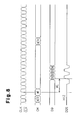
- FIG. 8 is a timing diagram showing the write operation of the DDR-SDRAM of FIG. 3 .
- FIG. 3 is a schematic block diagram of a DDR-SDRAM 200 according to one embodiment of the present invention.
- the DDR-SDRAM 200 comprises three input circuits 1 a , 1 b and 1 c , two FIFO memories 11 a and 11 b , a first-stage control circuit 12 , a precoder 3 , a main decoder 4 , a sense amplifier 5 , a control circuit 6 , a write amplifier 7 and a memory cell array 10 .
- Read latency RL of the DDR-SDRAM 200 is set according to a frequency of a clock signal CLK, and is set to “2” or “3” as the frequency increases.
- the read latency RL is set to “3” and write latency WL is set to “2” (RL “3” ⁇ 1).
- the read latency RL is the latency period until a read operation is started after a read command has been supplied.
- the write latency WL is the latency period until write data DQ is supplied after a write command WR has been supplied.
- the FIFO memories 11 a , 11 b delay the output signals from the input circuits 1 a , 1 b in accordance with the write latency WL “2” by two cycles of the clock signal CLK and outputs delayed signals.
- the input circuit 1 b comprise four input circuits 13 a to 13 d that receive control signals /CS, /RAS, /CAS and /WE respectively and supply delayed control signals to the FIFO memory 11 b.
- the input circuit 1 c includes a differential circuit shown in FIG. 6 . That is, an input signal in (i.e., write data DQ) and a reference voltage Vref are supplied to the gates of a pair of N-channel MOS transistors Tr 1 , Tr 2 , respectively.
- the sources of the transistors Tr 1 , Tr 2 are connected to the drain of an N-channel MOS transistor Tr 3 and the source of the transistor Tr 3 is connected to a low potential power supply Vss.
- the input circuits 1 a and 13 a to 13 d have the same circuit configuration as the input circuit 1 c.
- the drain of the transistor Tr 1 is connected to the drains of P-channel MOS transistors Tr 4 , Tr 5 and a high potential power supply VDD is connected to the sources of the transistors Tr 4 , Tr 5 .
- the drain of the transistor Tr 2 is connected to the drains of P-channel MOS transistors Tr 6 , Tr 7 and the high potential power supply VDD is connected to the sources of the transistors Tr 6 , Tr 7 .
- the gates of the transistors Tr 5 , Tr 6 are connected together and to the drain of the transistor Tr 2 .
- An activation signal enb is supplied to the gates of the transistors Tr 3 , Tr 4 and Tr 7 via an inverter circuit 14 a.
- the voltage of the drain (node N 1 ) of the transistor Tr 1 is output via three inverter circuits 14 c to 14 e as an output signal outz and is output via the two inverter circuits 14 c and 14 d as an output signal outx.
- the transistor Tr 3 when the activation signal enb goes high, the transistor Tr 3 is turned off and the transistors Tr 4 , Tr 7 are turned on. Accordingly, regardless of the level of the input signal in, the node N 1 is fixed to a high level voltage, the output signal outz is fixed to a low level, and the output signal outx is fixed to the H level.
- the activation signal enb goes low, the transistor Tr 3 is turned on, the transistors Tr 4 , Tr 7 are turned off, and the input circuit 1 c is activated.
- the node N 1 When the voltage of the input signal in is higher than the reference voltage Vref, the node N 1 is set to the L level and the output signal outz having the H level and the output signal outx having the L level are output. When the voltage of the input signal in is lower than the reference voltage Vref, the node N 1 is set to the H level and the output signal outz having the L level and the output signal outx having the H level are output.
- FIG. 4 is a schematic circuit diagram of the first-stage control circuit 12 and FIG. 5 is a schematic circuit diagram of an internal circuit of the first stage control circuit 12 .
- the output signal outx of the input circuit 13 a and the output signal outz of the input circuit 13 b are supplied to a NAND circuit 15 a .
- the output signal outx of the input circuit 13 c and the output signal outx of the input circuit 13 d are supplied to a NAND circuit 15 b .
- the output signals of the NAND circuits 15 a , 15 b are supplied to a NOR circuit 16 . Accordingly, the NOR circuit 16 outputs an output signal having the H level when the input signals of the NAND circuits 15 a , 15 b go high, that is, when a write command WR is supplied.
- the output terminal (node N 2 ) of the NOR circuit 16 is connected to the gate of an N-channel MOS transistor Tr 8 and to the gate of an N-channel MOS transistor Tr 9 via an inverter circuit 14 f .
- the drain of the transistor Tr 8 is connected to the drain of a P-channel MOS transistor Tr 10 and the source of the transistor Tr 10 is connected to the high potential power supply VDD.
- the drain of the transistor Tr 9 is connected to the drain of a P-channel MOS transistor Tr 11 and the source of the transistor Tr 11 is connected to the high potential power supply VDD.
- the source of the transistor Tr 8 is connected to the low potential power supply Vss via N-channel MOS transistors Tr 12 , Tr 13 and the source of the transistor Tr 9 is connected to the low potential power supply Vss via N-channel MOS transistors Tr 14 , Tr 15 . Further, the sources of the transistors Tr 8 , Tr 9 are connected to each other via an N-channel MOS transistor Tr 16 .
- a node N 4 at the drains of the transistors Tr 8 , Tr 10 is connected to the drains of an N-channel MOS transistor Tr 17 and a P-channel MOS transistor Tr 18 and is connected to the gates of an N-channel MOS transistor Tr 19 and a P-channel MOS transistor Tr 20 .
- the drains of the transistors Tr 17 , Tr 18 are connected together and the drains of the transistors Tr 19 , Tr 20 are mutually connected.
- the sources of the transistors Tr 18 , Tr 20 are connected to the high potential power supply VDD.
- the drains (node N 3 ) of the transistors Tr 9 , Tr 11 are connected to the drains of the transistors Tr 19 , Tr 20 and the gates of the transistors Tr 17 , Tr 18 .
- a clock signal CLK is supplied to the gates of the transistors Tr 10 , Tr 11 , Tr 12 and Tr 14 via two inverter circuits 14 g and 14 h .
- the clock signal CLK is also supplied to the gates of the transistors Tr 13 , Tr 15 and Tr 16 via the inverter circuit 14 g and two inverter circuits 14 i , 14 j .
- the clock signal CLK is supplied to the sources of the transistors Tr 17 , Tr 19 via the inverter circuit 14 g , 14 i and 14 j .
- the transistors Tr 17 to Tr 20 enlarge the potential difference between the nodes N 3 , N 4 and cause the rising and falling of voltages of the nodes N 3 , N 4 to be faster.
- the voltage of the node N 3 is supplied to the gate of a P-channel MOS transistor Tr 2 l and to the gate of an N-channel MOS transistor Tr 22 via the inverter circuit 14 k .
- the voltage of node N 4 is supplied to the gate of a P-channel MOS transistor Tr 24 and to the gate of an N-channel MOS transistor Tr 23 via an inverter circuit 14 m.
- the sources of the transistors Tr 21 , Tr 24 are connected to the high potential power supply VDD and the sources of the transistors Tr 23 , Tr 22 are connected to the low potential power supply Vss.
- a signal wrtb is output from the drains of the transistors Tr 21 , Tr 23 and a signal wrt is output from the drains of the transistors Tr 24 , Tr 22 .
- a latch circuit 17 a is connected between the drains of the transistors Tr 21 , Tr 23 and the drains of the transistors Tr 24 , Tr 22 .
- the signal wrtb is supplied to a NAND circuit 15 c and the output signal of the NAND circuit 15 c is supplied to a NAND circuit 15 d .
- a reset signal rstb is supplied from an external device to the NAND circuit 15 d .
- the reset signal rstb is a one-shot pulse signal which falls from high to low when the termination of the write operation is detected based on the control signals /CS, /RAS, /CAS and /WE.
- the output of the NAND circuit 15 d is supplied to the NAND circuit 15 c.
- the output signal of the NAND circuit 15 c is supplied to a transfer gate 18 a via an inverter circuit 14 n .
- the transfer signal of the transfer gate 18 a is supplied to a latch circuit 17 b and the latch signal of the latch circuit 17 b is supplied to a transfer gate 18 b .
- the transfer signal of the transfer gate 18 b is supplied to a latch circuit 17 c and the latch signal of the latch circuit 17 c is supplied to a transfer gate 18 c .
- the transfer signal of the transfer gate 18 c is supplied to a latch circuit 17 d and the latch signal of the latch circuit 17 d is supplied to a transfer gate 18 d .
- the transfer signal of the transfer gate 18 d is supplied to a latch circuit 17 e and the latch signal (node N 7 ) of the latch circuit 17 e is supplied to a NAND circuit 15 e .
- the output signal (node N 5 ) of the inverter circuit 14 n and the latch signal (node N 6 ) of the latch circuit 17 c are also supplied to the NAND circuit 15 e .
- the output signal of the NAND circuit 15 e is supplied to the input circuit 1 c via an inverter circuit 14 p as an activation signal enb.
- Each of the transfer gates 18 a to 18 d operates in response to a signal having the same phase as the clock signal CLK and an inverse signal of the clock signal CLK. That is, the transfer gates 18 a , 18 c and the transfer gates 18 b , 18 d are conductive alternatively in accordance with an equi-phase signal and an inverse signal.
- the transistors Tr 10 , Tr 11 are intermittently turned on by the clock signal CLK.
- the transistors Tr 12 , Tr 13 and the transistors Tr 14 , Tr 15 are turned on during the operation delay time of one inverter circuit, so that the sources of the transistors Tr 8 , Tr 9 and the low potential power supply Vss are connected.
- the node N 4 is fixed to the H level and an inverse signal of the clock signal CLK is generated at the node N 3 .
- the transistors Tr 21 , Tr 22 , Tr 23 and Tr 24 are all turned off or only the transistors Tr 21 , Tr 22 are turned on, so that a command decision signal wrtb having the H level and a command decision signal wrt having the L level are maintained by the latch circuit 17 a.
- the NAND circuit 15 c When the command decision signal wrtb is high, the NAND circuit 15 c outputs an output signal maintained at the L level in response to a reset signal rstb at the preceding cycle. Then, the output signal of the inverter circuit 14 n is maintained at the H level and signals having the H level are supplied to the NAND circuit 15 e . Accordingly, an activation signal enb having the H level is output from the inverter circuit 14 p and the third input circuit 1 c is maintained in an inactive state.
- the command decision signal wrtb falls and the command decision signal wrt rises.
- the command decision signals wrtb, wrt are maintained high and low, respectively, until the node N 3 falls again.
- the activation signal enb falls in response to the falling edge of the command decision signal wrtb.
- the node N 5 falls in response to the falling edge of the command decision signal wrtb.
- the node N 6 falls one clock after the falling edge of the node N 5 and the node N 7 falls one clock after the falling edge of the node N 6 .
- the node N 5 returns to the H level.
- the node N 6 returns to the H level after one clock and subsequently the node N 7 returns to the H level after one clock.
- Such operation allows the activation signal enb to be maintained at the L level until the node N 7 rises after the node N 5 has fallen, and the third input circuit 1 c to be activated by the activation signal enb.
- the read latency RL is set to “3”.
- a write command WR is supplied from an external device following a word line selection command ACTV.
- the write command WR is set by setting the control signals /CS, /RAS, /CAS and /WE at predetermined levels.
- the latency until the write command WR is supplied after the word line activation command ACTV has been supplied is shorter than the latency until a read command is supplied after the word line activation command ACTV has been supplied.
- the third input circuit 1 c is activated by the first-stage control circuit 12 .
- an I/O control signal DQS and write data DQ are supplied from the external device and the write data DQ is acquired by the activated third input circuit 1 c.
- An address signal AD supplied to the first input circuit 1 a is supplied to the predecoder 3 via the FIFO memory 11 a .
- a predecode signal of the predecoder 3 is supplied to the main decoder 4 .
- a write command WR supplied to the second input circuit 1 b is supplied to the control circuit 6 via the FIFO memory 11 b .
- the write amplifier 7 and the main decoder 4 are activated by the output signal of the control circuit 6 and the sense amplifier 5 is activated based on the operation of the main decoder 4 .
- the write amplifier 7 and the sense amplifier 5 are activated and the write data DQ is written to a memory cell selected in accordance with the address signal AD in units of two bits.
- the DDR-SDRAM 200 has the following advantages.
- the write latency WL is set to “2” which is one lower than read latency RL “3”. That is, the write latency WL is set to RL ⁇ 1. Accordingly, the time until the write operation is completed after a word line activation command ACTV has been supplied is decreased without setting the write latency WL longer than necessary while activating the third input circuit 1 c in accordance with a write command WR.
- the latency until a write command WR is supplied after a word line activation command ACTV has been supplied is set shorter than the latency until a read command is supplied after the word line activation command ACTV has been supplied. Accordingly, even if the write latency WL is set relatively long, the time from the supply of the word line activation command ACTV to the completion of the write operation is decreased. That is, the elongation of write latency is canceled by the latency from the supply of the word line activation command ACTV to the supply of the write command WR.
Abstract
Description
Claims (12)
Applications Claiming Priority (2)
| Application Number | Priority Date | Filing Date | Title |
|---|---|---|---|
| JP11-326876 | 1999-11-17 | ||
| JP32687699A JP4421036B2 (en) | 1999-11-17 | 1999-11-17 | Data writing method for semiconductor memory device and semiconductor memory device |
Publications (1)
| Publication Number | Publication Date |
|---|---|
| US6310825B1 true US6310825B1 (en) | 2001-10-30 |
Family
ID=18192734
Family Applications (1)
| Application Number | Title | Priority Date | Filing Date |
|---|---|---|---|
| US09/671,647 Expired - Lifetime US6310825B1 (en) | 1999-11-17 | 2000-09-28 | Data writing method for semiconductor memory device |
Country Status (3)
| Country | Link |
|---|---|
| US (1) | US6310825B1 (en) |
| JP (1) | JP4421036B2 (en) |
| TW (1) | TW578152B (en) |
Cited By (8)
| Publication number | Priority date | Publication date | Assignee | Title |
|---|---|---|---|---|
| US20040114448A1 (en) * | 2002-12-11 | 2004-06-17 | Johnson Christopher S. | Memory device and method having low-power, high write latency mode and high-power, low write latency mode and/or independently selectable write latency |
| US20060158949A1 (en) * | 2004-07-15 | 2006-07-20 | Klein Dean A | Method and system for controlling refresh to avoid memory cell data losses |
| US7099221B2 (en) | 2004-05-06 | 2006-08-29 | Micron Technology, Inc. | Memory controller method and system compensating for memory cell data losses |
| US7184352B2 (en) | 2004-08-31 | 2007-02-27 | Micron Technology, Inc. | Memory system and method using ECC to achieve low power refresh |
| US7340668B2 (en) | 2004-06-25 | 2008-03-04 | Micron Technology, Inc. | Low power cost-effective ECC memory system and method |
| US7461320B2 (en) | 2004-06-24 | 2008-12-02 | Micron Technology, Inc. | Memory system and method having selective ECC during low power refresh |
| US7894289B2 (en) | 2006-10-11 | 2011-02-22 | Micron Technology, Inc. | Memory system and method using partial ECC to achieve low power refresh and fast access to data |
| US7900120B2 (en) | 2006-10-18 | 2011-03-01 | Micron Technology, Inc. | Memory system and method using ECC with flag bit to identify modified data |
Citations (4)
| Publication number | Priority date | Publication date | Assignee | Title |
|---|---|---|---|---|
| US5568445A (en) * | 1994-03-03 | 1996-10-22 | Samsung Electronics Co., Ltd. | Synchronous semiconductor memory device with a write latency control function |
| US5793688A (en) * | 1995-06-30 | 1998-08-11 | Micron Technology, Inc. | Method for multiple latency synchronous dynamic random access memory |
| US5966343A (en) * | 1997-01-02 | 1999-10-12 | Texas Instruments Incorporated | Variable latency memory circuit |
| US6215722B1 (en) * | 1998-12-30 | 2001-04-10 | Hyundai Electronics Industries Co., Ltd. | Command latency circuit for programmable SLDRAM and latency control method therefor |
-
1999
- 1999-11-17 JP JP32687699A patent/JP4421036B2/en not_active Expired - Lifetime
-
2000
- 2000-09-13 TW TW089118703A patent/TW578152B/en not_active IP Right Cessation
- 2000-09-28 US US09/671,647 patent/US6310825B1/en not_active Expired - Lifetime
Patent Citations (6)
| Publication number | Priority date | Publication date | Assignee | Title |
|---|---|---|---|---|
| US5568445A (en) * | 1994-03-03 | 1996-10-22 | Samsung Electronics Co., Ltd. | Synchronous semiconductor memory device with a write latency control function |
| US5793688A (en) * | 1995-06-30 | 1998-08-11 | Micron Technology, Inc. | Method for multiple latency synchronous dynamic random access memory |
| US5813023A (en) * | 1995-06-30 | 1998-09-22 | Micron Technology, Inc. | Method and apparatus for multiple latency synchronous dynamic random access memory |
| US6130856A (en) * | 1995-06-30 | 2000-10-10 | Micron Technology, Inc. | Method and apparatus for multiple latency synchronous dynamic random access memory |
| US5966343A (en) * | 1997-01-02 | 1999-10-12 | Texas Instruments Incorporated | Variable latency memory circuit |
| US6215722B1 (en) * | 1998-12-30 | 2001-04-10 | Hyundai Electronics Industries Co., Ltd. | Command latency circuit for programmable SLDRAM and latency control method therefor |
Cited By (49)
| Publication number | Priority date | Publication date | Assignee | Title |
|---|---|---|---|---|
| US7254067B2 (en) | 2002-12-11 | 2007-08-07 | Micron Technology, Inc. | Memory device and method having low-power, high write latency mode and high-power, low write latency mode and/or independently selectable write latency |
| US20070268756A1 (en) * | 2002-12-11 | 2007-11-22 | Johnson Christopher S | Memory device and method having low-power, high write latency mode and high-power, low write latency mode and/or independently selectable write latency |
| US20050122797A1 (en) * | 2002-12-11 | 2005-06-09 | Johnson Christopher S. | Memory device and method having low-power, high write latency mode and high-power, low write latency mode and/or independently selectable write latency |
| WO2004053879A3 (en) * | 2002-12-11 | 2005-07-07 | Micron Technology Inc | Memory device and method having low-power, high write latency mode and high-power, low write latency mode and/or independently selectable write latency |
| US6934199B2 (en) * | 2002-12-11 | 2005-08-23 | Micron Technology, Inc. | Memory device and method having low-power, high write latency mode and high-power, low write latency mode and/or independently selectable write latency |
| US7027337B2 (en) | 2002-12-11 | 2006-04-11 | Micron Technology, Inc. | Memory device and method having low-power, high write latency mode and high-power, low write latency mode and/or independently selectable write latency |
| US20060152983A1 (en) * | 2002-12-11 | 2006-07-13 | Johnson Christopher S | Memory device and method having low-power, high write latency mode and high-power, low write latency mode and/or independently selectable write latency |
| US7149141B2 (en) | 2002-12-11 | 2006-12-12 | Micron Technology, Inc. | Memory device and method having low-power, high write latency mode and high-power, low write latency mode and/or independently selectable write latency |
| US7450447B2 (en) | 2002-12-11 | 2008-11-11 | Micron Technology, Inc. | Memory device and method having low-power, high write latency mode and high-power, low write latency mode and/or independently selectable write latency |
| US8164965B2 (en) | 2002-12-11 | 2012-04-24 | Round Rock Research, Llc | Memory device and method having low-power, high write latency mode and high-power, low write latency mode and/or independently selectable write latency |
| CN1748261B (en) * | 2002-12-11 | 2010-05-26 | 米克伦技术公司 | Method and device write latency control of memory |
| US7826283B2 (en) | 2002-12-11 | 2010-11-02 | Round Rock Research, Llc | Memory device and method having low-power, high write latency mode and high-power, low write latency mode and/or independently selectable write latency |
| US20110038217A1 (en) * | 2002-12-11 | 2011-02-17 | Round Rock Research, Llc | Memory device and method having low-power, high write latency mode and high-power, low write latency mode and/or independently selectable write latency |
| US20050117414A1 (en) * | 2002-12-11 | 2005-06-02 | Johnson Christopher S. | Memory device and method having low-power, high write latency mode and high-power, low write latency mode and/or independently selectable write latency |
| US20040114448A1 (en) * | 2002-12-11 | 2004-06-17 | Johnson Christopher S. | Memory device and method having low-power, high write latency mode and high-power, low write latency mode and/or independently selectable write latency |
| US7836374B2 (en) | 2004-05-06 | 2010-11-16 | Micron Technology, Inc. | Memory controller method and system compensating for memory cell data losses |
| US20110060961A1 (en) * | 2004-05-06 | 2011-03-10 | Micro Technology, Inc. | Memory controller method and system compensating for memory cell data losses |
| US7447974B2 (en) | 2004-05-06 | 2008-11-04 | Micron Technology, Inc. | Memory controller method and system compensating for memory cell data losses |
| US7428687B2 (en) | 2004-05-06 | 2008-09-23 | Micron Technology, Inc. | Memory controller method and system compensating for memory cell data losses |
| US7447973B2 (en) | 2004-05-06 | 2008-11-04 | Micron Technology, Inc. | Memory controller method and system compensating for memory cell data losses |
| US8689077B2 (en) | 2004-05-06 | 2014-04-01 | Micron Technology, Inc. | Memory controller method and system compensating for memory cell data losses |
| US7099221B2 (en) | 2004-05-06 | 2006-08-29 | Micron Technology, Inc. | Memory controller method and system compensating for memory cell data losses |
| US9064600B2 (en) | 2004-05-06 | 2015-06-23 | Micron Technology, Inc. | Memory controller method and system compensating for memory cell data losses |
| US7461320B2 (en) | 2004-06-24 | 2008-12-02 | Micron Technology, Inc. | Memory system and method having selective ECC during low power refresh |
| US7526713B2 (en) | 2004-06-25 | 2009-04-28 | Micron Technology, Inc. | Low power cost-effective ECC memory system and method |
| US7340668B2 (en) | 2004-06-25 | 2008-03-04 | Micron Technology, Inc. | Low power cost-effective ECC memory system and method |
| US20110134708A1 (en) * | 2004-07-15 | 2011-06-09 | Micron Technology, Inc. | Method and system for controlling refresh to avoid memory cell data losses |
| US20060158949A1 (en) * | 2004-07-15 | 2006-07-20 | Klein Dean A | Method and system for controlling refresh to avoid memory cell data losses |
| US7558142B2 (en) | 2004-07-15 | 2009-07-07 | Micron Technology, Inc. | Method and system for controlling refresh to avoid memory cell data losses |
| US7623392B2 (en) | 2004-07-15 | 2009-11-24 | Micron Technology, Inc. | Method and system for controlling refresh to avoid memory cell data losses |
| US7280386B2 (en) | 2004-07-15 | 2007-10-09 | Micron Technology, Inc. | Method and system for controlling refresh to avoid memory cell data losses |
| US7277345B2 (en) | 2004-07-15 | 2007-10-02 | Micron Technology, Inc. | Method and system for controlling refresh to avoid memory cell data losses |
| US20100054070A1 (en) * | 2004-07-15 | 2010-03-04 | Micron Technology, Inc. | Method and system for controlling refresh to avoid memory cell data losses |
| US8446783B2 (en) | 2004-07-15 | 2013-05-21 | Micron Technology, Inc. | Digit line comparison circuits |
| US7898892B2 (en) | 2004-07-15 | 2011-03-01 | Micron Technology, Inc. | Method and system for controlling refresh to avoid memory cell data losses |
| US8279683B2 (en) | 2004-07-15 | 2012-10-02 | Micron Technology, Inc. | Digit line comparison circuits |
| US20080151671A1 (en) * | 2004-07-15 | 2008-06-26 | Micron Technology, Inc. | Method and system for controlling refresh to avoid memory cell data losses |
| US7116602B2 (en) | 2004-07-15 | 2006-10-03 | Micron Technology, Inc. | Method and system for controlling refresh to avoid memory cell data losses |
| US7272066B2 (en) | 2004-07-15 | 2007-09-18 | Micron Technology, Inc. | Method and system for controlling refresh to avoid memory cell data losses |
| US7184352B2 (en) | 2004-08-31 | 2007-02-27 | Micron Technology, Inc. | Memory system and method using ECC to achieve low power refresh |
| US7894289B2 (en) | 2006-10-11 | 2011-02-22 | Micron Technology, Inc. | Memory system and method using partial ECC to achieve low power refresh and fast access to data |
| US8359517B2 (en) | 2006-10-11 | 2013-01-22 | Micron Technology, Inc. | Memory system and method using partial ECC to achieve low power refresh and fast access to data |
| US9286161B2 (en) | 2006-10-11 | 2016-03-15 | Micron Technology, Inc. | Memory system and method using partial ECC to achieve low power refresh and fast access to data |
| US8832522B2 (en) | 2006-10-11 | 2014-09-09 | Micron Technology, Inc. | Memory system and method using partial ECC to achieve low power refresh and fast access to data |
| US8413007B2 (en) | 2006-10-18 | 2013-04-02 | Micron Technology, Inc. | Memory system and method using ECC with flag bit to identify modified data |
| US8601341B2 (en) | 2006-10-18 | 2013-12-03 | Micron Technologies, Inc. | Memory system and method using ECC with flag bit to identify modified data |
| US8880974B2 (en) | 2006-10-18 | 2014-11-04 | Micron Technology, Inc. | Memory system and method using ECC with flag bit to identify modified data |
| US7900120B2 (en) | 2006-10-18 | 2011-03-01 | Micron Technology, Inc. | Memory system and method using ECC with flag bit to identify modified data |
| US20110138252A1 (en) * | 2006-10-18 | 2011-06-09 | Pawlowski J Thomas | Memory system and method using ecc with flag bit to identify modified data |
Also Published As
| Publication number | Publication date |
|---|---|
| JP2001143468A (en) | 2001-05-25 |
| JP4421036B2 (en) | 2010-02-24 |
| TW578152B (en) | 2004-03-01 |
Similar Documents
| Publication | Publication Date | Title |
|---|---|---|
| US6424590B1 (en) | Semiconductor device | |
| US6804158B2 (en) | Semiconductor circuit device with improved special mode | |
| US10872646B2 (en) | Apparatuses and methods for providing active and inactive clock signals | |
| JP3341710B2 (en) | Semiconductor storage device | |
| US7283421B2 (en) | Semiconductor memory device | |
| US6885606B2 (en) | Synchronous semiconductor memory device with a plurality of memory banks and method of controlling the same | |
| US6789137B2 (en) | Semiconductor memory device allowing reduction of I/O terminals | |
| US6636443B2 (en) | Semiconductor memory device having row buffers | |
| US20030031081A1 (en) | Semiconductor memory device operating in synchronization with data strobe signal | |
| JP4762520B2 (en) | Semiconductor integrated circuit | |
| US6310825B1 (en) | Data writing method for semiconductor memory device | |
| JPH10162576A (en) | Column selection line enable circuit for semiconductor memory device | |
| US5909407A (en) | Word line multi-selection circuit for a memory device | |
| US6992949B2 (en) | Method and circuit for controlling generation of column selection line signal | |
| US6341100B1 (en) | Semiconductor integrated circuit having circuit for writing data to memory cell | |
| JP3447640B2 (en) | Semiconductor storage device | |
| CN110998732B (en) | Input buffer circuit | |
| US6608797B1 (en) | Automatic delay technique for early read and write operations in synchronous dynamic random access memories | |
| US11366487B2 (en) | Resetting clock divider circuitry prior to a clock restart | |
| JPH05128857A (en) | Semiconductor memory |
Legal Events
| Date | Code | Title | Description |
|---|---|---|---|
| AS | Assignment |
Owner name: FUJITSU LIMITED, JAPAN Free format text: ASSIGNMENT OF ASSIGNORS INTEREST;ASSIGNOR:FURUYAMA, TAKAAKI;REEL/FRAME:011161/0849 Effective date: 20000829 |
|
| STCF | Information on status: patent grant |
Free format text: PATENTED CASE |
|
| CC | Certificate of correction | ||
| FEPP | Fee payment procedure |
Free format text: PAYOR NUMBER ASSIGNED (ORIGINAL EVENT CODE: ASPN); ENTITY STATUS OF PATENT OWNER: LARGE ENTITY |
|
| FPAY | Fee payment |
Year of fee payment: 4 |
|
| AS | Assignment |
Owner name: FUJITSU MICROELECTRONICS LIMITED, JAPAN Free format text: ASSIGNMENT OF ASSIGNORS INTEREST;ASSIGNOR:FUJITSU LIMITED;REEL/FRAME:021998/0645 Effective date: 20081104 Owner name: FUJITSU MICROELECTRONICS LIMITED,JAPAN Free format text: ASSIGNMENT OF ASSIGNORS INTEREST;ASSIGNOR:FUJITSU LIMITED;REEL/FRAME:021998/0645 Effective date: 20081104 |
|
| FPAY | Fee payment |
Year of fee payment: 8 |
|
| AS | Assignment |
Owner name: FUJITSU SEMICONDUCTOR LIMITED, JAPAN Free format text: CHANGE OF NAME;ASSIGNOR:FUJITSU MICROELECTRONICS LIMITED;REEL/FRAME:024982/0245 Effective date: 20100401 |
|
| CC | Certificate of correction | ||
| CC | Certificate of correction | ||
| FPAY | Fee payment |
Year of fee payment: 12 |
|
| AS | Assignment |
Owner name: SOCIONEXT INC., JAPAN Free format text: ASSIGNMENT OF ASSIGNORS INTEREST;ASSIGNOR:FUJITSU SEMICONDUCTOR LIMITED;REEL/FRAME:035508/0637 Effective date: 20150302 |