US6312997B1 - Low voltage high performance semiconductor devices and methods - Google Patents
Low voltage high performance semiconductor devices and methods Download PDFInfo
- Publication number
- US6312997B1 US6312997B1 US09/132,904 US13290498A US6312997B1 US 6312997 B1 US6312997 B1 US 6312997B1 US 13290498 A US13290498 A US 13290498A US 6312997 B1 US6312997 B1 US 6312997B1
- Authority
- US
- United States
- Prior art keywords
- dopant
- conductivity type
- active region
- implanting
- gate structure
- Prior art date
- Legal status (The legal status is an assumption and is not a legal conclusion. Google has not performed a legal analysis and makes no representation as to the accuracy of the status listed.)
- Expired - Fee Related
Links
- 238000000034 method Methods 0.000 title claims abstract description 65
- 239000004065 semiconductor Substances 0.000 title claims abstract description 37
- 239000007943 implant Substances 0.000 claims abstract description 95
- 230000003071 parasitic effect Effects 0.000 claims abstract description 12
- 230000000694 effects Effects 0.000 claims abstract description 8
- 239000002019 doping agent Substances 0.000 claims description 92
- 239000000758 substrate Substances 0.000 claims description 27
- XUIMIQQOPSSXEZ-UHFFFAOYSA-N Silicon Chemical compound [Si] XUIMIQQOPSSXEZ-UHFFFAOYSA-N 0.000 claims description 24
- 229910052710 silicon Inorganic materials 0.000 claims description 24
- 239000010703 silicon Substances 0.000 claims description 24
- 125000006850 spacer group Chemical group 0.000 claims description 19
- 230000015572 biosynthetic process Effects 0.000 claims description 15
- ZOXJGFHDIHLPTG-UHFFFAOYSA-N Boron Chemical compound [B] ZOXJGFHDIHLPTG-UHFFFAOYSA-N 0.000 claims description 12
- 229910052796 boron Inorganic materials 0.000 claims description 12
- 238000004519 manufacturing process Methods 0.000 claims description 7
- 230000000149 penetrating effect Effects 0.000 claims description 5
- BHEPBYXIRTUNPN-UHFFFAOYSA-N hydridophosphorus(.) (triplet) Chemical compound [PH] BHEPBYXIRTUNPN-UHFFFAOYSA-N 0.000 claims description 3
- 238000002513 implantation Methods 0.000 claims description 2
- 238000000137 annealing Methods 0.000 claims 1
- 230000002265 prevention Effects 0.000 abstract description 12
- 230000008569 process Effects 0.000 description 18
- VYPSYNLAJGMNEJ-UHFFFAOYSA-N Silicium dioxide Chemical compound O=[Si]=O VYPSYNLAJGMNEJ-UHFFFAOYSA-N 0.000 description 9
- OAICVXFJPJFONN-UHFFFAOYSA-N Phosphorus Chemical compound [P] OAICVXFJPJFONN-UHFFFAOYSA-N 0.000 description 7
- 229910052698 phosphorus Inorganic materials 0.000 description 7
- 239000011574 phosphorus Substances 0.000 description 7
- 238000012545 processing Methods 0.000 description 7
- 229910052785 arsenic Inorganic materials 0.000 description 6
- RQNWIZPPADIBDY-UHFFFAOYSA-N arsenic atom Chemical compound [As] RQNWIZPPADIBDY-UHFFFAOYSA-N 0.000 description 6
- 238000002955 isolation Methods 0.000 description 6
- 229910052581 Si3N4 Inorganic materials 0.000 description 5
- 229920002120 photoresistant polymer Polymers 0.000 description 5
- 229910021420 polycrystalline silicon Inorganic materials 0.000 description 5
- FVBUAEGBCNSCDD-UHFFFAOYSA-N silicide(4-) Chemical compound [Si-4] FVBUAEGBCNSCDD-UHFFFAOYSA-N 0.000 description 5
- 238000005229 chemical vapour deposition Methods 0.000 description 4
- 238000000151 deposition Methods 0.000 description 4
- 230000008021 deposition Effects 0.000 description 4
- 239000012535 impurity Substances 0.000 description 4
- 239000000377 silicon dioxide Substances 0.000 description 4
- HQVNEWCFYHHQES-UHFFFAOYSA-N silicon nitride Chemical compound N12[Si]34N5[Si]62N3[Si]51N64 HQVNEWCFYHHQES-UHFFFAOYSA-N 0.000 description 4
- XAGFODPZIPBFFR-UHFFFAOYSA-N aluminium Chemical compound [Al] XAGFODPZIPBFFR-UHFFFAOYSA-N 0.000 description 3
- 238000009792 diffusion process Methods 0.000 description 3
- 238000005468 ion implantation Methods 0.000 description 3
- 150000004767 nitrides Chemical class 0.000 description 3
- 229920005591 polysilicon Polymers 0.000 description 3
- 229910021332 silicide Inorganic materials 0.000 description 3
- 235000012239 silicon dioxide Nutrition 0.000 description 3
- 229910052782 aluminium Inorganic materials 0.000 description 2
- 230000008901 benefit Effects 0.000 description 2
- 230000015556 catabolic process Effects 0.000 description 2
- 239000002800 charge carrier Substances 0.000 description 2
- 230000005684 electric field Effects 0.000 description 2
- 230000000873 masking effect Effects 0.000 description 2
- 239000000463 material Substances 0.000 description 2
- 229910052751 metal Inorganic materials 0.000 description 2
- 239000002184 metal Substances 0.000 description 2
- 230000003647 oxidation Effects 0.000 description 2
- 238000007254 oxidation reaction Methods 0.000 description 2
- WQJQOUPTWCFRMM-UHFFFAOYSA-N tungsten disilicide Chemical compound [Si]#[W]#[Si] WQJQOUPTWCFRMM-UHFFFAOYSA-N 0.000 description 2
- 229910021342 tungsten silicide Inorganic materials 0.000 description 2
- 238000013459 approach Methods 0.000 description 1
- 230000004888 barrier function Effects 0.000 description 1
- 239000005380 borophosphosilicate glass Substances 0.000 description 1
- 229910052681 coesite Inorganic materials 0.000 description 1
- 230000002860 competitive effect Effects 0.000 description 1
- 239000004020 conductor Substances 0.000 description 1
- 238000010276 construction Methods 0.000 description 1
- 229910052906 cristobalite Inorganic materials 0.000 description 1
- 239000013078 crystal Substances 0.000 description 1
- 230000001419 dependent effect Effects 0.000 description 1
- 238000005137 deposition process Methods 0.000 description 1
- 238000013461 design Methods 0.000 description 1
- 238000005516 engineering process Methods 0.000 description 1
- 230000008020 evaporation Effects 0.000 description 1
- 238000001704 evaporation Methods 0.000 description 1
- 239000012634 fragment Substances 0.000 description 1
- 239000011521 glass Substances 0.000 description 1
- 150000002500 ions Chemical class 0.000 description 1
- 238000012986 modification Methods 0.000 description 1
- 230000004048 modification Effects 0.000 description 1
- 238000002161 passivation Methods 0.000 description 1
- 238000000059 patterning Methods 0.000 description 1
- 238000005498 polishing Methods 0.000 description 1
- 230000009467 reduction Effects 0.000 description 1
- 229910052814 silicon oxide Inorganic materials 0.000 description 1
- 238000004544 sputter deposition Methods 0.000 description 1
- 239000007858 starting material Substances 0.000 description 1
- 229910052682 stishovite Inorganic materials 0.000 description 1
- 239000000126 substance Substances 0.000 description 1
- 229910052905 tridymite Inorganic materials 0.000 description 1
- WFKWXMTUELFFGS-UHFFFAOYSA-N tungsten Chemical compound [W] WFKWXMTUELFFGS-UHFFFAOYSA-N 0.000 description 1
- 229910052721 tungsten Inorganic materials 0.000 description 1
- 239000010937 tungsten Substances 0.000 description 1
Images


Classifications
-
- H—ELECTRICITY
- H01—ELECTRIC ELEMENTS
- H01L—SEMICONDUCTOR DEVICES NOT COVERED BY CLASS H10
- H01L29/00—Semiconductor devices adapted for rectifying, amplifying, oscillating or switching, or capacitors or resistors with at least one potential-jump barrier or surface barrier, e.g. PN junction depletion layer or carrier concentration layer; Details of semiconductor bodies or of electrodes thereof ; Multistep manufacturing processes therefor
- H01L29/66—Types of semiconductor device ; Multistep manufacturing processes therefor
- H01L29/66007—Multistep manufacturing processes
- H01L29/66075—Multistep manufacturing processes of devices having semiconductor bodies comprising group 14 or group 13/15 materials
- H01L29/66227—Multistep manufacturing processes of devices having semiconductor bodies comprising group 14 or group 13/15 materials the devices being controllable only by the electric current supplied or the electric potential applied, to an electrode which does not carry the current to be rectified, amplified or switched, e.g. three-terminal devices
- H01L29/66409—Unipolar field-effect transistors
- H01L29/66477—Unipolar field-effect transistors with an insulated gate, i.e. MISFET
- H01L29/66537—Unipolar field-effect transistors with an insulated gate, i.e. MISFET using a self aligned punch through stopper or threshold implant under the gate region
-
- H—ELECTRICITY
- H01—ELECTRIC ELEMENTS
- H01L—SEMICONDUCTOR DEVICES NOT COVERED BY CLASS H10
- H01L21/00—Processes or apparatus adapted for the manufacture or treatment of semiconductor or solid state devices or of parts thereof
- H01L21/02—Manufacture or treatment of semiconductor devices or of parts thereof
- H01L21/04—Manufacture or treatment of semiconductor devices or of parts thereof the devices having at least one potential-jump barrier or surface barrier, e.g. PN junction, depletion layer or carrier concentration layer
- H01L21/18—Manufacture or treatment of semiconductor devices or of parts thereof the devices having at least one potential-jump barrier or surface barrier, e.g. PN junction, depletion layer or carrier concentration layer the devices having semiconductor bodies comprising elements of Group IV of the Periodic System or AIIIBV compounds with or without impurities, e.g. doping materials
- H01L21/26—Bombardment with radiation
- H01L21/263—Bombardment with radiation with high-energy radiation
- H01L21/265—Bombardment with radiation with high-energy radiation producing ion implantation
- H01L21/26586—Bombardment with radiation with high-energy radiation producing ion implantation characterised by the angle between the ion beam and the crystal planes or the main crystal surface
-
- H—ELECTRICITY
- H01—ELECTRIC ELEMENTS
- H01L—SEMICONDUCTOR DEVICES NOT COVERED BY CLASS H10
- H01L21/00—Processes or apparatus adapted for the manufacture or treatment of semiconductor or solid state devices or of parts thereof
- H01L21/70—Manufacture or treatment of devices consisting of a plurality of solid state components formed in or on a common substrate or of parts thereof; Manufacture of integrated circuit devices or of parts thereof
- H01L21/77—Manufacture or treatment of devices consisting of a plurality of solid state components or integrated circuits formed in, or on, a common substrate
- H01L21/78—Manufacture or treatment of devices consisting of a plurality of solid state components or integrated circuits formed in, or on, a common substrate with subsequent division of the substrate into plural individual devices
- H01L21/82—Manufacture or treatment of devices consisting of a plurality of solid state components or integrated circuits formed in, or on, a common substrate with subsequent division of the substrate into plural individual devices to produce devices, e.g. integrated circuits, each consisting of a plurality of components
- H01L21/822—Manufacture or treatment of devices consisting of a plurality of solid state components or integrated circuits formed in, or on, a common substrate with subsequent division of the substrate into plural individual devices to produce devices, e.g. integrated circuits, each consisting of a plurality of components the substrate being a semiconductor, using silicon technology
- H01L21/8232—Field-effect technology
- H01L21/8234—MIS technology, i.e. integration processes of field effect transistors of the conductor-insulator-semiconductor type
- H01L21/8238—Complementary field-effect transistors, e.g. CMOS
- H01L21/823807—Complementary field-effect transistors, e.g. CMOS with a particular manufacturing method of the channel structures, e.g. channel implants, halo or pocket implants, or channel materials
-
- H—ELECTRICITY
- H01—ELECTRIC ELEMENTS
- H01L—SEMICONDUCTOR DEVICES NOT COVERED BY CLASS H10
- H01L27/00—Devices consisting of a plurality of semiconductor or other solid-state components formed in or on a common substrate
- H01L27/02—Devices consisting of a plurality of semiconductor or other solid-state components formed in or on a common substrate including semiconductor components specially adapted for rectifying, oscillating, amplifying or switching and having at least one potential-jump barrier or surface barrier; including integrated passive circuit elements with at least one potential-jump barrier or surface barrier
- H01L27/04—Devices consisting of a plurality of semiconductor or other solid-state components formed in or on a common substrate including semiconductor components specially adapted for rectifying, oscillating, amplifying or switching and having at least one potential-jump barrier or surface barrier; including integrated passive circuit elements with at least one potential-jump barrier or surface barrier the substrate being a semiconductor body
- H01L27/08—Devices consisting of a plurality of semiconductor or other solid-state components formed in or on a common substrate including semiconductor components specially adapted for rectifying, oscillating, amplifying or switching and having at least one potential-jump barrier or surface barrier; including integrated passive circuit elements with at least one potential-jump barrier or surface barrier the substrate being a semiconductor body including only semiconductor components of a single kind
- H01L27/085—Devices consisting of a plurality of semiconductor or other solid-state components formed in or on a common substrate including semiconductor components specially adapted for rectifying, oscillating, amplifying or switching and having at least one potential-jump barrier or surface barrier; including integrated passive circuit elements with at least one potential-jump barrier or surface barrier the substrate being a semiconductor body including only semiconductor components of a single kind including field-effect components only
- H01L27/088—Devices consisting of a plurality of semiconductor or other solid-state components formed in or on a common substrate including semiconductor components specially adapted for rectifying, oscillating, amplifying or switching and having at least one potential-jump barrier or surface barrier; including integrated passive circuit elements with at least one potential-jump barrier or surface barrier the substrate being a semiconductor body including only semiconductor components of a single kind including field-effect components only the components being field-effect transistors with insulated gate
- H01L27/092—Devices consisting of a plurality of semiconductor or other solid-state components formed in or on a common substrate including semiconductor components specially adapted for rectifying, oscillating, amplifying or switching and having at least one potential-jump barrier or surface barrier; including integrated passive circuit elements with at least one potential-jump barrier or surface barrier the substrate being a semiconductor body including only semiconductor components of a single kind including field-effect components only the components being field-effect transistors with insulated gate complementary MIS field-effect transistors
- H01L27/0922—Combination of complementary transistors having a different structure, e.g. stacked CMOS, high-voltage and low-voltage CMOS
-
- H—ELECTRICITY
- H01—ELECTRIC ELEMENTS
- H01L—SEMICONDUCTOR DEVICES NOT COVERED BY CLASS H10
- H01L29/00—Semiconductor devices adapted for rectifying, amplifying, oscillating or switching, or capacitors or resistors with at least one potential-jump barrier or surface barrier, e.g. PN junction depletion layer or carrier concentration layer; Details of semiconductor bodies or of electrodes thereof ; Multistep manufacturing processes therefor
- H01L29/02—Semiconductor bodies ; Multistep manufacturing processes therefor
- H01L29/06—Semiconductor bodies ; Multistep manufacturing processes therefor characterised by their shape; characterised by the shapes, relative sizes, or dispositions of the semiconductor regions ; characterised by the concentration or distribution of impurities within semiconductor regions
- H01L29/10—Semiconductor bodies ; Multistep manufacturing processes therefor characterised by their shape; characterised by the shapes, relative sizes, or dispositions of the semiconductor regions ; characterised by the concentration or distribution of impurities within semiconductor regions with semiconductor regions connected to an electrode not carrying current to be rectified, amplified or switched and such electrode being part of a semiconductor device which comprises three or more electrodes
- H01L29/107—Substrate region of field-effect devices
- H01L29/1075—Substrate region of field-effect devices of field-effect transistors
- H01L29/1079—Substrate region of field-effect devices of field-effect transistors with insulated gate
- H01L29/1083—Substrate region of field-effect devices of field-effect transistors with insulated gate with an inactive supplementary region, e.g. for preventing punch-through, improving capacity effect or leakage current
Definitions
- This invention relates to low voltage, high performance semiconductor devices, such as MOS transistors for dynamic random access memory (DRAM) cells and logic applications, and to methods for fabricating such devices. More specifically, the present invention relates to methods for adjusting threshold voltage for high speed semiconductor transistor devices without the need for any additional masks.
- DRAM dynamic random access memory
- MOS processes typically begin with a lightly-doped P-type or N-type silicon substrate.
- P-type silicon the starting material.
- N-type silicon the process steps would be virtually identical, with the exception that the dopant types would be reversed.
- Silicon the most commonly used semiconductor material can be made conductive by doping (introducing an impurity into the silicon crystal structure) with either an element such as boron, which has one less valence electron than silicon, or with elements such as phosphorus or arsenic, which have one more valence electron than silicon.
- the P-well regions are oxidized using a conventional LOCOS (LOCal Oxidation of Silicon) step to create a silicon oxide layer.
- LOCOS LOCal Oxidation of Silicon
- the pad oxide serves as a stress relief layer.
- oxide growth and oxide deposition steps over silicon trench can replace the LOCOS step.
- the channel regions of the future N-channel transistors are then exposed to a high-energy boron punch-through implant.
- This implant increases both source-to-drain breakdown voltage and the threshold voltage (V t ), thus avoiding short-channel effects.
- the successful operation of MOS circuits is very dependent on the ability to control threshold voltage (V t ).
- the threshold voltage (V t ) of a transistor is the voltage necessary for turning the transistor on or off. Accurate control of V t is made possible by ion implantation.
- V t adjustment implantation into the channel usually takes place through a sacrificial gate oxide, before the growth of a gate oxide and deposition of the polysilicon for the gate electrodes.
- a layer of polysilicon is then deposited on top of the gate oxide using conventional means (e.g., chemical vapor deposition).
- the poly layer is then doped with phosphorus, and coated with a layer of tungsten silicide by various possible techniques (e.g., chemical vapor deposition, sputtering, or evaporation).
- a further photomask then patterns the silicide-coated polysilicon layer to form the transistor gates.
- the N-channel source and drain regions are next exposed to a relatively low-dosage phosphorus implant which creates lightly-doped drain (LDD) N-regions.
- LDD lightly-doped drain
- a layer of silicon dioxide or nitride is deposited on the wafer. An anisotropic etch and a subsequent optional isotropic etch of the silicon dioxide layer leave oxide spacers on the sides of each transistor gate.
- a photomask then exposes the source and drain regions to a relatively high-dosage phosphorus or arsenic implant, which creates heavily-doped N+ regions.
- a photomask is then used to define contacts which will pass through an isolation oxide, e.g., BPSG glass, layer to the poly structures or active area conductive regions below.
- a deposition of an aluminum metal layer follows. Another photomask is then used to pattern the aluminum layer for circuit interconnects. Using a blanket deposition process, the circuitry is then covered with one or more passivation layers. An additional photomask then defines bonding pad openings, which will expose bonding pad regions on the aluminum layer below. This completes a conventional MOS process.
- V t low threshold voltage
- V G the gate voltage
- a method is needed for adjusting V t , while minimizing parasitic capacitance and without introducing any additional photomasking steps.
- the invention provides a low voltage, high speed semiconductor transistor device having low V t and reduced parasitic capacitance. Reduction in parasitic capacitance, and hence increase in speed, is achieved by shadowing out an angled punch through prevention ion implant between a transistor gate and adjacent structures to shadow out a portion of the implant. The resulting, minimally diffused implant results in a relatively lighter dose toward the edge of the transistor gate than the central regions of the source and drain, thus reducing V t and parasitic junction capacitance in those regions.
- the low V t and reduced parasitic capacitance devices may be produced together with higher V t devices elsewhere on the chip without any additional masking steps to make the low V t devices.
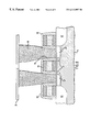
- FIG. 1 is a sectional view of a semiconductor wafer fragment at one processing step in accordance with the invention.
- FIG. 2 is a view of the FIG. 1 wafer taken at a step subsequent to that shown by FIG. 1 .
- FIG. 2 shows the formation of actual gate, and dummy gate (or poly runners over field oxide), structures at a predetermined height (H) and spacing (S).
- FIG. 2 also shows formation of a lightly doped drain LDD between such structures.
- FIG. 3 is a view of the FIG. 1 wafer taken at a step subsequent to that shown by FIG. 2, and shows self-aligned formation of source and drain regions.
- FIG. 4 is a view of the FIG. 1 wafer taken at a step subsequent to that shown by FIG. 3, and shows spacering of actual gate, and dummy gates (or poly runners over field oxide), and angled implant for punch through prevention.
- FIG. 4 also shows a gradation in the P-N junction region of the active area as a result of the shadow effects caused by the angled implant and the structures at distances H and S.
- FIG. 5 is a view of the FIG. 1 wafer taken at a step subsequent to that shown by FIG. 4, and shows one method of contact formation to source and drain regions.
- FIG. 6 is a view of the FIG. 1 wafer taken at a step subsequent to that shown by FIG. 4, and shows an alternative method of contact formation to source and drain regions.
- FIG. 7 is an alternative embodiment showing a view of the FIG. 1 wafer taken at a step subsequent to FIG. 1, and shows formation of a lightly doped drain and angled implant for punch through prevention, both prior to spacering of actual gate and dummy gates (or poly runners).
- FIG. 8 depicts examples of various circuits containing both low V t devices and high or normal V t devices according to the present invention.
- substrate herein shall be understood to mean one or more semiconductive layers or structures which include active or operable portions of semiconductor devices.
- a fabrication process for a low voltage semiconductor transistor device is described below. It is to be understood, however, that this process is only one example of many possible processes.
- the angled V t adjustment implant is shadowed out by a transistor gate and a dummy gate in the following process.
- a series of actual gates, interconnect structures and actual, or dummy, gates, poly runners or other structures could also be used.
- additional implant steps may be employed to optimize impurity profiles in particular regions, and the sequence of implant steps could be changed so long as the punch through prevention implant is carried out after one or more structures are deposited and subsequently patterned with sufficient height and sufficiently small spacing to shadow out the angled implant.
- a first pad oxide layer 11 is grown on lightly-doped P-type silicon substrate 12 .
- Silicon substrate 12 is isolated into active region 10 by field oxide regions 13 .
- LOCal Oxidation of Silicon (LOCOS), shallow trench isolation (STI) or other field isolation techniques known in the art are used to provide oxide regions 13 for patterning silicon substrate 12 into active region 10 .
- a silicon nitride layer (not shown) can be deposited on a silicon dioxide layer which is previously thermally grown on silicon substrate 12 . The silicon nitride layer is patterned such that the silicon nitride layer remains only on active region 10 .
- a silicon trench is then etched to a depth of typically 2-3 times the junction depth of the devices, i.e., about 0.20 to 0.40 micron.
- the silicon sidewalls and trench bottom are then oxidized to a thickness of about 100-200 angstroms to serve as a liner.
- a high conformal oxide deposition is performed to fill both the trench and the wide open field area.
- the oxide is subsequently planarized by chemical mechanical polishing (CMP) to the level of the nitride underneath, to expose the nitride.
- CMP chemical mechanical polishing
- the STI process is preferred in the method of the present invention due to the greater degree of flatness or planarity which it provides.
- gate structure 18 which includes polycrystalline silicon 14 , an overlying silicide layer 15 such as tungsten silicide or other highly conductive materials, and an insulating cap 16 , preferably SiO 2 or Si 3 N 4 , are formed using conventional semiconductor gate processing techniques.
- gate structure 18 is the actual transistor gate above active region 10 .
- Gate structures 26 above field oxide regions 13 are dummy gates or poly runners. Dummy gates 26 are preferably formed at the same time and using the same steps as used for formation of gate structure 18 .
- the height (H) of deposited polycrystalline silicon 14 , silicide 15 and cap 16 is the desired final height of gate structure 18 and dummy gate structures 26 for the semiconductor device.
- This height (H) is preferably greater than conventional gate structures so as to facilitate the shadow effects of the angled implant to adjust V t in subsequent steps.
- Patterned photoresist is used as an etch mask in forming gate structure 18 and dummy gates 26 . In FIG. 2, the patterned photoresist has been removed.
- a conventional self-aligning lightly doped (LDD) implant 20 is performed to form lightly doped regions 17 as shown.
- the LDD implant 20 is an N-type dopant.
- the LDD implant is a P-type dopant.
- the implant energy of the LDD implant 20 is sufficient to penetrate the exposed portion of active region 10 but not sufficient to penetrate active region 10 under gate structure 18 .
- gate structure 18 serves as an implant mask to block the LDD implant 20 .
- the implant energy of the LDD implant 20 controls the peak concentration depth.
- Lightly doped drain region 17 reduces the electric field of the semiconductor device by grading the doping level of active region 10 . This doping level gradation is discussed below in connection with FIG. 4 .
- a patterned photoresist may optionally be used to prevent self-aligning LDD implant 20 from penetrating other active regions which do not require the implant.
- the photoresist covered active regions include those used for semiconductor devices with a channel of a different conductivity type compared to that of the semiconductor device of gate structure 18 or to block certain species from being implanted into the memory array.
- the patterned photoresist is removed after performing LDD implant 20 .
- LDD implant 20 is followed by a chemical vapor deposition (CVD) of oxide or nitride to create a spacer oxide layer 19 having a thickness in the range of 200 to 2000 angstroms, depending upon device geometry.
- Spacer oxide layer 19 is then etched with an anisotropic etch, to form a set of sidewall spacers 19 for transistor gates 18 .
- Spacer oxide layer 19 coats the sides of transistor gate 18 , so that when the wafer is subsequently subjected to an N-type implant, N-type source/drain regions are created for N-channel devices, and these N-type source/drain regions are offset from the vertical boundaries of LDD implant regions 17 by the vertical segments of spacer oxide layer 19 on the edge of the N-channel transistor gates 18 .
- a high-dosage arsenic or phosphorus implant then creates self-aligned heavily doped N-type source/drain regions 23 for N-channel devices.
- the high-dosage implant is self-aligned to the edges of the N-channel transistor gate 18 .
- FIG. 3 depicts self-aligning implant 22 performed after formation of gate structure 18 and oxide spacer 19 .
- the self-alignment of implant 22 is particularly preferred for small geometry devices.
- Implant 22 introduces dopant into active region 10 to overlap LDD region 17 to form source and drain regions 23 .
- dopant 22 is a dopant having an N-type conductivity such as phosphorous, arsenic, or the like.
- Dopant 22 is, of course, of a different conductivity type than that of the substrate to form a semiconductor device with a channel of the different conductivity type.
- the implant energy of dopant 22 during implant 22 is sufficient to penetrate active region 10 in source and drain region 23 , i.e., the implant energy is preferably low to form shallow junctions.
- Gate structure 18 serves as an implant mask to block implant 22 .
- the implant energy of dopant 22 controls the depth of the peak concentration of implant 22 .
- An additional implant can be used to optimize the dopant profile of source and drain region 23 .
- a portion of source and drain region 23 will exist underneath a portion of spacer 19 , in that a portion of LDD region 17 exists underneath a portion of gate structure 18 since the LDD implant is performed prior to the formation of spacer 19 .
- a portion of LDD region 17 is converted into source and drain region 23 by implant 22 .
- LDD region 17 and source and drain region 23 are of the same conductivity type.
- spacer 19 is used to block implant 22 from completely overlapping LDD region 17 .
- the doping concentration of source and drain region 23 is higher than the doping concentration of LDD region 17 , and the doping concentration of LDD region 17 does not significantly affect the doping concentration of source and drain region 23 .
- Source and drain region 23 has a higher N-type doping concentration, and LDD region 17 has a lower N-type doping concentration.
- a portion of the original LDD region exists to provide a graded doping concentration to reduce the electric field in active region 10 to increase the breakdown voltage of the semiconductor device.
- the wafer is subjected to angled low-dosage boron implant 21 , using a mask which is usually the same mask as the N+ source/drain mask, to serve as an N-channel punch through voltage enhancement, creating punch through implant regions 24 that extend to the edges of transistor gate 18 and dummy gate 26 .
- Punch through prevention implant 21 introduces dopant into active region 10 , and may increase V t of small devices by as much as several hundred mVs.
- the implanted dopant 21 is a dopant having a P-type conductivity such as boron.
- Dopant 21 is of a different conductivity type to prevent punch through in a channel of the different conductivity type.
- a P-type dopant is implanted into an N-channel device to prevent punch through.
- an N-type dopant such as phosphorous, can be implanted into an N-channel device to adjust the threshold voltage in a negative direction.
- the threshold voltage adjustment implant is performed prior to formation of gate structure 18 and spacer 19 .
- the gate structure serves as a mask for the angled implant 21 , and the implant 22 (FIG. 3) which creates the source and drain regions.
- implant 21 is a different conductivity type than implant 22
- the implant dose of implant 22 is approximately 3 orders of magnitude higher than the implant dose of implant 21 . Therefore, although P-type punch through prevention implant 21 is implanted into N-type source and drain region 23 , the lower concentration of P-type dopant 21 does not significantly affect the higher concentration of N-type dopant 22 . A similar effect is observed if implant 21 uses an N-type dopant.
- Implant 21 is performed at a boron implant dose of approximately 2 ⁇ 10 11 to 8 ⁇ 10 13 atoms/cm 2 and an implant energy of approximately 10 to 100 keV, preferably about 40 to 60 keV.
- the method of the present invention uses an angled implant 21 in which the relatively tall (H) gate structures partially shadow out implant 21 .
- H relatively tall
- the implant angle ⁇ is between 5° and 45° as shown in FIG. 4, and the gate or other structures are sufficiently high so that the implant angle is preferably slightly greater than Arc tangent S/H, where S is the horizontal distance between gate structure 18 and dummy gates 26 (or other structures), only a thin layer of boron is created in region 24 below the source and drain regions.
- Implants 21 and 22 are subsequently annealed to activate implanted dopants 21 and 22 , respectively.
- the high temperature anneal or rapid thermal anneal is preferably of a short time duration to prevent dopant diffusion associated with long diffusion anneals and to eliminate problems associated with dopant diffusion.
- FIG. 5 conventional processing technology may be used to complete the circuitry.
- oxide isolation layer (not shown), which may be doped with phosphorus, boron or both.
- a photomask (not shown) has been used to define contacts 28 from metal layer 31 through oxide isolation layer through which connection to poly plug structures 27 and active area conductive regions below can be made.
- FIG. 5 shows buried digit line 29 as one preferred embodiment.
- FIG. 6 an alternative embodiment is shown which utilizes a self-aligned contact etch for tungsten metal contacts 30 .
- Various processing steps known in the art can be used to complete the circuitry.
- Additional variations of the present invention include interchanging the processing order of source and drain implant 22 and punch through prevention implant 21 .
- the implant 21 can be formed together with the LDD implant step before spacer formation.
- FIG. 7 illustrates process steps in this alternative embodiment.
- the semiconductor manufacturing process embodied in the present invention to produce MOS semiconductor transistor devices can also be used to produce MESFET, CMOS, and BiCMOS devices.
- V t devices may be made on a chip containing normal or high V t devices without the need for any additional masking step.
- the invention thus lends itself well to various applications in which low voltage devices are minority devices on a given chip. These applications, include, for example, NMOS pass transistor devices (FIG. 8 A), pre-charge circuits (FIG. 8B) and output drivers (FIG. 8 C).
- V TL represents a low threshold voltage device, which preferably has a low V t so as to maximize output level at VO, due to the V t drop.
- Voltage V 1 after a pass transistor is preferably high to have good drive on the device M 1 . The smaller the V t , the lower the drop.
- the node 1 voltage of the pre-charge circuit V PR is preferably high so that it can properly drive the subsequent driver. Accordingly, a V TL device is provided between V PR and node 1 .
- FIG. 8C shows another circuit in which the output is a V t drop away from the input voltage V cc . Given the disclosure and teachings of the present invention, these and various other circuits can now be conveniently made with both low V t and high V t devices without additional or complex processing steps.
- such structures are of sufficient height (H) and spacing (S) such that the implant angle is greater than or equal to arc tangent S/H.
- the structures may include, for example, an actual gate for one device and an adjacent actual gate of another device, or an actual gate for one device and an interconnect structure such as a poly runner for that same or another device.
Abstract
Description
Claims (31)
Priority Applications (4)
| Application Number | Priority Date | Filing Date | Title |
|---|---|---|---|
| US09/132,904 US6312997B1 (en) | 1998-08-12 | 1998-08-12 | Low voltage high performance semiconductor devices and methods |
| US09/903,623 US6492693B2 (en) | 1998-08-12 | 2001-07-13 | Low voltage high performance semiconductor devices and methods |
| US10/302,965 US6747326B2 (en) | 1998-08-12 | 2002-11-25 | Low voltage high performance semiconductor device having punch through prevention implants |
| US10/831,192 US6946353B2 (en) | 1998-08-12 | 2004-04-26 | Low voltage high performance semiconductor devices and methods |
Applications Claiming Priority (1)
| Application Number | Priority Date | Filing Date | Title |
|---|---|---|---|
| US09/132,904 US6312997B1 (en) | 1998-08-12 | 1998-08-12 | Low voltage high performance semiconductor devices and methods |
Related Child Applications (1)
| Application Number | Title | Priority Date | Filing Date |
|---|---|---|---|
| US09/903,623 Division US6492693B2 (en) | 1998-08-12 | 2001-07-13 | Low voltage high performance semiconductor devices and methods |
Publications (1)
| Publication Number | Publication Date |
|---|---|
| US6312997B1 true US6312997B1 (en) | 2001-11-06 |
Family
ID=22456106
Family Applications (4)
| Application Number | Title | Priority Date | Filing Date |
|---|---|---|---|
| US09/132,904 Expired - Fee Related US6312997B1 (en) | 1998-08-12 | 1998-08-12 | Low voltage high performance semiconductor devices and methods |
| US09/903,623 Expired - Lifetime US6492693B2 (en) | 1998-08-12 | 2001-07-13 | Low voltage high performance semiconductor devices and methods |
| US10/302,965 Expired - Lifetime US6747326B2 (en) | 1998-08-12 | 2002-11-25 | Low voltage high performance semiconductor device having punch through prevention implants |
| US10/831,192 Expired - Fee Related US6946353B2 (en) | 1998-08-12 | 2004-04-26 | Low voltage high performance semiconductor devices and methods |
Family Applications After (3)
| Application Number | Title | Priority Date | Filing Date |
|---|---|---|---|
| US09/903,623 Expired - Lifetime US6492693B2 (en) | 1998-08-12 | 2001-07-13 | Low voltage high performance semiconductor devices and methods |
| US10/302,965 Expired - Lifetime US6747326B2 (en) | 1998-08-12 | 2002-11-25 | Low voltage high performance semiconductor device having punch through prevention implants |
| US10/831,192 Expired - Fee Related US6946353B2 (en) | 1998-08-12 | 2004-04-26 | Low voltage high performance semiconductor devices and methods |
Country Status (1)
| Country | Link |
|---|---|
| US (4) | US6312997B1 (en) |
Cited By (10)
| Publication number | Priority date | Publication date | Assignee | Title |
|---|---|---|---|---|
| US20010012664A1 (en) * | 1999-09-01 | 2001-08-09 | Tran Luan C. | Semiconductor processing methods of forming transistors, semiconductor processing methods of forming dynamic random access memory circuitry, and related integrated circuitry |
| US20030036235A1 (en) * | 1999-09-01 | 2003-02-20 | Tran Luan C. | Semiconductor processing methods of forming integrated circuitry |
| US6541359B1 (en) * | 2000-01-31 | 2003-04-01 | Koninklijke Philips Electronics N.V. | Optimized gate implants for reducing dopant effects during gate etching |
| US6635522B2 (en) * | 1999-11-30 | 2003-10-21 | Samsung Electronics Co., Ltd. | Method of forming a MOS transistor in a semiconductor device and a MOS transistor fabricated thereby |
| US20030209758A1 (en) * | 2002-05-13 | 2003-11-13 | Ga Won Lee | Transistor of semiconductor device, and method for forming the same |
| US20060022279A1 (en) * | 2002-08-26 | 2006-02-02 | Tran Luan C | Semiconductor constructions |
| US7049185B2 (en) * | 1999-12-13 | 2006-05-23 | Nec Electronics Corporation | Semiconductor device having dummy gates and its manufacturing method |
| US20110127588A1 (en) * | 2009-12-01 | 2011-06-02 | International Business Machines Corporation | Enhancing mosfet performance by optimizing stress properties |
| CN106601620A (en) * | 2015-10-16 | 2017-04-26 | 中芯国际集成电路制造(上海)有限公司 | Semiconductor device, preparation method thereof and electronic device |
| US20180226477A1 (en) * | 2014-06-10 | 2018-08-09 | International Business Machines Corporation | Tunable breakdown voltage rf fet devices |
Families Citing this family (22)
| Publication number | Priority date | Publication date | Assignee | Title |
|---|---|---|---|---|
| JP3730947B2 (en) * | 2002-10-08 | 2006-01-05 | 松下電器産業株式会社 | Manufacturing method of semiconductor device |
| JP4085891B2 (en) * | 2003-05-30 | 2008-05-14 | ソニー株式会社 | Semiconductor device and manufacturing method thereof |
| US7499674B2 (en) * | 2003-09-12 | 2009-03-03 | Nokia Corporation | Method and system for repeat request in hybrid ultra wideband-bluetooth radio |
| US20050056881A1 (en) * | 2003-09-15 | 2005-03-17 | Yee-Chia Yeo | Dummy pattern for silicide gate electrode |
| DE102004002232B4 (en) * | 2004-01-15 | 2007-09-13 | OCé PRINTING SYSTEMS GMBH | Multifunction device for postprocessing a printed material web printed by an electrographic printing device |
| US7705405B2 (en) * | 2004-07-06 | 2010-04-27 | International Business Machines Corporation | Methods for the formation of fully silicided metal gates |
| US7462903B1 (en) * | 2005-09-14 | 2008-12-09 | Spansion Llc | Methods for fabricating semiconductor devices and contacts to semiconductor devices |
| EP1935026A1 (en) * | 2005-10-12 | 2008-06-25 | Acco | Insulated gate field-effet transistor having a dummy gate |
| KR20070055729A (en) * | 2005-11-28 | 2007-05-31 | 동부일렉트로닉스 주식회사 | Structure of semiconductor device having dummy gate and fabrication method thereof |
| FR2898729B1 (en) * | 2006-03-17 | 2008-08-01 | St Microelectronics | SEMICONDUCTOR DEVICE AND METHOD FOR IMPLANTING DOPANTS IN A CHANNEL |
| US7582520B2 (en) * | 2006-07-19 | 2009-09-01 | United Microelectronics Corp. | Method of fabricating complementary metal-oxide-semiconductor transistor and metal-oxide-semiconductor transistor |
| US7727838B2 (en) * | 2007-07-27 | 2010-06-01 | Texas Instruments Incorporated | Method to improve transistor Tox using high-angle implants with no additional masks |
| CN101211765B (en) * | 2007-12-21 | 2011-09-21 | 上海宏力半导体制造有限公司 | Shallow impurity drain domain logical operation method capable of diminishing ion implantation shadow effect |
| US7863645B2 (en) * | 2008-02-13 | 2011-01-04 | ACCO Semiconductor Inc. | High breakdown voltage double-gate semiconductor device |
| US9240402B2 (en) | 2008-02-13 | 2016-01-19 | Acco Semiconductor, Inc. | Electronic circuits including a MOSFET and a dual-gate JFET |
| US8928410B2 (en) | 2008-02-13 | 2015-01-06 | Acco Semiconductor, Inc. | Electronic circuits including a MOSFET and a dual-gate JFET |
| US7969243B2 (en) | 2009-04-22 | 2011-06-28 | Acco Semiconductor, Inc. | Electronic circuits including a MOSFET and a dual-gate JFET |
| US8532584B2 (en) | 2010-04-30 | 2013-09-10 | Acco Semiconductor, Inc. | RF switches |
| FR2970813B1 (en) * | 2011-01-24 | 2013-09-27 | Commissariat Energie Atomique | FIELD EFFECT DEVICE PROVIDED WITH A LOCALIZED DOPING DIFFUSION BARRIER ZONE AND METHOD OF REALIZING THE SAME |
| US8822278B2 (en) | 2012-03-29 | 2014-09-02 | International Business Machines Corporation | Asymmetric FET formed through use of variable pitch gate for use as logic device and test structure |
| CN103715133B (en) * | 2012-09-29 | 2016-01-06 | 中芯国际集成电路制造(上海)有限公司 | Mos transistor and forming method thereof |
| WO2019227359A1 (en) * | 2018-05-30 | 2019-12-05 | 深圳市柔宇科技有限公司 | Thin-film transistor and manufacturing method therefor, array substrate and display apparatus |
Citations (30)
| Publication number | Priority date | Publication date | Assignee | Title |
|---|---|---|---|---|
| US3912545A (en) | 1974-05-13 | 1975-10-14 | Motorola Inc | Process and product for making a single supply N-channel silicon gate device |
| US4232439A (en) * | 1976-11-30 | 1980-11-11 | Vlsi Technology Research Association | Masking technique usable in manufacturing semiconductor devices |
| US4418094A (en) | 1982-03-02 | 1983-11-29 | Texas Instruments Incorporated | Vertical-etch direct moat isolation process |
| US4839301A (en) | 1988-12-19 | 1989-06-13 | Micron Technology, Inc. | Blanket CMOS channel stop implant employing a combination of n-channel and p-channel punch-through implants |
| US4845047A (en) | 1987-06-25 | 1989-07-04 | Texas Instruments Incorporated | Threshold adjustment method for an IGFET |
| US5021353A (en) | 1990-02-26 | 1991-06-04 | Micron Technology, Inc. | Split-polysilicon CMOS process incorporating self-aligned silicidation of conductive regions |
| US5073509A (en) | 1989-12-11 | 1991-12-17 | Micron Technology, Inc. | Blanket CMOS channel-stop implant |
| US5087951A (en) | 1988-05-02 | 1992-02-11 | Micron Technology | Semiconductor memory device transistor and cell structure |
| JPH04274370A (en) * | 1991-03-01 | 1992-09-30 | Matsushita Electron Corp | Semiconductor device and manufacture thereof and semiconductor integrated circuit |
| JPH04329632A (en) * | 1991-04-30 | 1992-11-18 | Nec Corp | Manufacture of semiconductor device |
| US5252504A (en) | 1988-05-02 | 1993-10-12 | Micron Technology, Inc. | Reverse polysilicon CMOS fabrication |
| US5260593A (en) | 1991-12-10 | 1993-11-09 | Micron Technology, Inc. | Semiconductor floating gate device having improved channel-floating gate interaction |
| US5331191A (en) | 1989-03-20 | 1994-07-19 | Hitachi, Ltd. | Semiconductor integrated circuit device, process for fabricating the same, and apparatus for fabricating the same |
| US5355006A (en) * | 1991-09-09 | 1994-10-11 | Sharp Kabushiki Kaisha | Semiconductor memory device with source and drain limited to areas near the gate electrodes |
| US5355066A (en) * | 1989-10-20 | 1994-10-11 | Applied Materials, Inc. | Two-axis magnetically coupled robot |
| US5372957A (en) * | 1993-07-22 | 1994-12-13 | Taiwan Semiconductor Manufacturing Company | Multiple tilted angle ion implantation MOSFET method |
| US5413945A (en) * | 1994-08-12 | 1995-05-09 | United Micro Electronics Corporation | Blanket N-LDD implantation for sub-micron MOS device manufacturing |
| US5508541A (en) | 1992-09-22 | 1996-04-16 | Kabushiki Kaisha Toshiba | Random access memory device with trench-type one-transistor memory cell structure |
| US5572040A (en) | 1993-07-12 | 1996-11-05 | Peregrine Semiconductor Corporation | High-frequency wireless communication system on a single ultrathin silicon on sapphire chip |
| US5612630A (en) | 1995-12-19 | 1997-03-18 | Micron Technology, Inc. | Asynchronous self-adjusting input circuit |
| US5624863A (en) | 1995-07-17 | 1997-04-29 | Micron Technology, Inc. | Semiconductor processing method of forming complementary N-type doped and P-type doped active regions within a semiconductor substrate |
| US5648672A (en) | 1995-05-24 | 1997-07-15 | Sharp Kabushiki Kaisha | Semiconductor device with outer diffusion layer |
| US5650350A (en) | 1995-08-11 | 1997-07-22 | Micron Technology, Inc. | Semiconductor processing method of forming a static random access memory cell and static random access memory cell |
| US5656836A (en) | 1990-02-09 | 1997-08-12 | Hitachi, Ltd. | Semiconductor integrated circuit device and process for fabricating the same |
| US5661045A (en) | 1993-05-24 | 1997-08-26 | Micron Technology, Inc. | Method for forming and tailoring the electrical characteristics of semiconductor devices |
| US5670392A (en) * | 1994-07-04 | 1997-09-23 | Sgs-Thomson Microelectronics S.R.L. | Process for manufacturing high-density MOS-technology power devices |
| JPH09289315A (en) * | 1996-04-22 | 1997-11-04 | Sony Corp | Semiconductor device manufacturing method |
| US5693505A (en) | 1993-12-24 | 1997-12-02 | Nec Corporation | Method of fabricating a semiconductor device |
| US5736416A (en) * | 1994-12-28 | 1998-04-07 | Nec Corporation | Fabrication process for MOSFET using oblique rotation ion implantation |
| US5834347A (en) * | 1994-04-28 | 1998-11-10 | Nippondenso Co., Ltd. | MIS type semiconductor device and method for manufacturing same |
Family Cites Families (14)
| Publication number | Priority date | Publication date | Assignee | Title |
|---|---|---|---|---|
| GB1173150A (en) * | 1966-12-13 | 1969-12-03 | Associated Semiconductor Mft | Improvements in Insulated Gate Field Effect Transistors |
| JPS63299251A (en) * | 1987-05-29 | 1988-12-06 | Toshiba Corp | Manufacture of semiconductor device |
| US5132753A (en) * | 1990-03-23 | 1992-07-21 | Siliconix Incorporated | Optimization of BV and RDS-on by graded doping in LDD and other high voltage ICs |
| US5275965A (en) * | 1992-11-25 | 1994-01-04 | Micron Semiconductor, Inc. | Trench isolation using gated sidewalls |
| US5349225A (en) * | 1993-04-12 | 1994-09-20 | Texas Instruments Incorporated | Field effect transistor with a lightly doped drain |
| JPH07201885A (en) * | 1993-12-28 | 1995-08-04 | Fujitsu Ltd | Manufacture of semiconductor device |
| US5448090A (en) * | 1994-08-03 | 1995-09-05 | International Business Machines Corporation | Structure for reducing parasitic leakage in a memory array with merged isolation and node trench construction |
| US6346439B1 (en) * | 1996-07-09 | 2002-02-12 | Micron Technology, Inc. | Semiconductor transistor devices and methods for forming semiconductor transistor devices |
| US5895243A (en) * | 1996-04-16 | 1999-04-20 | Micron Technology, Inc. | Semiconductor processing method of providing electrical isolation between adjacent semiconductor diffusion regions of different field effect transistors and integrated circuitry having adjacent electrically isolated field effect transistors |
| US5858831A (en) * | 1998-02-27 | 1999-01-12 | Vanguard International Semiconductor Corporation | Process for fabricating a high performance logic and embedded dram devices on a single semiconductor chip |
| US6594193B2 (en) * | 2000-06-22 | 2003-07-15 | Progressent Technologies, Inc. | Charge pump for negative differential resistance transistor |
| US6545904B2 (en) * | 2001-03-16 | 2003-04-08 | Micron Technology, Inc. | 6f2 dram array, a dram array formed on a semiconductive substrate, a method of forming memory cells in a 6f2 dram array and a method of isolating a single row of memory cells in a 6f2 dram array |
| US6743684B2 (en) * | 2002-10-11 | 2004-06-01 | Texas Instruments Incorporated | Method to produce localized halo for MOS transistor |
| US6723623B1 (en) * | 2002-12-20 | 2004-04-20 | Micron Technology, Inc. | Methods of forming implant regions relative to transistor gates |
-
1998
- 1998-08-12 US US09/132,904 patent/US6312997B1/en not_active Expired - Fee Related
-
2001
- 2001-07-13 US US09/903,623 patent/US6492693B2/en not_active Expired - Lifetime
-
2002
- 2002-11-25 US US10/302,965 patent/US6747326B2/en not_active Expired - Lifetime
-
2004
- 2004-04-26 US US10/831,192 patent/US6946353B2/en not_active Expired - Fee Related
Patent Citations (30)
| Publication number | Priority date | Publication date | Assignee | Title |
|---|---|---|---|---|
| US3912545A (en) | 1974-05-13 | 1975-10-14 | Motorola Inc | Process and product for making a single supply N-channel silicon gate device |
| US4232439A (en) * | 1976-11-30 | 1980-11-11 | Vlsi Technology Research Association | Masking technique usable in manufacturing semiconductor devices |
| US4418094A (en) | 1982-03-02 | 1983-11-29 | Texas Instruments Incorporated | Vertical-etch direct moat isolation process |
| US4845047A (en) | 1987-06-25 | 1989-07-04 | Texas Instruments Incorporated | Threshold adjustment method for an IGFET |
| US5252504A (en) | 1988-05-02 | 1993-10-12 | Micron Technology, Inc. | Reverse polysilicon CMOS fabrication |
| US5087951A (en) | 1988-05-02 | 1992-02-11 | Micron Technology | Semiconductor memory device transistor and cell structure |
| US4839301A (en) | 1988-12-19 | 1989-06-13 | Micron Technology, Inc. | Blanket CMOS channel stop implant employing a combination of n-channel and p-channel punch-through implants |
| US5331191A (en) | 1989-03-20 | 1994-07-19 | Hitachi, Ltd. | Semiconductor integrated circuit device, process for fabricating the same, and apparatus for fabricating the same |
| US5355066A (en) * | 1989-10-20 | 1994-10-11 | Applied Materials, Inc. | Two-axis magnetically coupled robot |
| US5073509A (en) | 1989-12-11 | 1991-12-17 | Micron Technology, Inc. | Blanket CMOS channel-stop implant |
| US5656836A (en) | 1990-02-09 | 1997-08-12 | Hitachi, Ltd. | Semiconductor integrated circuit device and process for fabricating the same |
| US5021353A (en) | 1990-02-26 | 1991-06-04 | Micron Technology, Inc. | Split-polysilicon CMOS process incorporating self-aligned silicidation of conductive regions |
| JPH04274370A (en) * | 1991-03-01 | 1992-09-30 | Matsushita Electron Corp | Semiconductor device and manufacture thereof and semiconductor integrated circuit |
| JPH04329632A (en) * | 1991-04-30 | 1992-11-18 | Nec Corp | Manufacture of semiconductor device |
| US5355006A (en) * | 1991-09-09 | 1994-10-11 | Sharp Kabushiki Kaisha | Semiconductor memory device with source and drain limited to areas near the gate electrodes |
| US5260593A (en) | 1991-12-10 | 1993-11-09 | Micron Technology, Inc. | Semiconductor floating gate device having improved channel-floating gate interaction |
| US5508541A (en) | 1992-09-22 | 1996-04-16 | Kabushiki Kaisha Toshiba | Random access memory device with trench-type one-transistor memory cell structure |
| US5661045A (en) | 1993-05-24 | 1997-08-26 | Micron Technology, Inc. | Method for forming and tailoring the electrical characteristics of semiconductor devices |
| US5572040A (en) | 1993-07-12 | 1996-11-05 | Peregrine Semiconductor Corporation | High-frequency wireless communication system on a single ultrathin silicon on sapphire chip |
| US5372957A (en) * | 1993-07-22 | 1994-12-13 | Taiwan Semiconductor Manufacturing Company | Multiple tilted angle ion implantation MOSFET method |
| US5693505A (en) | 1993-12-24 | 1997-12-02 | Nec Corporation | Method of fabricating a semiconductor device |
| US5834347A (en) * | 1994-04-28 | 1998-11-10 | Nippondenso Co., Ltd. | MIS type semiconductor device and method for manufacturing same |
| US5670392A (en) * | 1994-07-04 | 1997-09-23 | Sgs-Thomson Microelectronics S.R.L. | Process for manufacturing high-density MOS-technology power devices |
| US5413945A (en) * | 1994-08-12 | 1995-05-09 | United Micro Electronics Corporation | Blanket N-LDD implantation for sub-micron MOS device manufacturing |
| US5736416A (en) * | 1994-12-28 | 1998-04-07 | Nec Corporation | Fabrication process for MOSFET using oblique rotation ion implantation |
| US5648672A (en) | 1995-05-24 | 1997-07-15 | Sharp Kabushiki Kaisha | Semiconductor device with outer diffusion layer |
| US5624863A (en) | 1995-07-17 | 1997-04-29 | Micron Technology, Inc. | Semiconductor processing method of forming complementary N-type doped and P-type doped active regions within a semiconductor substrate |
| US5650350A (en) | 1995-08-11 | 1997-07-22 | Micron Technology, Inc. | Semiconductor processing method of forming a static random access memory cell and static random access memory cell |
| US5612630A (en) | 1995-12-19 | 1997-03-18 | Micron Technology, Inc. | Asynchronous self-adjusting input circuit |
| JPH09289315A (en) * | 1996-04-22 | 1997-11-04 | Sony Corp | Semiconductor device manufacturing method |
Cited By (40)
| Publication number | Priority date | Publication date | Assignee | Title |
|---|---|---|---|---|
| US7057257B2 (en) * | 1999-09-01 | 2006-06-06 | Micron Technology, Inc. | Semiconductor processing methods of forming transistors, semiconductor processing methods of forming dynamic random access memory circuitry, and related integrated circuitry |
| US7341901B2 (en) * | 1999-09-01 | 2008-03-11 | Micron Technology, Inc. | Semiconductor processing methods of forming integrated circuitry |
| US20030020106A1 (en) * | 1999-09-01 | 2003-01-30 | Luan C. Tran | Semiconductor processing methods of forming transistors, semiconductor processing methods of forming dynamic random access memory circuitry, and related integrated circuitry |
| US20030036235A1 (en) * | 1999-09-01 | 2003-02-20 | Tran Luan C. | Semiconductor processing methods of forming integrated circuitry |
| US20020195670A1 (en) * | 1999-09-01 | 2002-12-26 | Tran Luan C. | Semiconductor processing methods of forming transistors, semiconductor processing methods of forming dynamic random access memory circuitry, and related integrated circuitry |
| US6579751B2 (en) * | 1999-09-01 | 2003-06-17 | Micron Technology, Inc. | Semiconductor processing methods of forming integrated circuitry |
| US7045405B2 (en) | 1999-09-01 | 2006-05-16 | Micron Technology, Inc. | Semiconductor processing methods of forming integrated circuitry |
| US7294903B2 (en) | 1999-09-01 | 2007-11-13 | Micron Technology, Inc. | Transistor assemblies |
| US7291880B2 (en) | 1999-09-01 | 2007-11-06 | Micron Technology, Inc. | Transistor assembly |
| US20040106253A1 (en) * | 1999-09-01 | 2004-06-03 | Tran Luan C. | Semiconductor processing methods of forming integrated circuitry |
| US20040209421A1 (en) * | 1999-09-01 | 2004-10-21 | Tran Luan C. | Semiconductor processing methods of forming integrated circuitry |
| US20050029599A1 (en) * | 1999-09-01 | 2005-02-10 | Tran Luan C. | Semiconductor processing methods of forming transistors, semiconductor processing methods of forming dynamic random access memory circuitry, and related integrated circuitry |
| US20050042810A1 (en) * | 1999-09-01 | 2005-02-24 | Tran Luan C. | Semiconductor processing methods of forming integrated circuitry |
| US6875646B2 (en) * | 1999-09-01 | 2005-04-05 | Micron Technology, Inc. | Semiconductor processing methods of forming integrated circuitry |
| US6914287B2 (en) * | 1999-09-01 | 2005-07-05 | Micron Technology, Inc | Semiconductor processing methods of forming transistors, semiconductor processing methods of forming dynamic random access memory circuitry, and related integrated circuitry |
| US20050287733A1 (en) * | 1999-09-01 | 2005-12-29 | Tran Luan C | Semiconductor processing methods of forming transistors, semiconductor processing methods of forming dynamic random access memory circuitry, and related integrated circuitry |
| US20060008977A1 (en) * | 1999-09-01 | 2006-01-12 | Tran Luan C | Semiconductor processing methods of forming transistors, semiconductor processing methods of forming dynamic random access memory circuitry, and related integrated circuitry |
| US20010012664A1 (en) * | 1999-09-01 | 2001-08-09 | Tran Luan C. | Semiconductor processing methods of forming transistors, semiconductor processing methods of forming dynamic random access memory circuitry, and related integrated circuitry |
| US20030153138A1 (en) * | 1999-09-01 | 2003-08-14 | Tran Luan C. | Semiconductor processing methods of forming integrated circuitry |
| US7253047B2 (en) | 1999-09-01 | 2007-08-07 | Micron Technology, Inc. | Semiconductor processing methods of forming transistors, semiconductor processing methods of forming dynamic random access memory circuitry, and related integrated circuitry |
| US7176093B2 (en) | 1999-09-01 | 2007-02-13 | Micron Technology, Inc. | Semiconductor processing methods of forming integrated circuitry |
| US7135363B2 (en) | 1999-09-01 | 2006-11-14 | Micron Technology, Inc. | Semiconductor processing methods of forming integrated circuitry |
| US20060211207A1 (en) * | 1999-09-01 | 2006-09-21 | Tran Luan C | Semiconductor processing methods of forming integrated circuitry |
| US6635522B2 (en) * | 1999-11-30 | 2003-10-21 | Samsung Electronics Co., Ltd. | Method of forming a MOS transistor in a semiconductor device and a MOS transistor fabricated thereby |
| US7049185B2 (en) * | 1999-12-13 | 2006-05-23 | Nec Electronics Corporation | Semiconductor device having dummy gates and its manufacturing method |
| US6541359B1 (en) * | 2000-01-31 | 2003-04-01 | Koninklijke Philips Electronics N.V. | Optimized gate implants for reducing dopant effects during gate etching |
| US20030209758A1 (en) * | 2002-05-13 | 2003-11-13 | Ga Won Lee | Transistor of semiconductor device, and method for forming the same |
| US20060022279A1 (en) * | 2002-08-26 | 2006-02-02 | Tran Luan C | Semiconductor constructions |
| US20060121712A1 (en) * | 2002-08-26 | 2006-06-08 | Micron Technology, Inc. | Semiconductor constructions and methods of forming semiconductor constructions |
| US20110127588A1 (en) * | 2009-12-01 | 2011-06-02 | International Business Machines Corporation | Enhancing mosfet performance by optimizing stress properties |
| US8318570B2 (en) * | 2009-12-01 | 2012-11-27 | International Business Machines Corporation | Enhancing MOSFET performance by optimizing stress properties |
| US20180226477A1 (en) * | 2014-06-10 | 2018-08-09 | International Business Machines Corporation | Tunable breakdown voltage rf fet devices |
| US10804364B2 (en) | 2014-06-10 | 2020-10-13 | International Business Machines Corporation | Tunable breakdown voltage RF FET devices |
| US10109716B2 (en) | 2014-06-10 | 2018-10-23 | International Business Machines Corporation | Turnable breakdown voltage RF FET devices |
| US10629692B2 (en) | 2014-06-10 | 2020-04-21 | International Business Machines Corporation | Tunable breakdown voltage RF FET devices |
| US10680074B2 (en) * | 2014-06-10 | 2020-06-09 | International Business Machines Corporation | Tunable breakdown voltage RF FET devices |
| US10770557B2 (en) | 2014-06-10 | 2020-09-08 | International Business Machines Corporation | Tunable breakdown voltage RF FET devices |
| US10790369B2 (en) | 2014-06-10 | 2020-09-29 | International Business Machines Corporation | Tunable breakdown voltage RF FET devices |
| CN106601620B (en) * | 2015-10-16 | 2019-09-27 | 中芯国际集成电路制造(上海)有限公司 | A kind of semiconductor devices and preparation method thereof, electronic device |
| CN106601620A (en) * | 2015-10-16 | 2017-04-26 | 中芯国际集成电路制造(上海)有限公司 | Semiconductor device, preparation method thereof and electronic device |
Also Published As
| Publication number | Publication date |
|---|---|
| US6747326B2 (en) | 2004-06-08 |
| US20030073269A1 (en) | 2003-04-17 |
| US6946353B2 (en) | 2005-09-20 |
| US20010039096A1 (en) | 2001-11-08 |
| US6492693B2 (en) | 2002-12-10 |
| US20040198004A1 (en) | 2004-10-07 |
Similar Documents
| Publication | Publication Date | Title |
|---|---|---|
| US6312997B1 (en) | Low voltage high performance semiconductor devices and methods | |
| US5773358A (en) | Method of forming a field effect transistor and method of forming CMOS integrated circuitry | |
| EP0074215B1 (en) | Cmos devices with self-aligned channel stops | |
| US5770490A (en) | Method for producing dual work function CMOS device | |
| US5424572A (en) | Spacer formation in a semiconductor structure | |
| US6028339A (en) | Dual work function CMOS device | |
| US7064399B2 (en) | Advanced CMOS using super steep retrograde wells | |
| US6759288B2 (en) | Double LDD devices for improved DRAM refresh | |
| US6686233B2 (en) | Integration of high voltage self-aligned MOS components | |
| US5897363A (en) | Shallow junction formation using multiple implant sources | |
| US5489546A (en) | Method of forming CMOS devices using independent thickness spacers in a split-polysilicon DRAM process | |
| US5682051A (en) | CMOS integrated circuit with reduced susceptibility to PMOS punchthrough | |
| US5618688A (en) | Method of forming a monolithic semiconductor integrated circuit having an N-channel JFET | |
| US6630377B1 (en) | Method for making high-gain vertical bipolar junction transistor structures compatible with CMOS process | |
| US6759717B2 (en) | CMOS integrated circuit device with LDD n-channel transistor and non-LDD p-channel transistor | |
| US5439831A (en) | Low junction leakage MOSFETs | |
| US6329271B1 (en) | Self-aligned channel implantation | |
| KR19990045046A (en) | Method of manufacturing BiCMOS semiconductor device | |
| US20060134874A1 (en) | Manufacture method of MOS semiconductor device having extension and pocket | |
| US20040041170A1 (en) | Low dose super deep source/drain implant | |
| US5898189A (en) | Integrated circuit including an oxide-isolated localized substrate and a standard silicon substrate and fabrication method | |
| US5399509A (en) | Method of manufacturing a bipolar transistor | |
| US6251744B1 (en) | Implant method to improve characteristics of high voltage isolation and high voltage breakdown | |
| US6218253B1 (en) | Method of manufacturing a bipolar transistor by using only two mask layers | |
| US6093595A (en) | Method of forming source and drain regions in complementary MOS transistors |
Legal Events
| Date | Code | Title | Description |
|---|---|---|---|
| AS | Assignment |
Owner name: MICRON TECHNOLOGY, INC., IDAHO Free format text: ASSIGNMENT OF ASSIGNORS INTEREST;ASSIGNOR:TRAN, LUAN C.;REEL/FRAME:009397/0400 Effective date: 19980804 |
|
| FPAY | Fee payment |
Year of fee payment: 4 |
|
| FEPP | Fee payment procedure |
Free format text: PAYER NUMBER DE-ASSIGNED (ORIGINAL EVENT CODE: RMPN); ENTITY STATUS OF PATENT OWNER: LARGE ENTITY Free format text: PAYOR NUMBER ASSIGNED (ORIGINAL EVENT CODE: ASPN); ENTITY STATUS OF PATENT OWNER: LARGE ENTITY |
|
| FPAY | Fee payment |
Year of fee payment: 8 |
|
| REMI | Maintenance fee reminder mailed | ||
| LAPS | Lapse for failure to pay maintenance fees | ||
| STCH | Information on status: patent discontinuation |
Free format text: PATENT EXPIRED DUE TO NONPAYMENT OF MAINTENANCE FEES UNDER 37 CFR 1.362 |
|
| FP | Lapsed due to failure to pay maintenance fee |
Effective date: 20131106 |