US6313672B1 - Over-voltage tolerant integrated circuit I/O buffer - Google Patents
Over-voltage tolerant integrated circuit I/O buffer Download PDFInfo
- Publication number
- US6313672B1 US6313672B1 US09/464,374 US46437499A US6313672B1 US 6313672 B1 US6313672 B1 US 6313672B1 US 46437499 A US46437499 A US 46437499A US 6313672 B1 US6313672 B1 US 6313672B1
- Authority
- US
- United States
- Prior art keywords
- circuit
- coupled
- transistor
- driver
- node
- Prior art date
- Legal status (The legal status is an assumption and is not a legal conclusion. Google has not performed a legal analysis and makes no representation as to the accuracy of the status listed.)
- Expired - Lifetime
Links
Images


Classifications
-
- H—ELECTRICITY
- H03—ELECTRONIC CIRCUITRY
- H03K—PULSE TECHNIQUE
- H03K19/00—Logic circuits, i.e. having at least two inputs acting on one output; Inverting circuits
- H03K19/003—Modifications for increasing the reliability for protection
- H03K19/00315—Modifications for increasing the reliability for protection in field-effect transistor circuits
Definitions
- the present invention relates to the field of integrated circuit products, and more specifically to a buffer circuit that is tolerant to over-voltage.
- the invention also relates to a method for protecting buffer circuits from over-voltage.
- gate-oxides in 0.35 ⁇ m technology can withstand a maximum of 3.6 V Specifically, the potential difference between gate-to-source, gate-to-drain, and gate-to-substrate should not exceed 3.6 V If such potential differences exceed 3.6 V, electrical problems, such as current leakage, can occur.
- a typical buffer circuit designed with CMOS digital integrated technology has driver PMOS transistors coupled in series between a supply-voltage VDD and an input/output node. Over-voltage can occur when a voltage at its input/output (I/O) node is higher than the I/O buffer supply-voltage VDD.
- a driver PMOS transistor can turn on if the source-to-gate voltage is greater than the PMOS threshold voltage. Also, when a 5 V input voltage appears at the I/O node, a P+/N-well diode from the I/O node to an N-well underneath the PMOS transistors turns on. As a result, the diode is forward biased and current leaks from the I/O node to the N-well.
- Such a circuit and method should thus prevent problems such as high leakage and gate-oxide damage.
- such a circuit and method should be cost effective and require little space.
- the present invention achieves these benefits in the context of known integrated circuit technology and known techniques in the art.
- the present invention provides a buffer circuit that can tolerate over-voltage, and a method for protecting buffer circuits from over-voltage.
- the buffer circuit can operate at lower voltages (e.g., 3.3 V) and interface with other circuits that operate at higher voltages (e.g., 5 V) at an interface node.
- the buffer circuit has a driver PMOS transistor, and a pre-driver circuit having a pull-up circuit coupled to the interface node via a PMOS switch transistor and a first PMOS pass transistor.
- the pre-driver biasing circuit is configured to decouple the pull-up circuit from the interface node when an input voltage at the interface node exceeds the VDD voltage by a PMOS threshold voltage.
- the buffer circuit has a first biasing transistor that ties an N-well of the integrated circuit to the VDD voltage source when a control node of a PMOS driver transistor is in a first logic state, and a second biasing transistor that ties the N-well to the VDD voltage source when the control node of the PMOS driver transistor is in a second logic state.
- the buffer circuit has a third biasing transistor that ties the N-well to the interface node when the input voltage at the interface node exceeds the VDD voltage by a PMOS threshold voltage.
- the buffer circuit also has a second pre-driver circuit and a second driver circuit.
- the first and second pre-driver circuits are configured to provide control signals to a first driver circuit and a second driver circuit, respectively.
- the pre-driver biasing circuit further includes a second PMOS pass transistor connected between the control node of the PMOS switch transistor and the control node of the PMOS driver transistor.
- the pre-driver biasing circuit further includes a third pass transistor coupled to the control node of the PMOS switch transistor, a control node of the third pass transistor being coupled to the VDD voltage source; and a first pre-driver biasing transistor coupled between the third pass transistor and a VSS voltage source, a control node of the first pre-driver biasing transistor being configured to receive an enable signal; and a second pre-driver biasing transistor coupled in parallel to the first pre-driver biasing transistor, a control node of the second pre-driver biasing transistor being configured to receive a second input signal.
- the present invention is a buffer circuit including a first feedback circuit and a second feedback circuit cross-coupled between the first and second pre-driver circuits.
- the first feedback circuit can include an NMOS transistor having a drain node coupled to a drain of the switch transistor, and a control node coupled to the VDD voltage source; an inverter having an input coupled to a source node of the NMOS transistor; and a PMOS transistor having a source node coupled to the VDD voltage source, a drain node coupled to the input of the inverter, and a control node coupled to an output of the inverter; wherein the output of the inverter is coupled to the second pre-driver circuit.
- One advantage of the present invention is that it when a high-voltage is applied to the I/O node, leakage current from I/O node to VDD is minimized.
- Another advantage of this design is that only one big driver PMOS is used. This saves about 4 times the area compared to that when using the alternative approach for high-voltage protection, that is, when two PMOS transistors are used in series.
- Another advantage of this design is that the new buffer circuit requires only a single gate-oxide thickness. This results in a significant reduction in fabrication costs and a significant increase in fabrication yield.
- the present invention accomplishes the above benefits and purposes in an inexpensive, uncomplicated, durable, versatile, and reliable circuit and method, inexpensive to manufacture, and readily suited to the widest possible utilization.
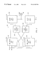
- FIG. 1 is a block diagram of an over-voltage tolerant integrated circuit buffer showing an input stage and an output stage;
- FIG. 2 is a block diagram of the output stage of the over-voltage tolerant integrated circuit buffer of FIG. 1;
- FIG. 3 is a schematic diagram of prior-art including an output stage of an integrated circuit buffer
- FIG. 4 is a detailed schematic diagram of an embodiment of the output stage of the over-voltage tolerant integrated circuit buffer of FIG. 1, including driver, pre-driver, and feedback circuits;
- FIG. 5 is a schematic diagram of an embodiment of the driver circuits of the output circuit of FIG. 4.
- FIG. 6 is a schematic diagram of an embodiment of the pre-driver PMOS circuit of FIG. 4 .
- FIG. 1 is a block diagram of an over-voltage tolerant integrated circuit buffer 100 showing an input stage 125 and an output stage 150 .
- FIG. 2 is a block diagram of the output stage 150 , or buffer circuit 150 , of the over-voltage tolerant integrated circuit buffer of FIG. 1 .
- the embodiment shown in FIG. 2 includes a driver PMOS circuit 210 and a driver NMOS circuit 220 operatively coupled to an I/O node 230 to source current to a load (not shown) via I/O node 230 , and to sink current from the load, respectively.
- Driver PMOS circuit 210 couples to a supply voltage, or VDD
- driver NMOS circuit 220 couples to a ground voltage, or VSS.
- VDD can be designed to be 2 V, 3 V, 4 V, or other voltages. In this specific embodiment, VDD is 3.3 V.
- VSS can be designed to be ⁇ 0.5 V, 0 V, 0.5 V, or other voltages. In this specific embodiment, VSS is 0 V.
- Driver PMOS circuit 210 operatively couples to a pre-driver PMOS circuit 260
- Driver NMOS circuit 220 operatively couples to a pre-driver NMOS circuit 270
- Both pre-driver PMOS circuit 260 and pre-driver NMOS circuit 270 couple to VDD and VSS. Also, both pre-driver circuits are configured to receive an input signal IN and an output enable signal OE.
- Pre-driver PMOS circuit 260 and pre-driver NMOS circuit 270 provide control signals to driver PMOS circuit 210 and driver NMOS circuit 220 , respectively.
- Driver PMOS circuit 210 also operatively couples to pre-driver NMOS circuit 270 via a PMOS feedback circuit 280 .
- driver NMOS circuit 270 operatively couples to pre-driver PMOS circuit 260 via an NMOS feedback circuit 290 .
- the feedback circuits ensure that both driver circuits are not conducting simultaneously. Simultaneous conduction of the driver circuits is undesirable, because it increases power dissipation in the circuit.
- buffer circuit 150 is described in two modes, input mode (or tri-state mode) and output mode (or normal mode), in this order.
- buffer circuit 150 receives an output enable signal OE that is at a logic low state.
- Driver circuits 210 and 220 are configured to turn off, or go into tri-state mode, when output enable signal OE is low. Accordingly, an input signal can pass through the buffer via I/O node 230 .
- a biasing circuit (not shown), integral to buffer circuit 150 , regulates the voltage potential-differences between the gates of buffer circuit 150 and corresponding sources, drains, and substrates (not shown).
- the biasing circuit maintains such voltage potential-differences to tolerable levels, and particularly, when a buffer circuit 150 is in input mode and a destructively high input voltage exists at I/O node 230 .
- a voltage can be 5 V or more.
- the biasing circuit (not shown) protects buffer circuit 150 from such high-voltages.
- the pre-driver circuits 260 and 270 receive an output enable signal OE that is at a logic high state.
- the driver circuits are configured so that they can turn on when output enable signal OE is high. Accordingly, an output signal can pass through the buffer via the driver circuits.
- FIG. 3 is a schematic diagram of prior-art including an output stage of an integrated circuit buffer. This output stage is not over-voltage tolerant.
- FIG. 4 is a detailed schematic diagram of an embodiment of the new invention of output stage 150 , or buffer circuit 150 , of the over-voltage tolerant integrated circuit buffer of FIG. 1 .
- Buffer circuit 150 includes several sub-circuits, each of which is described in detail in separate sections below.
- Buffer circuit 150 includes driver PMOS circuit 210 and a driver NMOS circuit 220 .
- Driver PMOS circuit 210 is first described.
- FIG. 5 is a schematic diagram of an embodiment of the driver circuits of buffer circuit 150 .
- Driver PMOS circuit 210 includes a pull-up circuit which, in this specific embodiment, is a driver PMOS transistor M 1 .
- Transistor M 1 couples between VDD and I/O node 230 to provide a source current to a load (not shown).
- the control input, or gate, of transistor M 1 couples to a pre-driver PMOS signal node 510 to receive a control signal from pre-driver PMOS circuit 260 (FIG. 3 ).
- Driver PMOS circuit 210 also includes a driver biasing circuit.
- the driver biasing circuit includes a plurality of transistors coupled to an N-well NW.
- the transistors of the driver biasing circuit are shown integrated into driver PMOS circuit 210 .
- four PMOS transistors M 2 , M 3 , M 4 and M 5 constitute the driver biasing circuit.
- PMOS pass transistor M 2 couples between the gate of transistor M 1 and I/O node 130 to tie the gate of transistor M 1 to the I/O node 130 during high-voltage conditions.
- the control input of the PMOS pass transistor M 2 couples to VDD.
- a PMOS pass transistor M 3 couples between N-well NW and I/O node 130 to tie N-well NW to I/O node 130 during high-voltage conditions.
- the control input of PMOS transistor M 3 is tied to VDD.
- Transistors M 4 and M 5 couple in parallel between VDD and N-well NW to tie N-well NW to VDD.
- the control input of transistor M 4 couples to I/O node 130
- the control input of transistor M 5 couples to the control input of transistor M 1 .
- the driver PMOS circuit 210 is described in two modes, input mode (or tri-state mode) and output mode (or normal mode), in this order.
- driver PMOS 210 circuit In input mode, driver PMOS 210 circuit is kept off by biasing the gate of transistor M 1 to a logic high.
- a P+/N-well diode D 1 (shown in dotted lines) is kept off by biasing N-well NW of driver PMOS circuit 210 to its highest potential.
- Diode D 1 is built into PMOS transistors M 1 , M 2 , and M 3 .
- the driver PMOS circuit regulates the voltage potential-differences between its gates to corresponding sources, drains, and substrates. Conditions are characterized as “high-voltage” conditions when the I/O node 130 is subjected to a high-voltage input such as 5 V or some other predetermined level above VDD.
- transistors M 2 and M 3 bias the gate of driver PMOS transistor M 1 and the N-well NW, respectively, to the high-voltage at I/O node 130 when the voltage at I/O node 130 is higher than VDD.
- transistor M 2 turns-on when the I/O node-to-gate voltage of M 2 exceeds its threshold voltage. (Under otherwise normal conditions, transistor M 2 is off because its gate is biased to VDD.)
- the gate of transistor M 1 is tied to the high-voltage of I/O node 130 .
- transistor M 1 Since the gate of transistor M 1 follows the high-voltage at I/O node 130 , the high-voltage at I/O node 130 propagates to NMOS and PMOS feedback circuits 280 and 290 (FIG. 2 ). The significance of this propagation is explained later.
- transistor M 3 turns-on when the I/O node-to-gate voltage of M 3 exceeds its threshold voltage. As a result, N-well NW is also tied to the high-voltage of the I/O node 130 .
- transistors M 4 and M 5 bias N-well NW to VDD. This results in minimal swing below VDD thus reducing the possibility of latch-up in this region.
- transistor M 4 or transistor M 5 is on including during output transitions (from logic high to low and vice versa).
- I/O node 130 When I/O node 130 is low, transistor M 4 is on. Conversely, and when I/O node 130 is high, due to transistor M 1 being on, transistor M 5 is on. (The state of transistor M 5 follows that of transistor M 1 because their gates coupled together).
- Transistors M 4 and M 5 are configured to overlap in conduction to assure stability of the voltage at N-well NW.
- NMOS circuit 220 is a pull-down circuit that includes a plurality of transistors.
- two NMOS transistors M 6 and M 7 constitute the Driver NMOS circuit 220 .
- Transistors M 6 and M 7 couple in series between I/O node 130 and VSS to sink current from a load (not shown) via I/O node 130 .
- the control input of transistor M 6 couples to VDD. Accordingly, transistor M 6 is typically on because its gate is biased to VDD.
- Transistor M 6 acts as a pass transistor and allows only voltages less than VDD-VTN to propagate to transistor M 7 .
- VTN is the threshold voltage of the NMOS transistor.
- FIG. 6 is a schematic diagram of an embodiment of pre-driver PMOS circuit 260 of FIG. 4 .
- Pre-driver PMOS circuit 260 provides a control signal to driver PMOS circuit 210 .
- Pre-driver PMOS circuit 260 includes a pull-up circuit.
- the pull-up circuit includes three transistors M 8 , M 9 , and M 10 coupled in parallel between VDD and a transistor M 11 .
- Transistors M 8 , M 9 , and M 10 couple in series with transistor M 11 which couples to pre-driver PMOS signal node 510 .
- transistors M 8 , M 9 , M 10 , and M 11 are PMOS transistors.
- the control inputs, or gates, of transistors M 8 , M 9 , and M 10 are configured to receive input signal IN, output enable signal OE, and a feedback NMOS signal FBN, respectively. (Transistor M 11 is described in more detail later.)
- Pre-driver PMOS circuit 260 also includes a pull-down circuit.
- the pull-down circuit includes four transistors M 12 , M 13 , M 14 , and M 15 coupled in series between pre-driver PMOS signal node 510 and VSS.
- transistors M 12 , M 13 , M 14 , and M 15 are NMOS transistors.
- Transistors M 13 , M 14 , and M 15 are configured to receive output enable signal OE, input signal IN, and feedback signal FBN, respectively.
- the control signal of transistor M 12 couples to VDD.
- Pre-driver PMOS circuit 260 also includes a pre-driver biasing circuit, or high-voltage protection circuitry, which further includes a plurality of transistors coupled to N-well NW.
- the transistors of the pre-driver biasing circuit are shown integrated into pre-driver PMOS circuit.
- the pre-driver biasing circuit includes four transistors M 16 , M 17 , M 18 , and M 19 .
- Transistor M 16 couples between the gate and drain of transistor M 11 .
- the gate of transistor M 16 couples to VDD.
- Transistor M 17 couples between the gate of transistor M 11 and transistor M 18 .
- Transistor M 17 couples in series with transistor M 18 .
- the gate of transistor M 17 couples to VDD.
- Transistors M 18 and M 19 couple in parallel between transistor M 17 and VSS.
- transistors M 16 and M 19 are PMOS transistors and transistors M 17 and M 18 are NMOS transistors.
- the gate of transistor M 19 couples to a driver_cascade_source node 610 (see also FIG. 4 ).
- pre-driver PMOS circuit 260 In operation, pre-driver PMOS circuit 260 is described in two modes, output mode (or normal mode) and input mode (or tri-state mode). In output mode, the pre-driver PMOS circuit 260 resembles a NAND gate. This is clear from looking at the circuit. The following description is of the input mode operation.
- transistor M 12 acts as a pass transistor and allows only voltages less than VDD-VTN to propagate to transistors M 13 , M 14 , M 15 .
- VTN is the threshold voltage of the transistor.
- Transistor M 12 is typically on because its gate is biased to VDD.
- pre-driver biasing circuit protects, or shields, transistors M 8 , M 9 , and M 10 from high-voltages. High-voltages typically occur during input mode, when I/O node 130 (FIG. 4) is subjected to high-voltage. As said, the high-voltage is propagated from the I/O node 130 to pre-driver PMOS circuit 260 via pre-driver PMOS signal node 510 .
- transistor M 11 turns on, allowing transistor M 8 , M 9 and M 10 to operatively couple to pre-driver PMOS signal node 510 .
- Transistor M 17 is also on because its gate is tied to VDD. Accordingly, transistor M 18 pulls the gate of transistor M 11 low, thus turning it on.
- driver_cascade_source node 610 (see also FIG. 4) is also low, pulling the gate of transistor M 19 low.
- Transistor M 19 then turns on. Accordingly, transistor M 19 pulls the gate of transistor M 11 low, thus turning it on.
- the pre-driver biasing circuit decouples transistors M 8 , M 9 and M 10 from pre-driver signal node 510 .
- PMOS transistor M 16 turns-on when the voltage of the gate bus (source of transistor M 16 ) is at a PMOS threshold above VDD (at gate of transistor M 16 ). This shorts the source and gate of transistor M 11 , thus, turning it off. Accordingly, this prevents current leakage from the high-voltage to the supply voltage.
- pre-driver NMOS circuit 270 resembles a NOR gate. It provides control signals to driver NMOS circuit 220 .
- transistors M 20 , M 21 , and M 22 couple in series between VDD and a pre-driver NMOS signal node 520 .
- the control inputs, or gates, of transistors M 20 , M 21 , and M 22 are configured to receive a feedback PMOS signal FBP, signal IN, and signal OE compliment, respectively.
- Transistors M 23 , M 24 and M 25 couple in parallel between pre-driver NMOS signal node 520 and VSS.
- the gates of transistors M 23 , M 24 , and M 25 are configured to receive signals IN, OE compliment, and FBP, respectively.
- transistors M 20 , M 21 and M 22 are PMOS transistors
- transistors M 23 , M 24 , and M 25 are NMOS transistors.
- buffer circuit 150 also includes feedback circuits to ensure that the driver circuits are not conducting simultaneously. As said, simultaneous conduction of these circuits is not desired, because it increases power dissipation in the circuit.
- PMOS feedback circuit 280 couples between pre-driver PMOS signal node 510 and the gates of transistors M 20 and M 25 to provide signal FBP.
- an NMOS transistor M 26 couples between pre-driver PMOS signal node 510 and an input of an inverter I 1 .
- the gate of transistor M 26 couples to VDD.
- An output of inverter I 1 couples to the gates of transistors M 20 and M 25 .
- a PMOS transistor M 27 couples between VDD and an input if inverter I 1 .
- the gate of transistor M 27 couples to an output of inverter I 1 .
- an NMOS feedback circuit 290 couples between the pre-driver NMOS signal node 520 and the gates of transistors M 15 and M 10 for providing a feedback NMOS signal FBN.
- NMOS feedback circuit is an inverter I 2 .
- An input of inverter I 2 couples to pre-driver NMOS signal node 520
- an output of inverter I 2 couples to the gates of transistors M 15 and M 10 .
- pre-driver NMOS signal node 520 when pre-driver NMOS signal node 520 is high, driver NMOS circuit accordingly turns on. Also, signal FBN at the output of inverter I 2 is low, turning NMOS transistor M 15 off and PMOS transistor M 10 on. As a result, pre-driver PMOS signal node 510 is pulled to VDD, or at a logic high, thus keeping driver PMOS circuit 210 off. In other words, when driver NMOS circuit 220 is on, NMOS feedback circuit 290 keeps driver PMOS circuit 210 off.
- pre-driver PMOS signal node 510 when pre-driver PMOS signal node 510 is low, driver PMOS circuit accordingly turns on. Also, signal FBP at the output of inverter I 1 is at a logic high, thus turning transistor M 20 off and transistor M 25 on. As a result, pre-driver NMOS signal node 520 is pulled to VSS, or at a logic low, thus keeping driver NMOS circuit 220 off. In other words, when driver PMOS circuit 210 is on, PMOS feedback circuit 280 keeps driver NMOS circuit 220 off.
Abstract
Description
Claims (8)
Priority Applications (1)
| Application Number | Priority Date | Filing Date | Title |
|---|---|---|---|
| US09/464,374 US6313672B1 (en) | 1999-12-15 | 1999-12-15 | Over-voltage tolerant integrated circuit I/O buffer |
Applications Claiming Priority (1)
| Application Number | Priority Date | Filing Date | Title |
|---|---|---|---|
| US09/464,374 US6313672B1 (en) | 1999-12-15 | 1999-12-15 | Over-voltage tolerant integrated circuit I/O buffer |
Publications (1)
| Publication Number | Publication Date |
|---|---|
| US6313672B1 true US6313672B1 (en) | 2001-11-06 |
Family
ID=23843693
Family Applications (1)
| Application Number | Title | Priority Date | Filing Date |
|---|---|---|---|
| US09/464,374 Expired - Lifetime US6313672B1 (en) | 1999-12-15 | 1999-12-15 | Over-voltage tolerant integrated circuit I/O buffer |
Country Status (1)
| Country | Link |
|---|---|
| US (1) | US6313672B1 (en) |
Cited By (16)
| Publication number | Priority date | Publication date | Assignee | Title |
|---|---|---|---|---|
| US6509764B2 (en) * | 2000-12-19 | 2003-01-21 | Texas Instruments Incorporated | Low component circuit for reducing power dissipation capacitance |
| US6583663B1 (en) | 2002-04-22 | 2003-06-24 | Power Integrations, Inc. | Power integrated circuit with distributed gate driver |
| US20030122606A1 (en) * | 2001-12-03 | 2003-07-03 | Broadcom Corporation | Hot carrier injection suppression circuit |
| US20050017754A1 (en) * | 2003-07-25 | 2005-01-27 | Industrial Technology Reseach Institute | Mixed-voltage cmos I/O buffer with thin oxide device and dynamic n-well bias circuit |
| US20060049847A1 (en) * | 2004-09-07 | 2006-03-09 | Taiwan Semiconductor Manufacturing Company, Ltd. | High-voltage-tolerant feedback coupled I/O buffer |
| FR2879321A1 (en) * | 2004-12-09 | 2006-06-16 | St Microelectronics Sa | Universal serial bus control circuit for output interface, has voltage pumping circuits whose inputs and outputs are connected to control electrodes, of transistors, connected to control circuits to give crescent and decreasing voltages |
| US20070097576A1 (en) * | 2005-10-28 | 2007-05-03 | King Kwan | Switch pre-driver system and method |
| US20080024192A1 (en) * | 2006-07-27 | 2008-01-31 | Kiyoshi Kase | Voltage control circuit having a power switch |
| US20080030232A1 (en) * | 2006-08-07 | 2008-02-07 | Fujitsu Limited | Input/output circuit |
| US20080036712A1 (en) * | 2006-08-08 | 2008-02-14 | Bo Yong Chung | Logic gate, scan driver and organic light emitting diode display using the same |
| US20080068050A1 (en) * | 2001-01-09 | 2008-03-20 | Broadcom Corporation | Sub-micron high input voltage tolerant input output (I/O) circuit |
| US20090140770A1 (en) * | 2006-08-07 | 2009-06-04 | Fujitsu Microelectronics Limited | Input/output circuit |
| US7928756B1 (en) * | 2008-02-29 | 2011-04-19 | National Semiconductor Corporation | Method and system for reducing I/O noise and power |
| US9831875B2 (en) * | 2014-12-19 | 2017-11-28 | Synopsys, Inc. | Circuit technique to enhance slew rate for high speed applications |
| US10156893B1 (en) * | 2017-06-20 | 2018-12-18 | Micron Technology, Inc. | Wiring with external terminal |
| CN115942549A (en) * | 2022-12-28 | 2023-04-07 | 珠海巨晟科技股份有限公司 | Constant current drive IO circuit and constant current drive IO chip |
Citations (11)
| Publication number | Priority date | Publication date | Assignee | Title |
|---|---|---|---|---|
| US5467031A (en) * | 1994-09-22 | 1995-11-14 | Lsi Logic Corporation | 3.3 volt CMOS tri-state driver circuit capable of driving common 5 volt line |
| US5635861A (en) * | 1995-05-23 | 1997-06-03 | International Business Machines Corporation | Off chip driver circuit |
| US5719525A (en) * | 1997-01-09 | 1998-02-17 | Vlsi Technology, Inc. | Enhanced voltage tracking circuit for high voltage tolerant buffers |
| US5801569A (en) * | 1995-10-31 | 1998-09-01 | Hyundai Electronics America | Output driver for mixed supply voltage systems |
| US5831449A (en) * | 1994-02-16 | 1998-11-03 | Kabushiki Kaisha Toshiba | Output circuit for use in a semiconductor integrated circuit |
| US5850159A (en) * | 1997-05-12 | 1998-12-15 | Ind Tech Res Inst | High and low speed output buffer with controlled slew rate |
| US5933025A (en) * | 1997-01-15 | 1999-08-03 | Xilinx, Inc. | Low voltage interface circuit with a high voltage tolerance |
| US5939936A (en) * | 1998-01-06 | 1999-08-17 | Intel Corporation | Switchable N-well biasing technique for improved dynamic range and speed performance of analog data bus |
| US6028450A (en) * | 1998-03-17 | 2000-02-22 | Xilinx, Inc. | Programmable input/output circuit with pull-up bias control |
| US6094086A (en) * | 1997-05-12 | 2000-07-25 | Industrial Technology Research Institute | High drive CMOS output buffer with fast and slow speed controls |
| US6130563A (en) * | 1997-09-10 | 2000-10-10 | Integrated Device Technology, Inc. | Output driver circuit for high speed digital signal transmission |
-
1999
- 1999-12-15 US US09/464,374 patent/US6313672B1/en not_active Expired - Lifetime
Patent Citations (11)
| Publication number | Priority date | Publication date | Assignee | Title |
|---|---|---|---|---|
| US5831449A (en) * | 1994-02-16 | 1998-11-03 | Kabushiki Kaisha Toshiba | Output circuit for use in a semiconductor integrated circuit |
| US5467031A (en) * | 1994-09-22 | 1995-11-14 | Lsi Logic Corporation | 3.3 volt CMOS tri-state driver circuit capable of driving common 5 volt line |
| US5635861A (en) * | 1995-05-23 | 1997-06-03 | International Business Machines Corporation | Off chip driver circuit |
| US5801569A (en) * | 1995-10-31 | 1998-09-01 | Hyundai Electronics America | Output driver for mixed supply voltage systems |
| US5719525A (en) * | 1997-01-09 | 1998-02-17 | Vlsi Technology, Inc. | Enhanced voltage tracking circuit for high voltage tolerant buffers |
| US5933025A (en) * | 1997-01-15 | 1999-08-03 | Xilinx, Inc. | Low voltage interface circuit with a high voltage tolerance |
| US5850159A (en) * | 1997-05-12 | 1998-12-15 | Ind Tech Res Inst | High and low speed output buffer with controlled slew rate |
| US6094086A (en) * | 1997-05-12 | 2000-07-25 | Industrial Technology Research Institute | High drive CMOS output buffer with fast and slow speed controls |
| US6130563A (en) * | 1997-09-10 | 2000-10-10 | Integrated Device Technology, Inc. | Output driver circuit for high speed digital signal transmission |
| US5939936A (en) * | 1998-01-06 | 1999-08-17 | Intel Corporation | Switchable N-well biasing technique for improved dynamic range and speed performance of analog data bus |
| US6028450A (en) * | 1998-03-17 | 2000-02-22 | Xilinx, Inc. | Programmable input/output circuit with pull-up bias control |
Cited By (34)
| Publication number | Priority date | Publication date | Assignee | Title |
|---|---|---|---|---|
| US6509764B2 (en) * | 2000-12-19 | 2003-01-21 | Texas Instruments Incorporated | Low component circuit for reducing power dissipation capacitance |
| US20090224821A1 (en) * | 2001-01-09 | 2009-09-10 | Broadcom Corporation | Sub-Micron High Input Voltage Tolerant Input Output (I/O) Circuit |
| US20080068050A1 (en) * | 2001-01-09 | 2008-03-20 | Broadcom Corporation | Sub-micron high input voltage tolerant input output (I/O) circuit |
| US7746124B2 (en) | 2001-01-09 | 2010-06-29 | Broadcom Corporation | Sub-micron high input voltage tolerant input output (I/O) circuit |
| US20030122606A1 (en) * | 2001-12-03 | 2003-07-03 | Broadcom Corporation | Hot carrier injection suppression circuit |
| US7138836B2 (en) * | 2001-12-03 | 2006-11-21 | Broadcom Corporation | Hot carrier injection suppression circuit |
| US20030206047A1 (en) * | 2002-04-22 | 2003-11-06 | Power Integrations, Inc. | Power integrated circuit with distributed gate driver |
| US6680646B2 (en) * | 2002-04-22 | 2004-01-20 | Power Integrations, Inc. | Power integrated circuit with distributed gate driver |
| US6583663B1 (en) | 2002-04-22 | 2003-06-24 | Power Integrations, Inc. | Power integrated circuit with distributed gate driver |
| US6927602B2 (en) * | 2003-07-25 | 2005-08-09 | Industrial Technology Research Institute | Mixed-voltage CMOS I/O buffer with thin oxide device and dynamic n-well bias circuit |
| US20050017754A1 (en) * | 2003-07-25 | 2005-01-27 | Industrial Technology Reseach Institute | Mixed-voltage cmos I/O buffer with thin oxide device and dynamic n-well bias circuit |
| US20060049847A1 (en) * | 2004-09-07 | 2006-03-09 | Taiwan Semiconductor Manufacturing Company, Ltd. | High-voltage-tolerant feedback coupled I/O buffer |
| US7142017B2 (en) * | 2004-09-07 | 2006-11-28 | Taiwan Semiconductor Manufacturing Company, Ltd. | High-voltage-tolerant feedback coupled I/O buffer |
| FR2879321A1 (en) * | 2004-12-09 | 2006-06-16 | St Microelectronics Sa | Universal serial bus control circuit for output interface, has voltage pumping circuits whose inputs and outputs are connected to control electrodes, of transistors, connected to control circuits to give crescent and decreasing voltages |
| US7391239B2 (en) * | 2004-12-09 | 2008-06-24 | Stmicroelectronics Sa | Bus driver circuit |
| US20060158232A1 (en) * | 2004-12-09 | 2006-07-20 | Stmicroelectronics Sa | Bus driver circuit |
| US20070097576A1 (en) * | 2005-10-28 | 2007-05-03 | King Kwan | Switch pre-driver system and method |
| US8222929B1 (en) * | 2005-10-28 | 2012-07-17 | Cypress Semiconductor Corporation | High voltage switch pre-driver circuit |
| US20080024192A1 (en) * | 2006-07-27 | 2008-01-31 | Kiyoshi Kase | Voltage control circuit having a power switch |
| US7432754B2 (en) * | 2006-07-27 | 2008-10-07 | Freescale Semiconductor, Inc. | Voltage control circuit having a power switch |
| US20090140770A1 (en) * | 2006-08-07 | 2009-06-04 | Fujitsu Microelectronics Limited | Input/output circuit |
| US7830174B2 (en) * | 2006-08-07 | 2010-11-09 | Fujitsu Semiconductor Limited | Input/output circuit |
| US7859305B2 (en) | 2006-08-07 | 2010-12-28 | Fujitsu Semiconductor Limited | Input/output circuit |
| US20080030232A1 (en) * | 2006-08-07 | 2008-02-07 | Fujitsu Limited | Input/output circuit |
| US8354979B2 (en) * | 2006-08-08 | 2013-01-15 | Samsung Display Co., Ltd. | Logic gate, scan driver and organic light emitting diode display using the same |
| US20080036712A1 (en) * | 2006-08-08 | 2008-02-14 | Bo Yong Chung | Logic gate, scan driver and organic light emitting diode display using the same |
| US7928756B1 (en) * | 2008-02-29 | 2011-04-19 | National Semiconductor Corporation | Method and system for reducing I/O noise and power |
| US9831875B2 (en) * | 2014-12-19 | 2017-11-28 | Synopsys, Inc. | Circuit technique to enhance slew rate for high speed applications |
| US10156893B1 (en) * | 2017-06-20 | 2018-12-18 | Micron Technology, Inc. | Wiring with external terminal |
| US20180364796A1 (en) * | 2017-06-20 | 2018-12-20 | Micron Technology, Inc. | Wiring with external terminal |
| US20180364797A1 (en) * | 2017-06-20 | 2018-12-20 | Micron Technology, Inc. | Wiring with external terminal |
| US10488914B2 (en) * | 2017-06-20 | 2019-11-26 | Micron Technology, Inc. | Wiring with external terminal |
| CN115942549A (en) * | 2022-12-28 | 2023-04-07 | 珠海巨晟科技股份有限公司 | Constant current drive IO circuit and constant current drive IO chip |
| CN115942549B (en) * | 2022-12-28 | 2023-10-31 | 珠海巨晟科技股份有限公司 | Constant current drive IO circuit and constant current drive IO chip |
Similar Documents
| Publication | Publication Date | Title |
|---|---|---|
| EP0614279B1 (en) | Overvoltage tolerant output buffer circuit | |
| US5534795A (en) | Voltage translation and overvoltage protection | |
| KR100216723B1 (en) | Output circuit | |
| US4486670A (en) | Monolithic CMOS low power digital level shifter | |
| US6313672B1 (en) | Over-voltage tolerant integrated circuit I/O buffer | |
| EP0608489B1 (en) | Low-to-high voltage translator with latch-up immunity | |
| JP3796034B2 (en) | Level conversion circuit and semiconductor integrated circuit device | |
| EP0702860B1 (en) | Overvoltage protection | |
| JP3190346B2 (en) | Buffer protection against output node voltage wander | |
| US7852118B2 (en) | High speed conditional back bias virtual ground restoration circuit | |
| US5764077A (en) | 5 volt tolerant I/O buffer circuit | |
| US5914844A (en) | Overvoltage-tolerant input-output buffers having a switch configured to isolate a pull up transistor from a voltage supply | |
| JPH09121150A (en) | High-voltage-proof cmos input/output pad circuit | |
| US6803789B1 (en) | High voltage tolerant output buffer | |
| US5907249A (en) | Voltage tolerant input/output buffer | |
| US7355447B2 (en) | Level shifter circuit | |
| KR100363381B1 (en) | Two-supply protection circuit | |
| US6184700B1 (en) | Fail safe buffer capable of operating with a mixed voltage core | |
| US5751179A (en) | Output driver for PCI bus | |
| US6049242A (en) | Voltage reference source for an overvoltage-tolerant bus interface | |
| US5880617A (en) | Level conversion circuit and semiconductor integrated circuit | |
| US7239177B2 (en) | High voltage tolerant off chip driver circuit | |
| US6313671B1 (en) | Low-power integrated circuit I/O buffer | |
| US6496054B1 (en) | Control signal generator for an overvoltage-tolerant interface circuit on a low voltage process | |
| US6201428B1 (en) | 5-volt tolerant 3-volt drive push-pull buffer/driver |
Legal Events
| Date | Code | Title | Description |
|---|---|---|---|
| AS | Assignment |
Owner name: EXAR CORPORATION, CALIFORNIA Free format text: ASSIGNMENT OF ASSIGNORS INTEREST;ASSIGNORS:AJIT JANARDHANAN S.;LE, HUNG PHAM;REEL/FRAME:010451/0094 Effective date: 19991213 |
|
| STCF | Information on status: patent grant |
Free format text: PATENTED CASE |
|
| FPAY | Fee payment |
Year of fee payment: 4 |
|
| FPAY | Fee payment |
Year of fee payment: 8 |
|
| FPAY | Fee payment |
Year of fee payment: 12 |
|
| AS | Assignment |
Owner name: STIFEL FINANCIAL CORP., MISSOURI Free format text: SECURITY INTEREST;ASSIGNORS:EXAR CORPORATION;CADEKA MICROCIRCUITS, LLC;REEL/FRAME:033062/0123 Effective date: 20140527 |
|
| AS | Assignment |
Owner name: EXAR CORPORATION, CALIFORNIA Free format text: RELEASE BY SECURED PARTY;ASSIGNOR:STIFEL FINANCIAL CORP.;REEL/FRAME:035168/0384 Effective date: 20150309 Owner name: CADEKA MICROCIRCUITS, LLC, COLORADO Free format text: RELEASE BY SECURED PARTY;ASSIGNOR:STIFEL FINANCIAL CORP.;REEL/FRAME:035168/0384 Effective date: 20150309 |
|
| AS | Assignment |
Owner name: JPMORGAN CHASE BANK, N.A., AS COLLATERAL AGENT, IL Free format text: SECURITY AGREEMENT;ASSIGNORS:MAXLINEAR, INC.;ENTROPIC COMMUNICATIONS, LLC (F/K/A ENTROPIC COMMUNICATIONS, INC.);EXAR CORPORATION;REEL/FRAME:042453/0001 Effective date: 20170512 Owner name: JPMORGAN CHASE BANK, N.A., AS COLLATERAL AGENT, ILLINOIS Free format text: SECURITY AGREEMENT;ASSIGNORS:MAXLINEAR, INC.;ENTROPIC COMMUNICATIONS, LLC (F/K/A ENTROPIC COMMUNICATIONS, INC.);EXAR CORPORATION;REEL/FRAME:042453/0001 Effective date: 20170512 |
|
| AS | Assignment |
Owner name: EXAR CORPORATION, CALIFORNIA Free format text: MERGER AND CHANGE OF NAME;ASSIGNORS:EAGLE ACQUISITION CORPORATION;EXAR CORPORATION;EXAR CORPORATION;REEL/FRAME:044126/0634 Effective date: 20170512 |
|
| AS | Assignment |
Owner name: MUFG UNION BANK, N.A., CALIFORNIA Free format text: SUCCESSION OF AGENCY (REEL 042453 / FRAME 0001);ASSIGNOR:JPMORGAN CHASE BANK, N.A.;REEL/FRAME:053115/0842 Effective date: 20200701 |
|
| AS | Assignment |
Owner name: MAXLINEAR, INC., CALIFORNIA Free format text: RELEASE BY SECURED PARTY;ASSIGNOR:MUFG UNION BANK, N.A.;REEL/FRAME:056656/0204 Effective date: 20210623 Owner name: EXAR CORPORATION, CALIFORNIA Free format text: RELEASE BY SECURED PARTY;ASSIGNOR:MUFG UNION BANK, N.A.;REEL/FRAME:056656/0204 Effective date: 20210623 Owner name: MAXLINEAR COMMUNICATIONS LLC, CALIFORNIA Free format text: RELEASE BY SECURED PARTY;ASSIGNOR:MUFG UNION BANK, N.A.;REEL/FRAME:056656/0204 Effective date: 20210623 |