US6316950B1 - Method and apparatus for imaging semiconductor devices - Google Patents
Method and apparatus for imaging semiconductor devices Download PDFInfo
- Publication number
- US6316950B1 US6316950B1 US08/856,561 US85656197A US6316950B1 US 6316950 B1 US6316950 B1 US 6316950B1 US 85656197 A US85656197 A US 85656197A US 6316950 B1 US6316950 B1 US 6316950B1
- Authority
- US
- United States
- Prior art keywords
- light
- scanning
- semiconductor
- semiconductor device
- absorption
- Prior art date
- Legal status (The legal status is an assumption and is not a legal conclusion. Google has not performed a legal analysis and makes no representation as to the accuracy of the status listed.)
- Expired - Lifetime
Links
Images


Classifications
-
- H—ELECTRICITY
- H01—ELECTRIC ELEMENTS
- H01L—SEMICONDUCTOR DEVICES NOT COVERED BY CLASS H10
- H01L21/00—Processes or apparatus adapted for the manufacture or treatment of semiconductor or solid state devices or of parts thereof
-
- H—ELECTRICITY
- H01—ELECTRIC ELEMENTS
- H01L—SEMICONDUCTOR DEVICES NOT COVERED BY CLASS H10
- H01L22/00—Testing or measuring during manufacture or treatment; Reliability measurements, i.e. testing of parts without further processing to modify the parts as such; Structural arrangements therefor
- H01L22/10—Measuring as part of the manufacturing process
- H01L22/12—Measuring as part of the manufacturing process for structural parameters, e.g. thickness, line width, refractive index, temperature, warp, bond strength, defects, optical inspection, electrical measurement of structural dimensions, metallurgic measurement of diffusions
-
- G—PHYSICS
- G01—MEASURING; TESTING
- G01R—MEASURING ELECTRIC VARIABLES; MEASURING MAGNETIC VARIABLES
- G01R31/00—Arrangements for testing electric properties; Arrangements for locating electric faults; Arrangements for electrical testing characterised by what is being tested not provided for elsewhere
- G01R31/28—Testing of electronic circuits, e.g. by signal tracer
- G01R31/302—Contactless testing
- G01R31/308—Contactless testing using non-ionising electromagnetic radiation, e.g. optical radiation
- G01R31/311—Contactless testing using non-ionising electromagnetic radiation, e.g. optical radiation of integrated circuits
Definitions
- This invention relates to imaging of semiconductor devices and, in particular, to methods and apparatus for imaging such devices using two-photon absorption.
- Imaging of structures within semiconductors is of interest not only as a research tool but also as a technique of considerable practical importance in the design, fabrication and testing of semiconductor electronic and optoelectronic devices such as integrated circuits.
- the operating components of such devices are tiny structures having sub-micron features that can be meaningfully viewed only with microscopic techniques.
- One approach to microscopically imaging the components is to use optical beam induced current imaging.
- a focused beam of light at a frequency suitable for exciting electrons from the semiconductor valence band to the conduction band is scanned over the semiconductor chip and the resulting current is measured.
- a computer with image processing software can generate an image representative of the features of the device.
- the device Since the top is usually covered with metal, the device is usually scanned through the bottom.
- the difficulty with this approach is that the beam encounters absorption in passing through the underlying substrate before it reaches the active layer on the upper surface of the device. This reduces the light available for exciting current at the component-rich active layer and superimposes spurious background effects.
- the result is limitation on the precision with which components can be imaged. Accordingly there is a need for improved methods and apparatus for imaging semiconductor devices.
- semiconductor devices are imaged using two-photon absorption.
- the method is similar to conventional optical beam induced imaging except that the light beams used have frequencies (photon energies) insufficient to excite electrons across the semiconductor bandgap. Rather the instantaneous intensity of the lower frequency light is increased, as by using a pulsed laser source, so that electron transitions occur by two-photon absorption predominately in the localized region where the beam is focused.
- the result is minimal absorption during passage through the substrate and maximal absorption in the component-rich active layer where the beam is focused. This enhances imaging of fine-detail semiconductor devices.
- the quadratic dependence of free carrier generation on the excitation intensity both enhances the resolution and provides a three-dimensional sectioning capability.
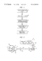
- FIG. 1 is a block diagram of the steps involved in imaging a semiconductor device in accordance with the invention
- FIG. 2 is a schematic diagram of apparatus useful in practicing the method of FIG. 1;
- FIG. 3 is a simplified energy band diagram of a typical semiconductor useful in explaining the method of FIG. 1;
- FIG. 4 illustrates the electronic control and measurement portion of the FIG. 3 apparatus
- FIGS. 5, 6 and 7 are exemplary images made in accordance with the method of FIG. 1 of an integrated circuit device.
- FIG. 1 is a block diagram of a method for imaging a semiconductor device in accordance with the invention.
- the first step is to provide a semiconductor device in suitable presentation for imaging.
- the device is in the form of a semiconductor chip, such as a monocrystalline silicon chip, having its active components formed adjacent an upper planar surface.
- These components can include various impurity-doped regions defining electronic devices such as resistors, capacitors or transistors or photoelectronic devices such as LEDs, solid state lasers or planar waveguides.
- the devices could be imaged either from above the active surface or from below through the underlying substrate.
- optical access from the top is often blocked by overlying layers of metallization. While the metal can be removed, such removal will often damage the structures to be observed. So the device components will be imaged from below, through the substrate.
- FIG. 2 which is a schematic diagram of preferred apparatus for practicing the method of FIG. 1, illustrates a preferred presentation of the semiconductor device 20 embedded in a plastic body 201 with the substrate bottom 202 exposed for viewing and a component-rich upper surface 203 embedded within the plastic.
- Conductive leads 204 , 205 to electrodes across the region to be imaged are extended out of the plastic.
- the surface with substrate bottom 202 is advantageously polished to a mirror finish.
- the next step shown in block B is to expose the device to light at a wavelength which is normally not absorbed by the substrate but which, in sufficient intensity, will be absorbed by two-photon absorption.
- FIG. 3 schematically illustrates the well-known energy band characteristic of crystalline semiconductors.
- the energy difference between these bands is the gap energy E.
- Light 33 having a photon energy hf 1 greater than the gap energy E can excite electrons from the valence band (leaving conductive “holes”) to the conduction band, so such light can be absorbed.
- Light 34 having photon energy hf 2 less than the gap energy E will not normally excite an electron transition. Such light at normal intensities will pass through the semiconductor unattenuated. However, if the energy of two photons is greater than E, i.e. 2hf 2 >E, then at sufficient intensity some electrons will simultaneously absorb two photons 35 , 36 and be excited from the valence band to the conduction band thereby generating charge carriers and current.
- the light shone on the device is concentrated to achieve two-photon absorption without damaging the device being imaged.
- this means that the light is concentrated in space, as by focusing. It is also advantageously concentrated in time as by the use of a pulsed laser light source. It is an advantage of this method that light will pass through the semiconductor substrate essentially unattenuated until it is sufficiently concentrated at the point of focus to excite two-photon absorption.
- control of the depth of focus one can choose the depth into the device of the region being examined. It is thus possible to image a particular planar region of interest, or by examining successively displaced planar regions, to generate a three-dimensional image of the device.
- the final step, shown in block E, is to create an image of the region scanned based on the current generated at each beam location. This is advantageously done using a computer to simultaneously control the scan and to receive the measured current for each scan location.
- FIG. 2 schematically illustrates a preferred apparatus for imaging a semiconductor device 20 comprising an illumination source 21 for providing a beam of light at a non-absorbing frequency ⁇ that will absorb in two-photon absorption (hf ⁇ 2hf).
- the source 21 can conveniently comprise a pump laser 210 , an optical parametric oscillator 211 , and an attenuator 212 for controlling the illumination intensity.
- the laser 210 is a modelocked femtosecond Ti: sapphire pulsed laser marketed by Spectra Physics under the tradename Tsunami.
- the oscillator 211 is an optical parametric oscillator marketed by Spectra Physics, Mountainview, Calif. under the tradename Opal.
- the attenuator can be a 50G00AV.1 from the Newport Corporation, Irvine, Calif.
- an exemplary excitation pulse width is 120 fs, the repetition rate can be 80 Mhz and the wavelength should be longer than 1.2 micrometers to avoid single—photon absorption.
- the wavelength is in the range 1.6 to 1.2 micrometers.
- the optical excitation can be provided by other sources such as pulsed sub-picosecond lasers developed for telecommunications applications in the 1300 nm and 1550 nm wavelength regions.
- a scanner 22 is provided for scanning the beam 23 over the device to be imaged.
- a preferred scanner is a raster scanner composed of two scan mirrors such as a 6800 Minor Positioning System marketed by Cambridge Technology, Inc., Watertown, Mass.
- Relay lenses 24 A, 24 B are advantageously provided for imaging the scan mirrors to the back aperture of an objective lens 25 .
- the relay lenses also serve to control the beam diameter. Suitable relay lenses are available from Spindler & Hoyer Inc.
- the objective lens 25 focuses the illumination beam 23 on the desired region of the device 20 .
- a light source suitable for exciting twophoton absorption such as source 21 , above, is substituted for the OEM light source.
- the computer software with these commercial microscopes can be used in forming the two-photon image.
- a ⁇ A741 operational amplifier chip from Texas Instruments was prepared for presentation as shown in FIG. 2 .
- the amplifier bias current of the chip 40 was connected via amplifier 41 and A/D converter 42 to the same computer 43 used to control the scanner 44 .
- the computer thus has the position and current information for processing the desired image.
- FIG. 5 depicts an image generated using a 10 ⁇ /0.3 NA objective lens.
- Image brightness illustrates the induced current level.
- Current can be of either polarity, with areas of the integrated circuit darker than background indicating a current out of the negative input.
- Edge enhancement has been used in this view. The arrow marks a transistor.
- FIG. 6 depicts the marked transistor at higher magnification taken with a 100 ⁇ /1.3 NA oil immersion lens. No edge enhancement was used.
- FIG. 7 is a higher magnification view of the boxed portion of FIG. 6 .
Abstract
Description
Claims (6)
Priority Applications (6)
| Application Number | Priority Date | Filing Date | Title |
|---|---|---|---|
| US08/856,561 US6316950B1 (en) | 1997-05-15 | 1997-05-15 | Method and apparatus for imaging semiconductor devices |
| TW087105344A TW369725B (en) | 1997-05-15 | 1998-04-09 | Method and apparatus for imaging semiconductor devices |
| EP98303500A EP0878841B1 (en) | 1997-05-15 | 1998-05-05 | Method for imaging semiconductor devices |
| DE69830946T DE69830946T2 (en) | 1997-05-15 | 1998-05-05 | Method for imaging semiconductor devices |
| KR1019980017633A KR100271843B1 (en) | 1997-05-15 | 1998-05-15 | Method and apparatus for imaging semiconductor device |
| JP13289498A JP3217750B2 (en) | 1997-05-15 | 1998-05-15 | Semiconductor device imaging method |
Applications Claiming Priority (1)
| Application Number | Priority Date | Filing Date | Title |
|---|---|---|---|
| US08/856,561 US6316950B1 (en) | 1997-05-15 | 1997-05-15 | Method and apparatus for imaging semiconductor devices |
Publications (1)
| Publication Number | Publication Date |
|---|---|
| US6316950B1 true US6316950B1 (en) | 2001-11-13 |
Family
ID=25323953
Family Applications (1)
| Application Number | Title | Priority Date | Filing Date |
|---|---|---|---|
| US08/856,561 Expired - Lifetime US6316950B1 (en) | 1997-05-15 | 1997-05-15 | Method and apparatus for imaging semiconductor devices |
Country Status (6)
| Country | Link |
|---|---|
| US (1) | US6316950B1 (en) |
| EP (1) | EP0878841B1 (en) |
| JP (1) | JP3217750B2 (en) |
| KR (1) | KR100271843B1 (en) |
| DE (1) | DE69830946T2 (en) |
| TW (1) | TW369725B (en) |
Cited By (9)
| Publication number | Priority date | Publication date | Assignee | Title |
|---|---|---|---|---|
| US6542180B1 (en) * | 2000-01-07 | 2003-04-01 | Mitutoyo Corporation | Systems and methods for adjusting lighting of a part based on a plurality of selected regions of an image of the part |
| US6563324B1 (en) * | 2000-11-30 | 2003-05-13 | Cognex Technology And Investment Corporation | Semiconductor device image inspection utilizing rotation invariant scale invariant method |
| US20030155482A1 (en) * | 2002-02-20 | 2003-08-21 | Leica Microsystems Heidelberg Gmbh | Microscope, detector, and method for microscopy |
| US20060165272A1 (en) * | 2002-07-09 | 2006-07-27 | Saloma Caesar A | Method for generating high-contrast images of semiconductor sites via one-photon optical beaminduced current imaging and confocal reflectance microscopy |
| US20120056626A1 (en) * | 2010-09-08 | 2012-03-08 | Dcg Systems, Inc. | Laser assisted device alteration using two-photon absorption |
| WO2013188046A1 (en) * | 2012-05-16 | 2013-12-19 | Dcg Systems, Inc. | Laser-assisted device alteration using synchronized laser pulses |
| US9201096B2 (en) | 2010-09-08 | 2015-12-01 | Dcg Systems, Inc. | Laser-assisted device alteration using synchronized laser pulses |
| US9733297B2 (en) | 2013-02-19 | 2017-08-15 | Hamamatsu Photonics K.K. | Electric field concentration location observation device and electric field concentration location observation method |
| US10191111B2 (en) | 2013-03-24 | 2019-01-29 | Dcg Systems, Inc. | Synchronized pulsed LADA for the simultaneous acquisition of timing diagrams and laser-induced upsets |
Families Citing this family (2)
| Publication number | Priority date | Publication date | Assignee | Title |
|---|---|---|---|---|
| JP2010181288A (en) * | 2009-02-05 | 2010-08-19 | Renesas Electronics Corp | Analyzer and analysis method of semiconductor integrated circuit |
| WO2021250984A1 (en) | 2020-06-08 | 2021-12-16 | 浜松ホトニクス株式会社 | Semiconductor inspecting method and semiconductor inspecting device |
Citations (6)
| Publication number | Priority date | Publication date | Assignee | Title |
|---|---|---|---|---|
| US4346348A (en) * | 1980-02-28 | 1982-08-24 | The United States Of America As Represented By The Secretary Of The Navy | Laser technique for accurately determining the compensation density in N-type narrow gap semiconductor |
| US5034613A (en) | 1989-11-14 | 1991-07-23 | Cornell Research Foundation, Inc. | Two-photon laser microscopy |
| US5289407A (en) | 1991-07-22 | 1994-02-22 | Cornell Research Foundation, Inc. | Method for three dimensional optical data storage and retrieval |
| US5334540A (en) | 1991-11-14 | 1994-08-02 | Mitsubishi Denki Kabushiki Kaisha | OBIC observation method and apparatus therefor |
| US5430305A (en) * | 1994-04-08 | 1995-07-04 | The United States Of America As Represented By The United States Department Of Energy | Light-induced voltage alteration for integrated circuit analysis |
| DE19609521A1 (en) | 1995-03-16 | 1996-09-19 | Mitsubishi Electric Corp | Photo-induced current detection scanning analyser for LSI pre-testing |
-
1997
- 1997-05-15 US US08/856,561 patent/US6316950B1/en not_active Expired - Lifetime
-
1998
- 1998-04-09 TW TW087105344A patent/TW369725B/en not_active IP Right Cessation
- 1998-05-05 DE DE69830946T patent/DE69830946T2/en not_active Expired - Lifetime
- 1998-05-05 EP EP98303500A patent/EP0878841B1/en not_active Expired - Lifetime
- 1998-05-15 KR KR1019980017633A patent/KR100271843B1/en active IP Right Grant
- 1998-05-15 JP JP13289498A patent/JP3217750B2/en not_active Expired - Fee Related
Patent Citations (6)
| Publication number | Priority date | Publication date | Assignee | Title |
|---|---|---|---|---|
| US4346348A (en) * | 1980-02-28 | 1982-08-24 | The United States Of America As Represented By The Secretary Of The Navy | Laser technique for accurately determining the compensation density in N-type narrow gap semiconductor |
| US5034613A (en) | 1989-11-14 | 1991-07-23 | Cornell Research Foundation, Inc. | Two-photon laser microscopy |
| US5289407A (en) | 1991-07-22 | 1994-02-22 | Cornell Research Foundation, Inc. | Method for three dimensional optical data storage and retrieval |
| US5334540A (en) | 1991-11-14 | 1994-08-02 | Mitsubishi Denki Kabushiki Kaisha | OBIC observation method and apparatus therefor |
| US5430305A (en) * | 1994-04-08 | 1995-07-04 | The United States Of America As Represented By The United States Department Of Energy | Light-induced voltage alteration for integrated circuit analysis |
| DE19609521A1 (en) | 1995-03-16 | 1996-09-19 | Mitsubishi Electric Corp | Photo-induced current detection scanning analyser for LSI pre-testing |
Cited By (16)
| Publication number | Priority date | Publication date | Assignee | Title |
|---|---|---|---|---|
| US6542180B1 (en) * | 2000-01-07 | 2003-04-01 | Mitutoyo Corporation | Systems and methods for adjusting lighting of a part based on a plurality of selected regions of an image of the part |
| US6563324B1 (en) * | 2000-11-30 | 2003-05-13 | Cognex Technology And Investment Corporation | Semiconductor device image inspection utilizing rotation invariant scale invariant method |
| US20030155482A1 (en) * | 2002-02-20 | 2003-08-21 | Leica Microsystems Heidelberg Gmbh | Microscope, detector, and method for microscopy |
| US6952006B2 (en) * | 2002-02-20 | 2005-10-04 | Leica Microsystems Heidelberg Gmbh | Microscope, detector, and method for microscopy |
| US20060165272A1 (en) * | 2002-07-09 | 2006-07-27 | Saloma Caesar A | Method for generating high-contrast images of semiconductor sites via one-photon optical beaminduced current imaging and confocal reflectance microscopy |
| US7235988B2 (en) * | 2002-07-09 | 2007-06-26 | Caesar A. Saloma | Method for generating high-contrast images of semiconductor sites via one-photon optical beam-induced current imaging and confocal reflectance microscopy |
| US8860447B2 (en) * | 2010-09-08 | 2014-10-14 | Dcg Systems, Inc. | Laser assisted device alteration using two-photon absorption |
| US20120056626A1 (en) * | 2010-09-08 | 2012-03-08 | Dcg Systems, Inc. | Laser assisted device alteration using two-photon absorption |
| US9201096B2 (en) | 2010-09-08 | 2015-12-01 | Dcg Systems, Inc. | Laser-assisted device alteration using synchronized laser pulses |
| US10209274B2 (en) | 2010-09-08 | 2019-02-19 | Fei Efa, Inc. | Laser-assisted device alteration using synchronized laser pulses |
| US11353479B2 (en) | 2010-09-08 | 2022-06-07 | Fei Efa, Inc. | Laser-assisted device alteration using synchronized laser pulses |
| WO2013188046A1 (en) * | 2012-05-16 | 2013-12-19 | Dcg Systems, Inc. | Laser-assisted device alteration using synchronized laser pulses |
| TWI479167B (en) * | 2012-05-16 | 2015-04-01 | Dcg Systems Inc | System and method laser-assisted device alteration using synchronized laser pulses |
| US9733297B2 (en) | 2013-02-19 | 2017-08-15 | Hamamatsu Photonics K.K. | Electric field concentration location observation device and electric field concentration location observation method |
| US10191111B2 (en) | 2013-03-24 | 2019-01-29 | Dcg Systems, Inc. | Synchronized pulsed LADA for the simultaneous acquisition of timing diagrams and laser-induced upsets |
| US11047906B2 (en) | 2013-03-24 | 2021-06-29 | Dcg Systems, Inc. | Synchronized pulsed LADA for the simultaneous acquisition of timing diagrams and laser-induced upsets |
Also Published As
| Publication number | Publication date |
|---|---|
| DE69830946D1 (en) | 2005-09-01 |
| JP3217750B2 (en) | 2001-10-15 |
| KR100271843B1 (en) | 2001-01-15 |
| KR19980087127A (en) | 1998-12-05 |
| EP0878841A3 (en) | 2000-02-23 |
| EP0878841B1 (en) | 2005-07-27 |
| EP0878841A2 (en) | 1998-11-18 |
| TW369725B (en) | 1999-09-11 |
| JPH10332794A (en) | 1998-12-18 |
| DE69830946T2 (en) | 2006-04-20 |
Similar Documents
| Publication | Publication Date | Title |
|---|---|---|
| Xu et al. | Two-photon optical beam induced current imaging through the backside of integrated circuits | |
| KR100483357B1 (en) | Apparatus and method for detecting micro defects in semi-conductors | |
| US6316950B1 (en) | Method and apparatus for imaging semiconductor devices | |
| US5777342A (en) | Method and apparatus for microlithography | |
| JP4711251B2 (en) | Method and system for repairing a defective photomask | |
| US7781749B2 (en) | Beam irradiation apparatus with deep ultraviolet light emission device for lithographic pattern inspection system | |
| EP0168643A3 (en) | Device for the inspection of wafers | |
| US5334540A (en) | OBIC observation method and apparatus therefor | |
| US7656516B2 (en) | Pattern inspection apparatus | |
| Xu et al. | Comparison of one-and two-photon optical beam-induced current imaging | |
| US5451886A (en) | Method of evaluating lifetime of semiconductor material and apparatus for the same | |
| JP2916321B2 (en) | Method for detecting internal defects in multilayer semiconductor substrate, etc. | |
| US6466040B1 (en) | Three dimensional optical beam induced current (3-D-OBIC) | |
| Darracq et al. | Investigation on the single event burnout sensitive volume using two-photon absorption laser testing | |
| Xu et al. | Two-photon optical beam induced current (OBIC) imaging through the backside of integrated circuits | |
| Ramsay et al. | Investigation of the two-photon optical beam induced current effect in silicon integrated circuits | |
| Pang et al. | Semiconductor applications of the scanning optical microscope | |
| JPH05136240A (en) | Obic observation method and device thereof | |
| Rozgonyi | Semiconductor materials engineering via defect diagnostics | |
| Ziegler | Laser scan microscope and infrared laser scan microcope: two important tools for device testing | |
| CN114616643A (en) | Charged particle inspection system and method using multi-wavelength charge controller | |
| Xu et al. | Two-photon photocurrent imaging of vertical cavity surface emitting lasers | |
| Bergner et al. | Obic-Investigations Of Integrated Circuits Using A Laser Scanning Microscope With Different Excitation Wavelengths | |
| JP2832272B2 (en) | Crystal defect observation device | |
| Chin et al. | Single contact optical beam induced currents (SCOBIC)-technique and applications |
Legal Events
| Date | Code | Title | Description |
|---|---|---|---|
| AS | Assignment |
Owner name: LUCENT TECHNOLOGIES INC., NEW JERSEY Free format text: ASSIGNMENT OF ASSIGNORS INTEREST;ASSIGNORS:DENK, WINFRIED;XU, CHUNHUI;REEL/FRAME:008878/0229 Effective date: 19971110 |
|
| STCF | Information on status: patent grant |
Free format text: PATENTED CASE |
|
| FPAY | Fee payment |
Year of fee payment: 4 |
|
| FPAY | Fee payment |
Year of fee payment: 8 |
|
| FPAY | Fee payment |
Year of fee payment: 12 |
|
| AS | Assignment |
Owner name: DEUTSCHE BANK AG NEW YORK BRANCH, AS COLLATERAL AG Free format text: PATENT SECURITY AGREEMENT;ASSIGNORS:LSI CORPORATION;AGERE SYSTEMS LLC;REEL/FRAME:032856/0031 Effective date: 20140506 |
|
| AS | Assignment |
Owner name: AVAGO TECHNOLOGIES GENERAL IP (SINGAPORE) PTE. LTD Free format text: ASSIGNMENT OF ASSIGNORS INTEREST;ASSIGNOR:AGERE SYSTEMS LLC;REEL/FRAME:035365/0634 Effective date: 20140804 |
|
| AS | Assignment |
Owner name: LSI CORPORATION, CALIFORNIA Free format text: TERMINATION AND RELEASE OF SECURITY INTEREST IN PATENT RIGHTS (RELEASES RF 032856-0031);ASSIGNOR:DEUTSCHE BANK AG NEW YORK BRANCH, AS COLLATERAL AGENT;REEL/FRAME:037684/0039 Effective date: 20160201 Owner name: AGERE SYSTEMS LLC, PENNSYLVANIA Free format text: TERMINATION AND RELEASE OF SECURITY INTEREST IN PATENT RIGHTS (RELEASES RF 032856-0031);ASSIGNOR:DEUTSCHE BANK AG NEW YORK BRANCH, AS COLLATERAL AGENT;REEL/FRAME:037684/0039 Effective date: 20160201 |
|
| AS | Assignment |
Owner name: BANK OF AMERICA, N.A., AS COLLATERAL AGENT, NORTH CAROLINA Free format text: PATENT SECURITY AGREEMENT;ASSIGNOR:AVAGO TECHNOLOGIES GENERAL IP (SINGAPORE) PTE. LTD.;REEL/FRAME:037808/0001 Effective date: 20160201 Owner name: BANK OF AMERICA, N.A., AS COLLATERAL AGENT, NORTH Free format text: PATENT SECURITY AGREEMENT;ASSIGNOR:AVAGO TECHNOLOGIES GENERAL IP (SINGAPORE) PTE. LTD.;REEL/FRAME:037808/0001 Effective date: 20160201 |
|
| AS | Assignment |
Owner name: AVAGO TECHNOLOGIES GENERAL IP (SINGAPORE) PTE. LTD., SINGAPORE Free format text: TERMINATION AND RELEASE OF SECURITY INTEREST IN PATENTS;ASSIGNOR:BANK OF AMERICA, N.A., AS COLLATERAL AGENT;REEL/FRAME:041710/0001 Effective date: 20170119 Owner name: AVAGO TECHNOLOGIES GENERAL IP (SINGAPORE) PTE. LTD Free format text: TERMINATION AND RELEASE OF SECURITY INTEREST IN PATENTS;ASSIGNOR:BANK OF AMERICA, N.A., AS COLLATERAL AGENT;REEL/FRAME:041710/0001 Effective date: 20170119 |
|
| AS | Assignment |
Owner name: BELL SEMICONDUCTOR, LLC, ILLINOIS Free format text: ASSIGNMENT OF ASSIGNORS INTEREST;ASSIGNORS:AVAGO TECHNOLOGIES GENERAL IP (SINGAPORE) PTE. LTD.;BROADCOM CORPORATION;REEL/FRAME:044886/0608 Effective date: 20171208 |
|
| AS | Assignment |
Owner name: CORTLAND CAPITAL MARKET SERVICES LLC, AS COLLATERA Free format text: SECURITY INTEREST;ASSIGNORS:HILCO PATENT ACQUISITION 56, LLC;BELL SEMICONDUCTOR, LLC;BELL NORTHERN RESEARCH, LLC;REEL/FRAME:045216/0020 Effective date: 20180124 |
|
| AS | Assignment |
Owner name: BELL NORTHERN RESEARCH, LLC, ILLINOIS Free format text: RELEASE BY SECURED PARTY;ASSIGNOR:CORTLAND CAPITAL MARKET SERVICES LLC;REEL/FRAME:059720/0719 Effective date: 20220401 Owner name: BELL SEMICONDUCTOR, LLC, ILLINOIS Free format text: RELEASE BY SECURED PARTY;ASSIGNOR:CORTLAND CAPITAL MARKET SERVICES LLC;REEL/FRAME:059720/0719 Effective date: 20220401 Owner name: HILCO PATENT ACQUISITION 56, LLC, ILLINOIS Free format text: RELEASE BY SECURED PARTY;ASSIGNOR:CORTLAND CAPITAL MARKET SERVICES LLC;REEL/FRAME:059720/0719 Effective date: 20220401 |