US6324676B1 - FPGA customizable to accept selected macros - Google Patents
FPGA customizable to accept selected macros Download PDFInfo
- Publication number
- US6324676B1 US6324676B1 US09/232,021 US23202199A US6324676B1 US 6324676 B1 US6324676 B1 US 6324676B1 US 23202199 A US23202199 A US 23202199A US 6324676 B1 US6324676 B1 US 6324676B1
- Authority
- US
- United States
- Prior art keywords
- macro
- key
- fpga
- locked
- configuration
- Prior art date
- Legal status (The legal status is an assumption and is not a legal conclusion. Google has not performed a legal analysis and makes no representation as to the accuracy of the status listed.)
- Expired - Lifetime
Links
Images


Classifications
-
- G—PHYSICS
- G06—COMPUTING; CALCULATING OR COUNTING
- G06F—ELECTRIC DIGITAL DATA PROCESSING
- G06F21/00—Security arrangements for protecting computers, components thereof, programs or data against unauthorised activity
- G06F21/70—Protecting specific internal or peripheral components, in which the protection of a component leads to protection of the entire computer
- G06F21/71—Protecting specific internal or peripheral components, in which the protection of a component leads to protection of the entire computer to assure secure computing or processing of information
- G06F21/76—Protecting specific internal or peripheral components, in which the protection of a component leads to protection of the entire computer to assure secure computing or processing of information in application-specific integrated circuits [ASIC] or field-programmable devices, e.g. field-programmable gate arrays [FPGA] or programmable logic devices [PLD]
Definitions
- the present invention relates to programmable devices such as field programmable gate arrays (FPGAs). More specifically, the present invention relates to methods for programming and enabling licensed macros in an FPGA.
- FPGAs field programmable gate arrays
- programmable devices such as field programmable gate arrays (FPGAs) and programmable logic devices (PLDS), can incorporate ever-increasing numbers of functional blocks and more flexible interconnect structures to provide greater functionality and flexibility.
- FPGAs field programmable gate arrays
- PLDS programmable logic devices
- FIG. 1 is a simplified schematic diagram of a conventional FPGA 110 .
- FPGA 110 includes user logic circuits such as input/output blocks (IOBs), configurable logic blocks (CLBs), and programmable interconnect 130 , which contains programmable switch matrices (PSMs).
- IOBs input/output blocks
- CLBs configurable logic blocks
- PSMs programmable switch matrices
- Each IOB and CLB can be configured through configuration port 120 to perform a variety of functions.
- Programmable interconnect 130 can be configured to provide electrical connections between the various CLBs and IOBs by configuring the PSMs and other programmable interconnection points (PIPS, not shown) through configuration port 120 .
- the IOBs can be configured to drive output signals or to receive input signals from various pins (not shown) of FPGA 110 .
- FPGA 110 also includes dedicated internal logic.
- Dedicated internal logic performs specific functions and can only be minimally configured by a user.
- configuration port 120 is one example of dedicated internal logic.
- Other examples may include dedicated clock nets (not shown), power distribution grids (not shown), and boundary scan logic (i.e. IEEE Boundary Scan Standard 1149.1, not shown).
- FPGA 110 is illustrated with 16 CLBs, 16 IOBs, and 9 PSMs for clarity only. Actual FPGAs may contain thousands of CLBs, thousands of IOBs, and thousands of PSMs. The ratio of the number of CLBs, IOBS, and PSMs can also vary.
- FPGA 110 also includes dedicated configuration logic circuits to program the user logic circuits.
- each CLB, IOB, PSM, and PIP contains a configuration memory (not shown) which must be configured before each CLB, IOB, PSM, or PIP can perform a specified function.
- Some FPGAs may also include pre-configured logic circuits that are configured by the manufacturer to perform specific functions. For example, some FPGAs are pre-configured to include a PCI bus interface.
- the configuration memories within an FPGA use static random access memory (SRAM) cells.
- SRAM static random access memory
- the configuration memories of FPGA 110 are connected by a configuration structure (not shown) to configuration port 120 through a configuration access port (CAP) 125 .
- CAP configuration access port
- a configuration port (a set of pins used during the configuration process) provides an interface for external configuration devices to program the FPGA.
- the configuration memories are typically arranged in rows and columns. The columns are loaded from a frame register which is in turn sequentially loaded from one or more sequential bitstreams. (The frame register is part of the configuration structure referenced above.)
- configuration access port 125 is essentially a bus that couples configuration port 120 to the configuration structure of FPGA 110 .
- FIG. 2 illustrates a conventional method used to configure FPGA 110 .
- FPGA 110 is coupled to a configuration device 230 such as a serial programmable read only memory (SPROM), an electrically programmable read only memory (EPROM), or a microprocessor.
- Configuration port 120 receives configuration data, usually in the form of a configuration bitstream, from configuration device 230 .
- configuration port 120 contains a set of mode pins, a clock pin and a configuration data input pin.
- Configuration data from configuration device 230 is transferred serially to FPGA 110 through the configuration data input pin.
- configuration port 120 comprises a set of configuration data input pins to increase the data transfer rate between configuration device 230 and FPGA 110 by transferring data in parallel.
- configuration port 120 usually has no more than eight configuration data input pins. Further, some FPGAs allow configuration through a boundary scan chain. Specific examples for configuring various FPGAs can be found on pages 4-46 to 4-59 of “The Programmable Logic Data Book”, published in January 1998 by Xilinx, Inc., and available from Xilinx, Inc., 2100 Logic Drive, San Jose, Calif. 95124, which pages are incorporated herein by reference. Additional methods to program FPGAs are described by Lawman in commonly assigned, co-pending U.S. patent application Ser. No. 09/000,519, entitled “DECODER STRUCTURE AND METHOD FOR FPGA CONFIGURATION” by Gary R. Lawman, which is referenced above.
- the present invention uses on-chip keys, i.e., keys programmed into the chip, to unlock locked macros before the macros will function.
- macro vendors can freely distribute locked macros as long as the key to the macro is secure.
- a macro vendor locks a macro using a lock to create a locked macro.
- a corresponding key is placed within the FPGA in a write-only memory or a write and read once memory. (A read-once memory is a memory that can be read back only once, e.g., for manufacturing test purposes.)
- a decoder detects the locked macro and uses the key to unlock the locked macro.
- An FPGA in accordance with one embodiment of the present invention comprises a configuration port, a decoder coupled to the configuration port, a key table coupled to the decoder and the configuration port, and a configuration access port coupled to the decoder.
- the key table is a memory that is write-only from outside the FPGA.
- the key table has visible header sections and invisible key sections. The visible header sections can be written to and read from outside the FPGA via the configuration port. The invisible key sections are write-only from outside the FPGA.
- the macro vendor When an end user wishes to incorporate a locked macro from a macro vendor, the macro vendor pre-programs a key into the key table of the FPGA. The end user creates a design file incorporating the locked macro. The design file is then converted into configuration data for the FPGA. The configuration data is sent into the configuration port of the FPGA. The on-chip decoder processes the configuration data and detects the locked macro. When the locked macro is detected, the decoder uses the key in the key table to unlock the locked macro. If the key table does not contain a key able to unlock the locked macro, configuration of the FPGA fails. If additional locked macros are desired, the macro vendor can pre-program additional keys into the FPGA. Thus, a macro vendor can freely distribute the locked macros without concern of unlicensed use as long as the keys to the locked macro are secure.
- multiple macro vendors can safely distribute locked macros. For example, if an end user desires a first locked macro from a first macro vendor and a second locked macro from a second macro vendor, a key manager can prepare the FPGA by pre-programming both a first key, which is configured to unlock the first locked macro, and a second key, which is configured to unlock the second locked macro, into the key table of an FPGA. The key manager obtains the first key from the first macro vendor and the second key from the second macro vendor. The key manager must keep the keys confidential and secured away from the end user.
- the locked macros can be freely distributed to the end user, since the end user must purchase the keyed FGPA, i.e., an FPGA having the appropriate keys, from the key manager.
- the key manager can distribute appropriate licensing fees to the macro vendors.
- an end user is provided with a key programming tool.
- the key programming tool is used to pre-program keys into an FPGA.
- encrypted keys are distributed to the end user.
- the end user uses the key programming tool, which is configured to obtain authorization from a macro vendor to use the key. The end user is never given access to the decrypted key.
- the key programming tool may also be configured to notify the macro vendor that a key is being pre-programmed, so that the macro vendor can collect the appropriate licensing fee.
- the key programming tool obtains the keys directly from the macro vendor over a secure medium, such as a telephone line or an encrypted channel of a public network such as the internet.
- the present invention advantageously enables macro vendors to freely distribute locked macros without losing licensing fees. Because the licensing fees are secured, macro vendors are motivated to rapidly introduce new and improved macros for end users.
- the present invention will be more fully understood in view of the following description and drawings.
- FIG. 1 is a simplified schematic diagram of a conventional FPGA.
- FIG. 2 is a prior art schematic diagram of an FPGA configured with a configuration device.
- FIG. 3 is a schematic diagram of an FPGA in accordance with one embodiment of the present invention.
- FIG. 4 is a block diagram of a key table in accordance with another embodiment of the present invention.
- FIG. 5 illustrates a method of programming an FPGA in accordance with another embodiment of the present invention.
- FIG. 6 illustrates a method of programming an FPGA in accordance with another embodiment of the present invention.
- FIG. 7 illustrates a method of programming an FPGA in accordance with another embodiment of the present invention.
- FIG. 8 illustrates a method of programming an FPGA in accordance with another embodiment of the present invention.
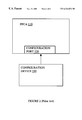
- FIG. 3 is a block diagram of an FPGA 300 in accordance with one embodiment of the present invention.
- the FPGA of FIG. 3 comprises a configuration port 320 , a decoder 330 , a key table 340 , and a configuration access port (CAP) 325 .
- Other standard PLD features such as CLBs, IOBs, and PSMs are included in FPGA 300 but are omitted in FIG. 3 for clarity.
- FPGA 300 routes the configuration data through decoder 330 before storing the configuration data into the configuration memories (not shown) of FPGA 300 .
- Decoder 330 processes the configuration data to locate locked macros.
- Locked macros are macros that are coded so that an FPGA can be programmed with the macro only if the FPGA was pre-programmed with the corresponding key. Alternatively, some locked macros can be loaded into an FPGA, but will only function if the FPGA contains the corresponding key. If decoder 330 detects a locked macro, decoder 330 attempts to use the pre-programmed keys from key table 340 to unlock the locked macro. If key table 340 contains an appropriate key, the locked macro is configured into FPGA 300 through configuration access port 325 .
- decoder 330 causes a configuration error and halts the configuration of FPGA 300 .
- the configuration of FPGA 300 proceeds to completion, but the locked macro does not function.
- Configuration data that is not part of a locked macro is stored in the appropriate configuration memories through configuration access port 325 .
- a detailed example of configuring locked macros in FPGA 300 is explained below with respect to FIG. 5 .
- public/private key encryption is used to lock the macros.
- public/private key encryption a message is encrypted using a public key to form an encrypted message. The message can only be decrypted by a private key that corresponds to the public key. Thus, the public key can be freely distributed, while the private key must be kept secret.
- a macro can be encrypted using a public key. The macro is then combined with the public key or a header indicating which public key was used for encryption to form a locked macro. A specific private key, which corresponds to the public key, is required to decrypt the locked macro. Thus, decoder 330 requires that the specific private key is accessible in key table 340 to unlock the locked macro.
- the public/private key system is not an integral part of the present invention.
- some embodiments of the present invention use asymmetric (public key) cryptosystems such as the RSA (Rivest, Shamir, Adleman) algorithm (which are implemented in PGP) or DSA (Digital Signature Algorithm), where the key used for encryption (public) is different from the key used for decryption (private).
- Other embodiments use symmetric (conventional, “secret key”) cryptosystems such as DES (Data Encryption Standard) or BLOWFISH, where the same key is used for both encryption and decryption.
- the terms public key and private key are not used further herein.
- the encrypting key is referred to as the lock, while the decrypting key is referred to simply as the key.
- the lock and the key i.e., the encrypting and decrypting keys) may be the same or they may be different.
- key table 340 is a memory that is write only from outside FPGA 300 . Decoder 330 can read key table 340 . However decoder 330 does not disclose the contents of key table 340 through configuration port 320 . Thus, once a key is placed in key table 340 of FPGA 300 , the key cannot be retrieved from FPGA 300 .
- key table 340 comprises FLASH RAM cells.
- FIG. 4 is a block diagram of key table 340 in accordance with a second embodiment of the present invention.
- the embodiment of FIG. 4 comprises four key registers 450 , 460 , 470 and 480 .
- Other embodiments of key table 340 may include hundreds or even thousands of key registers.
- Each key register comprises a visible header section and an invisible key section.
- key register 450 has a visible header section 453 and an invisible key section 457 .
- key registers 460 , 470 , and 480 have visible header sections 463 , 473 , and 483 , and invisible key sections 467 , 477 , and 487 , respectively.
- Visible header sections 453 , 463 , 473 , and 483 can be read from outside FPGA 300 through configuration port 320 .
- invisible key sections 457 , 467 , 477 , and 487 are write-only from outside FPGA 300 .
- a key can be tagged by a visible header to identify the key, while the actual key remains hidden in the invisible key sections.
- the visible header sections of key table 340 contain alpha-numeric description. For example, if the key for the Xilinx PCI macro is in invisible key section 457 , visible header section 453 is pre-programmed with “Xilinx PCI Macro”. Other embodiments use numeric codes to represent the macro vendor and the specific macro. Using a visible header allows an end user to determine which locked macros may be used with the FPGA.
- the visible header section is used as a content addressable memory to rapidly determine whether the key to a specific locked macro is stored in key table 340 .
- each locked macro contains information regarding the header of the appropriate key; for example, the numeric representation of the macro vendor and the numeric representation for the specific macro from the macro vendor.
- Decoder 330 (FIG. 3) can use the header information from the locked macro to address key table 340 to determine if the appropriate key resides in key table 340 .
- FIG. 5 illustrates how an FPGA is programmed with locked macros in accordance with one embodiment of the present invention.
- a user desires to use macro X and macro Y in an FPGA design.
- the vendor of macro X and macro Y provides locked macro 510 and locked macro 520 to the user.
- Locked macro 510 comprises lock XL and macro X, which is encrypted using lock XL.
- locked macro 520 comprises lock YL and macro Y, which is encrypted using lock YL.
- the user incorporates locked macros 510 and 520 into a design file 530 .
- Design file 530 is converted into configuration data 540 , which includes locked macro 510 _c, which is the converted version of locked macro 510 , and locked macro 520 _c, which is the converted version of locked macro 520 .
- the converted versions of the macros typically take the form of portions of a configuration bit stream, with the locks attached.
- Configuration data 540 is also typically a configuration bitstream.
- Configuration data 540 is fed into FPGA 300 through configuration port 320 .
- Decoder 330 processes configuration data 540 to determine if configuration data 540 contains any locked macros.
- decoder 330 detects locked macro 510 _c
- decoder 330 accesses key table 340 to determine if key table 340 contains a key to unlock locked macro 510 _c.
- key table 340 is pre-programmed to contain key XK which unlocks locked macro 510 _c.
- some embodiments encrypt macro X.
- decoder 330 decrypts macro X using key XK.
- the specific encryption algorithm is not an integral part of the present invention.
- decoder 330 uses key YK to unlock locked macro 520 _c. If key XK or key YK was not pre-programmed in key table 340 , configuration data 540 would fail to successfully configure FPGA 300 .
- FIG. 6 illustrates a method for distributing and using a locked macro 625 .
- a macro vendor 620 obtains an FPGA 615 from an FPGA maker 610 .
- middle men such as distributors and retailers, are omitted from FIG. 6 .
- Macro vendor 620 pre-programs FPGA 615 with an appropriate key for locked macro 625 to form keyed FPGA 623 .
- End user 630 purchases keyed FPGA 623 and locked macro 625 from macro vendor 620 .
- End user 630 then creates a programmed FPGA 635 containing locked macro 625 , using (for example) the method illustrated in FIG. 5 .
- each keyed FPGA can be customized for the end user to contain only keys for the specific locked macros desired by end user 630 .
- locked macro 625 can only be used with a properly keyed FPGA, (e.g., keyed FPGA 623 ), and because macro vendor 620 has sole control over the key for locked macro 625 , macro vendor 620 can prevent unlicensed end users from using locked macro 625 . If an unlicensed user obtained a copy of locked macro 625 , the unlicensed user still must obtain a properly keyed FPGA from macro vendor 620 to make use of locked macro 625 . Thus, macro vendor 620 can freely distribute copies of locked macro 625 .
- end user 630 cannot purchase keyed FPGA 623 from macro vendor 620 to use locked macro 625 , end user 630 cannot illicitly use locked macro 625 to produce unlicensed programmed FPGAs containing locked macro 625 .
- macro vendor 620 can provide locked macros to end users without fear of unlicensed use.
- an end user later decides that his design does not require locked macro 625 the end user can still use keyed FPGA 623 for his design.
- FIG. 7 illustrates a method in accordance with one embodiment of the present invention to safely distribute and use locked macros for multiple macro vendors.
- a key manager 740 obtains FPGA 615 from FPGA maker 610 .
- Key manager 740 also obtains keys from various macro vendors, such as key 624 (for locked macro 625 ) from macro vendor 620 and key 724 (for locked macro 725 ) from macro vendor 720 .
- End user 630 wishes to incorporate locked macros 625 and 725 into a design file. End user 630 can order keyed FPGA 745 from key manager 740 .
- Key manager 740 pre-programs the appropriate keys (i.e., keys 724 and 624 ), into keyed FPGA 745 , which is delivered to end user 630 .
- An important duty of key manager 740 is to insure that keys obtained from various macro vendors are kept confidential.
- key manager 740 is usually responsible for collecting licensing fees for macro vendor 720 and macro vendor 620 . Some FPGA makers may choose to perform the function of key manager 740 to better service macro vendors and end users.
- End user 630 obtains locked macro 725 from macro vendor 720 and locked macro 625 from macro vendor 620 .
- end user 630 has the desired locked macros for his design file and a properly keyed FPGA (i.e., keyed FPGA 745 ) to receive the design file.
- end user 630 can create a programmed FPGA 735 , which implements locked macro 725 from macro vendor 720 and locked macro 625 from macro vendor 620 .
- FIG. 8 illustrates a method in accordance with other embodiments of the present invention to safely distribute and use locked macros for multiple macro vendors.
- end user 630 obtains FPGA 615 from FPGA maker 610 .
- End user 630 also obtains locked macro 725 from macro vendor 720 and locked macro 625 from macro vendor 620 .
- End user 630 uses a key programming tool 830 to pre-program the appropriate keys into FPGA 615 .
- key programming tool contacts the appropriate macro vendor to obtain the desired key over a secure medium.
- key programming tool 830 contacts macro vendor 620 to obtain key 624 over secure medium 626 and contacts macro vendor 720 to obtain key 724 over secure medium 726 .
- the secure medium could be, for example, a telephone line to the macro vendors using modems, or an encrypted channel of a public network such as the internet.
- encrypted versions of keys 624 and 724 are distributed directly to end user 630 .
- key programming tool 830 can decrypt and pre-program FPGA 615 with keys 624 and 724 .
- Key programming tool 830 is configured to contact macro vendor 620 to obtain approval from macro vendor 620 before pre-programming key 624 into FPGA 615 .
- key programming tool 830 can be configured to notify macro vendor 620 each time an FPGA is pre-programmed with key 624 .
- key programming tool 830 is configured to contact macro vendor 720 before pre-programming FPGA 615 with key 724 .
- end user 630 can create programmed FPGA 735 using (for example) the method illustrated in FIG. 5 .
Abstract
A field programmable gate array (FPGA) is provided that can selectively accept or reject selected software (macros). Specifically, configuration data for the FPGA is passed through a configuration port to a decoder. The decoder processes the configuration data to detect locked macros. If a locked macro is detected, the decoder attempts to unlock the locked macro using one or more keys stored in a key table of the FGPA. If an appropriate key is in the key table, the decoder unlocks the locked macro to configure the FPGA. The keys can be pre-programmed into the FGPA by the macro vendor. If configuration data containing a locked macro is used with an FPGA without the appropriate key, configuration of the FPGA fails.
Description
This application relates to concurrently filed, co-pending U.S. patent application Ser. No. 09/232,022, “FPGA CUSTOMIZABLE TO ACCEPT SELECTED MACROS”, by Burnham et al., owned by the assignee of this application and incorporated herein by reference.
This application relates to concurrently filed, co-pending U.S. patent application Ser. No. 09/231,528, “METHOD TO SECURELY CONFIGURE AN FPGA USING ENCRYPTED MACRO”, by Burnham, owned by the assignee of this application and incorporated herein by reference.
This application relates to concurrently filed, co-pending U.S. patent application Ser. No. 09/231,912, “METHODS TO SECURELY CONFIGURE AN FPGA USING MACRO MARKERS”, by Burnham et. al., owned by the assignee of this application and incorporated herein by reference.
This application relates to U.S. patent application Ser. No. 09/000,519, entitled “DECODER STRUCTURE AND METHOD FOR FPGA CONFIGURATION” by Gary R. Lawman, which is also incorporated herein by reference.
The present invention relates to programmable devices such as field programmable gate arrays (FPGAs). More specifically, the present invention relates to methods for programming and enabling licensed macros in an FPGA.
Due to advancing semiconductor processing technology, integrated circuits have greatly increased in functionality and complexity. For example, programmable devices such as field programmable gate arrays (FPGAs) and programmable logic devices (PLDS), can incorporate ever-increasing numbers of functional blocks and more flexible interconnect structures to provide greater functionality and flexibility.
FIG. 1 is a simplified schematic diagram of a conventional FPGA 110. FPGA 110 includes user logic circuits such as input/output blocks (IOBs), configurable logic blocks (CLBs), and programmable interconnect 130, which contains programmable switch matrices (PSMs). Each IOB and CLB can be configured through configuration port 120 to perform a variety of functions. Programmable interconnect 130 can be configured to provide electrical connections between the various CLBs and IOBs by configuring the PSMs and other programmable interconnection points (PIPS, not shown) through configuration port 120. Typically, the IOBs can be configured to drive output signals or to receive input signals from various pins (not shown) of FPGA 110.
FPGA 110 also includes dedicated internal logic. Dedicated internal logic performs specific functions and can only be minimally configured by a user. For example, configuration port 120 is one example of dedicated internal logic. Other examples may include dedicated clock nets (not shown), power distribution grids (not shown), and boundary scan logic (i.e. IEEE Boundary Scan Standard 1149.1, not shown).
FPGA 110 also includes dedicated configuration logic circuits to program the user logic circuits. Specifically, each CLB, IOB, PSM, and PIP contains a configuration memory (not shown) which must be configured before each CLB, IOB, PSM, or PIP can perform a specified function. Some FPGAs may also include pre-configured logic circuits that are configured by the manufacturer to perform specific functions. For example, some FPGAs are pre-configured to include a PCI bus interface. Typically the configuration memories within an FPGA use static random access memory (SRAM) cells. The configuration memories of FPGA 110 are connected by a configuration structure (not shown) to configuration port 120 through a configuration access port (CAP) 125. A configuration port (a set of pins used during the configuration process) provides an interface for external configuration devices to program the FPGA. The configuration memories are typically arranged in rows and columns. The columns are loaded from a frame register which is in turn sequentially loaded from one or more sequential bitstreams. (The frame register is part of the configuration structure referenced above.) In FPGA 110, configuration access port 125 is essentially a bus that couples configuration port 120 to the configuration structure of FPGA 110.
FIG. 2 illustrates a conventional method used to configure FPGA 110. Specifically, FPGA 110 is coupled to a configuration device 230 such as a serial programmable read only memory (SPROM), an electrically programmable read only memory (EPROM), or a microprocessor. Configuration port 120 receives configuration data, usually in the form of a configuration bitstream, from configuration device 230. Typically, configuration port 120 contains a set of mode pins, a clock pin and a configuration data input pin. Configuration data from configuration device 230 is transferred serially to FPGA 110 through the configuration data input pin. In some embodiments of FPGA 110, configuration port 120 comprises a set of configuration data input pins to increase the data transfer rate between configuration device 230 and FPGA 110 by transferring data in parallel. However, due to the limited number of dedicated function pins available on an FPGA, configuration port 120 usually has no more than eight configuration data input pins. Further, some FPGAs allow configuration through a boundary scan chain. Specific examples for configuring various FPGAs can be found on pages 4-46 to 4-59 of “The Programmable Logic Data Book”, published in January 1998 by Xilinx, Inc., and available from Xilinx, Inc., 2100 Logic Drive, San Jose, Calif. 95124, which pages are incorporated herein by reference. Additional methods to program FPGAs are described by Lawman in commonly assigned, co-pending U.S. patent application Ser. No. 09/000,519, entitled “DECODER STRUCTURE AND METHOD FOR FPGA CONFIGURATION” by Gary R. Lawman, which is referenced above.
As explained above, actual FPGAs can have thousands of CLBs, IOBs, PSMs, and PIPs; therefore, the design and development of FPGA software is very time-consuming and expensive. Consequently, many vendors provide macros for various functions that can be incorporated by an end user of the FPGA into the user's own design file. For example, Xilinx, Inc. provides a PCI interface macro, which can be incorporated by an end user into the user's design file. The user benefits from the macro because the user does not need to spend the time or resources to develop the macro. Further, since the vendor profits from selling the same macro to many users, the vendor can spend the time and resources to design optimized macros. For example, the vendor strives to provide macros having high performance, flexibility, and low gate count. However, the macro vendors are reluctant to give out copies of the design macros without a way of insuring that the design macros are used only by licensed users. Hence, there is a need for a method or structure to insure third party macros are used only by licensed end users.
The present invention uses on-chip keys, i.e., keys programmed into the chip, to unlock locked macros before the macros will function. Thus, macro vendors can freely distribute locked macros as long as the key to the macro is secure. A macro vendor locks a macro using a lock to create a locked macro. A corresponding key is placed within the FPGA in a write-only memory or a write and read once memory. (A read-once memory is a memory that can be read back only once, e.g., for manufacturing test purposes.) During configuration of the FPGA, a decoder detects the locked macro and uses the key to unlock the locked macro.
An FPGA in accordance with one embodiment of the present invention comprises a configuration port, a decoder coupled to the configuration port, a key table coupled to the decoder and the configuration port, and a configuration access port coupled to the decoder. In one embodiment the key table is a memory that is write-only from outside the FPGA. However, in another embodiment, the key table has visible header sections and invisible key sections. The visible header sections can be written to and read from outside the FPGA via the configuration port. The invisible key sections are write-only from outside the FPGA.
When an end user wishes to incorporate a locked macro from a macro vendor, the macro vendor pre-programs a key into the key table of the FPGA. The end user creates a design file incorporating the locked macro. The design file is then converted into configuration data for the FPGA. The configuration data is sent into the configuration port of the FPGA. The on-chip decoder processes the configuration data and detects the locked macro. When the locked macro is detected, the decoder uses the key in the key table to unlock the locked macro. If the key table does not contain a key able to unlock the locked macro, configuration of the FPGA fails. If additional locked macros are desired, the macro vendor can pre-program additional keys into the FPGA. Thus, a macro vendor can freely distribute the locked macros without concern of unlicensed use as long as the keys to the locked macro are secure.
In accordance with another embodiment of the present invention, multiple macro vendors can safely distribute locked macros. For example, if an end user desires a first locked macro from a first macro vendor and a second locked macro from a second macro vendor, a key manager can prepare the FPGA by pre-programming both a first key, which is configured to unlock the first locked macro, and a second key, which is configured to unlock the second locked macro, into the key table of an FPGA. The key manager obtains the first key from the first macro vendor and the second key from the second macro vendor. The key manager must keep the keys confidential and secured away from the end user. The locked macros can be freely distributed to the end user, since the end user must purchase the keyed FGPA, i.e., an FPGA having the appropriate keys, from the key manager. The key manager can distribute appropriate licensing fees to the macro vendors.
In accordance with another embodiment of the present invention, an end user is provided with a key programming tool. The key programming tool is used to pre-program keys into an FPGA. In one embodiment, encrypted keys are distributed to the end user. The end user uses the key programming tool, which is configured to obtain authorization from a macro vendor to use the key. The end user is never given access to the decrypted key. The key programming tool may also be configured to notify the macro vendor that a key is being pre-programmed, so that the macro vendor can collect the appropriate licensing fee. In another embodiment, the key programming tool obtains the keys directly from the macro vendor over a secure medium, such as a telephone line or an encrypted channel of a public network such as the internet.
Thus, the present invention advantageously enables macro vendors to freely distribute locked macros without losing licensing fees. Because the licensing fees are secured, macro vendors are motivated to rapidly introduce new and improved macros for end users. The present invention will be more fully understood in view of the following description and drawings.
FIG. 1 is a simplified schematic diagram of a conventional FPGA.
FIG. 2 is a prior art schematic diagram of an FPGA configured with a configuration device.
FIG. 3 is a schematic diagram of an FPGA in accordance with one embodiment of the present invention.
FIG. 4 is a block diagram of a key table in accordance with another embodiment of the present invention.
FIG. 5 illustrates a method of programming an FPGA in accordance with another embodiment of the present invention.
FIG. 6 illustrates a method of programming an FPGA in accordance with another embodiment of the present invention.
FIG. 7 illustrates a method of programming an FPGA in accordance with another embodiment of the present invention.
FIG. 8 illustrates a method of programming an FPGA in accordance with another embodiment of the present invention.
FIG. 3 is a block diagram of an FPGA 300 in accordance with one embodiment of the present invention. The FPGA of FIG. 3 comprises a configuration port 320, a decoder 330, a key table 340, and a configuration access port (CAP) 325. Other standard PLD features such as CLBs, IOBs, and PSMs are included in FPGA 300 but are omitted in FIG. 3 for clarity. Unlike conventional FPGAs, FPGA 300 routes the configuration data through decoder 330 before storing the configuration data into the configuration memories (not shown) of FPGA 300.
In some embodiments, public/private key encryption is used to lock the macros. As is well known in the art, in public/private key encryption a message is encrypted using a public key to form an encrypted message. The message can only be decrypted by a private key that corresponds to the public key. Thus, the public key can be freely distributed, while the private key must be kept secret. For the present invention, a macro can be encrypted using a public key. The macro is then combined with the public key or a header indicating which public key was used for encryption to form a locked macro. A specific private key, which corresponds to the public key, is required to decrypt the locked macro. Thus, decoder 330 requires that the specific private key is accessible in key table 340 to unlock the locked macro.
The public/private key system is not an integral part of the present invention. For example, some embodiments of the present invention use asymmetric (public key) cryptosystems such as the RSA (Rivest, Shamir, Adleman) algorithm (which are implemented in PGP) or DSA (Digital Signature Algorithm), where the key used for encryption (public) is different from the key used for decryption (private). Other embodiments use symmetric (conventional, “secret key”) cryptosystems such as DES (Data Encryption Standard) or BLOWFISH, where the same key is used for both encryption and decryption. To avoid confusion, the terms public key and private key are not used further herein. Instead, the encrypting key is referred to as the lock, while the decrypting key is referred to simply as the key. The lock and the key (i.e., the encrypting and decrypting keys) may be the same or they may be different.
In one embodiment, key table 340 is a memory that is write only from outside FPGA 300. Decoder 330 can read key table 340. However decoder 330 does not disclose the contents of key table 340 through configuration port 320. Thus, once a key is placed in key table 340 of FPGA 300, the key cannot be retrieved from FPGA 300. In one embodiment, key table 340 comprises FLASH RAM cells.
FIG. 4 is a block diagram of key table 340 in accordance with a second embodiment of the present invention. The embodiment of FIG. 4 comprises four key registers 450, 460, 470 and 480. Other embodiments of key table 340 may include hundreds or even thousands of key registers. Each key register comprises a visible header section and an invisible key section. Specifically, key register 450 has a visible header section 453 and an invisible key section 457. Similarly, key registers 460, 470, and 480 have visible header sections 463, 473, and 483, and invisible key sections 467, 477, and 487, respectively. Visible header sections 453, 463, 473, and 483 can be read from outside FPGA 300 through configuration port 320. However, invisible key sections 457, 467, 477, and 487 are write-only from outside FPGA 300. Thus, for the embodiment of FIG. 4, a key can be tagged by a visible header to identify the key, while the actual key remains hidden in the invisible key sections. In one embodiment, the visible header sections of key table 340 contain alpha-numeric description. For example, if the key for the Xilinx PCI macro is in invisible key section 457, visible header section 453 is pre-programmed with “Xilinx PCI Macro”. Other embodiments use numeric codes to represent the macro vendor and the specific macro. Using a visible header allows an end user to determine which locked macros may be used with the FPGA.
In one embodiment, for large key tables, the visible header section is used as a content addressable memory to rapidly determine whether the key to a specific locked macro is stored in key table 340. Specifically, each locked macro contains information regarding the header of the appropriate key; for example, the numeric representation of the macro vendor and the numeric representation for the specific macro from the macro vendor. Decoder 330 (FIG. 3) can use the header information from the locked macro to address key table 340 to determine if the appropriate key resides in key table 340.
FIG. 5 illustrates how an FPGA is programmed with locked macros in accordance with one embodiment of the present invention. A user (not shown) desires to use macro X and macro Y in an FPGA design. The vendor of macro X and macro Y provides locked macro 510 and locked macro 520 to the user. Locked macro 510 comprises lock XL and macro X, which is encrypted using lock XL. Similarly, locked macro 520 comprises lock YL and macro Y, which is encrypted using lock YL. The user incorporates locked macros 510 and 520 into a design file 530. Design file 530 is converted into configuration data 540, which includes locked macro 510_c, which is the converted version of locked macro 510, and locked macro 520_c, which is the converted version of locked macro 520. The converted versions of the macros typically take the form of portions of a configuration bit stream, with the locks attached. Configuration data 540 is also typically a configuration bitstream.
Configuration data 540 is fed into FPGA 300 through configuration port 320. Decoder 330 processes configuration data 540 to determine if configuration data 540 contains any locked macros. When decoder 330 detects locked macro 510_c, decoder 330 accesses key table 340 to determine if key table 340 contains a key to unlock locked macro 510_c. In the example depicted in FIG. 5, key table 340 is pre-programmed to contain key XK which unlocks locked macro 510_c. As stated above, some embodiments encrypt macro X. For these embodiments, decoder 330 decrypts macro X using key XK. The specific encryption algorithm is not an integral part of the present invention. Similarly, when decoder 330 processes locked macro 520_c, decoder 330 uses key YK to unlock locked macro 520_c. If key XK or key YK was not pre-programmed in key table 340, configuration data 540 would fail to successfully configure FPGA 300.
FIG. 6 illustrates a method for distributing and using a locked macro 625. As illustrated in FIG. 6, a macro vendor 620 obtains an FPGA 615 from an FPGA maker 610. To avoid unnecessary confusion, middle men, such as distributors and retailers, are omitted from FIG. 6. Macro vendor 620 pre-programs FPGA 615 with an appropriate key for locked macro 625 to form keyed FPGA 623. End user 630 purchases keyed FPGA 623 and locked macro 625 from macro vendor 620. End user 630 then creates a programmed FPGA 635 containing locked macro 625, using (for example) the method illustrated in FIG. 5. If macro vendor 620 provides multiple locked macros, each keyed FPGA can be customized for the end user to contain only keys for the specific locked macros desired by end user 630. Because locked macro 625 can only be used with a properly keyed FPGA, (e.g., keyed FPGA 623), and because macro vendor 620 has sole control over the key for locked macro 625, macro vendor 620 can prevent unlicensed end users from using locked macro 625. If an unlicensed user obtained a copy of locked macro 625, the unlicensed user still must obtain a properly keyed FPGA from macro vendor 620 to make use of locked macro 625. Thus, macro vendor 620 can freely distribute copies of locked macro 625. Furthermore, because end user 630 must purchase keyed FPGA 623 from macro vendor 620 to use locked macro 625, end user 630 cannot illicitly use locked macro 625 to produce unlicensed programmed FPGAs containing locked macro 625. Thus, by using the method of FIG. 6, macro vendor 620 can provide locked macros to end users without fear of unlicensed use. In addition, if an end user later decides that his design does not require locked macro 625, the end user can still use keyed FPGA 623 for his design.
In many situations, an end user may wish to incorporate locked macros from multiple macro vendors into a single design file. FIG. 7 illustrates a method in accordance with one embodiment of the present invention to safely distribute and use locked macros for multiple macro vendors. As illustrated in FIG. 7, a key manager 740 obtains FPGA 615 from FPGA maker 610. Key manager 740 also obtains keys from various macro vendors, such as key 624 (for locked macro 625) from macro vendor 620 and key 724 (for locked macro 725) from macro vendor 720. End user 630 wishes to incorporate locked macros 625 and 725 into a design file. End user 630 can order keyed FPGA 745 from key manager 740. Key manager 740 pre-programs the appropriate keys (i.e., keys 724 and 624), into keyed FPGA 745, which is delivered to end user 630. An important duty of key manager 740 is to insure that keys obtained from various macro vendors are kept confidential. Furthermore, key manager 740 is usually responsible for collecting licensing fees for macro vendor 720 and macro vendor 620. Some FPGA makers may choose to perform the function of key manager 740 to better service macro vendors and end users.
End user 630 obtains locked macro 725 from macro vendor 720 and locked macro 625 from macro vendor 620. Thus, end user 630 has the desired locked macros for his design file and a properly keyed FPGA (i.e., keyed FPGA 745) to receive the design file. Thus, end user 630 can create a programmed FPGA 735, which implements locked macro 725 from macro vendor 720 and locked macro 625 from macro vendor 620.
FIG. 8 illustrates a method in accordance with other embodiments of the present invention to safely distribute and use locked macros for multiple macro vendors. As illustrated in FIG. 8, end user 630 obtains FPGA 615 from FPGA maker 610. End user 630 also obtains locked macro 725 from macro vendor 720 and locked macro 625 from macro vendor 620. End user 630 uses a key programming tool 830 to pre-program the appropriate keys into FPGA 615.
In one embodiment, key programming tool contacts the appropriate macro vendor to obtain the desired key over a secure medium. For example, in FIG. 8, key programming tool 830 contacts macro vendor 620 to obtain key 624 over secure medium 626 and contacts macro vendor 720 to obtain key 724 over secure medium 726. The secure medium could be, for example, a telephone line to the macro vendors using modems, or an encrypted channel of a public network such as the internet.
In another embodiment, encrypted versions of keys 624 and 724 are distributed directly to end user 630. However, only key programming tool 830 can decrypt and pre-program FPGA 615 with keys 624 and 724. Key programming tool 830 is configured to contact macro vendor 620 to obtain approval from macro vendor 620 before pre-programming key 624 into FPGA 615. Alternatively, key programming tool 830 can be configured to notify macro vendor 620 each time an FPGA is pre-programmed with key 624. Similarly, key programming tool 830 is configured to contact macro vendor 720 before pre-programming FPGA 615 with key 724. After pre-programming FPGA 615 with keys 724 and 624, end user 630 can create programmed FPGA 735 using (for example) the method illustrated in FIG. 5.
In the various embodiments of this invention, methods and structures have been described to securely distribute and use third party macros. By locking a macro so that a key is required in the FPGA to use the macro, macro vendors prevent unlicensed use of macros. Furthermore, by using a key manager or a key programming tool, an end user can easily incorporate macros from different macro vendors in a single FPGA design file. By providing a secure method to distribute macros, macro vendors are motivated to expend the time and effort to create large libraries of optimized macros to sell to end users. Thus, the cost and time for creating design files for FPGAs by an end user can be reduced through the use of macros from macro vendors.
The various embodiments of the structures and methods of this invention that are described above are illustrative only of the principles of this invention and are not intended to limit the scope of the invention to the particular embodiments described. For example, in view of this disclosure, those skilled in the art can define other decoders, locked macros, keys, key tables, key programming tools, configuration devices, FPGAs, CLBs, IOBs, PSMs, configuration access ports, configuration ports, and so forth, and use these alternative features to create a method, circuit, or system according to the principles of this invention. Thus, the invention is limited only by the following claims.
Claims (5)
1. A method for configuring a field programmable gate array (FPGA), the method comprising:
pre-programming a first key into a key table of said FPGA;
processing configuration data in said FPGA to detect a first locked macro; and
unlocking said first locked macro using said first key pre-programmed into said key table.
2. The method of claim 1, further comprising:
pre-programming a second key into a key table of said FPGA;
processing configuration data in said FPGA to detect a second locked macro; and
unlocking said second locked macro using said second key pre-programmed into said key table.
3. The method of claim 1, wherein the step of unlocking said first locked macro comprises the step of decrypting said first locked macro using said first key.
4. The method of claim 1, wherein said first key comprises a header section and a key section.
5. The method of claim 4, wherein the step of pre-programming a first key comprises:
storing said header section of said first key in a visible header section of said key table; and
storing said key section of said first key in an invisible key section of said key table.
Priority Applications (2)
| Application Number | Priority Date | Filing Date | Title |
|---|---|---|---|
| US09/232,021 US6324676B1 (en) | 1999-01-14 | 1999-01-14 | FPGA customizable to accept selected macros |
| US09/924,357 US6381732B1 (en) | 1999-01-14 | 2001-08-07 | FPGA customizable to accept selected macros |
Applications Claiming Priority (1)
| Application Number | Priority Date | Filing Date | Title |
|---|---|---|---|
| US09/232,021 US6324676B1 (en) | 1999-01-14 | 1999-01-14 | FPGA customizable to accept selected macros |
Related Child Applications (1)
| Application Number | Title | Priority Date | Filing Date |
|---|---|---|---|
| US09/924,357 Division US6381732B1 (en) | 1999-01-14 | 2001-08-07 | FPGA customizable to accept selected macros |
Publications (1)
| Publication Number | Publication Date |
|---|---|
| US6324676B1 true US6324676B1 (en) | 2001-11-27 |
Family
ID=22871559
Family Applications (2)
| Application Number | Title | Priority Date | Filing Date |
|---|---|---|---|
| US09/232,021 Expired - Lifetime US6324676B1 (en) | 1999-01-14 | 1999-01-14 | FPGA customizable to accept selected macros |
| US09/924,357 Expired - Lifetime US6381732B1 (en) | 1999-01-14 | 2001-08-07 | FPGA customizable to accept selected macros |
Family Applications After (1)
| Application Number | Title | Priority Date | Filing Date |
|---|---|---|---|
| US09/924,357 Expired - Lifetime US6381732B1 (en) | 1999-01-14 | 2001-08-07 | FPGA customizable to accept selected macros |
Country Status (1)
| Country | Link |
|---|---|
| US (2) | US6324676B1 (en) |
Cited By (25)
| Publication number | Priority date | Publication date | Assignee | Title |
|---|---|---|---|---|
| US20010037458A1 (en) * | 2000-02-08 | 2001-11-01 | Kean Thomas A. | Method of using a mask programmed key to securely configure a field programmable gate array |
| US6510548B1 (en) * | 2001-08-03 | 2003-01-21 | Xilinx, Inc. | Method for providing pre-designed modules for programmable logic devices |
| US20030068038A1 (en) * | 2001-09-28 | 2003-04-10 | Bedros Hanounik | Method and apparatus for encrypting data |
| US6581186B1 (en) * | 2000-05-31 | 2003-06-17 | Xilinx, Inc. | Methods and systems for providing logic cores from third party logic core providers |
| US20030204743A1 (en) * | 2002-04-16 | 2003-10-30 | Srinivas Devadas | Authentication of integrated circuits |
| US20040041175A1 (en) * | 2002-08-29 | 2004-03-04 | Anderson Howard C. | Apparatus for programming a programmable device, and method |
| US20040122643A1 (en) * | 2002-08-29 | 2004-06-24 | Anderson Howard C. | Apparatus and method for simulating switched-capacitor circuits |
| US7024654B2 (en) | 2002-06-11 | 2006-04-04 | Anadigm, Inc. | System and method for configuring analog elements in a configurable hardware device |
| US20060210082A1 (en) * | 2004-11-12 | 2006-09-21 | Srinivas Devadas | Volatile device keys and applications thereof |
| US7199608B1 (en) | 2005-02-17 | 2007-04-03 | Xilinx, Inc. | Programmable logic device and method of configuration |
| US7203842B2 (en) | 1999-12-22 | 2007-04-10 | Algotronix, Ltd. | Method and apparatus for secure configuration of a field programmable gate array |
| US20070088923A1 (en) * | 2004-03-08 | 2007-04-19 | Armstrong-Crews Nicholas L | System and method for fast, secure removal of objects from disk storage |
| US7219237B1 (en) * | 2002-03-29 | 2007-05-15 | Xilinx, Inc. | Read- and write-access control circuits for decryption-key memories on programmable logic devices |
| WO2007054251A2 (en) * | 2005-11-08 | 2007-05-18 | M2Ooo Sa | Configurable circuit with configuration data protection features |
| US20070288765A1 (en) * | 1999-12-22 | 2007-12-13 | Kean Thomas A | Method and Apparatus for Secure Configuration of a Field Programmable Gate Array |
| US20080270805A1 (en) * | 2001-06-13 | 2008-10-30 | Kean Thomas A | Method for Protecting Intellectual Property Cores on Field Programmable Gate Array |
| US20090083833A1 (en) * | 2007-09-19 | 2009-03-26 | Verayo, Inc. | Authentication with physical unclonable functions |
| US20090292978A1 (en) * | 2008-05-26 | 2009-11-26 | Fujitsu Limited | Configuration device for configuring FPGA |
| US20100127822A1 (en) * | 2008-11-21 | 2010-05-27 | Verayo, Inc. | Non-networked rfid-puf authentication |
| US20110033041A1 (en) * | 2009-08-05 | 2011-02-10 | Verayo, Inc. | Index-based coding with a pseudo-random source |
| US20110066670A1 (en) * | 2009-08-05 | 2011-03-17 | Verayo, Inc. | Combination of values from a pseudo-random source |
| US20120124255A1 (en) * | 2010-11-12 | 2012-05-17 | Invensys Systems Inc. | Priority Logic Module |
| US8630410B2 (en) | 2006-01-24 | 2014-01-14 | Verayo, Inc. | Signal generator based device security |
| US9483416B1 (en) * | 2010-10-21 | 2016-11-01 | Xilinx, Inc. | Secure processor operation using integrated circuit configuration circuitry |
| US9847980B2 (en) | 2015-06-17 | 2017-12-19 | Microsoft Technology Licensing, Llc | Protecting communications with hardware accelerators for increased workflow security |
Families Citing this family (76)
| Publication number | Priority date | Publication date | Assignee | Title |
|---|---|---|---|---|
| US7313705B2 (en) * | 2002-01-22 | 2007-12-25 | Texas Instrument Incorporated | Implementation of a secure computing environment by using a secure bootloader, shadow memory, and protected memory |
| US6976160B1 (en) * | 2002-02-22 | 2005-12-13 | Xilinx, Inc. | Method and system for controlling default values of flip-flops in PGA/ASIC-based designs |
| US6894527B1 (en) * | 2003-05-12 | 2005-05-17 | Xilinx, Inc. | Evolved circuits for bitstream protection |
| US7506377B2 (en) * | 2003-06-11 | 2009-03-17 | Hewlett-Packard Development Company, L.P. | Method and apparatus for playing content |
| US7440574B2 (en) * | 2003-06-11 | 2008-10-21 | Hewlett-Packard Development Company, L.P. | Content encryption using programmable hardware |
| US7219325B1 (en) * | 2003-11-21 | 2007-05-15 | Xilinx, Inc. | Exploiting unused configuration memory cells |
| US7126373B1 (en) | 2004-02-14 | 2006-10-24 | Herman Schmit | Configurable logic circuits with commutative properties |
| US7157933B1 (en) | 2004-02-14 | 2007-01-02 | Herman Schmit | Configurable circuits, IC's, and systems |
| US7284222B1 (en) | 2004-06-30 | 2007-10-16 | Tabula, Inc. | Method and apparatus for identifying connections between configurable nodes in a configurable integrated circuit |
| US7193432B1 (en) | 2004-02-14 | 2007-03-20 | Herman Schmit | VPA logic circuits |
| US7126381B1 (en) | 2004-02-14 | 2006-10-24 | Herman Schmit | VPA interconnect circuit |
| US7109752B1 (en) * | 2004-02-14 | 2006-09-19 | Herman Schmit | Configurable circuits, IC's, and systems |
| US7167025B1 (en) * | 2004-02-14 | 2007-01-23 | Herman Schmit | Non-sequentially configurable IC |
| US7193440B1 (en) | 2004-02-14 | 2007-03-20 | Herman Schmit | Configurable circuits, IC's, and systems |
| US7425841B2 (en) | 2004-02-14 | 2008-09-16 | Tabula Inc. | Configurable circuits, IC's, and systems |
| US7408382B2 (en) * | 2004-06-30 | 2008-08-05 | Tabula, Inc. | Configurable circuits, IC's, and systems |
| US7193438B1 (en) * | 2004-06-30 | 2007-03-20 | Andre Rohe | Configurable integrated circuit with offset connection |
| US7282950B1 (en) | 2004-11-08 | 2007-10-16 | Tabula, Inc. | Configurable IC's with logic resources with offset connections |
| US7449915B2 (en) * | 2004-06-30 | 2008-11-11 | Tabula Inc. | VPA logic circuits |
| US7145361B1 (en) * | 2004-06-30 | 2006-12-05 | Andre Rohe | Configurable integrated circuit with different connection schemes |
| US7312630B2 (en) * | 2004-06-30 | 2007-12-25 | Tabula, Inc. | Configurable integrated circuit with built-in turns |
| US7439766B2 (en) * | 2004-06-30 | 2008-10-21 | Tabula, Inc. | Configurable logic circuits with commutative properties |
| US7317331B2 (en) | 2004-11-08 | 2008-01-08 | Tabula, Inc. | Reconfigurable IC that has sections running at different reconfiguration rates |
| US7242216B1 (en) | 2004-11-08 | 2007-07-10 | Herman Schmit | Embedding memory between tile arrangement of a configurable IC |
| US20070244958A1 (en) * | 2004-11-08 | 2007-10-18 | Jason Redgrave | Configurable IC's with carry bypass circuitry |
| US7276933B1 (en) | 2004-11-08 | 2007-10-02 | Tabula, Inc. | Reconfigurable IC that has sections running at different looperness |
| US7224181B1 (en) * | 2004-11-08 | 2007-05-29 | Herman Schmit | Clock distribution in a configurable IC |
| US7301368B2 (en) * | 2005-03-15 | 2007-11-27 | Tabula, Inc. | Embedding memory within tile arrangement of a configurable IC |
| US7330050B2 (en) | 2004-11-08 | 2008-02-12 | Tabula, Inc. | Storage elements for a configurable IC and method and apparatus for accessing data stored in the storage elements |
| US7743085B2 (en) * | 2004-11-08 | 2010-06-22 | Tabula, Inc. | Configurable IC with large carry chains |
| US7295037B2 (en) * | 2004-11-08 | 2007-11-13 | Tabula, Inc. | Configurable IC with routing circuits with offset connections |
| US7573296B2 (en) | 2004-11-08 | 2009-08-11 | Tabula Inc. | Configurable IC with configurable routing resources that have asymmetric input and/or outputs |
| US7342415B2 (en) | 2004-11-08 | 2008-03-11 | Tabula, Inc. | Configurable IC with interconnect circuits that also perform storage operations |
| US7268586B1 (en) | 2004-11-08 | 2007-09-11 | Tabula, Inc. | Method and apparatus for accessing stored data in a reconfigurable IC |
| US7259587B1 (en) * | 2004-11-08 | 2007-08-21 | Tabula, Inc. | Configurable IC's with configurable logic resources that have asymetric inputs and/or outputs |
| US7917559B2 (en) * | 2004-11-08 | 2011-03-29 | Tabula, Inc. | Configurable IC's with configurable logic circuits that perform adder and/or subtractor operations |
| US7236009B1 (en) * | 2004-12-01 | 2007-06-26 | Andre Rohe | Operational time extension |
| US7428721B2 (en) * | 2004-12-01 | 2008-09-23 | Tabula, Inc. | Operational cycle assignment in a configurable IC |
| US7496879B2 (en) * | 2004-12-01 | 2009-02-24 | Tabula, Inc. | Concurrent optimization of physical design and operational cycle assignment |
| US7825684B2 (en) * | 2005-03-15 | 2010-11-02 | Tabula, Inc. | Variable width management for a memory of a configurable IC |
| US7230869B1 (en) | 2005-03-15 | 2007-06-12 | Jason Redgrave | Method and apparatus for accessing contents of memory cells |
| US7530033B2 (en) | 2005-03-15 | 2009-05-05 | Tabula, Inc. | Method and apparatus for decomposing functions in a configurable IC |
| US7310003B2 (en) * | 2005-03-15 | 2007-12-18 | Tabula, Inc. | Configurable IC with interconnect circuits that have select lines driven by user signals |
| US7298169B2 (en) * | 2005-03-15 | 2007-11-20 | Tabula, Inc | Hybrid logic/interconnect circuit in a configurable IC |
| US20070244959A1 (en) * | 2005-03-15 | 2007-10-18 | Steven Teig | Configurable IC's with dual carry chains |
| US7224182B1 (en) * | 2005-03-15 | 2007-05-29 | Brad Hutchings | Hybrid configurable circuit for a configurable IC |
| US7548085B2 (en) | 2005-07-15 | 2009-06-16 | Tabula, Inc. | Random access of user design states in a configurable IC |
| DE602005021120D1 (en) * | 2005-10-28 | 2010-06-17 | Emma Mixed Signal Cv | Access control to a decryption table of ASIC or ASSP |
| US8463836B1 (en) | 2005-11-07 | 2013-06-11 | Tabula, Inc. | Performing mathematical and logical operations in multiple sub-cycles |
| US7765249B1 (en) | 2005-11-07 | 2010-07-27 | Tabula, Inc. | Use of hybrid interconnect/logic circuits for multiplication |
| US7372297B1 (en) | 2005-11-07 | 2008-05-13 | Tabula Inc. | Hybrid interconnect/logic circuits enabling efficient replication of a function in several sub-cycles to save logic and routing resources |
| US7818361B1 (en) | 2005-11-07 | 2010-10-19 | Tabula, Inc. | Method and apparatus for performing two's complement multiplication |
| US7489162B1 (en) | 2005-12-01 | 2009-02-10 | Tabula, Inc. | Users registers in a reconfigurable IC |
| US7461362B1 (en) | 2005-12-01 | 2008-12-02 | Tabula, Inc. | Replacing circuit design elements with their equivalents |
| US7679401B1 (en) | 2005-12-01 | 2010-03-16 | Tabula, Inc. | User registers implemented with routing circuits in a configurable IC |
| US7504858B1 (en) | 2006-03-08 | 2009-03-17 | Tabula, Inc. | Configurable integrated circuit with parallel non-neighboring offset connections |
| US7694083B1 (en) * | 2006-03-08 | 2010-04-06 | Tabula, Inc. | System and method for providing a virtual memory architecture narrower and deeper than a physical memory architecture |
| US7609085B1 (en) | 2006-03-08 | 2009-10-27 | Tabula, Inc. | Configurable integrated circuit with a 4-to-1 multiplexer |
| US7518400B1 (en) | 2006-03-08 | 2009-04-14 | Tabula, Inc. | Barrel shifter implemented on a configurable integrated circuit |
| US7797497B1 (en) * | 2006-03-08 | 2010-09-14 | Tabula, Inc. | System and method for providing more logical memory ports than physical memory ports |
| US7529992B1 (en) | 2006-03-27 | 2009-05-05 | Tabula, Inc. | Configurable integrated circuit with error correcting circuitry |
| US7669097B1 (en) | 2006-03-27 | 2010-02-23 | Tabula, Inc. | Configurable IC with error detection and correction circuitry |
| US7930666B1 (en) | 2006-12-12 | 2011-04-19 | Tabula, Inc. | System and method of providing a memory hierarchy |
| US7587697B1 (en) | 2006-12-12 | 2009-09-08 | Tabula, Inc. | System and method of mapping memory blocks in a configurable integrated circuit |
| EP2140548A4 (en) * | 2007-03-20 | 2010-06-09 | Tabula Inc | Configurable ic having a routing fabric with storage elements |
| US7610566B1 (en) | 2007-03-22 | 2009-10-27 | Tabula, Inc. | Method and apparatus for function decomposition |
| US7636802B1 (en) * | 2007-04-11 | 2009-12-22 | Xilinx, Inc. | Data transfer using the configuration port of a programmable logic device |
| US8344755B2 (en) * | 2007-09-06 | 2013-01-01 | Tabula, Inc. | Configuration context switcher |
| US8990651B2 (en) * | 2007-09-19 | 2015-03-24 | Tabula, Inc. | Integrated circuit (IC) with primary and secondary networks and device containing such an IC |
| US8863067B1 (en) | 2008-02-06 | 2014-10-14 | Tabula, Inc. | Sequential delay analysis by placement engines |
| US8166435B2 (en) | 2008-06-26 | 2012-04-24 | Tabula, Inc. | Timing operations in an IC with configurable circuits |
| WO2010016857A1 (en) | 2008-08-04 | 2010-02-11 | Tabula, Inc. | Trigger circuits and event counters for an ic |
| EP2553815A1 (en) | 2010-04-02 | 2013-02-06 | Tabula, Inc. | System and method for reducing reconfiguration power usage |
| US8941409B2 (en) | 2011-07-01 | 2015-01-27 | Tabula, Inc. | Configurable storage elements |
| DE102011085487A1 (en) * | 2011-10-31 | 2013-05-02 | Rohde & Schwarz Gmbh & Co. Kg | Integrated circuit, has activation unit for activating technical functions, key generating unit for generating keys that identify circuit and/or functions, and comparator for comparing keys generated by generating unit with read key |
| US10482209B1 (en) | 2018-08-06 | 2019-11-19 | HLS Logix LLC | Field programmable operation block array |
Citations (20)
| Publication number | Priority date | Publication date | Assignee | Title |
|---|---|---|---|---|
| US3849760A (en) | 1971-07-12 | 1974-11-19 | Hitachi Ltd | Multi-dimensional pattern recognition processor |
| EP0253530A2 (en) | 1986-07-18 | 1988-01-20 | Honeywell Inc. | Dynamically reconfigurable array logic |
| US4849904A (en) * | 1987-06-19 | 1989-07-18 | International Business Machines Corporation | Macro structural arrangement and method for generating macros for VLSI semiconductor circuit devices |
| US5084636A (en) | 1989-12-27 | 1992-01-28 | Kawasaki Steel | Master-slave programmable logic devices |
| US5128871A (en) | 1990-03-07 | 1992-07-07 | Advanced Micro Devices, Inc. | Apparatus and method for allocation of resoures in programmable logic devices |
| WO1992020157A1 (en) | 1991-05-03 | 1992-11-12 | Lattice Semiconductor Corporation | Structure and method for multiplexing pins for in-system programming |
| US5197016A (en) * | 1988-01-13 | 1993-03-23 | International Chip Corporation | Integrated silicon-software compiler |
| US5237219A (en) | 1992-05-08 | 1993-08-17 | Altera Corporation | Methods and apparatus for programming cellular programmable logic integrated circuits |
| USRE34363E (en) | 1984-03-12 | 1993-08-31 | Xilinx, Inc. | Configurable electrical circuit having configurable logic elements and configurable interconnects |
| WO1994001867A1 (en) | 1992-07-02 | 1994-01-20 | Camarota Rafael C | Non-disruptive, randomly addressable memory system |
| WO1994010754A1 (en) | 1992-11-05 | 1994-05-11 | Xilinx, Inc. | Improved configurable cellular array |
| US5343406A (en) | 1989-07-28 | 1994-08-30 | Xilinx, Inc. | Distributed memory architecture for a configurable logic array and method for using distributed memory |
| US5352940A (en) * | 1993-05-27 | 1994-10-04 | Altera Corporation | Ram convertible look-up table based macrocell for PLDs |
| US5394031A (en) | 1993-12-08 | 1995-02-28 | At&T Corp. | Apparatus and method to improve programming speed of field programmable gate arrays |
| US5457408A (en) * | 1994-11-23 | 1995-10-10 | At&T Corp. | Method and apparatus for verifying whether a bitstream received by a field programmable gate array (FPGA) is intended for that FPGA |
| US5574655A (en) | 1991-10-30 | 1996-11-12 | Xilinx, Inc. | Method of allocating logic using general function components |
| US5705938A (en) | 1995-05-02 | 1998-01-06 | Xilinx, Inc. | Programmable switch for FPGA input/output signals |
| US5909658A (en) * | 1996-06-18 | 1999-06-01 | International Business Machines Corporation | High speed electron beam lithography pattern processing system |
| US5946478A (en) * | 1997-05-16 | 1999-08-31 | Xilinx, Inc. | Method for generating a secure macro element of a design for a programmable IC |
| US6205574B1 (en) * | 1998-07-28 | 2001-03-20 | Xilinx, Inc. | Method and system for generating a programming bitstream including identification bits |
Family Cites Families (3)
| Publication number | Priority date | Publication date | Assignee | Title |
|---|---|---|---|---|
| JPS6478023A (en) * | 1987-09-18 | 1989-03-23 | Fujitsu Ltd | Programmable logic device |
| US6028445A (en) | 1997-12-30 | 2000-02-22 | Xilinx, Inc. | Decoder structure and method for FPGA configuration |
| US6305005B1 (en) * | 1999-01-14 | 2001-10-16 | Xilinx, Inc. | Methods to securely configure an FPGA using encrypted macros |
-
1999
- 1999-01-14 US US09/232,021 patent/US6324676B1/en not_active Expired - Lifetime
-
2001
- 2001-08-07 US US09/924,357 patent/US6381732B1/en not_active Expired - Lifetime
Patent Citations (21)
| Publication number | Priority date | Publication date | Assignee | Title |
|---|---|---|---|---|
| US3849760A (en) | 1971-07-12 | 1974-11-19 | Hitachi Ltd | Multi-dimensional pattern recognition processor |
| USRE34363E (en) | 1984-03-12 | 1993-08-31 | Xilinx, Inc. | Configurable electrical circuit having configurable logic elements and configurable interconnects |
| EP0253530A2 (en) | 1986-07-18 | 1988-01-20 | Honeywell Inc. | Dynamically reconfigurable array logic |
| US4849904A (en) * | 1987-06-19 | 1989-07-18 | International Business Machines Corporation | Macro structural arrangement and method for generating macros for VLSI semiconductor circuit devices |
| US5197016A (en) * | 1988-01-13 | 1993-03-23 | International Chip Corporation | Integrated silicon-software compiler |
| US5343406A (en) | 1989-07-28 | 1994-08-30 | Xilinx, Inc. | Distributed memory architecture for a configurable logic array and method for using distributed memory |
| US5084636A (en) | 1989-12-27 | 1992-01-28 | Kawasaki Steel | Master-slave programmable logic devices |
| US5128871A (en) | 1990-03-07 | 1992-07-07 | Advanced Micro Devices, Inc. | Apparatus and method for allocation of resoures in programmable logic devices |
| WO1992020157A1 (en) | 1991-05-03 | 1992-11-12 | Lattice Semiconductor Corporation | Structure and method for multiplexing pins for in-system programming |
| US5237218A (en) | 1991-05-03 | 1993-08-17 | Lattice Semiconductor Corporation | Structure and method for multiplexing pins for in-system programming |
| US5574655A (en) | 1991-10-30 | 1996-11-12 | Xilinx, Inc. | Method of allocating logic using general function components |
| US5237219A (en) | 1992-05-08 | 1993-08-17 | Altera Corporation | Methods and apparatus for programming cellular programmable logic integrated circuits |
| WO1994001867A1 (en) | 1992-07-02 | 1994-01-20 | Camarota Rafael C | Non-disruptive, randomly addressable memory system |
| WO1994010754A1 (en) | 1992-11-05 | 1994-05-11 | Xilinx, Inc. | Improved configurable cellular array |
| US5352940A (en) * | 1993-05-27 | 1994-10-04 | Altera Corporation | Ram convertible look-up table based macrocell for PLDs |
| US5394031A (en) | 1993-12-08 | 1995-02-28 | At&T Corp. | Apparatus and method to improve programming speed of field programmable gate arrays |
| US5457408A (en) * | 1994-11-23 | 1995-10-10 | At&T Corp. | Method and apparatus for verifying whether a bitstream received by a field programmable gate array (FPGA) is intended for that FPGA |
| US5705938A (en) | 1995-05-02 | 1998-01-06 | Xilinx, Inc. | Programmable switch for FPGA input/output signals |
| US5909658A (en) * | 1996-06-18 | 1999-06-01 | International Business Machines Corporation | High speed electron beam lithography pattern processing system |
| US5946478A (en) * | 1997-05-16 | 1999-08-31 | Xilinx, Inc. | Method for generating a secure macro element of a design for a programmable IC |
| US6205574B1 (en) * | 1998-07-28 | 2001-03-20 | Xilinx, Inc. | Method and system for generating a programming bitstream including identification bits |
Non-Patent Citations (20)
| Title |
|---|
| "Core Solutions Data Book", published May, 1997, pp. 2-5 to 2-13 available from Xilinx, Inc., 2100 Logic Drive, San Jose, California 95124. |
| "IEEE Standard Test Access Port and Boundary-Scan Architecture", IEEE Std. 1149.1, published Oct. 21, 1993. |
| "New IEEE Standard Dictionary of Electrical and Electronics Terms", Fifth Edition, 1993, p. 1011. |
| "The Programmable Logic Data Book", published 1994, available from Xilinx, Inc., 2100 Logic Drive, San Jose, California 95124, pp. 2-105 to 2-132 and 2-231 to 2-238. |
| "The Programmable Logic Data Book", published 1998, available from Xilinx, Inc., 2100 Logic Drive, San Jose, California 95124, pp. 4-46 to 4-59. |
| "The Programmable Logic Data Book", published Sep., 1996, in its entirety and also specifically pp. 4-54 to 4-79 and 4-253 to 4-286, available from Xilinx, Inc., 2100 Logic Drive, San Jose, California 95124. |
| Betty Prince, "Semiconductor Memories", copyright 1983, 1991, John Wiley & Sons, pp. 149-174. |
| Box, "Field Programming Gate Array Based Configurable Preprocessor", Proceedings of the IEEE 1994 National Aerospace and Electronics Conference, May 23-27, 1994, NAECON 1994, vol. 1, pp. 427-434. |
| D.D. Gajski, et al., "Computer Architecture" IEEE Tutorial Manual, IEEE Computer Society, 1987, pp. v-i. |
| David A. Patterson and John L. Hennessy, "Computer Architecture: A Quantitive Approach", pp. 200-201, 1990. |
| Hodges, et al., "Analog MOS Integrated Circuits" IEEE Press, 1980, pp. 2-11. |
| Kean et al. ("DES key breaking, encryption and decryption on the XC6216", Proceedings of IEEE Symposium on FPGAs for Custom Computing Machines, 1998, Apr. 15, 1998, pp. 310-311).* |
| Kean et al., "DES Key Breaking, Encryption, and Decryption on the XC6216", Proceedings of IEEE Symposium on FPGAs for Custom Computing Machines, 1998, pp. 310-311. |
| McCarley et al., "Macro-Instruction Generation for Dynamic Logic Caching", Proceedings of the IEEE 1995 National Workshop on Rapid System Prototyping, Jun. 24-26, 1997, pp. 63-69. |
| Patriquin et al., "An Automated Design Process for the Champ Module", Proceedings of the IEEE 1995 National Aerospace and Electronics Conference, May 22-26, 1995, NAEC, vol. 1, pp. 427-434. |
| Runje et al. ("Universal strong encryption FPGA core implementation", Proceedings of Design, Automation and Test in Europe, 1998, Feb. 23, 1998, pp. 923-924).* |
| Runje et al., "Universal Strong Encryption FPGA Core Implementation", Proceedings of Design, Automation, and Test in Europe, 1998, pp. 923-924. |
| Shi et al., "Macro Block Based FPGA Floorplanning", Proceedings of the Tenth International Conference on VSLI Design, Jan. 4-7, 1997, pp. 21-26. |
| Wong et al. ("A single-chip FPGA implementation of the data encryption standard (DES) algorithm", IEEE Global Telecommunications Conference, 1998, GLOBECOM 1998, The Bridge to Global Integration, vol. 2, Nov. 8, 1998, pp. 827-832).* |
| Wong et al., "A single-Chip FPGA Implementation of the Data Encryption Standard (DES) Algorithm", IEEE Global Telecommunications Conference, 1998, GLOBECOM 1998, The Bridge to Global Integration, vol. 2, pp. 827-832. |
Cited By (54)
| Publication number | Priority date | Publication date | Assignee | Title |
|---|---|---|---|---|
| US7203842B2 (en) | 1999-12-22 | 2007-04-10 | Algotronix, Ltd. | Method and apparatus for secure configuration of a field programmable gate array |
| US20070288765A1 (en) * | 1999-12-22 | 2007-12-13 | Kean Thomas A | Method and Apparatus for Secure Configuration of a Field Programmable Gate Array |
| US20010037458A1 (en) * | 2000-02-08 | 2001-11-01 | Kean Thomas A. | Method of using a mask programmed key to securely configure a field programmable gate array |
| US7240218B2 (en) * | 2000-02-08 | 2007-07-03 | Algotronix, Ltd. | Method of using a mask programmed key to securely configure a field programmable gate array |
| US6581186B1 (en) * | 2000-05-31 | 2003-06-17 | Xilinx, Inc. | Methods and systems for providing logic cores from third party logic core providers |
| US20080270805A1 (en) * | 2001-06-13 | 2008-10-30 | Kean Thomas A | Method for Protecting Intellectual Property Cores on Field Programmable Gate Array |
| US6510548B1 (en) * | 2001-08-03 | 2003-01-21 | Xilinx, Inc. | Method for providing pre-designed modules for programmable logic devices |
| US20030068038A1 (en) * | 2001-09-28 | 2003-04-10 | Bedros Hanounik | Method and apparatus for encrypting data |
| US7389429B1 (en) | 2002-03-29 | 2008-06-17 | Xilinx, Inc. | Self-erasing memory for protecting decryption keys and proprietary configuration data |
| US7373668B1 (en) | 2002-03-29 | 2008-05-13 | Xilinx, Inc. | Methods and circuits for protecting proprietary configuration data for programmable logic devices |
| US7366306B1 (en) | 2002-03-29 | 2008-04-29 | Xilinx, Inc. | Programmable logic device that supports secure and non-secure modes of decryption-key access |
| US7219237B1 (en) * | 2002-03-29 | 2007-05-15 | Xilinx, Inc. | Read- and write-access control circuits for decryption-key memories on programmable logic devices |
| US7904731B2 (en) | 2002-04-16 | 2011-03-08 | Massachusetts Institute Of Technology | Integrated circuit that uses a dynamic characteristic of the circuit |
| US20090222672A1 (en) * | 2002-04-16 | 2009-09-03 | Massachusetts Institute Of Technology | Integrated Circuit That Uses A Dynamic Characteristic Of The Circuit |
| US8386801B2 (en) | 2002-04-16 | 2013-02-26 | Massachusetts Institute Of Technology | Authentication of integrated circuits |
| US20060271792A1 (en) * | 2002-04-16 | 2006-11-30 | Srinivas Devadas | Data protection and cryptographic functions using a device-specific value |
| US7840803B2 (en) | 2002-04-16 | 2010-11-23 | Massachusetts Institute Of Technology | Authentication of integrated circuits |
| US7681103B2 (en) | 2002-04-16 | 2010-03-16 | Massachusetts Institute Of Technology | Reliable generation of a device-specific value |
| US7818569B2 (en) | 2002-04-16 | 2010-10-19 | Massachusetts Institute Of Technology | Data protection and cryptographic functions using a device-specific value |
| US7757083B2 (en) | 2002-04-16 | 2010-07-13 | Massachusetts Institute Of Technology | Integrated circuit that uses a dynamic characteristic of the circuit |
| US20030204743A1 (en) * | 2002-04-16 | 2003-10-30 | Srinivas Devadas | Authentication of integrated circuits |
| US20060221686A1 (en) * | 2002-04-16 | 2006-10-05 | Srinivas Devadas | Integrated circuit that uses a dynamic characteristic of the circuit |
| US7024654B2 (en) | 2002-06-11 | 2006-04-04 | Anadigm, Inc. | System and method for configuring analog elements in a configurable hardware device |
| US6978435B2 (en) | 2002-08-29 | 2005-12-20 | Anadigm, Inc. | Apparatus for programming a programmable device, and method |
| US20040122643A1 (en) * | 2002-08-29 | 2004-06-24 | Anderson Howard C. | Apparatus and method for simulating switched-capacitor circuits |
| US20040041175A1 (en) * | 2002-08-29 | 2004-03-04 | Anderson Howard C. | Apparatus for programming a programmable device, and method |
| US7216207B1 (en) * | 2004-03-08 | 2007-05-08 | International Business Machines Corporation | System and method for fast, secure removal of objects from disk storage |
| US20070088923A1 (en) * | 2004-03-08 | 2007-04-19 | Armstrong-Crews Nicholas L | System and method for fast, secure removal of objects from disk storage |
| US7564345B2 (en) | 2004-11-12 | 2009-07-21 | Verayo, Inc. | Volatile device keys and applications thereof |
| US7839278B2 (en) | 2004-11-12 | 2010-11-23 | Verayo, Inc. | Volatile device keys and applications thereof |
| US20090254981A1 (en) * | 2004-11-12 | 2009-10-08 | Verayo, Inc. | Volatile Device Keys And Applications Thereof |
| US8756438B2 (en) | 2004-11-12 | 2014-06-17 | Verayo, Inc. | Securely field configurable device |
| US7702927B2 (en) | 2004-11-12 | 2010-04-20 | Verayo, Inc. | Securely field configurable device |
| US20060210082A1 (en) * | 2004-11-12 | 2006-09-21 | Srinivas Devadas | Volatile device keys and applications thereof |
| US20100272255A1 (en) * | 2004-11-12 | 2010-10-28 | Verayo, Inc. | Securely field configurable device |
| US7199608B1 (en) | 2005-02-17 | 2007-04-03 | Xilinx, Inc. | Programmable logic device and method of configuration |
| WO2007054251A3 (en) * | 2005-11-08 | 2007-07-19 | M2Oo0 | Configurable circuit with configuration data protection features |
| US7260218B2 (en) | 2005-11-08 | 2007-08-21 | M2000 | Configurable circuit with configuration data protection features |
| WO2007054251A2 (en) * | 2005-11-08 | 2007-05-18 | M2Ooo Sa | Configurable circuit with configuration data protection features |
| US8630410B2 (en) | 2006-01-24 | 2014-01-14 | Verayo, Inc. | Signal generator based device security |
| US8782396B2 (en) | 2007-09-19 | 2014-07-15 | Verayo, Inc. | Authentication with physical unclonable functions |
| US20090083833A1 (en) * | 2007-09-19 | 2009-03-26 | Verayo, Inc. | Authentication with physical unclonable functions |
| US20090292978A1 (en) * | 2008-05-26 | 2009-11-26 | Fujitsu Limited | Configuration device for configuring FPGA |
| US8683210B2 (en) | 2008-11-21 | 2014-03-25 | Verayo, Inc. | Non-networked RFID-PUF authentication |
| US20100127822A1 (en) * | 2008-11-21 | 2010-05-27 | Verayo, Inc. | Non-networked rfid-puf authentication |
| US8468186B2 (en) | 2009-08-05 | 2013-06-18 | Verayo, Inc. | Combination of values from a pseudo-random source |
| US20110066670A1 (en) * | 2009-08-05 | 2011-03-17 | Verayo, Inc. | Combination of values from a pseudo-random source |
| US20110033041A1 (en) * | 2009-08-05 | 2011-02-10 | Verayo, Inc. | Index-based coding with a pseudo-random source |
| US8811615B2 (en) | 2009-08-05 | 2014-08-19 | Verayo, Inc. | Index-based coding with a pseudo-random source |
| US9483416B1 (en) * | 2010-10-21 | 2016-11-01 | Xilinx, Inc. | Secure processor operation using integrated circuit configuration circuitry |
| US8527668B2 (en) * | 2010-11-12 | 2013-09-03 | Invensys Systems, Inc. | Priority logic module |
| US20120124255A1 (en) * | 2010-11-12 | 2012-05-17 | Invensys Systems Inc. | Priority Logic Module |
| RU2595908C2 (en) * | 2010-11-12 | 2016-08-27 | Инвенсис Системз, Инк | Priorities logic module |
| US9847980B2 (en) | 2015-06-17 | 2017-12-19 | Microsoft Technology Licensing, Llc | Protecting communications with hardware accelerators for increased workflow security |
Also Published As
| Publication number | Publication date |
|---|---|
| US6381732B1 (en) | 2002-04-30 |
Similar Documents
| Publication | Publication Date | Title |
|---|---|---|
| US6324676B1 (en) | FPGA customizable to accept selected macros | |
| US6305005B1 (en) | Methods to securely configure an FPGA using encrypted macros | |
| US6301695B1 (en) | Methods to securely configure an FPGA using macro markers | |
| US6654889B1 (en) | Method and apparatus for protecting proprietary configuration data for programmable logic devices | |
| US7366306B1 (en) | Programmable logic device that supports secure and non-secure modes of decryption-key access | |
| US6996713B1 (en) | Method and apparatus for protecting proprietary decryption keys for programmable logic devices | |
| US6118869A (en) | System and method for PLD bitstream encryption | |
| US7747025B1 (en) | Method and apparatus for maintaining privacy of data decryption keys in configuration bitstream decryption | |
| CA2428031C (en) | Programmable logic device with decryption algorithm and decryption key | |
| CA2429597C (en) | Programmable logic device with method of prreventing readback | |
| US6357037B1 (en) | Methods to securely configure an FPGA to accept selected macros | |
| US8022724B1 (en) | Method and integrated circuit for secure reconfiguration of programmable logic | |
| US7711964B2 (en) | Method of securing programmable logic configuration data | |
| US6366117B1 (en) | Nonvolatile/battery-backed key in PLD | |
| US6441641B1 (en) | Programmable logic device with partial battery backup | |
| US7117373B1 (en) | Bitstream for configuring a PLD with encrypted design data | |
| US6957340B1 (en) | Encryption key for multi-key encryption in programmable logic device | |
| US9152822B2 (en) | Method and apparatus for securing programming data of a programmable device | |
| US7191342B1 (en) | Methods and circuits for allowing encrypted and unencrypted configuration data to share configuration frames | |
| US6711674B1 (en) | Method of watermarking configuration data in an FPGA by embedding the watermark corresponding to a macro obtained upon encountering a first watermark tag from the macro | |
| US9270274B1 (en) | FPGA configuration data scrambling using input multiplexers | |
| US8612772B1 (en) | Security core using soft key | |
| US6748368B1 (en) | Proprietary core permission structure and method | |
| US6525557B1 (en) | Method for watermarking a register-based programmable logic device core | |
| US8566616B1 (en) | Method and apparatus for protecting designs in SRAM-based programmable logic devices and the like |
Legal Events
| Date | Code | Title | Description |
|---|---|---|---|
| AS | Assignment |
Owner name: XILINX, INC., CALIFORNIA Free format text: ASSIGNMENT OF ASSIGNORS INTEREST;ASSIGNORS:BURNHAM, JAMES L.;LAWMAN, GARY R.;LINOFF, JOSEPH D.;REEL/FRAME:009708/0415 Effective date: 19990114 |
|
| STCF | Information on status: patent grant |
Free format text: PATENTED CASE |
|
| FPAY | Fee payment |
Year of fee payment: 4 |
|
| FPAY | Fee payment |
Year of fee payment: 8 |
|
| FPAY | Fee payment |
Year of fee payment: 12 |