US6329872B1 - Charge pump circuit for a phase locked loop - Google Patents
Charge pump circuit for a phase locked loop Download PDFInfo
- Publication number
- US6329872B1 US6329872B1 US09/372,580 US37258099A US6329872B1 US 6329872 B1 US6329872 B1 US 6329872B1 US 37258099 A US37258099 A US 37258099A US 6329872 B1 US6329872 B1 US 6329872B1
- Authority
- US
- United States
- Prior art keywords
- voltage
- charge pump
- current
- signal
- pump circuit
- Prior art date
- Legal status (The legal status is an assumption and is not a legal conclusion. Google has not performed a legal analysis and makes no representation as to the accuracy of the status listed.)
- Expired - Lifetime
Links
- 238000012358 sourcing Methods 0.000 claims abstract description 7
- 229910044991 metal oxide Inorganic materials 0.000 claims description 3
- 150000004706 metal oxides Chemical class 0.000 claims description 3
- 239000004065 semiconductor Substances 0.000 claims description 3
- QZZYPHBVOQMBAT-JTQLQIEISA-N (2s)-2-amino-3-[4-(2-fluoroethoxy)phenyl]propanoic acid Chemical compound OC(=O)[C@@H](N)CC1=CC=C(OCCF)C=C1 QZZYPHBVOQMBAT-JTQLQIEISA-N 0.000 description 71
- 239000003990 capacitor Substances 0.000 description 3
- 230000007423 decrease Effects 0.000 description 2
- 238000010586 diagram Methods 0.000 description 2
- 230000005669 field effect Effects 0.000 description 2
- 230000006978 adaptation Effects 0.000 description 1
- 230000000295 complement effect Effects 0.000 description 1
- 230000001419 dependent effect Effects 0.000 description 1
- 230000000694 effects Effects 0.000 description 1
- 230000000977 initiatory effect Effects 0.000 description 1
- 230000004048 modification Effects 0.000 description 1
- 238000012986 modification Methods 0.000 description 1
- 229920000729 poly(L-lysine) polymer Polymers 0.000 description 1
Images


Classifications
-
- H—ELECTRICITY
- H03—ELECTRONIC CIRCUITRY
- H03L—AUTOMATIC CONTROL, STARTING, SYNCHRONISATION, OR STABILISATION OF GENERATORS OF ELECTRONIC OSCILLATIONS OR PULSES
- H03L7/00—Automatic control of frequency or phase; Synchronisation
- H03L7/06—Automatic control of frequency or phase; Synchronisation using a reference signal applied to a frequency- or phase-locked loop
- H03L7/08—Details of the phase-locked loop
- H03L7/085—Details of the phase-locked loop concerning mainly the frequency- or phase-detection arrangement including the filtering or amplification of its output signal
- H03L7/089—Details of the phase-locked loop concerning mainly the frequency- or phase-detection arrangement including the filtering or amplification of its output signal the phase or frequency detector generating up-down pulses
- H03L7/0891—Details of the phase-locked loop concerning mainly the frequency- or phase-detection arrangement including the filtering or amplification of its output signal the phase or frequency detector generating up-down pulses the up-down pulses controlling source and sink current generators, e.g. a charge pump
- H03L7/0895—Details of the current generators
- H03L7/0896—Details of the current generators the current generators being controlled by differential up-down pulses
Definitions
- This invention relates to a charge pump circuit, which is used in a phase locked loop (PLL), for instance.
- PLL phase locked loop
- a known PLL configuration includes a voltage controlled oscillator (VCO), a phase detector, a charge pump circuit and a loop filter.
- VCO voltage controlled oscillator
- phase detector phase detector
- charge pump circuit charge pump circuit
- loop filter a loop filter
- U.S. Pat. No. 5,334,951 granted to J. G. Hogeboom on Aug. 2, 1994 discloses a PLL.
- the prior art charge pump circuit shown in FIG. 2 of the patent is based on a current mirror circuit which includes series-connected field effect transistors (FETs) as switching devices.
- FETs field effect transistors
- a VCO signal and an input signal are fed to the phase detector which detects the phase difference between both signals.
- the phase detector generates two pulse trains responsive to the phase difference.
- the pulse trains cause the switching FETs to turn-on and -off.
- the current mirror circuit In response to one of the pulse trains, the current mirror circuit sources current to the filter via the on-switching FET and, in response to the other pulse train, the current mirror circuit sinks current from the filter via the on-switching FET.
- the filter is charged or discharged and the voltage in the filter is fed to the VCO to variably control the frequency of the VCO signal.
- VCO output frequencies are controllably varied and different frequencies require different charge pump circuit output voltages.
- the source and sink currents are required to be matched to each other at any voltage of the charge pump circuit output.
- the charge pump circuit is designed to have high output impedances to minimize the mismatch, it is difficult to have infinite output impedances and the mismatch is imminent. Any mismatch between the source and sink currents causes undesirable sidebands at the output of the PLL.
- the FETs being CMOS (complementary metal oxide semiconductor) devices, the output impedance of the current sourcing FETs becomes very low to provide low output voltage, or voltages near the positive rail.
- a charge pump circuit for sourcing current to and sinking current from an external circuit
- the charge pump circuit comprising: first transistor means comprising first and second transistors, each having an input control electrode and two other electrodes, the other two electrodes of both transistors being connected in series, the series-connected first and second transistors causing a first current to flow therein upon application of operating voltage to the first transistor means which develops a first voltage in response to the first current; second transistor means comprising third and fourth transistors, each having an input control electrode and two other electrodes, the other two electrodes of both transistors being connected in series, upon application of the operating voltage, the second transistor means causing a second current to flow in the third transistor and a third current to flow in the fourth transistor, a second voltage being developed across the external circuit in response to the second or third current; first feedback means for providing a first signal in response to the first and second voltages, the first signal being fed to the input control electrode of the first transistor; second feedback means for providing a second signal in response to
- the first transistor means responds to the difference between the first and second voltages and provides the first signal to the first transistor.
- Current flowing in the second transistor means is mirrored current which is proportional to the current flowing in the first transistor means.
- the mirrored current is sourcing current from the second transistor means to the external circuit connected to the charge pump circuit, or is sinking current from the output circuit to the second transistor means. Because the source and sink currents depend upon the voltage difference between the first and second transistor means, mismatch between the source and sink currents is reduced.
- the first transistor means comprises an operational amplifier. Its non-inverting and inverting input terminals are connected to the junction of the first and second transistors and the junction of the third and fourth transistors. The voltage difference between the two junctions is detected by the operational amplifier and the first signal is provided from the output terminal of the operational amplifier. Because the operational amplifier has a large input impedance, a large and definite input impedance is presented at the charge pump circuit when current sourcing and sinking. The first voltage is variably controlled in response to the first and second signals so that the first voltage matches the second voltage and hence, the mismatch of source and sink currents is reduced at any output voltage of the charge pump circuit.
- the start-up means initializes first transistor means. For example, the first transistor is turned-on with initialization and a start-up current flows in the first transistor means. Once initialized, the charge pump circuit operates in current source and sink modes.
- FIG. 1 is a schematic diagram of a PLL including a prior art charge pump circuit
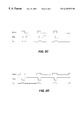
- FIGS. 2A, 2 B, 2 C and 2 D illustrate a source current, a sink current and output voltages of the charge pump circuit
- FIG. 3 illustrates charge pump output voltage vs. charge pump currents
- FIG. 4 is a schematic diagram of a charge pump circuit according to an embodiment of the present invention.
- FIG. 1 shows a prior art PLL including a phase/frequency comparator (PFC) 111 , a charge pump circuit 113 , a loop filter 115 , a voltage-controlled oscillator (VCO) 117 and a feedback divider (FBD) 119 having a frequency division ratio N.
- a reference signal of a frequency fr is fed to the PFC 111 .
- An output signal of the VCO 117 is fed to the FBD 119 which provides a frequency divided signal to the PFC 111 .
- the PFC 111 provides an input (an up signal UP or a down signal DN) to a charge pump circuit 113 .
- the charge pump circuit 113 translates the PFC output pulses to current pulses that are fed to the filter 115 .
- An output signal of the filter 115 drives the VCO 117 .
- a negative feedback exists in the loop. The negative feedback adjusts the VCO frequency of, so that the two input signals to the PFC 111 have the same frequency and phase, and the PLL is “locked”.
- the charge pump circuit 113 operates as a current source of current Iso and a current sink of current Isi, in response to the up signal UP and the down signal DN, respectively.
- the source and sink currents will be perfectly matched, as shown in FIG. 2 A.
- Such ideal source and sink current pulses result in a spur-free synthesized output from the VCO 117 .
- the PLL negative feedback adjusts the turn-on times of the sink and source currents with respect to each other, so that the average charge pump output voltage remains constant. If a leakage path to ground exists, the source and sink currents and the VCO control voltage are shown in FIG. 2 B. The source and sink current pulses must terminate simultaneously. If a time difference exists between the termination time of the source and sink currents, the PLL feedback enforces a time difference in the initialization of the two currents to keep the average VCO input voltage constant. The source and sink current pulses and the VCO control voltage for such a condition are shown in FIG. 2 C.
- the source and sink currents should have identical amplitudes. If there is a mismatch, the PLL feedback causes a mismatch in the initiation time of the two currents to keep the average VCO control voltage constant.
- Typical source and sink currents and the VCO control voltage for a PLL with a sink/source mismatch are shown in FIG. 2 D.
- any of the previously mentioned imperfections, or a combination of them causes an ac component with a frequency of fr to appear at the output of the charge pump circuit 113 .
- the ac component frequency modulates the VCO.
- the bandwidth of the filter 115 can be reduced to attenuate the ac component. However, this would have a negative effect on the switching speed of the PLL. Therefore, it is necessary to minimize the leakage and the timing and amplitude mismatch between the source and sink current pulses in a PLL charge pump circuit 113 .
- Any current source has a finite output impedance.
- the sink and source currents in a charge pump circuit are generated by current sources.
- the voltage across the sink current source is the charge pump output voltage.
- the source voltage is the supply voltage minus the charge pump voltage.
- the voltage at the output of the charge pump depends on the synthesized VCO output frequency. Typical sink and source current levels, as functions of the charge pump output voltage, are shown in FIG. 3 .
- the mismatch between the sink and source current amplitudes depends on the charge pump voltage.
- the reference feedthrough is worse for the charge pump voltages that are near 0 or the positive supply voltage.
- the charge pump voltage in general, can be any value between 0 and the supply voltage, only a portion of this range results in acceptable levels of reference feedthrough.
- the PLL operation must be limited to acquire a charge pump voltage away from the rails.
- the acceptable amount of reference feedthrough puts a limit on the range of voltage that can exist at the charge pump output. This puts a limit on the range of frequencies that can exit at the output of a given VCO. Therefore, it is required to maximize the voltage range at the charge pump output in which the mismatch is acceptable.
- Cascode FET current sources used in charge pump circuits provide higher output impedances.
- cascode current sources have a high compliance voltage. That cannot be tolerated in low-voltage applications (F. You et al, “An Improved Tail Current Source for Low Voltage Applications,” IEEE J. Solid-State Circuits, Vol. 32, No. 8, August 1997, pp. 1173-1180).
- MOSFETs metal oxide semiconductor field effect transistors
- FIG. 4 shows a charge pump circuit according to an embodiment of the present invention.
- the source-drain of a P-channel FET 211 , the drain-source of an N-channel FET 213 and a resistor 215 are connected in series between a terminal 217 of supply voltage Vdd (e.g., +3.3 volts) and the ground terminal.
- Vdd supply voltage
- the source-drain of a P-channel FET 219 , the drain-source of an N-channel FET 221 and a resistor 223 are connected in series between the terminal 217 and the ground terminal.
- the junction of the drains of the FETs 211 and 213 and the junction of the drains of the FETs 219 and 221 are connected to the non-inverting and inverting input terminals of a MOS operational amplifier 225 , the output terminal of which is connected to the gate of the FET 211 .
- the amplifier has an infinite input impedance.
- Two P-channel FETs 227 and 229 are connected in series between the terminal 217 and the gate of the FET 211 .
- the junction of the drain of the FET 227 and the source of the FET 229 is connected to the gate of the FET 219 .
- An inverter 231 is connected between a signal input terminal 233 and the gate of the FET 229 .
- the gate of the FET 227 is connected to the terminal 233 .
- the source of the FET 213 is connected to the inverting input terminal of a MOS operational amplifier 235 , the non-inverting input terminal of which is connected to a terminal 237 of reference voltage Vref.
- the reference voltage Vref is fed to the voltage terminal 237 by a dc supply (not shown).
- the amplifier 235 has an infinite input impedance.
- the output terminal of the amplifier 235 and the gate of the FET 213 are connected to the source of a P-channel FET 239 , the drain of which is connected to the drain of an N-channel FET 241 and the gate of the FET 221 .
- the source of the FET 241 is connected to the ground terminal.
- An inverter 243 is connected between a signal input terminal 245 and the gates of the FETs 239 and 241 . Pulse trains UP and DN are fed from a phase/frequency comparator (not shown) to the signal input terminals 233 and 245 , respectively.
- the junction of the drains of the FETs 219 and 221 is connected to an output terminal 247 which is connected to a loop filter 249 having a capacitor of an external circuit (e.g., a VCO of a PLL, not shown).
- the W/L (gate size) ratio of the P-channel FETs 211 and 219 is larger than that of the N-channel FETs 213 and 221 .
- the charge pump circuit further includes a start-up circuit of a comparator 311 and a FET 313 .
- the non-inverting input terminal of the amplifier 311 is connected to a voltage terminal 315 of a half reference voltage Vref/2.
- the inverting input terminal of the comparator 311 is connected to the inverting input terminal of the amplifier 235 .
- the output terminal of the comparator 311 is connected to the gate of the FET 313 , the source and drain of which are connected to the drain of the FET 229 and the ground terminal, respectively.
- Pulse trains UP and DN are fed from a phase/frequency comparator (not shown) to the signal input terminals 233 and 245 , respectively.
- the reference voltage Vref is fed to the voltage terminal 237 .
- the charge pump circuit sources current to and sinks current from the terminal 247 connected to the filter 249 and the VCO (not shown). A voltage is developed across the filter 249 .
- the pulse train UP is fed to the terminal 233 and no pulses DN are fed.
- the FETs 229 and 227 are on and off, respectively.
- the current Ipr is flowing in the series-connected FETs 211 and 213 .
- the voltage difference (Vn-Vc) is amplified by the amplifier 225 and its amplified output voltage Vgso is fed to the gate of the FET 219 via the on-FET 229 .
- current Iso flows in the FET 219 .
- the current Iso is mirrored current of the current Ipr.
- the current Iso is sourced to the filter 249 and charges the capacitor thereof.
- the amplifier 225 detects the voltage difference (Vn-Vc) in the current-source mode.
- the negative feedback provided by the amplifier 225 guarantees that the voltage Vn is equal to the voltage Vc.
- the drain-source voltage of the FET 211 is equal to that of the FET 219 .
- the current Iso flowing in the FET 219 is equal to the current Ipr flowing in the FET 211 .
- the pulse train DN is fed to the terminal 245 and no pulses UP are fed.
- the FETs 239 and 241 are on and off, respectively.
- the voltage Vgsi which is an amplified voltage of the voltage difference (Vref-Vs)
- Vref-Vs an amplified voltage of the voltage difference
- the current Isi flowing in the FET 221 in response to the voltage Vgsi is mirrored (i.e., multiplied) current of the current Ipr flowing in the FETs 211 and 213 .
- the current Isi is sunk from the filter 249 and discharges the capacitor thereof.
- the amplifier 235 detects the voltage difference (Vn-Vs) in the current-sink mode.
- the negative feedback provided by the amplifier 235 guarantees that the voltage Vn is equal to the voltage Vc.
- the drain-source voltage of the FET 213 is equal to that of the FET 221 .
- the current Isi flowing in the FET 221 is equal to the current flowing in the current Ipr flowing in the FET 213 .
- the negative feedback provided by the FETs 235 and 213 keeps the current of the FET 213 constant.
- the current of the FET 213 is independent from the drain-source voltage of the FET 213 .
- the current of the FET 211 is equal to that of the FET 213 and thus, the current of the FET 211 is also independent from the drain-source voltage of the FET 211 .
- the current Iso and Isi are X times (proportional) of the current Ipr.
- examples are:
- the voltages Vn and Vc are zero.
- the amplifier 225 may not turn on the FET 211 with a zero differential voltage at its inputs.
- the voltages Vn and Vc are zero, the voltage Vs across the resistor 215 is also zero.
- the output voltage of the comparator 311 is high, so that the FET 313 is turned on.
- the gate of the FET 211 is pulled to the ground potential and is turned on.
- the FET 213 is turned on by the output voltage of the amplifier 235 and current flows in the on-FETs 211 and 213 .
- the FET 219 sources current Iso to the output filter 249 , with the result that the output voltage Vc increases.
- the start-up circuit ensures that the charge pump circuit starts properly and achieves the normal operating conditions. Under the normal conditions, the voltage Vs across the resistor 215 is Vref and thus, the output voltage of the comparator 311 is low. The start-up circuit does not affect the operation of the charge pump circuit.
- FETs other than MOSFETs may be used and the FETs of a different channel type may be used.
- the FETs may be replaced by bipolar transistors.
Abstract
Description
Claims (14)
Priority Applications (1)
| Application Number | Priority Date | Filing Date | Title |
|---|---|---|---|
| US09/372,580 US6329872B1 (en) | 1998-08-14 | 1999-08-12 | Charge pump circuit for a phase locked loop |
Applications Claiming Priority (2)
| Application Number | Priority Date | Filing Date | Title |
|---|---|---|---|
| US9669298P | 1998-08-14 | 1998-08-14 | |
| US09/372,580 US6329872B1 (en) | 1998-08-14 | 1999-08-12 | Charge pump circuit for a phase locked loop |
Publications (1)
| Publication Number | Publication Date |
|---|---|
| US6329872B1 true US6329872B1 (en) | 2001-12-11 |
Family
ID=26791971
Family Applications (1)
| Application Number | Title | Priority Date | Filing Date |
|---|---|---|---|
| US09/372,580 Expired - Lifetime US6329872B1 (en) | 1998-08-14 | 1999-08-12 | Charge pump circuit for a phase locked loop |
Country Status (1)
| Country | Link |
|---|---|
| US (1) | US6329872B1 (en) |
Cited By (21)
| Publication number | Priority date | Publication date | Assignee | Title |
|---|---|---|---|---|
| US6509770B2 (en) * | 1999-08-18 | 2003-01-21 | Infineon Technologies Ag | Charge pump and PLL |
| US6667640B2 (en) * | 2001-10-23 | 2003-12-23 | Fujitsu Limited | Phase locked loop circuit having a wide oscillation frequency range for reducing jitter |
| US20040071252A1 (en) * | 2002-10-10 | 2004-04-15 | International Business Machines Corporation | Charge pump with transient current correction |
| US20040085106A1 (en) * | 2002-08-26 | 2004-05-06 | Integrant Technologies Inc. | Charge pump circuit for compensating mismatch of output currents |
| US20040132722A1 (en) * | 2000-10-17 | 2004-07-08 | The Procter & Gamble Company | Substituted heterocyclic compounds for treating multidrug resistance |
| US20050156640A1 (en) * | 2004-01-16 | 2005-07-21 | International Business Machines Corporation | Novel charge leakage correction circuit for applications in PLLs |
| US20050195003A1 (en) * | 2004-03-05 | 2005-09-08 | Soe Zaw M. | Charge pump circuit using active feedback controlled current sources |
| US7009432B2 (en) * | 2001-12-20 | 2006-03-07 | Analog Devices, Inc. | Self-calibrating phase locked loop charge pump system and method |
| US20060226917A1 (en) * | 2005-04-11 | 2006-10-12 | Sangbeom Park | High-performance charge-pump circuit for phase-locked loops |
| US20090033407A1 (en) * | 2007-08-03 | 2009-02-05 | Wyatt Stephen D | Structure for a high output resistance, wide swing charge pump |
| US20090033383A1 (en) * | 2007-08-03 | 2009-02-05 | Wyatt Stephen D | High output resistance, wide swing charge pump |
| US20100069016A1 (en) * | 2006-12-14 | 2010-03-18 | Mstar Semiconductor, Inc. | Noise Based Quality Estimation for Signals |
| US7701271B1 (en) | 2007-09-24 | 2010-04-20 | Ozmo, Inc. | High linearity charge pump method and apparatus |
| US7915933B2 (en) | 2006-11-30 | 2011-03-29 | Mosaid Technologies Incorporated | Circuit for clamping current in a charge pump |
| US20120025897A1 (en) * | 2010-07-30 | 2012-02-02 | Toyota Jidosha Kabushiki Kaisha | Drive unit for driving voltage-driven element |
| US8120405B1 (en) * | 2004-01-27 | 2012-02-21 | Integrated Device Technology, Inc. | Method and apparatus for an output buffer with dynamic impedance control |
| US20120300606A1 (en) * | 2011-05-27 | 2012-11-29 | Texas Instruments Incorporated | Current Driver Damping Circuit |
| US20130027086A1 (en) * | 2011-07-26 | 2013-01-31 | United Microelectronics Corp. | Charge pump |
| US20150091625A1 (en) * | 2013-09-30 | 2015-04-02 | Chengming He | High speed, low power, isolated buffer |
| US20190115829A1 (en) * | 2017-10-13 | 2019-04-18 | Qualcomm Incorporated | Power-up sequencing and high voltage protection for charge pump converters |
| USRE47715E1 (en) | 2003-12-11 | 2019-11-05 | Conversant Intellectual Property Management Inc. | Charge pump for PLL/DLL |
Citations (10)
| Publication number | Priority date | Publication date | Assignee | Title |
|---|---|---|---|---|
| US4814726A (en) | 1987-08-17 | 1989-03-21 | National Semiconductor Corporation | Digital phase comparator/charge pump with zero deadband and minimum offset |
| US5220294A (en) * | 1990-05-21 | 1993-06-15 | Nec Corporation | Phase-locked loop circuit |
| US5334951A (en) * | 1993-02-18 | 1994-08-02 | Northern Telecom Limited | Phase lock loops and methods for their operation |
| US5420545A (en) | 1993-03-10 | 1995-05-30 | National Semiconductor Corporation | Phase lock loop with selectable frequency switching time |
| EP0641082B1 (en) | 1993-08-23 | 1997-06-18 | Nec Corporation | PLL frequency synthesizer and PLL frequency synthesizing method capable of obtaining high-speed lock-up and highly-reliable oscillation |
| US5675291A (en) | 1996-02-16 | 1997-10-07 | National Semiconductor Corporation | Phase-lock loop with reduced acquistion time |
| EP0440405B1 (en) | 1990-01-29 | 1998-10-14 | Kabushiki Kaisha Toshiba | Channel selecting circuit |
| US5886551A (en) * | 1996-03-28 | 1999-03-23 | Nec Corporation | Charge pump circuit for use in a phase locked loop |
| US5945855A (en) * | 1997-08-29 | 1999-08-31 | Adaptec, Inc. | High speed phase lock loop having high precision charge pump with error cancellation |
| US6107889A (en) * | 1997-11-07 | 2000-08-22 | Analog Devices, Inc. | Phase locked loop charge pump circuit |
-
1999
- 1999-08-12 US US09/372,580 patent/US6329872B1/en not_active Expired - Lifetime
Patent Citations (10)
| Publication number | Priority date | Publication date | Assignee | Title |
|---|---|---|---|---|
| US4814726A (en) | 1987-08-17 | 1989-03-21 | National Semiconductor Corporation | Digital phase comparator/charge pump with zero deadband and minimum offset |
| EP0440405B1 (en) | 1990-01-29 | 1998-10-14 | Kabushiki Kaisha Toshiba | Channel selecting circuit |
| US5220294A (en) * | 1990-05-21 | 1993-06-15 | Nec Corporation | Phase-locked loop circuit |
| US5334951A (en) * | 1993-02-18 | 1994-08-02 | Northern Telecom Limited | Phase lock loops and methods for their operation |
| US5420545A (en) | 1993-03-10 | 1995-05-30 | National Semiconductor Corporation | Phase lock loop with selectable frequency switching time |
| EP0641082B1 (en) | 1993-08-23 | 1997-06-18 | Nec Corporation | PLL frequency synthesizer and PLL frequency synthesizing method capable of obtaining high-speed lock-up and highly-reliable oscillation |
| US5675291A (en) | 1996-02-16 | 1997-10-07 | National Semiconductor Corporation | Phase-lock loop with reduced acquistion time |
| US5886551A (en) * | 1996-03-28 | 1999-03-23 | Nec Corporation | Charge pump circuit for use in a phase locked loop |
| US5945855A (en) * | 1997-08-29 | 1999-08-31 | Adaptec, Inc. | High speed phase lock loop having high precision charge pump with error cancellation |
| US6107889A (en) * | 1997-11-07 | 2000-08-22 | Analog Devices, Inc. | Phase locked loop charge pump circuit |
Non-Patent Citations (1)
| Title |
|---|
| "An Improved Tail Current Source for Low Voltage Applications", F. You et al., IEEE Journal of Solid-State Circuits, vol. 32, No. 8, Aug. 1997, pp. 1173-1180. |
Cited By (37)
| Publication number | Priority date | Publication date | Assignee | Title |
|---|---|---|---|---|
| US6509770B2 (en) * | 1999-08-18 | 2003-01-21 | Infineon Technologies Ag | Charge pump and PLL |
| US20040132722A1 (en) * | 2000-10-17 | 2004-07-08 | The Procter & Gamble Company | Substituted heterocyclic compounds for treating multidrug resistance |
| US6667640B2 (en) * | 2001-10-23 | 2003-12-23 | Fujitsu Limited | Phase locked loop circuit having a wide oscillation frequency range for reducing jitter |
| US7009432B2 (en) * | 2001-12-20 | 2006-03-07 | Analog Devices, Inc. | Self-calibrating phase locked loop charge pump system and method |
| US6989698B2 (en) * | 2002-08-26 | 2006-01-24 | Integrant Technologies Inc. | Charge pump circuit for compensating mismatch of output currents |
| US20040085106A1 (en) * | 2002-08-26 | 2004-05-06 | Integrant Technologies Inc. | Charge pump circuit for compensating mismatch of output currents |
| US20040071252A1 (en) * | 2002-10-10 | 2004-04-15 | International Business Machines Corporation | Charge pump with transient current correction |
| US7162001B2 (en) | 2002-10-10 | 2007-01-09 | International Business Machines Corporation | Charge pump with transient current correction |
| USRE47715E1 (en) | 2003-12-11 | 2019-11-05 | Conversant Intellectual Property Management Inc. | Charge pump for PLL/DLL |
| US20050156640A1 (en) * | 2004-01-16 | 2005-07-21 | International Business Machines Corporation | Novel charge leakage correction circuit for applications in PLLs |
| US6958636B2 (en) * | 2004-01-16 | 2005-10-25 | International Business Machines Corporation | Charge leakage correction circuit for applications in PLLs |
| US8120405B1 (en) * | 2004-01-27 | 2012-02-21 | Integrated Device Technology, Inc. | Method and apparatus for an output buffer with dynamic impedance control |
| US6980046B2 (en) * | 2004-03-05 | 2005-12-27 | Wionics Research | Charge pump circuit using active feedback controlled current sources |
| US20050195003A1 (en) * | 2004-03-05 | 2005-09-08 | Soe Zaw M. | Charge pump circuit using active feedback controlled current sources |
| US20060226917A1 (en) * | 2005-04-11 | 2006-10-12 | Sangbeom Park | High-performance charge-pump circuit for phase-locked loops |
| US7190231B2 (en) * | 2005-04-11 | 2007-03-13 | Ana Semiconductor | High-performance charge-pump circuit for phase-locked loops |
| US8860480B2 (en) | 2006-11-30 | 2014-10-14 | Conversant Intellectual Property Management Inc. | Circuit for clamping current in a charge pump |
| US8456208B2 (en) | 2006-11-30 | 2013-06-04 | Mosaid Technologies Incorporated | Circuit for clamping current in a charge pump |
| US8149032B2 (en) | 2006-11-30 | 2012-04-03 | Mosaid Technologies Incorporated | Circuit for clamping current in a charge pump |
| US7915933B2 (en) | 2006-11-30 | 2011-03-29 | Mosaid Technologies Incorporated | Circuit for clamping current in a charge pump |
| US20110204939A1 (en) * | 2006-11-30 | 2011-08-25 | Mosaid Technologies Incorporated | Circuit for Clamping Current in a Charge Pump |
| US20100069016A1 (en) * | 2006-12-14 | 2010-03-18 | Mstar Semiconductor, Inc. | Noise Based Quality Estimation for Signals |
| US7701270B2 (en) | 2007-08-03 | 2010-04-20 | International Business Machines Corporation | Structure for a high output resistance, wide swing charge pump |
| US20090033383A1 (en) * | 2007-08-03 | 2009-02-05 | Wyatt Stephen D | High output resistance, wide swing charge pump |
| US20090033407A1 (en) * | 2007-08-03 | 2009-02-05 | Wyatt Stephen D | Structure for a high output resistance, wide swing charge pump |
| US7583116B2 (en) | 2007-08-03 | 2009-09-01 | International Business Machines Corporation | High output resistance, wide swing charge pump |
| US7701271B1 (en) | 2007-09-24 | 2010-04-20 | Ozmo, Inc. | High linearity charge pump method and apparatus |
| US20120025897A1 (en) * | 2010-07-30 | 2012-02-02 | Toyota Jidosha Kabushiki Kaisha | Drive unit for driving voltage-driven element |
| US8410825B2 (en) * | 2010-07-30 | 2013-04-02 | Toyota Jidosha Kabushiki Kaisha | Drive unit for driving voltage-driven element |
| US20120300606A1 (en) * | 2011-05-27 | 2012-11-29 | Texas Instruments Incorporated | Current Driver Damping Circuit |
| US8841943B2 (en) * | 2011-05-27 | 2014-09-23 | Texas Instruments Incorporated | Current driver damping circuit |
| US20130027086A1 (en) * | 2011-07-26 | 2013-01-31 | United Microelectronics Corp. | Charge pump |
| US8427210B2 (en) * | 2011-07-26 | 2013-04-23 | United Microelectronics Corp. | Charge pump |
| US20150091625A1 (en) * | 2013-09-30 | 2015-04-02 | Chengming He | High speed, low power, isolated buffer |
| US10389343B2 (en) * | 2013-09-30 | 2019-08-20 | Integrated Device Technology, Inc. | High speed, low power, isolated buffer |
| US20190115829A1 (en) * | 2017-10-13 | 2019-04-18 | Qualcomm Incorporated | Power-up sequencing and high voltage protection for charge pump converters |
| US10734891B2 (en) * | 2017-10-13 | 2020-08-04 | Qualcomm Incorporated | Power-up sequencing and high voltage protection for charge pump converters |
Similar Documents
| Publication | Publication Date | Title |
|---|---|---|
| US6329872B1 (en) | Charge pump circuit for a phase locked loop | |
| USRE49018E1 (en) | Charge pump for PLL/DLL | |
| US5734279A (en) | Charge Pump Circuit | |
| US6586976B2 (en) | Charge pump circuit for improving switching characteristics and reducing leakage current and phase locked loop having the same | |
| US6466078B1 (en) | Reduced static phase error CMOS PLL charge pump | |
| US6316987B1 (en) | Low-power low-jitter variable delay timing circuit | |
| US6124741A (en) | Accurate PLL charge pump with matched up/down currents from Vds-compensated common-gate switches | |
| US5801578A (en) | Charge pump circuit with source-sink current steering | |
| KR100374631B1 (en) | Charge pump circuit | |
| US6445211B1 (en) | Circuit technique for improved current matching in charge pump PLLS | |
| US6466070B1 (en) | Low voltage charge pump | |
| JP3109560B2 (en) | Semiconductor integrated circuit using variation compensation technology | |
| US6107889A (en) | Phase locked loop charge pump circuit | |
| US6426614B1 (en) | Boot-strapped current switch | |
| US5831484A (en) | Differential charge pump for phase locked loop circuits | |
| US5880579A (en) | VCO supply voltage regulator for PLL | |
| US7453313B2 (en) | Charge pumping circuit | |
| EP0841753A2 (en) | Charge pump circuit | |
| US6407596B1 (en) | Apparatus and method for a clock period subdivider | |
| US7190231B2 (en) | High-performance charge-pump circuit for phase-locked loops | |
| US6198320B1 (en) | Differential charge pump and filter with common-mode voltage control | |
| US6958637B2 (en) | Spark current cancellation in charge pump of high speed phase lock loop circuit | |
| CA2203496A1 (en) | Charge pump circuit | |
| JPH11330929A (en) | Circuit and method for controlling switching speed of inverter | |
| JPH04138774A (en) | Synchronizing signal separation circuit |
Legal Events
| Date | Code | Title | Description |
|---|---|---|---|
| AS | Assignment |
Owner name: NORTEL NETWORKS CORPORATION, CANADA Free format text: CHANGE OF NAME;ASSIGNOR:NORTHERN TELECOM LIMITED;REEL/FRAME:010567/0001 Effective date: 19990429 |
|
| AS | Assignment |
Owner name: NORTEL NETWORKS LIMITED, CANADA Free format text: CHANGE OF NAME;ASSIGNOR:NORTEL NETWORKS CORPORATION;REEL/FRAME:011195/0706 Effective date: 20000830 Owner name: NORTEL NETWORKS LIMITED,CANADA Free format text: CHANGE OF NAME;ASSIGNOR:NORTEL NETWORKS CORPORATION;REEL/FRAME:011195/0706 Effective date: 20000830 |
|
| STCF | Information on status: patent grant |
Free format text: PATENTED CASE |
|
| FPAY | Fee payment |
Year of fee payment: 4 |
|
| REMI | Maintenance fee reminder mailed | ||
| FPAY | Fee payment |
Year of fee payment: 8 |
|
| AS | Assignment |
Owner name: CIENA LUXEMBOURG S.A.R.L.,LUXEMBOURG Free format text: ASSIGNMENT OF ASSIGNORS INTEREST;ASSIGNOR:NORTEL NETWORKS LIMITED;REEL/FRAME:024213/0653 Effective date: 20100319 Owner name: CIENA LUXEMBOURG S.A.R.L., LUXEMBOURG Free format text: ASSIGNMENT OF ASSIGNORS INTEREST;ASSIGNOR:NORTEL NETWORKS LIMITED;REEL/FRAME:024213/0653 Effective date: 20100319 |
|
| AS | Assignment |
Owner name: CIENA CORPORATION,MARYLAND Free format text: ASSIGNMENT OF ASSIGNORS INTEREST;ASSIGNOR:CIENA LUXEMBOURG S.A.R.L.;REEL/FRAME:024252/0060 Effective date: 20100319 Owner name: CIENA CORPORATION, MARYLAND Free format text: ASSIGNMENT OF ASSIGNORS INTEREST;ASSIGNOR:CIENA LUXEMBOURG S.A.R.L.;REEL/FRAME:024252/0060 Effective date: 20100319 |
|
| FPAY | Fee payment |
Year of fee payment: 12 |
|
| AS | Assignment |
Owner name: DEUTSCHE BANK AG NEW YORK BRANCH, NEW YORK Free format text: SECURITY INTEREST;ASSIGNOR:CIENA CORPORATION;REEL/FRAME:033329/0417 Effective date: 20140715 |
|
| AS | Assignment |
Owner name: BANK OF AMERICA, N.A., AS ADMINISTRATIVE AGENT, NO Free format text: PATENT SECURITY AGREEMENT;ASSIGNOR:CIENA CORPORATION;REEL/FRAME:033347/0260 Effective date: 20140715 |
|
| AS | Assignment |
Owner name: CIENA CORPORATION, MARYLAND Free format text: RELEASE BY SECURED PARTY;ASSIGNOR:DEUTSCHE BANK AG NEW YORK BRANCH;REEL/FRAME:050938/0389 Effective date: 20191028 |
|
| AS | Assignment |
Owner name: BANK OF AMERICA, N.A., AS COLLATERAL AGENT, ILLINO Free format text: PATENT SECURITY AGREEMENT;ASSIGNOR:CIENA CORPORATION;REEL/FRAME:050969/0001 Effective date: 20191028 |
|
| AS | Assignment |
Owner name: CIENA CORPORATION, MARYLAND Free format text: RELEASE BY SECURED PARTY;ASSIGNOR:BANK OF AMERICA, N.A.;REEL/FRAME:065630/0232 Effective date: 20231024 |