US6331897B1 - Image processing method and apparatus in which a table stores by a scan line unit memory addresses at each of which a function is stored for developing an image for one line into a memory - Google Patents
Image processing method and apparatus in which a table stores by a scan line unit memory addresses at each of which a function is stored for developing an image for one line into a memory Download PDFInfo
- Publication number
- US6331897B1 US6331897B1 US08/788,574 US78857497A US6331897B1 US 6331897 B1 US6331897 B1 US 6331897B1 US 78857497 A US78857497 A US 78857497A US 6331897 B1 US6331897 B1 US 6331897B1
- Authority
- US
- United States
- Prior art keywords
- paint
- flow advances
- memory
- flow
- advances
- Prior art date
- Legal status (The legal status is an assumption and is not a legal conclusion. Google has not performed a legal analysis and makes no representation as to the accuracy of the status listed.)
- Expired - Fee Related
Links
Images


Classifications
-
- G—PHYSICS
- G06—COMPUTING; CALCULATING OR COUNTING
- G06K—GRAPHICAL DATA READING; PRESENTATION OF DATA; RECORD CARRIERS; HANDLING RECORD CARRIERS
- G06K15/00—Arrangements for producing a permanent visual presentation of the output data, e.g. computer output printers
-
- G—PHYSICS
- G06—COMPUTING; CALCULATING OR COUNTING
- G06K—GRAPHICAL DATA READING; PRESENTATION OF DATA; RECORD CARRIERS; HANDLING RECORD CARRIERS
- G06K15/00—Arrangements for producing a permanent visual presentation of the output data, e.g. computer output printers
- G06K15/02—Arrangements for producing a permanent visual presentation of the output data, e.g. computer output printers using printers
- G06K15/18—Conditioning data for presenting it to the physical printing elements
- G06K15/1801—Input data handling means
- G06K15/1803—Receiving particular commands
- G06K15/1805—Receiving printer configuration commands
-
- G—PHYSICS
- G06—COMPUTING; CALCULATING OR COUNTING
- G06K—GRAPHICAL DATA READING; PRESENTATION OF DATA; RECORD CARRIERS; HANDLING RECORD CARRIERS
- G06K15/00—Arrangements for producing a permanent visual presentation of the output data, e.g. computer output printers
- G06K15/02—Arrangements for producing a permanent visual presentation of the output data, e.g. computer output printers using printers
- G06K15/18—Conditioning data for presenting it to the physical printing elements
- G06K15/1801—Input data handling means
- G06K15/1803—Receiving particular commands
- G06K15/1806—Receiving job control commands
- G06K15/1807—Receiving job control commands relating to the print image preparation
-
- G—PHYSICS
- G06—COMPUTING; CALCULATING OR COUNTING
- G06K—GRAPHICAL DATA READING; PRESENTATION OF DATA; RECORD CARRIERS; HANDLING RECORD CARRIERS
- G06K15/00—Arrangements for producing a permanent visual presentation of the output data, e.g. computer output printers
- G06K15/02—Arrangements for producing a permanent visual presentation of the output data, e.g. computer output printers using printers
- G06K15/18—Conditioning data for presenting it to the physical printing elements
- G06K15/1801—Input data handling means
- G06K15/1822—Analysing the received data before processing
-
- G—PHYSICS
- G06—COMPUTING; CALCULATING OR COUNTING
- G06K—GRAPHICAL DATA READING; PRESENTATION OF DATA; RECORD CARRIERS; HANDLING RECORD CARRIERS
- G06K15/00—Arrangements for producing a permanent visual presentation of the output data, e.g. computer output printers
- G06K15/02—Arrangements for producing a permanent visual presentation of the output data, e.g. computer output printers using printers
- G06K15/18—Conditioning data for presenting it to the physical printing elements
- G06K15/1827—Accessing generic data, e.g. fonts
- G06K15/1828—Accessing generic data, e.g. fonts characterized by the kind of storage accessed
Definitions
- the present invention relates to an image processing method and apparatus and, more particularly, to an image processing method and apparatus, which can color-output a character, figure, raster image, and the like on the basis of print data, a command, and the like sent from a host computer.
- FIG. 1 shows a coordinate system serving as a reference for, e.g., coordinate points designated when a figure or character is drawn using a PDL (Page Description Language) or a page description command (this coordinate system will be referred to as a user coordinate system hereinafter).
- PDL Page Description Language
- page description command this coordinate system will be referred to as a user coordinate system hereinafter.
- a hatched rectangular portion in FIG. 1 indicates an effective print area (a possible draw area in a print sheet).
- the length of the effective print area will be referred to as an effective print area height hereinafter, and the width will be referred to as an effective print area width hereinafter.
- the coordinate system shown in FIG. 1 is a two-dimensional x-y orthogonal coordinate system, and has an origin at the lower left corner of the effective print area, as shown in FIG. 1 .
- the coordinate unit of this coordinate system can be desirably set (e.g., 0.01 mm, ⁇ fraction (1/72) ⁇ inch, and the like).
- Description elements of the PDL for figure drawing and page description commands which are set based on the above-mentioned user coordinate system, are analyzed in an image processing apparatus in the order of reception, and are converted into information to be developed on a memory.
- FIG. 2 shows a coordinate system serving as a reference for creating the above-mentioned memory development information (this coordinate system will be referred to as a printer coordinate system hereinafter).
- the coordinate unit of this coordinate system is determined by the resolution of an image processing apparatus used (for example, when the resolution is 300 dpi, the coordinate unit is ⁇ fraction (1/300) ⁇ inch).
- a hatched rectangular portion in FIG. 2 is the same as the effective print area in FIG. 1 .
- This coordinate system is a two-dimensional x-y orthogonal coordinate system, and has an origin at the upper left corner of the effective print area.
- FIG. 3 shows a memory map in an internal RAM area of a conventional image processing apparatus for performing color recording on the basis of the PDL or the page description command.
- the RAM area is constituted by a system work memory, a vacant area, and page development memories (each corresponding to the size of the effective print area shown in FIG. 2) for Y (Yellow), M (Magenta), C (Cyan), and Bk (Black).
- the system work memory is used as a storage area for information (variables, and the like) used in internal control of the image processing apparatus, a fixed work area, and the like.
- the vacant area is used as an area for storing memory development information, a character cache memory, and the like.
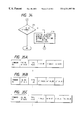
- FIG. 4 shows a paint color designation command of drawing attribute designation commands.
- This command is used for designating a color for painting a portion inside a closed figure.
- a command No. varies depending on drawing attribute designation, and is used for identifying command functions.
- the content of a number-of-data parameter indicates the number of data following the number-of-data parameter.
- the content of a number-of-data parameter of a line color designation command is 4.
- Y, M, C, and Bk values indicate density data values of Y (Yellow), M (Magenta), C (Cyan), and Bk (Black) as primary colors of coloring materials.
- FIG. 5 shows an example of a polygon drawing command of drawing commands.
- a command No. varies depending on drawing attribute designation, and is used for identifying command functions.
- the content of a number-of-data parameter indicates the number of data following the number-of-data parameter.
- X and Y values of coordinates 1 to n are coordinates on the user coordinate system.
- FIG. 6 shows an example of memory development information generated by analyzing the paint color designation command shown in FIG. 4 .
- a command table No. is used for identifying each memory development information.
- FIG. 7 shows an example of memory development information generated by analyzing the polygon drawing command shown in FIG. 5 .
- a command table No. is used for identifying each memory development information.
- the content of a number-of-data parameter indicates the number of data following the number-of-data parameter.
- X 1 , Y 1 , . . . , Xn, and Yn are coordinates converted into those on the printer coordinate system on the basis of the resolution of the image processing apparatus.
- FIG. 8 shows a case wherein drawing of a polygon defined by four coordinates (100, 200), (200, 200), (200, 100), and (100, 100) is set on the user coordinate system shown in FIG. 1 to have a coordinate unit of 1 mm.
- FIG. 9 shows an example of a command issued when the polygon drawing shown in FIG. 8 is set.
- FIG. 10 shows a case wherein polygon drawing on the user coordinate system shown in FIG. 8 is converted into polygon drawing on the printer coordinate system having a coordinate unit of ⁇ fraction (1/300) ⁇ inch (about ⁇ fraction (1/11.8) ⁇ mm).
- the effective print area height in this case is set to be 400 mm.
- the four coordinates are (1,180, 2,360), (2,360, 2,360), (2,360, 3,540), and (1,180, 3,540).
- FIG. 11 shows an example of memory development information of polygon drawing shown in FIG. 10, which information is generated by analyzing the polygon drawing command shown in FIG. 9 .
- FIG. 12 shows an example of memory development information set for paint color designation shown in FIG. 6 .
- each of Y, M, C, and Bk values ranges from 0 to 255.
- the Y value is set to be 255, and other values are set to be 0.
- FIG. 13 shows an example of memory development information set for paint color designation shown in FIG. 6 in a monochrome mode.
- a gray scale process using the coloring material Bk is performed in place of a color process using Y, M, C, and Bk.
- the gray scale density value ranges from 0 to 255.
- a value “51” indicates a density “20” [(51/255)%].
- FIG. 14 shows a state wherein the polygon shown in FIG. 10 is divided using the coordinate unit of the printer coordinate system.
- the minimum value of the Y-coordinate of this polygon is Y PMIN
- the maximum value of the Y-coordinate is Y PMAX .
- a paint pattern is developed on a development memory corresponding to a value between LEFTX and RIGHTX shown in FIG. 14 .
- FIG. 15 is a flow chart showing an example of a process for painting a portion inside the polygon shown in FIG. 14 .
- a drawing logic for the development memory of this example is “overwrite”.
- step S 300 it is checked if a color mode is selected.
- step S 300 If YES in step S 300 , the flow advances to step S 301 , and a paint process in the color mode is performed, thus ending the process.
- step S 300 If NO in step S 300 , the flow advances to step S 302 , and a paint process in the monochrome mode is performed, thus ending the process.
- FIGS. 16 to 21 are flow charts showing a summary of the paint process in the color mode in step S 301 in FIG. 15 .
- step S 310 memory development information for paint color designation shown in FIG. 6 is taken, and the flow advances to step S 311 .
- step S 311 Y, M, C, and Bk values of paint colors are taken from the taken memory development information for paint color designation, and are respectively set in P_Y, P_M, P_C, and P_Bk. Thereafter, the flow advances to step S 312 .
- step S 312 Y PMIN in FIG. 14 is set in ⁇ , and the flow advances to step S 313 .
- step S 313 LEFTX and RIGHTX defining a range of X to be painted are computed, and the flow advances to step S 314 .
- step S 314 addresses and bits on a Y-page memory in FIG. 3 corresponding to LEFTX and RIGHTX are computed, and the flow advances to step S 315 .
- step S 315 the address and bit corresponding to LEFTX computed in step S 314 are respectively set in Y LAD and Y LBIT , and the address and bit corresponding to RIGHTX are respectively set in Y RAD and Y RBIT . Thereafter, the flow advances to step S 316 .
- step S 316 P_Y is compared with 0.
- step S 316 If it is determined in step S 316 that P_Y ⁇ 0, the flow advances to step S 318 , and the storage address of a dither pattern corresponding to the value P_Y is taken. The flow then advances to step S 319 .
- step S 319 the dither pattern is taken from the storage address, and the flow advances to step S 320 .
- step S 320 the dither pattern taken in step S 318 is developed on the memory area (Y LAD , Y LBIT , Y RAD , Y RBIT ), and the flow advances to step S 321 .
- step S 321 the addresses and bits on an M-page memory in FIG. 3 corresponding to LEFTX and RIGHTX are computed, and the flow advances to step S 322 .
- step S 322 the address and bit corresponding to LEFTX computed in step S 321 are respectively set in M LAD and M LBIT , and the address and bit corresponding to RIGHTX are respectively set in M RAD and M RBIT . Thereafter, the flow advances to step S 323 .
- step S 323 P_M is compared with 0.
- step S 323 If it is determined in step S 323 that P_M ⁇ 0, the flow advances to step S 325 , and the storage address of a dither pattern corresponding to the value P_M is taken. Thereafter, the flow advances to step S 326 .
- step S 326 the dither pattern is taken from the storage address, and the flow advances to step S 327 .
- step S 327 the dither pattern taken in step S 326 is developed on the memory area (M LAD , M LBIT , M RAD , M RBIT ), and the flow advances to step S 328 .
- step S 328 the addresses and bits on a C-page memory in FIG. 3 corresponding to LEFTX and RIGHTX are computed, and the flow advances to step S 329 .
- step S 329 the address and bit corresponding to LEFTX computed in step S 328 are respectively set in C LAD and C LBIT , and the address and bit corresponding to RIGHTX are respectively set in C RAD and C RBIT . Thereafter, the flow advances to step S 330 .
- step S 330 P_C is compared with 0.
- step S 330 If it is determined in step S 330 that P_C ⁇ 0, the flow advances to step S 332 to take the storage address of a dither pattern corresponding to the value P_C, and the flow advances to step S 333 .
- step S 333 the dither pattern is taken from the storage address, and the flow advances to step S 334 .
- step S 334 the dither pattern taken in step S 333 is developed on the memory area (C LAD , C LBIT , C RAD , C RBIT ), and the flow advances to step S 335 .
- step S 335 the addresses and bits on a Bk-page memory in FIG. 3 corresponding to LEFTX and RIGHTX are computed, and the flow advances to step S 336 .
- step S 336 the address and bit corresponding to LEFTX computed in step S 335 are respectively set in K LAD and K LBIT , and the address and bit corresponding to RIGHTX are respectively set in K RAD and K RBIT .
- the flow then advances to step S 337 .
- step S 337 P_Bk is compared with 0.
- step S 337 If it is determined in step S 337 that P_Bk ⁇ 0, the flow advances to step S 339 to take the storage address of a dither pattern corresponding to the value P_Bk, and the flow advances to step S 340 .
- step S 340 the dither pattern is taken from the storage address, and the flow advances to step S 341 .
- step S 341 the dither pattern taken in step S 340 is developed on the memory area (K LAD , K LBIT , K RAD , K RBIT ), and the flow advances to step S 342 .
- step S 342 If it is determined in step S 342 that ⁇ Y PMAX , the flow advances to step S 343 to increment ⁇ by one, and the flow returns to step S 313 .
- FIGS. 22 and 23 are flow charts showing a summary of the paint process in the monochrome mode in step S 302 in FIG. 15 .
- step S 350 memory development information for paint color designation shown in FIG. 13 is taken, and the flow advances to step S 351 .
- step S 351 a gray scale density value of a paint color is taken from the taken memory development information for paint color designation, and is set in P_G. The flow then advances to step S 352 .
- step S 352 ⁇ is set in Y PMIN in FIG. 14, and the flow advances to step S 353 .
- step S 353 the storage address of a dither pattern corresponding to the value P_G is taken, and the flow advances to step S 354 .
- step S 354 the dither pattern is taken from the storage address, and the flow advances to step S 355 .
- step S 355 LEFTX and RIGHTX as a range of X to be painted are computed, and the flow advances to step S 356 .
- step S 356 the addresses and bits on the Bk-page memory in FIG. 3 corresponding to LEFTX and RIGHTX are computed, and the flow advances to step S 357 .
- step S 357 the address and bit corresponding to LEFTX computed in step S 356 are respectively set in K LAD and K LBIT , and the address and bit corresponding to RIGHTX are respectively set in K RAD and K RBIT .
- the flow then advances to step S 358 .
- step S 358 the dither pattern taken in step S 354 is developed on a memory area (K LAD , K LBIT , K RAD , K RBIT ), and the flow advances to step S 359 .
- step S 359 If it is determined in step S 359 that ⁇ Y PMAX , the flow advances to step S 360 to increment ⁇ by one, and the flow returns to step S 353 .
- a drawing pattern of each of Y (Yellow), M (Magenta), C (Cyan), and Bk (Black) as coloring materials of toners or inks is developed based on memory development information obtained by analyzing commands on a development memory having a size corresponding to the effective print area of a print sheet.
- a portion inside the polygon shown in FIG. 14 is painted by the processes shown in FIGS. 15 to 23 .
- each of the Y, M, C, and Bk density values is detected, and the paint process of a figure drawing on each of the Y-, M-, C-, and Bk-page memories is controlled based on the detected value, resulting in a long drawing time.
- each of Y, M, C, and Bk dither patterns corresponding to the Y, M, C, and Bk density values is taken from the storage area, and the paint process of a figure drawing on each page memory is controlled, resulting in a long drawing time.
- paint process efficiency e.g., a figure for bit map memories in units of coloring materials, i.e., Y, M, C, and Bk
- the present invention has a table for storing addresses of functions for developing a drawing such as a figure, a character, and the like in units of scan lines with respect to bit map memories in units of coloring materials or elements, and performs a development process using this table. Therefore, computation control need not be performed in units of scan lines, and the process time can be shortened.
- the storage address of a binary pattern, corresponding to the density value of each coloring material or element, of data to be developed on bit map memories in units of coloring materials or elements, is computed and stored.
- a binary pattern used when the data is developed on the bit map memory can be easily obtained, and the drawing time can be shortened.
- a plurality of tables each for storing addresses of functions for developing a drawing such as a figure, a character, and the like are prepared in correspondence with the number of designatable drawing logics.
- programs or hardware arrangements corresponding to the drawing logics need not be prepared.
- a table for storing addresses of functions for developing a drawing such as a figure, a character, and the like is set in correspondence with both the color output mode and the gray scale mode.
- programs or hardware arrangements in units of modes need not be prepared.
- FIG. 1 is a view of an example of a user coordinate system
- FIG. 2 is a view of an example of a printer coordinate system
- FIG. 3 is a view of an example of a memory map of a RAM area in a color image processing apparatus when each of Y, M, C, and Bk has a memory area corresponding to the size of an effective print area of a print sheet;
- FIG. 4 is a view of an example of a paint color designation command of drawing attribute commands
- FIG. 5 is a view of an example of a polygon drawing command of drawing commands
- FIG. 6 is a view of an example of memory development information for paint color designation of those for drawing attribute functions
- FIG. 7 is a view of memory development information for polygon drawing of those for drawing attribute functions
- FIG. 8 is a view of an example of polygon drawing on the user coordinate system
- FIG. 9 is a view of an example of a polygon drawing command issued when polygon drawing shown in FIG. 8 is set;
- FIG. 10 is a view of an example of conversion of polygon drawing shown in FIG. 8 onto the printer coordinate system
- FIG. 11 is a view of an example of memory development information of polygon drawing shown in FIGS. 8 and 10;
- FIG. 14 is a view of the polygon shown in FIG. 10 divided in coordinate units of the printer coordinate system
- FIG. 15 is a flow chart showing an example of a process for painting a portion inside the polygon shown in FIG. 14;
- FIG. 16 is a flow chart showing a process in step S 301 in FIG. 15;
- FIG. 17 is a flow chart showing the process in step S 301 in FIG. 15;
- FIG. 18 is a flow chart showing the process in step S 301 in FIG. 15;
- FIG. 19 is a flow chart showing the process in step S 301 in FIG. 15;
- FIG. 20 is a flow chart showing the process in step S 301 in FIG. 15;
- FIG. 21 is a flow chart showing the process in step S 301 in FIG. 15;
- FIG. 22 is a flow chart showing a process in step S 302 in FIG. 15;
- FIG. 23 is a flow chart showing the process in step S 302 in FIG. 15;
- FIG. 24 is comprised of FIGS. 24A and 24B block diagrams showing a circuit arrangement of an image processing apparatus according to an embodiment of the present invention
- FIG. 25 is a perspective view showing the details of an arrangement around a head unit of an ink jet type image processing apparatus
- FIG. 26 is a view showing the details of a head unit 101 shown in FIG. 25;
- FIG. 27 is a view of an example of a band structure
- FIG. 28 is a view of an example when an effective print area of a print sheet is divided into eight bands each having a band height of 512 scan lines;
- FIG. 29 is a view of an example of a memory map of a RAM area in a color mode
- FIG. 30 is a view of an example of a memory map of a RAM area in a monochrome mode
- FIG. 31 is a view of an example of an attribute information storage area for storing drawing attribute information used when data is developed on a memory
- FIG. 32 is a flow chart when color recording is performed using a memory for one band for each of Y (Yellow), M (Magenta), C (Cyan), and Bk (Black) in a color image processing apparatus for receiving page description command data in units of pages, and performing recording control in units of pages;
- FIG. 33 is a flow chart when color recording is performed using a memory for one band for each of Y (Yellow), M (Magenta), C (Cyan), and Bk (Black) in a color image processing apparatus for receiving page description command data in units of pages, and performing recording control in units of pages;
- FIG. 34 is a flow chart when color recording is performed using a memory for one band for each of Y (Yellow), M (Magenta), C (Cyan), and Bk (Black) in a color image processing apparatus for receiving page description command data in units of pages, and performing recording control in units of pages;
- FIGS. 35A to 35 C are views of examples of a color designation command of drawing attribute designation commands
- FIGS. 36A to 36 D are views respectively showing examples of a line width designation command, a clip area designation command, a paint definition designation command, and a drawing logic designation command of drawing attribute designation commands;
- FIG. 37 is a view of an example of a straight line drawing command/polygon drawing command of drawing commands
- FIG. 38 is a view of an example of a character drawing command of drawing commands
- FIG. 39 shows a command analysis jump table 4 in FIGS. 24A and 24B, which stores jump addresses to functions for analyzing drawing commands and drawing attribute commands;
- FIG. 40 is a flow chart showing the details of a command data analysis process in step S 3 in FIG. 32;
- FIG. 41 is a flow chart showing the details of a process upon execution of a color designation command analysis function in step S 34 in FIG. 40;
- FIG. 42 is a flow chart showing the details of the process upon execution of the color designation command analysis function in step S 34 in FIG. 40;
- FIG. 43 is a flow chart showing the details of the process upon execution of the color designation command analysis function in step S 34 in FIG. 40;
- FIG. 44 is a flow chart showing the details of the process upon execution of the color designation command analysis function in step S 34 in FIG. 40;
- FIG. 45 is a flow chart showing the details of a process upon execution of a line width designation command analysis function in step S 34 in FIG. 40;
- FIG. 46 is a flow chart showing the details of a process upon execution of a clip area designation command analysis function in step S 34 in FIG. 40;
- FIG. 47 is a flow chart showing the details of a process upon execution of a paint definition designation command analysis function in step S 34 in FIG. 40;
- FIG. 48 is a flow chart showing the details of a process upon execution of a drawing logic definition designation command analysis function in step S 34 in FIG. 40;
- FIG. 49 is a flow chart showing the details of a process for setting MIN band No. and MAX band No. in a memory development information area in steps S 40 , S 60 , S 70 , S 80 , and S 100 in FIGS. 41, 45 , 46 , 47 , and 48 ;
- FIG. 50 is a diagram of an example of a color reproduction process shown in steps S 701 and S 705 in FIG. 43;
- FIG. 51 shows equations as an example of a color conversion process shown in step S 703 in FIG. 43 and step S 713 in FIG. 44;
- FIG. 52 shows an equation as an example of a color conversion process shown in step S 704 in FIG. 43 and step S 714 in FIG. 44;
- FIG. 53 is a flow chart showing an example of a color conversion process shown in steps S 711 and S 715 in FIG. 44;
- FIG. 54 is a flow chart showing a process upon execution of a straight line drawing command analysis function in step S 34 in FIG. 40;
- FIG. 55 is a flow chart showing the process upon execution of the straight line drawing command analysis function in step S 34 in FIG. 40;
- FIG. 56 is a flow chart showing the process upon execution of the straight line drawing command analysis function in step S 34 in FIG. 40;
- FIG. 58 is a flow chart showing the process upon execution of the polygon drawing command analysis function in step S 34 in FIG. 40;
- FIG. 59 is a flow chart showing the process upon execution of the polygon drawing command analysis function in step S 34 in FIG. 40;
- FIG. 60 is a flow chart showing a process for setting data in a work area, and setting X MIN , Y MIN , X MAX , and Y MAX in step S 600 in FIG. 54 and step S 120 in FIG. 57;
- FIG. 61 is a flow chart showing the process for setting data in a work area, and setting X MIN , Y MIN , X MAX , and Y MAX in step S 600 in FIG. 54 and step S 120 in FIG. 57;
- FIG. 62 is a flow chart showing the process for setting data in a work area, and setting X MIN , Y MIN , X MAX , and Y MAX in step S 600 in FIG. 54 and step S 120 in FIG. 57;
- FIG. 63 is a flow chart showing a process upon execution of a character drawing command analysis function in step S 34 in FIG. 40;
- FIG. 64 is a flow chart showing the process upon execution of the character drawing command analysis function in step S 34 in FIG. 40;
- FIG. 65 is a flow chart showing the process upon execution of the character drawing command analysis function in step S 34 in FIG. 40;
- FIG. 66 is a flow chart showing the process upon execution of the character drawing command analysis function in step S 34 in FIG. 40;
- FIG. 67 is a flow chart showing a computation process of a drawing range in step S 601 in FIG. 54 and step S 121 in FIG. 57;
- FIG. 68 is a view of a drawing range of a polygon designated by four points (x 1 , y 1 ) to (x 4 , y 4 );
- FIG. 69 is a flow chart showing a computation process of a character drawing range in step S 220 in FIG. 64;
- FIG. 70 is a view of a character drawing range
- FIG. 71 is a flow chart showing a clip check process of a drawing range in step S 602 in FIG. 54, step S 122 in FIG. 57, and step S 220 in FIG. 64;
- FIG. 72 is a flow chart showing the clip check process of a drawing range in step S 602 in FIG. 54, step S 122 in FIG. 57, and step S 220 in FIG. 64;
- FIG. 73 is a view showing a case wherein a clip area of a rectangular area surrounded by (C XMIN , C YMIN ) and (C XMAX , C YMAX ) is set in a drawing range of a rectangular area surrounded by (P XIN , P YMIN ) and (P XMAX , P YMAX );
- FIG. 74 is a flow chart showing a process for computing MIN band No. and MAX band No. in step S 604 in FIG. 55, step S 124 in FIG. 58, and step S 222 in FIG. 65;
- FIGS. 75A and 75B are views of examples of memory development information for color designation generated by analyzing the color designation command in FIGS. 35A to 35 C on the basis of the flow charts of FIGS. 41 to 44 , in which FIG. 75A shows an example in a color mode, and FIG. 75B shows an example in a monochrome mode;
- FIG. 76A is a view of an example of memory development information generated by analyzing the line width designation command in FIG. 36A on the basis of the flow chart of FIG. 45,
- FIG. 76B is a view of an example of memory development information generated by analyzing the clip area designation command in FIG. 36B on the basis of the flow chart of FIG. 46,
- FIG. 76C is a view of an example of memory development information generated by analyzing the paint definition designation command in FIG. 36C on the basis of the flow chart of FIG. 47, and
- FIG. 76D is a view of an example of memory development information generated by analyzing the drawing logic designation command in FIG. 36D on the basis of the flow chart of FIG. 48;
- FIG. 77A is a view of an example of memory development information generated by analyzing the straight line drawing command in FIG. 37 on the basis of the flow charts of FIGS. 54 to 56 , and
- FIG. 77B is a view of an example of memory development information generated by analyzing the polygon drawing command in FIG. 37 on the basis of the flow charts of FIGS. 57 to 59 ;
- FIG. 78 is a view of an example of memory development information generated by analyzing the character drawing command in FIG. 38 on the basis of the flow charts of FIGS. 63 to 66 ;
- FIG. 79 is a view showing a case wherein one page is divided into four bands, and drawing is performed using Y, M, C, and Bk band memories each having a size corresponding to one band, and some drawing attribute commands and some drawing commands shown in FIGS. 27 to 30 ;
- FIG. 80 is a view of memory development information used in drawing in FIG. 79;
- FIG. 81 is a view of memory development information used in drawing in FIG. 79;
- FIG. 82 is a view showing a case wherein one page is divided into four bands, and drawing is performed using Y, M, C, and Bk band memories each having a size corresponding to one band while setting clip area designation for a straight line drawing;
- FIG. 83 is a view of memory development information used in drawing in FIG. 82;
- FIG. 84 shows a command execution jump table 1 , which stores jump addresses to functions for practically performing pattern development of a drawing onto a memory, and jump addresses to functions for designating drawing attributes (setting attributes in internal variables, and the like);
- FIG. 85 shows a command execution jump table 2 in which all jump addresses to functions for performing pattern development of a drawing onto a memory are replaced with jump addresses to skip functions in FIG. 84;
- FIG. 86 is a flow chart showing the details of a process in step S 12 in FIG. 33;
- FIG. 87 is a flow chart showing the details of a process in step S 390 in FIG. 86;
- FIG. 90 is a flow chart showing the details of a process in step S 391 in FIG. 86;
- FIG. 93 is a flow chart showing a process upon execution of a line width designation function in step S 399 in FIG. 86;
- FIG. 94 is a flow chart showing a process upon execution of a line color designation function in step S 399 in FIG. 86;
- FIG. 95 is a flow chart showing a process upon execution of a paint color designation function in step S 399 in FIG. 86;
- FIG. 96 is a flow chart showing a process upon execution of a character color designation function in step S 399 in FIG. 86;
- FIG. 97 is a flow chart showing a process upon execution of a clip area designation function in step S 399 in FIG. 86;
- FIG. 98 is a flow chart showing a process upon execution of a paint definition designation function in step S 399 in FIG. 86;
- FIG. 99 is a flow chart showing a process upon execution of a drawing logic designation function in step S 399 in FIG. 86;
- FIG. 100 is a flow chart showing a process upon execution of a straight line drawing function in step S 399 in FIG. 86;
- FIG. 101 is a flow chart showing the process upon execution of the straight line drawing function in step S 399 in FIG. 86;
- FIG. 102 is a flow chart showing a process upon execution of a polygon drawing function in step S 399 in FIG. 86;
- FIG. 103 is a flow chart showing the process upon execution of the polygon drawing function in step S 399 in FIG. 86;
- FIG. 104 is a flow chart showing the process upon execution of the polygon drawing function in step S 399 in FIG. 86;
- FIG. 105 is a flow chart showing the process upon execution of the polygon drawing function in step S 399 in FIG. 86;
- FIG. 106 is a flow chart showing a process upon execution of a character drawing function in step S 399 in FIG. 86;
- FIG. 107 is a flow chart showing the process upon execution of the character drawing function in step S 399 in FIG. 86;
- FIG. 108 is a flow chart showing a process upon execution of a skip function in step S 399 in FIG. 86;
- FIG. 109 shows an example of a dither pattern address table 21 ;
- FIGS. 110A and 110B are views of examples of a dither pattern
- FIG. 111 is a flow chart showing a process in step S 474 in FIG. 100, step S 500 in FIG. 103, step S 506 in FIG. 104, and step S 527 in FIG. 107;
- FIG. 112 is a flow chart showing a process in step S 474 in FIG. 100, step S 500 in FIG. 103, step S 506 in FIG. 104, and step S 527 in FIG. 107;
- FIG. 115 shows an example of a drawing logic table address storage table 24 ;
- FIGS. 116A and 116B are views of examples of a BITSET flag
- FIG. 117 is a flow chart showing a process in step S 475 in FIG. 100, step S 501 in FIG. 103, step S 507 in FIG. 104, and step S 528 in FIG. 107;
- FIG. 118 is a flow chart showing the process in step S 475 in FIG. 100, step S 501 in FIG. 103, step S 507 in FIG. 104, and step S 528 in FIG. 107;
- FIG. 119 is a flow chart showing the process in step S 475 in FIG. 100, step S 501 in FIG. 103, step S 507 in FIG. 104, and step S 528 in FIG. 107;
- FIG. 120 is a view of an example of a straight line connecting two points on the printer coordinate system
- FIG. 121 is a flow chart showing a process in step S 479 in FIG. 101 and step S 511 in FIG. 105;
- FIG. 122 is a flow chart showing the process in step S 479 in FIG. 101 and step S 511 in FIG. 105;
- FIG. 123 is a flow chart showing the process in step S 479 in FIG. 101 and step S 511 in FIG. 105;
- FIG. 124 is a view of an example of a polygon defined by five points on the printer coordinate system
- FIG. 125 is a view of an example of a character “E” defined by 12 outline points on the printer coordinate system
- FIG. 126 is a flow chart showing a process in step S 502 in FIG. 103 and step S 529 in FIG. 107;
- FIG. 127 is a flow chart showing a process in step S 860 in FIG. 122 and step S 871 in FIG. 126;
- FIG. 128 is a flow chart showing the process in step S 860 in FIG. 122 and step S 871 in FIG. 126;
- FIG. 129 is a flow chart showing a process in step S 862 in FIG. 123 and step S 873 in FIG. 126;
- FIG. 130 is a flow chart showing the process in step S 862 in FIG. 123 and step S 873 in FIG. 126;
- FIG. 131 is a flow chart showing the process in step S 862 in FIG. 123 and step S 873 in FIG. 126;
- FIG. 132 is a flow chart showing the process in step S 862 in FIG. 123 and step S 873 in FIG. 126;
- FIG. 133 is a view showing information necessary for explaining drawing of the straight line shown in FIG. 120;
- FIG. 134 is a view showing information necessary for explaining a process for painting a portion inside the polygon in FIG. 124;
- FIG. 135 is a view showing information necessary for explaining a process for painting a portion inside the character in FIG. 125;
- FIG. 136 is a flow chart showing an example of a clear paint process in the process in step S 922 in FIG. 132;
- FIG. 137 is a flow chart showing an example of the clear paint process in the process in step S 922 in FIG. 132;
- FIG. 138 is a flow chart showing an example of an overwrite paint process of the process in step S 922 in FIG. 132;
- FIG. 139 is a flow chart showing an example of the overwrite paint process of the process in step S 922 in FIG. 132;
- FIG. 140 is a flow chart showing an example of a reverse paint process of the process in step S 922 in FIG. 132;
- FIG. 141 is a flow chart showing an example of the reverse paint process of the process in step S 922 in FIG. 132;
- FIG. 142 is a flow chart showing an example of a transparent paint process of the process in step S 922 in FIG. 132;
- FIG. 143 is a flow chart showing an example of the transparent paint process of the process in step S 922 in FIG. 132;
- FIG. 144 is a view showing an example of the paint processes shown in FIGS. 136 to 143 ;
- FIG. 145 is a view showing another embodiment of FIG. 133;
- FIGS. 146A and 146B are views showing other embodiments of FIGS. 116A and 116B.
- FIG. 147 is a view showing a polygon including two portions to be painted with respect to one scan line of a Y coordinate.
- FIG. 24 is comprised of FIGS. 24A and 25B block diagrams showing a circuit arrangement of an image processing apparatus according to an embodiment of the present invention.
- an image processing apparatus is constituted by a host computer 1 and an image processing apparatus main body 1000 .
- the host computer 1 supplies print data, a print command, and the like to the image processing apparatus, and causes the image processing apparatus to perform a recording process.
- the image processing apparatus has a microprocessor system including a CPU, a ROM, and a RAM. More specifically, the image processing apparatus main body comprises: an interface 2 for exchanging data with the host computer 1 ; a command analyzer 3 which includes a command analysis table 4 storing jump addresses to analysis programs corresponding to command Nos.
- a band information storage 5 which includes a band height information table 6 storing a band height and information (memory capacity) of a development memory for a corresponding coloring material, and which stores information of band heights, and the like; a color reproduction information storage 7 storing information required in a color reproduction process; a color reproduction processor 8 for performing the color reproduction process; a character information storage 9 storing information for drawing a character; a controller 10 for controlling the apparatus; a memory development information storage 11 including an attribute information storage area 12 for storing attribute information, and a memory development information storage area 13 for storing information to be developed on a memory; a memory development information analyzer 14 which includes a command execution jump table 1 (15) and a command execution jump table 2 (16), and analyzes memory development information; a pattern developer 17 for developing analyzed memory development information on a development memory 18 consisting of four
- FIG. 25 is a perspective view showing details of an arrangement around a head unit of an ink jet type image processing apparatus.
- Head units 101 consist of Y, M, C, and Bk head units each including a large number of ink jet heads arranged in the sub-scan direction for one coloring material.
- Ink tanks 102 for the head units 101 , and signal lines 103 are connected to the head units 101 .
- a carriage drive motor 104 moves a carriage, which mounts the head units, along a rail in cooperation with a conveyor belt.
- a recording sheet 107 fed from a recording sheet roll 111 is wound around a platen 108 via a guide roller 112 , and is fed by recording sheet convey rollers 109 and 110 .
- Each head unit 101 consists of a plurality of ink jet heads utilizing heat generation elements, as shown in FIG. 26 .
- ink jet heads using electro-mechanical conversion means such as piezo elements may be used instead.
- FIG. 26 shows the details of the head units 101 shown in FIG. 25 .
- each head unit has Y, M, C, or Bk nozzles corresponding in number to each head height.
- the head units 101 respectively have yellow ink ejection nozzles, magenta ink ejection nozzles, cyan ink ejection nozzles, and black ink ejection nozzles.
- FIG. 27 shows an example of a band structure.
- a rectangular area having an effective print area width of a print sheet as a horizontal length, and a head height as a vertical length is defined as a segment.
- One band is an area obtained by vertically arranging the segments, as shown in FIG. 27, and has a size corresponding to an integer multiple of the segment size.
- the band height (the height of the band) corresponds to an integer multiple of the head height.
- one band is constituted by four segments.
- FIG. 28 shows a case wherein the effective print area of a print sheet is divided into eight bands each having a band height of 512 scan lines.
- band Nos. 0 to 7 are assigned to the eight bands.
- the band No. ranges from 0 to (n ⁇ 1).
- Points such as (0, 512) on the printer coordinate system shown in FIG. 28 indicate points at the upper left corners of the bands, and are computed by (0, (n ⁇ 1) ⁇ 512).
- the effective print area height is not always equal to an integer multiple of the band height, and the height of the final band (band 7 in FIG. 28) may often become equal to or smaller than the band height.
- FIG. 29 shows an example of a memory map of an internal RAM area of the color image processing apparatus in a color mode.
- the RAM area in the color mode is constituted by a system work memory, a vacant area, and 1-band memories for Y (Yellow), M (Magenta), C (Cyan), and Bk (Black) as coloring materials (toners or inks) (memories each having a size corresponding to one band area in FIG. 28 ).
- FIG. 30 shows an example of a memory map of the internal RAM area of the color image processing apparatus in a monochrome mode.
- the RAM area in the monochrome mode is constituted by a system work memory, a vacant area, and a 1-band memory for Bk (Black) as a coloring material (toner or ink) (a memory having a size corresponding to one band area in FIG. 28 ).
- the 1-band memories for Y (Yellow), M (Magenta), and C (Cyan) can be effectively utilized as a vacant area.
- the system work memory is used as a storage area of information (e.g., variables) used in internal control of the image processing apparatus, a permanent work area, and the like.
- the vacant area is used as an area for storing memory development information, a character cache memory, and the like.
- FIG. 31 shows the attribute information storage area (RAM) 12 shown in FIGS. 24A and 24B.
- the attribute information storage area is constituted by areas for temporarily retreating drawing attribute information used upon development data onto a memory, and variable areas set with the drawing attribute information.
- retreat areas are determined in correspondence with drawing attributes, and m pieces of information can be retreated.
- L WIDTH , L YMCK , and the like represent variables in each of which the drawing attribute information is set.
- FIGS. 32, 33 , and 34 are flow charts for performing color recording using only the 1-band memories for Y (Yellow), M (Magenta), C (Cyan), and Bk (Black) in the color image processing apparatus for receiving page description command data in units of pages, and performing recording control in units of pages.
- step S 1 the attribute information storage area shown in FIG. 31 is assured on a RAM, and the flow advances to step S 2 .
- step S 2 a set of command data (a drawing command, a drawing attribute command, and the like) are read, and the flow advances to step S 3 .
- step S 3 the command analyzer 3 analyzes the command data, and the flow advances to step S 4 .
- step S 4 If it is determined in step S 4 that command data for one page remain, the flow returns to step S 2 ; otherwise, the flow advances to step S 5 .
- step S 5 drawing attribute information required for data development onto the memories at this time is temporarily retreated on the retreat area in the attribute information storage area 12 assured in step S 1 , and the flow advances to step S 10 .
- step S 10 “0” is set in a constant i, and the flow advances to step S 11 .
- step S 11 a pointer is placed at the head of the first set of memory development information stored in the memory development information area 13 , and the flow advances to step S 12 .
- step S 12 the memory development information read in step S 11 is analyzed by the memory development information analyzer 14 , and is developed on the development memories corresponding to a band i portion (i.e., the Y, M, C, and Bk band memories). Thereafter, the flow advances to step S 13 .
- a band i portion i.e., the Y, M, C, and Bk band memories.
- step S 13 If it is determined in step S 13 that memory development information remains, the flow advances to step S 14 , and the pointer is placed at the head of the next set of memory development information. The flow then returns to step S 12 .
- step S 13 If it is determined in step S 13 that no memory development information remains, the flow advances to step S 15 .
- step S 15 the contents of the memories developed in step S 12 are color-recorded by the output unit 19 , and the flow advances to step S 16 .
- step S 16 i is incremented by one, and the flow advances to step S 17 .
- step S 17 the Y, M, C, and Bk band memories are cleared, and the flow advances to step S 18 .
- step S 18 the number of bands is compared with i. If the number of bands is equal to i, the process ends.
- step S 19 the drawing attributes temporarily retreated in the retreat areas in the attribute information storage area 12 in step S 5 are loaded, and are set in the variable areas of the attribute information storage area 12 . Thereafter, the flow returns to step S 11 .
- color recording can be performed using only the 1-band memories for Y (Yellow), M (Magenta), C (Cyan), and Bk (Black).
- FIGS. 35A, 35 B, and 35 C show examples of color designation commands (line color designation, paint color designation, and character color designation) of the drawing attribute designation commands.
- a line color designation command is used for designating a color of a straight line or an outline of a figure.
- a paint color designation command is used for designating a color for painting a portion inside a closed figure.
- a character color designation command is used for designating a color of a character.
- a command No. varies depending on color designation commands, and is used for identifying a command.
- the content of a number-of-data parameter indicates the number of data following the number-of-data parameter.
- the content of a type flag parameter indicates the type of color designation data.
- CIE Commission Internationale de l'Eclairage
- FIGS. 36A to 36 D show examples of a line width designation command, a clip area designation command, a paint definition designation command, and a drawing logic designation command of the drawing attribute designation commands.
- a command No. varies depending on drawing attribute designation commands, and is used for identifying a command.
- the content of a number-of-data parameter indicates the number of data following the number-of-data parameter.
- a line width designation command shown in FIG. 36A is used for designating a line width of a straight line or an outline of a figure.
- the line width value also uses the coordinate unit of the user coordinate system as a unit.
- a clip area designation command shown in FIG. 36B is used for designating a drawable range of a figure, a character, or the like.
- X and Y MIN and MAX values use the coordinate unit of the user coordinate system as a unit.
- a paint definition designation command shown in FIG. 36C is used for designating a paint pattern inside an outline of a closed figure, and the presence/absence of an outline.
- a paint pattern No. is used for identifying a paint pattern.
- An outline flag indicates the absence of an outline when it is “0”, and indicates the presence of an outline when it is “1”.
- a drawing logic designation command shown in FIG. 36D is used for designating a drawing logic of a figure, a character, or the like, i.e., a drawing logic (overwrite, transparent, or the like) for a memory upon development of a pattern on a development memory.
- drawing logic when a drawing logic is “overwrite”, a drawing logic value “0” is designated; when a drawing logic is “transparent”, a drawing logic value “1” is designated.
- FIG. 37 shows an example of a straight line drawing command or a polygon drawing command of the drawing commands.
- a command No. varies depending on drawing functions, and is used for identifying a command.
- the content of a number-of-data parameter indicates the number of data following the number-of-data parameter.
- a straight line drawing command is used for drawing a straight line.
- a polygon drawing command is used for drawing a polygon.
- X and Y values in coordinates 1 to n are coordinate values on the user coordinate system.
- FIG. 38 shows an example of a character drawing command of the drawing commands.
- a command No. varies depending on drawing functions, and is used for identifying a command.
- the content of a number-of-data parameter indicates the number of data following the number-of-data parameter.
- a character drawing command is used for drawing a character.
- X and Y coordinates of a drawing position are coordinates on the user coordinate system, which indicate a start reference position of character drawing.
- Character data represents a character string (e.g., ABC) to be printed.
- FIG. 39 shows the command analysis jump table (ROM) 4 (FIGS. 24 A and 24 B), which stores jump addresses to functions for analyzing drawing commands and drawing attribute commands.
- ROM command analysis jump table
- the table 4 stores jump addresses to command analysis functions in correspondence with command Nos. (0 to n).
- FIG. 40 is a flow chart showing the details of the command data analysis process in step S 3 in FIG. 32 .
- step S 30 a command No. is taken out of a set of command data, and the flow advances to step S 31 .
- step S 31 a pointer is placed at the head of the command analysis jump table shown in FIG. 39, and the flow advances to step S 32 .
- step S 32 the pointer is advanced by an amount corresponding to the command No., and the flow advances to step S 33 .
- step S 33 the content (jump address) indicated by the pointer is taken, and the flow advances to step S 34 .
- step S 34 a function indicated by the taken jump address is executed, and the process ends.
- FIGS. 41 and 42 are flow charts showing the details of a process upon execution of a color designation command analysis function in step S 34 in FIG. 40 .
- step S 40 MIN and MAX band Nos. are set in the memory development information storage area 13 , and the flow advances to step S 41 .
- step S 41 a command No. is read from a command, and is set in the memory development information storage area 13 to advance a pointer. Thereafter, the flow advances to step S 42 .
- step S 42 the number of data is read from the command, and (the number of data ⁇ 1) is set in a constant n. The flow then advances to step S 43 .
- step S 43 “4” is set as the number of data in the memory development information storage area 13 to advance a pointer, and the flow advances to step S 44 .
- step S 44 a type parameter is read from the command and is set in a type flag C SMFLG .
- the flow then advances to step S 45 .
- step S 45 color designation data corresponding in number to the constant n are read, and the flow advances to step S 46 .
- step S 46 It is checked in step S 46 if the value of the type flag C SMFLG is one of 0, 1, and 2.
- step S 46 If NO in step S 46 , the process ends.
- step S 46 the flow advances to step S 47 to check if the color mode is set.
- step S 47 If YES in step S 47 , the flow advances to step S 48 to execute a color conversion process in the color mode, and the flow then advances to step S 50 .
- step S 47 the flow advances to step S 49 to execute a color conversion process in the monochrome mode, and the flow then advances to step S 50 .
- step S 50 Y, M, C, and Bk density data are set in the memory development information storage area 13 , and a pointer is advanced, thus ending the process.
- the color designation command is analyzed, and memory development information for color designation is generated.
- FIG. 43 is a flow chart showing the details of a process upon execution of the color conversion process in the color mode in step S 48 in FIG. 42 .
- step S 700 the value of the type flag C SMFLG is compared with 0.
- step S 702 the value of the type flag C SMFLG is compared with 1.
- CIE Commission Internationale de l'Eclairage
- step S 704 the CIE XYZ data are converted into R, G, and B brightness data, and the flow advances to step S 705 .
- step S 705 the R, G, and B brightness data are converted into Y, M, C, and Bk density data, and the process ends.
- step S 702 If it is determined in step S 702 that the type flag C SMFLG ⁇ 1, the process ends.
- color designation data are converted into Y, M, C, and Bk density data.
- FIG. 44 is a flow chart showing the details of a process upon execution of the color conversion process in the monochrome mode in step S 49 in FIG. 42 .
- step S 710 the value of the type flag C SMFLG is compared with 0.
- step S 711 since it indicates that color designation data read in step S 45 are R, G, and B brightness data, the flow advances to step S 711 , and the R, G, and B brightness data are converted into gray scale density data. The flow then advances to step S 716 .
- CIE Commission Internationale de l'Eclairage
- step S 714 the CIE XYZ data are converted into R, G, and B brightness data, and the flow advances to step S 715 .
- step S 715 the R, G, and B brightness data are converted into gray scale density data, and the flow advances to step S 716 .
- step S 716 gray scale density data Gray is set in Y density data, and 0 is set in M, C, and Bk density data, thus ending the process.
- gray scale density data, 0, 0, 0, are stored in a color information portion of the memory development information of the gray scale density data.
- color designation data are converted into gray scale density data.
- FIG. 45 is a flow chart showing the details of a process upon execution of a line width designation command analysis function in step S 34 in FIG. 40 .
- step S 60 MIN and MAX band Nos. are set in the memory development information storage area 13 , and the flow advances to step S 61 .
- step S 61 a command No. is read from a command, and is set in the memory development information storage area 13 to advance a pointer. The flow then advances to step S 62 .
- step S 62 the number of data is read from the command, and is set as the number of data in the memory development information storage area 13 to advance a pointer. The flow then advances to step S 63 .
- step S 63 a line value parameter is read from the command, and the flow advances to step S 64 .
- step S 64 the read line width value is converted into a pixel (dot) value on the basis of the resolution of the image processing apparatus, and the flow advances to step S 65 .
- step S 65 the converted line width value is set in an internal variable L WIDTH , and the flow advances to step S 66 .
- step S 66 the converted line width value is set in the memory development information storage area 13 to advance a pointer, and the process ends.
- FIG. 46 is a flow chart showing the details of a process upon execution of a clip area designation command analysis function in step S 34 in FIG. 40 .
- step S 70 MIN and MAX band Nos. are set in the memory development information storage area 13 , and the flow advances to step S 71 .
- step S 71 a command No. is read from a command, and is set in the memory development information storage area 13 to advance a pointer. The flow then advances to step S 72 .
- step S 72 the number of data is read from the command, and is set as the number of data in the memory development information storage area 13 to advance a pointer.
- the flow advances to step S 73 .
- step S 73 X and Y MIN and MAX value parameters of a clip area are read from the command, and the flow advances to step S 74 .
- step S 74 the read X and Y MIN and MAX values are converted into values X MIN , Y MIN , X MAX and Y MAX on the printer coordinate system on the basis of the resolution of the image processing apparatus, and the flow advances to step S 75 .
- step S 75 the values X MIN , Y MIN , X MAX , and Y MAX are respectively set in C XMIN , C YMIN , C XMAX , and C YMAX , and the flow advances to step S 76 .
- step S 76 the value s X MIN , Y MIN , X MAX , and Y MAX are set in the memory development information storage area 13 to advance a pointer, and the process ends.
- the clip area designation command is analyzed, and memory development information for clip area designation is generated.
- FIG. 47 is a flow chart showing the details of a process upon execution of a paint definition designation command analysis function in step S 34 in FIG. 40 .
- step S 80 MIN and MAX band Nos. are set in the memory development information storage area 13 , and the flow advances to step S 81 .
- step S 81 a command No. is read from a command, and is set in the memory development information storage area 13 to advance a pointer. The flow then advances to step S 82 .
- step S 82 the number of data is read from the command, and is set as the number of data in the memory development information storage area 13 to advance a pointer. The flow then advances to step S 83 .
- step S 83 a paint pattern No. is read from the command, and is set in the memory development information storage area 13 to advance a pointer. The flow then advances to step S 84 .
- step S 84 an outline flag is read from the command, and is set in the memory development information storage area 13 to advance a pointer. The flow then advances to step S 85 .
- step S 85 the paint pattern No. is set in an internal variable F PAT , and the flow advances to step S 86 .
- step S 86 the content of the outline flag is set in an internal variable F PERMT , and the process ends.
- the paint definition designation command is analyzed, and memory development information for paint definition designation is generated.
- FIG. 48 is a flow chart showing the details of a process upon execution of a drawing logic designation command analysis function in step S 34 in FIG. 40 .
- step S 100 MIN and MAX band Nos. are set in the memory development information storage area 13 , and the flow advances to step S 101 .
- step S 101 a command No. is read from a command, and is set in the memory development information storage area 13 to advance a pointer. The flow then advances to step S 102 .
- step S 102 the number of data is read from the command, and is set as the number of data in the memory development information storage area 13 to advance a pointer. The flow then advances to step S 103 .
- step S 103 a drawing logic parameter is read from the command, and the flow advances to step S 104 .
- step S 104 the drawing logic is set in the memory development information storage area 13 to advance a pointer, and the process ends.
- drawing logic designation command is analyzed, and memory development information for drawing logic designation is generated.
- FIG. 49 is a flow chart showing the details of the process for setting the MIN and MAX band Nos. in the memory development information storage area in steps S 40 , S 60 , S 70 , S 80 , and S 100 in FIGS. 41 to 48 .
- step S 90 “0” is set in the MIN band No., and the flow advances to step S 91 .
- FIG. 50 is a diagram showing an example of a color reproduction process in steps S 701 and S 705 in FIG. 43 .
- process 3 a masking process for correcting unnecessary absorption characteristics of C, M, and Y toners or inks to achieve proper color reproduction is performed.
- a ⁇ conversion process is performed so as to adjust the contrast and brightness in correspondence with an image.
- CIE L*, a*, and b* data can be converted into CIE XYZ data by equations (a) to (d).
- step S 720 an R brightness data value is multiplied with 0.289659, and the product is set in R′. The flow then advances to step S 721 .
- step S 723 a sum of R′+G′+B′ is set in gray, and the flow advances to step S 724 .
- step S 600 data is set in a work area, and X MIN , Y MIN , X MAX , and Y MAX are set.
- the flow advances to step S 601 .
- step S 601 a drawing range is computed (straight line and polygon), and the flow advances to step S 602 .
- step S 602 a clip check process of a drawing range is performed, and the flow advances to step S 603 .
- step S 606 the MIN and MAX band Nos. are set in the memory development information storage area 13 to advance pointer 1 , and the flow advances to step S 607 .
- step S 607 pointer 2 is placed at the first position of a work area, and the flow advances to step S 608 .
- step S 609 pointer 1 and pointer 2 are advanced, and the flow advances to step S 610 .
- step S 611 “1” is set in m, and the flow advances to step S 612 .
- step S 612 X m and Y m are taken out of the work area, and are set in the memory development information storage area 13 . The flow then advances to step S 613 .
- step S 613 m and n (the number of coordinates) are compared with each other.
- step S 614 If n>m, the flow advances to step S 614 , and m is incremented by 1. The flow then advances to step S 615 .
- step S 615 pointer 1 and pointer 2 are advanced, and the flow returns to step S 612 .
- FIGS. 57 to 59 are flow charts showing a process upon execution of a polygon drawing command analysis function in step S 34 in FIG. 40 .
- step S 120 data is set in a work area, and X MIN , Y MIN , X MAX , and Y MAX are set.
- the flow advances to step S 121 .
- step S 121 a drawing range is computed (straight line and polygon), and the flow advances to step S 122 .
- step S 122 a clip check process of the drawing range is performed, and the flow advances to step S 123 .
- step S 123 a drawing range flag set in the clip check process of the drawing range is checked.
- step S 124 If the drawing range flag is not ERROR, the flow advances to step S 124 to compute MIN and MAX band Nos., and the flow advances to step S 125 .
- step S 125 pointer 1 is placed in the memory development information storage area 13 , and the flow advances to step S 126 .
- step S 126 the MIN and MAX band Nos. are set in the memory development information storage area 13 to advance pointer 1 , and the flow advances to step S 127 .
- step S 127 pointer 2 is placed at the first position of the work area, and the flow advances to step S 128 .
- step S 128 a command No. is taken out of the work area, and is set in the memory development information storage area 13 . Thereafter, the flow advances to step S 129 .
- step S 129 pointer 1 and pointer 2 are advanced, and the flow advances to step S 130 .
- step S 130 the number of data is taken out of the work area, and (the number of data+2) is set in the memory development information storage area 13 . The flow then advances to step S 131 .
- step S 131 “1” is set in m, and the flow advances to step S 132 .
- step S 132 X m and Y m are taken out of the work area, and are set in the memory development information storage area 13 . The flow then advances to step S 133 .
- step S 133 m and n (the number of coordinates) are compared with each other.
- step S 134 If n>m, the flow advances to step S 134 , and m is incremented by 1. Thereafter, the flow advances to step S 135 .
- step S 135 pointer 1 and pointer 2 are advanced, and the flow returns to step S 132 .
- step S 136 the flow advances to step S 136 .
- step S 136 pointer 2 is placed at the first position of the work area, and the flow advances to step S 137 .
- step S 137 pointer 2 is advanced by two, and is set in X 1 . The flow then advances to step S 138 .
- step S 138 X 1 and Y 1 are taken out of the work area, and are set in the memory development information storage area 13 , thus ending the process.
- the polygon drawing command is analyzed, and memory development information for polygon drawing is generated.
- FIGS. 60 to 62 are flow charts showing the details of the process for setting data in the work area, and setting X MIN , Y MIN , X MAX , and Y MAX in step S 600 in FIG. 54, and step S 120 in FIG. 57 .
- step S 150 a pointer is placed at the first position of the work area, and the flow advances to step S 151 .
- step S 151 a command No. is read, and is set in the work area to advance the pointer. The flow then advances to step S 152 .
- step S 152 the number of data is read, and is set in the work area to advance the pointer. The flow then advances to step S 153 .
- step S 153 (the number of data)/2 (the number of coordinate points of a straight line) is set in a constant n, and the flow advances to step S 154 .
- step S 154 X and Y coordinates of coordinate 1 are read, and the flow advances to step S 155 .
- step S 155 the X and Y coordinates of coordinate 1 are converted into printer coordinates, and are respectively set in X 1 and Y 1 . Thereafter, the flow advances to step S 156 .
- step S 156 X 1 is set in X MIN and X MAX , and Y 1 is set in Y MIN and Y MAX .
- the flow then advances to step S 157 .
- step S 157 X 1 and Y 1 are set in the work area to advance the pointer, and the flow advances to step S 158 .
- step S 158 “1” is set in m, and the flow advances to step S 159 .
- step S 159 m and n (the number of coordinates) are compared with each other.
- step S 160 increments m by 1, and the flow advances to step S 161 .
- step S 161 X and Y coordinates of coordinate m are read, and the flow advances to step S 162 .
- step S 162 the X and Y coordinates of coordinate m are converted into printer coordinates, and are set in X m and Y m .
- the flow then advances to step S 163 .
- step S 163 the values X m and X MIN are compared with each other.
- step S 165 the flow advances to step S 165 .
- step S 164 the flow advances to step S 164 to set the value X m in X MIN , and the flow advances to step S 165 .
- step S 165 the values X m and X MAX are compared with each other.
- step S 167 If X MAX ⁇ X m , the flow advances to step S 167 .
- step S 166 the flow advances to step S 166 to set the value X m in X MAX , and the flow advances to step S 167 .
- step S 167 the values Y m and Y MIN are compared with each other.
- step S 169 If Y m ⁇ Y MIN , the flow advances to step S 169 .
- step S 168 the flow advances to step S 168 to set the value Y m in Y MIN , and the flow advances to step S 169 .
- step S 169 the values Y m and Y MAX are compared with each other.
- step S 171 If Y MAX ⁇ Y m , the flow advances to step S 171 .
- step S 170 the flow advances to step S 170 to set the value Y m in Y MAX , and the flow advances to step S 171 .
- step S 171 X m and Y m are set in the work area to advance the pointer, and the flow returns to step S 159 .
- data can be set in the work area, and X MIN , Y MIN , X MAX , and Y MAX can be set.
- FIGS. 63 to 66 are flow charts showing a process upon execution of a character drawing command analysis function in step S 34 in FIG. 40 .
- step S 210 a pointer is placed at the first position of the work area, and the flow advances to step S 211 .
- step S 211 a command No. is read, and is set in the work area to advance the pointer. The flow then advances to step S 212 .
- step S 212 the number of data is read, and the flow advances to step S 213 .
- step S 213 X and Y coordinates of a drawing position are read, and the flow advances to step S 214 .
- step S 214 the X and Y coordinates of the drawing position are converted into printer coordinates, and are set in X r and Y r . Thereafter, the flow advances to step S 215 .
- step S 215 character data is read from the command, and is converted into an internal code. The flow then advances to step S 216 .
- step S 216 (the number of data of the internal code)+2 is set as the number of data in the work area to advance the pointer, and the flow advances to step S 217 .
- step S 217 X r and Y r are set in the work area to advance the pointer, and the flow advances to step S 218 .
- step S 218 the internal code is set in the work area, and the flow advances to step S 219 .
- step S 219 a drawing range of a character is computed, and the flow advances to step S 220 .
- step S 220 a clip check process of the drawing range is performed, and the flow advances to step S 221 .
- step S 221 a drawing range flag set in the clip check process of the drawing range is checked.
- step S 222 If the drawing range flag is not ERROR, the flow advances to step S 222 to compute MIN and MAX band Nos., and the flow then advances to step S 223 .
- step S 223 pointer 1 is placed in the memory development information storage area 13 , and the flow advances to step S 224 .
- step S 224 the MIN and MAX band Nos. are set in the memory development information storage area 13 to advance pointer 1 , and the flow advances to step S 225 .
- step S 225 pointer 2 is placed at the first position of the work area, and the flow advances to step S 226 .
- step S 226 a command No. is taken out of the work area, and is set in the memory development information storage area 13 .
- the flow then advances to step S 227 .
- step S 227 pointer 1 and pointer 2 are advanced, and the flow advances to step S 228 .
- step S 228 the number of data is taken out of the work area, and is set in the memory development information storage area 13 . Thereafter, the flow advances to step S 229 .
- step S 229 pointer 1 and pointer 2 are advanced, and the flow advances to step S 230 .
- step S 230 X r and Y r are taken out of the work area, and are set in the memory development information storage area 13 . The flow then advances to step S 231 .
- step S 231 pointer 1 and pointer 2 are advanced, and the flow advances to step S 232 .
- step S 232 the internal code is taken out of the work area, and is set in the memory development information storage area 13 , thus ending the process.
- FIG. 67 is a flow chart showing the details of the process for computing the drawing range (straight line and polygon) in step S 601 in FIG. 54 and step S 121 in FIG. 57 .
- step S 240 X MIN is set in P XMIN , and X MAX is set in P XMAX . The flow then advances to step S 241 .
- step S 241 Y MIN is set in P YMIN , and Y MAX is set in P YMAX . The flow then advances to step S 242 .
- step S 242 ⁇ (a constant equal to or larger than 0) is added to L WIDTH /2, and the sum is set in ⁇ . The flow then advances to step S 243 .
- step S 243 P XMIN ⁇ is set in P XMIN , and P XMAX + ⁇ is set in P XMAX . Thereafter, the flow advances to step S 244 .
- step S 244 P YMIN ⁇ is set in P YMIN , and P YMAX + ⁇ is set in P YMAX , thus ending the process.
- FIG. 68 shows a drawing range of a polygon designated by four points (x 1 , y 1 ) to (x 4 , y 4 ).
- This range is a rectangular area surrounded by (P XMIN , P YMIN ) and (P XMAX , P YMAX ), and corresponds to a computation result obtained when the value ⁇ is set to be “0” in the process shown in FIG. 67 .
- FIG. 69 is a flow chart showing the details of the process for computing the character drawing range in step S 219 in FIG. 64 .
- step S 260 left and top offset values are taken out from the character information storage 9 (FIG. 24 A and 24 B), and the flow advances to step S 261 .
- step S 261 the left offset value is set in ⁇ 1 , and the top offset value is set in ⁇ 2 .
- the flow then advances to step S 262 .
- step S 262 X r + ⁇ 1 is set in P XMIN , and Y r ⁇ 2 is set in P YMIN . The flow then advances to step S 263 .
- step S 263 a pattern width and a pattern height are taken out of the character information storage 9 , and the flow advances to step S 264 .
- step S 264 the pattern width is set in ⁇ 1 , and the pattern height is set in ⁇ 2 .
- the flow advances to step S 265 .
- step S 265 P XMIN + ⁇ 1 is set in P XMAX , and P YMIN + ⁇ 2 is set in P YMAX , thus ending the process.
- FIG. 70 shows a character drawing range
- This range is a rectangular area surrounded by (P XMIN , P YMIN ) and (P XMAX , P YMAX )
- FIGS. 71 and 72 are flow charts showing the details of the clip check process of the drawing range in step S 602 in FIG. 54, S 122 in FIG. 57, and step S 220 in FIG. 64 .
- step S 270 values P XMAX and C XMIN are compared with each other.
- step S 271 the flow advances to step S 271 .
- step S 271 values P XMIN and C XMAX are compared with each other.
- step S 272 the flow advances to step S 272 .
- step S 272 values P YMAX and C YMIN are compared with each other.
- step S 273 the flow advances to step S 273 .
- step S 273 values P YMIN and C YMAX are compared with each other.
- step S 275 the flow advances to step S 275 .
- step S 275 values P XMIN and C XMIN are compared with each other.
- step S 276 the flow advances to step S 276 to set the value C XMIN in P XMIN , and the flow advances to step S 277 .
- step S 277 the flow advances to step S 277 .
- step S 277 values P YMIN and C YMIN are compared with each other.
- step S 278 the flow advances to step S 278 to set the value C YMIN in P YMIN , and the flow advances to step S 279 .
- step S 279 the flow advances to step S 279 .
- step S 279 values P XMAX and C XMAX are compared with each other.
- step S 280 the flow advances to step S 280 to set the value C XMAX in P XMAX , and the flow advances to step S 281 .
- step S 281 the flow advances to step S 281 .
- step S 281 values P YMAX and C YMAX are compared with each other.
- step S 282 the flow advances to step S 282 to set the value C YMAX in P YMAX , and the flow advances to step S 283 .
- step S 283 the flow advances to step S 283 .
- step S 283 OK is set in the drawing range flag, thus ending the process.
- FIG. 73 shows a case wherein a clip area of a rectangular area surrounded by (C XMIN , C YMIN ) and (C XMAX , C YMAX ) is set for a drawing range of a rectangular area surrounded by (P XMIN , P YMIN ) and (P XMAX , P YMAX ).
- FIG. 74 is a flow chart showing the details of the process for computing the MIN and MAX band Nos. in step S 604 in FIG. 55, step S 124 in FIG. 58, and step S 222 in FIG. 65 .
- step S 380 a band height (the height of one band) is taken out of the band information storage 5 , and the flow advances to step S 381 .
- step S 381 the band height is set in h, and the flow advances to step S 382 .
- step S 382 P YMIN and P YMAX are taken out of drawing range information, and the flow advances to step S 383 .
- step S 383 a quotient of (P YMIN /h) is set in the MIN band No., and the flow advances to step S 384 .
- step S 384 a quotient of (P YMAX /h) is set in the MAX band No., and the process ends.
- the MIN and MAX band Nos. can be computed from the drawing range information.
- FIGS. 75A and 75B show examples of memory development information for color designation (line, paint, character) generated by analyzing the color designation command shown in FIG. 35 on the basis of the flow charts shown in FIGS. 41 and 42.
- FIG. 75A shows an example of memory development information for color designation in the color mode
- FIG. 75B shows an example of memory development information for color designation in the monochrome mode.
- a command table No. varies depending on color designation memory development information, and is used for identifying each command.
- the content of a number-of-data parameter is 4 .
- Y, M, C, and Bk values are density data values of Y (Yellow), M (Magenta), C (Cyan), and Bk (Black) as primary colors of coloring materials (toners or inks).
- Y, M, C, and Bk values are density data values of Y (Yellow), M (Magenta), C (Cyan), and Bk (Black) as primary colors of coloring materials (toners or inks).
- Y, M, C, and Bk values are density data values of Y (Yellow), M (Magenta), C (Cyan), and Bk (Black) as primary colors of coloring materials (toners or inks).
- a gray scale density value is a Bk (Black) density data value.
- the color designation data value is converted into the Bk density data value, and is set at the storage position of the Y density data value.
- “0” is set at the storage positions of the M, C, and Bk density data values.
- FIG. 76A shows an example of memory development information generated by analyzing the line width designation command shown in FIG. 36A on the basis of the flow chart of FIG. 45
- FIG. 76B shows an example of memory development information generated by analyzing the clip area designation command shown in FIG. 36B on the basis of the flow chart of FIG. 46
- FIG. 76C shows an example of memory development information generated by analyzing the paint definition designation command shown in FIG. 36C on the basis of the flow chart of FIG. 47
- FIG. 76D shows an example of memory development information generated by analyzing the drawing logic designation command shown in FIG. 36D on the basis of the flow chart of FIG. 48 .
- a command table No. varies depending on memory development information, and is used for identifying each command.
- the content of a number-of-data parameter indicates the number of data following the number-of-data parameter.
- FIG. 77A shows an example of memory development information generated by analyzing the straight line drawing command shown in FIG. 37 on the basis of the flow charts of FIGS. 54 to 56
- FIG. 77B shows an example of memory development information generated by analyzing the polygon drawing command shown in FIG. 37 on the basis of the flow charts of FIGS. 57 to 59 .
- a command table No. varies depending on memory development information, and is used for identifying each command.
- the content of a number-of-data parameter indicates the number of data following the number-of-data parameter.
- FIG. 78 shows an example of memory development information generated by analyzing the character drawing command shown in FIG. 38 on the basis of the flow charts of FIGS. 63 to 66 .
- a command table No. varies depending on memory development information, and is used for identifying each command.
- the content of a number-of-data parameter indicates the number of data following the number-of-data parameter.
- FIG. 79 shows a case wherein one page is divided into four bands, and drawing is performed using Y, M, C, and Bk band memories each having a size corresponding to one band, and using some drawing attribute commands and some drawing commands shown in FIGS. 35A to 38 .
- FIGS. 80 and 81 show memory development information used in drawing shown in FIG. 79 .
- FIGS. 80 and 81 a required number of information are arranged in an order to be analyzed, which order is the same as a reception order of commands.
- drawing logic designation value “0” in memory development information for drawing logic designation indicates that a drawing logic is “overwrite”.
- drawing attribute information must be added to memory development information of each drawing command, resulting in a large data amount of memory development information.
- a minimum band No. where a drawing range is present is set in the MIN band No.
- a maximum band No. where the drawing range is present is set in the MAX band No.
- FIG. 82 shows a case wherein one page is divided into four bands, and drawing is performed using Y, M, C, and Bk band memories each having a size corresponding to one band, while setting clip area designation to straight line drawing.
- FIG. 83 shows memory development information used in drawing shown in FIG. 82 .
- FIG. 83 a required number of information are arranged in an order to be analyzed, which order is the same as a reception order of commands.
- a drawing range for straight line drawing extends from band 0 to band 3 with the process in FIG. 67 if the clip area is not taken into consideration.
- the drawing range extends from band 1 to band 2 with the processes in FIGS. 71 and 72.
- FIG. 84 shows a command execution jump table 1 (ROM), which stores jump addresses to functions for actually performing pattern development of a drawing on a memory, and jump addresses to functions for designating drawing attributes (setting attributes in internal variables).
- ROM command execution jump table 1
- Jump addresses are stored in correspondence with command Nos. (0 to n).
- FIG. 85 shows a command execution jump table 2 (ROM) in which all jump addresses to functions for performing pattern development of a drawing onto a memory are replaced with jump addresses to skip functions in FIG. 84 .
- ROM command execution jump table 2
- jump addresses are stored in correspondence with command Nos. (0 to n).
- FIG. 86 is a flow chart showing the details of the process in step S 12 in FIG. 33 .
- step S 390 a drawable range is set in consideration of a clip range (a rectangular area for setting a drawable range of a figure, a character, or the like), and the flow advances to step S 391 .
- a clip range a rectangular area for setting a drawable range of a figure, a character, or the like
- step S 391 the header addresses of Y, M, C, and Bk virtual page memories are computed and set, and the flow advances to step S 392 .
- step S 392 MIN and MAX band No. values in memory development information are read, and a pointer is advanced to the next data. Thereafter, the flow advances to step S 393 .
- step S 393 a command No. is read, and the flow advances to step S 394 .
- step S 394 it is checked if MIN band No. ⁇ (present band No.) ⁇ MAX band No. is satisfied.
- step S 394 the flow advances to step S 395 , and a pointer is placed at the first position of the command execution jump table shown in FIG. 84 .
- the flow then advances to step S 397 .
- step S 394 If NO in step S 394 , the flow advances to step S 396 , and a pointer is placed at the first position of the command jump table 2 shown in FIG. 85 . The flow then advances to step S 397 .
- step S 397 the pointer in the table is advanced by an amount corresponding to the command No., and the flow advances to step S 398 .
- step S 398 the content (jump address) indicated by the pointer is taken, and the flow advances to step S 399 .
- step S 399 a function indicated by the jump address is executed, thus ending the process.
- FIG. 87 is a flow chart showing the details of the process in step S 390 in FIG. 86 .
- step S 400 band height information [the height (the number of dots or the number of scan lines) of one band] is taken out of the band information storage 5 , and the flow advances to step S 401 .
- step S 401 a value (the band height) ⁇ i (present band No.) is set in a minimum Y value MINY of a drawable range, and the flow advances to step S 402 .
- step S 402 a value (i+1) is compared with the number of bands.
- step S 403 If the number of bands is larger than the value (i+1), the flow advances to step S 403 , and a value (the band height) ⁇ (i+1) ⁇ 1 is set in a maximum Y value MAXY of the drawable range. Thereafter, the flow advances to step S 405 .
- step S 404 a maximum Y value of an effective print area of a print sheet is set in the maximum Y value MAXY of the drawable range. Thereafter, the flow advances to step S 405 .
- step S 405 a minimum Y value D SPYMI and a maximum Y value D SPYMX are taken out of information of a clip area (a rectangular area for setting a drawable range of a figure, a character, or the like), and the flow advances to step S 406 .
- a clip area a rectangular area for setting a drawable range of a figure, a character, or the like
- step S 406 MINY and D SPYMI are compared with each other.
- step S 407 If MINY>D SPYMI , the flow advances to step S 407 , and the value MINY is set in D SPYMI . The flow then advances to step S 408 .
- step S 408 the flow directly advances to step S 408 .
- step S 408 MAXY and D SPYMX are compared with each other.
- step S 409 an d the value MAXY is set in D SPYMX , thus ending the process.
- the value MINY of band 0 is “0”, and its value MAXY is “511”.
- the value MINY of band 1 is “512”, and its value MAXY is “1,023”.
- D SPXMI and D SPXMX are minimum and maximum X values of a clip area.
- FIG. 90 is a flow chart showing the details of the process in step S 391 in FIG. 86 .
- step S 740 it is checked if the color mode is set.
- step S 742 information of a band memory capacity (bytes) is taken out of the band information storage 5 , and the flow advances to step S 743 .
- step S 740 If it is determined in step S 740 that the color mode is not set, the flow advances to step S 744 to take information K_BANDADR of a header address of a Bk band memory out of the band information storage 5 , and the flow then advances to step S 745 .
- step S 745 information of a band memory capacity (bytes) is taken out of the band information storage 5 , and the flow advances to step S 746 .
- step S 746 the header address of each Bk virtual page memory is obtained by computing K_BANDADR ⁇ (band memory capacity) ⁇ i (present band No.), and is set in Y_TOPADR, thus ending the process.
- the addresses shown in FIG. 91 are obtained by the process shown in FIG. 90 .
- the addresses shown in FIG. 92 are obtained by the process shown in FIG. 90 .
- FIG. 93 is a flow chart showing a process upon execution of a line width designation function in step S 399 in FIG. 86 .
- step S 410 a line width value is read from memory development information for line width designation, and the flow advances to step S 411 .
- step S 411 the line width value is set in a variable L WIDTH as line width information used in development of a drawing pattern on a memory upon execution of a drawing function, thus ending the process.
- FIG. 94 is a flow chart showing a process upon execution of a line color designation function in step S 399 in FIG. 86 .
- step S 420 Y, M, C, and Bk values of a line color are read from memory development information for line color designation, and the flow advances to step S 421 .
- step S 421 the Y, M, C, and Bk values are set in a variable L YMCK as line color information used in development of a drawing pattern on a memory upon execution of a drawing function, thus ending the process.
- FIG. 95 is a flow chart showing a process upon execution of a paint color designation function in step S 399 in FIG. 86 .
- step S 430 Y, M, C, and Bk values of a paint color are read from memory development information for paint color designation, and the flow advances to step S 431 .
- step S 431 the Y, M, C, and Bk values are set in a variable F YMCK as paint color information used in development of a drawing pattern on a memory upon execution of a drawing function, thus ending the process.
- FIG. 96 is a flow chart showing a process upon execution of a character color designation function in step S 399 in FIG. 86 .
- step S 440 Y, M, C, and Bk values of a character color are read from memory development information for character color designation, and the flow advances to step S 441 .
- step S 441 the Y, M, C, and Bk values are set in a variable T YMCK as character color information used in development of a character pattern on a memory upon execution of a character drawing function, thus ending the process.
- FIG. 97 is a flow chart showing a process upon execution of a clip area color designation function in step S 399 in FIG. 86 .
- step S 450 values X MIN , Y MIN , X MAX , and Y MAX of a clip area are read from memory development information for clip area designation, and the flow advances to step S 451 .
- step S 451 the values X MIN , Y MIN , X MAX , and Y MAX are respectively set in variables D SPXMI , D SPYMI , D SPXMX , and D SPYMX as clip area information used in development of a drawing pattern on a memory upon execution of a drawing function, and the flow then advances to step S 452 .
- step S 452 values MINY and MAXY (on the printer coordinate system) of a drawing range of a band corresponding to band No. i are taken out of the band information storage 5 , and the flow advances to step S 453 .
- step S 453 MINY is compared with D SPYMI .
- step S 454 the flow advances to step S 454 to set the value MINY in D SPYMI , and the flow advances to step S 455 .
- step S 455 the flow advances to step S 455 .
- step S 455 MAXY is compared with D SPYMX . If D SPYMX >MAXY, the flow advances to step S 456 to set the value MAXY in D SPYMX , thus ending the process.
- FIG. 98 is a flow chart showing the process upon execution of a paint definition designation function in step S 399 in FIG. 86 .
- step S 460 a paint pattern No. is read from memory development information for paint definition designation, and the flow advances to step S 461 .
- step S 461 the paint pattern No. is set in a variable F PAT as paint pattern information used in development of a drawing pattern onto a memory upon execution of a drawing function, and the flow then advances to step S 462 .
- step S 462 an outline presence/absence flag value is read from the memory development information for paint definition designation, and the flow advances to step S 463 .
- step S 463 the outline presence/absence flag value is set in a variable F PERMT as outline presence/absence information used in development of a drawing pattern onto a memory upon execution of a drawing function, thus ending the process.
- FIG. 99 is a flow chart showing the process upon execution of a drawing logic designation function in step S 399 in FIG. 86 .
- step S 730 a drawing logic value is read from memory development information for drawing logic designation, and the flow advances to step S 731 .
- step S 731 the drawing logic value is set in a variable L OGSTYL as drawing logic information used in development of a drawing pattern onto a memory upon execution of a drawing function, thus ending the process.
- FIGS. 100 and 101 are flow charts showing the process upon execution of a straight line drawing function in step S 399 in FIG. 86 .
- step S 470 the number of data is read from memory development information for straight line drawing, and the flow advances to step S 471 .
- step S 471 (the number of data)/2 (the number of coordinate points of a straight line) is set in a constant n, and the flow advances to step S 472 .
- step S 472 the values of line color information L YMCK are taken, and the flow advances to step S 473 .
- step S 473 the Y value of L YMCK is set in P_Y, the M value of L YMCK is set in P_M, the C value of L YMCK is set in P_C, and the Bk value of L YMCK is set in P_Bk. Thereafter, the flow advances to step S 474 .
- step S 474 dither patterns corresponding to the values P_Y, P_M, P_C, and P_Bk obtained in step S 473 are set, and the flow advances to step S 475 .
- step S 475 a pointer for accessing a paint function is set at P GJMPTBL , and the flow advances to step S 476 .
- step S 476 “1” is set in a constant m, and the flow advances to step S 477 .
- step S 477 a point (X m , Y m ) on the printer coordinate system is read from the memory development information for straight line drawing, and the flow advances to step S 478 .
- step S 478 a point (X m+1 , Y m+1 ) on the printer coordinate system is read from the memory development information for straight line drawing, and the flow advances to step S 479 .
- step S 479 a straight line pattern between the two points (X m , Y m ) and (X m+1 , Y m+1 ) on the printer coordinate system is developed on each band memory, and the flow advances to step S 480 .
- step S 480 n is compared with the value (m+1).
- step S 481 the flow advances to step S 481 to increment m by 1, and the flow returns to step S 478 .
- a straight line drawing pattern can be developed on each band memory on the basis of the memory development information for straight line drawing, line color designation, line width designation, and drawing logic designation.
- FIGS. 102 to 105 are flow charts showing the process upon execution of a polygon drawing function in step S 399 in FIG. 86 .
- step S 490 the number of data is read from memory development information for polygon drawing, and the flow advances to step S 491 .
- step S 491 (the number of data)/2 (the number of coordinate points of a polygon) is set in a constant n, and the flow advances to step S 492 .
- step S 492 “1” is set in a constant m, and the flow advances to step S 493 .
- step S 493 a point (X m , Y m ) on the printer coordinate system is read from the memory development information for polygon drawing, and the flow advances to step S 494 .
- step S 494 the values X m and Y m are set in a storage area in the system work memory, and the flow advances to step S 495 .
- step S 495 the values n and m are compared with each other.
- step S 496 the flow advances to step S 496 to increment m by 1, and the flow returns to step S 493 .
- step S 497 the flow advances to step S 497 .
- step S 497 the value of paint pattern information F PAT is compared with “0”.
- step S 498 the flow advances to step S 498 to take values of paint color information F YMCK , and the flow then advances to step S 499 .
- step S 499 the Y value of F YMCK is set in P_Y, the M value of F YMCK is set in P_M, the C value of F YMCK is set in P_C, and the Bk value of F YMCK is set in P_Bk. Thereafter, the flow advances to step S 500 .
- step S 500 a pointer for accessing a paint function is set at P GJMPTBL , and the flow advances to step S 501 .
- step S 501 dither patterns corresponding to the values P_Y, P_M, P_C, and P_Bk obtained in step S 499 are set, and the flow advances to step S 502 .
- step S 502 a paint pattern of a polygon is developed on an area surrounded by outline points (X 1 , Y 1 ), . . . , (X n , Y n ), which are set in the storage area in the system work memory with the processes in steps S 492 to S 496 , on each band memory, and thereafter, the flow advances to step S 503 .
- step S 503 a value of outline presence/absence information F PERMT is compared with “0”.
- step S 504 the flow advances to step S 504 to take values of line color information L YMCK , and the flow advances to step S 505 .
- step S 505 the Y value of L YMCK , is set in P_Y, the M value of L YMCK is set in P_M, the C value of L YMCK is set in P_C, and the Bk value of L YMCK is set in P_Bk. Thereafter, the flow advances to step S 506 .
- step S 506 dither patterns corresponding to the values P_Y, P_M, P_C, and P_Bk obtained in step S 505 are set, and the flow advances to step S 507 .
- step S 507 a pointer for accessing a paint function is set at P GJMPTBL , and the flow advances to step S 508 .
- step S 509 coordinates X m and Y m of an outline point of a polygon are taken out of the storage area in the system work memory, and the flow advances to step S 510 .
- step S 510 coordinates X m+1 and Y m+1 of an outline point of the polygon are taken out of the storage area in the system work memory, and the flow advances to step S 511 .
- step S 511 a straight line pattern between the two points (X m , Y m ) and (X m+1 , Y m+1 ) on the printer coordinate system is developed on each band memory, and the flow advances to step S 512 .
- step S 512 n is compared with (m+1).
- step S 513 the flow advances to step S 513 to increment m by 1, and the flow returns to step S 510 .
- a drawing pattern of a polygon can be developed on each band memory on the basis of memory development information for polygon drawing, paint definition designation, line color designation, paint color designation, and drawing logic designation.
- FIGS. 106 and 107 are flow charts showing the process upon execution of a character drawing function in step S 399 in FIG. 86 .
- step S 520 the number of data is read from memory development information for character drawing, and the flow advances to step S 521 .
- step S 521 X and Y coordinates X r and Y r of a drawing position are read from the memory development information for character drawing, and the flow advances to step S 522 .
- step S 522 an internal code of a character is read from the memory development information for character drawing, and the flow advances to step S 523 .
- step S 523 outline information (coordinate points) of the character to be printed is computed on the basis of values of X r , Y r , and the internal code, and the flow advances to step S 524 .
- step S 524 the outline information including (X 1 , Y 1 ), . . . , (X n , Y n ) of the character computed in step S 523 is set in the storage area in the system work memory, and the flow advances to step S 525 .
- step S 525 values of character color information T YMCK are taken, and the flow advances to step S 526 .
- step S 526 the Y value of T YMCK is set in P_Y, the M value of T YMCK is set in P_M, the C value of T YMCK is set in P_C, and the Bk value of T YMCK is set in P_Bk. Thereafter, the flow advances to step S 527 .
- step S 527 dither patterns corresponding to the values P_Y, P_M, P_C, and P_Bk obtained in step S 526 are set, and the flow advances to step S 528 .
- step S 528 a pointer for accessing a paint function is set at P GJMPTBL , and the flow advances to step S 529 .
- step S 529 a character pattern is developed on each band memory on the basis of the outline information (X 1 , Y 1 ), . . . , (X n , Y n ) of the character in the storage area in the system work memory, thus ending the process.
- a character pattern can be developed on each band memory on the basis of memory development information for character drawing, character color designation, and drawing logic designation.
- FIG. 108 is a flow chart showing the process upon execution of a skip function in step S 399 in FIG. 86 .
- step S 540 the number of data is read from memory development information, and the flow advances to step S 541 .
- step S 541 the number of data is set in a constant n, and the flow advances to step S 542 .
- step S 542 “0” is set in a constant j, and the flow advances to step S 543 .
- step S 543 a pointer is placed at data next to the number-of-data parameter, and the flow advances to step S 544 .
- step S 544 data indicated by the pointer is read, and the flow advances to step S 545 .
- step S 545 the constant j is incremented by 1, and the flow advances to step S 546 .
- step S 546 the pointer is advanced to the next data, and the flow then advances to step S 547 .
- step S 547 the constant j is compared with the number n of data. If the two values are not equal to each other, the flow returns to step S 544 .
- FIG. 109 shows an example of the dither pattern address table 21 in the dither pattern storage 20 shown in FIGS. 24A and 24B.
- the dither pattern address table stores header addresses of areas which store dither patterns corresponding to Y, M, C, and Bk density values.
- the dither pattern address table includes four tables corresponding to Y, M, C, and Bk, respectively, and this means that different dither patterns may be used even when the Y, M, C, and Bk density values have the same value.
- FIGS. 110A and 110B show an example of a dither pattern stored in the dither pattern storage 20 shown in FIGS. 24A and 24B.
- FIG. 110A shows that a dither pattern has a size of 32 dots ⁇ 32 dots, and has a memory capacity of 128 bytes.
- FIGS. 111 and 112 are flow charts showing the process in step S 474 in FIG. 100, step S 500 in FIG. 103, step S 506 in FIG. 104, and step S 527 in FIG. 107 .
- step S 800 It is checked in step S 800 if the color mode is set.
- step S 800 If NO in step S 800 , the flow advances to step S 801 , and a pointer is placed at the first position of an M dither pattern address table (FIG. 109 ). The flow then advances to step S 802 .
- step S 802 the pointer is advanced by an amount corresponding to the value P_Y, and the flow advances to step S 803 .
- step S 803 the content indicated by the pointer is set in Y DTOPAD , and the process ends.
- step S 800 If it is determined in step S 800 that the color mode is set, the flow advances to step S 804 , and a pointer is placed at the first position of a Y dither pattern address table (FIG. 109 ). Thereafter, the flow advances to step S 805 .
- step S 805 the pointer is advanced by an amount corresponding to the value P_Y, and the flow advances to step S 806 .
- step S 806 the content indicated by the pointer is set in Y DTOPAD , and the flow advances to step S 807 .
- step S 807 a pointer is placed at the first position of an M dither pattern address table (FIG. 109 ). Thereafter, the flow advances to step S 808 .
- step S 808 the pointer is advanced by an amount corresponding to the value P_M, and the flow advances to step S 809 .
- step S 809 the content indicated by the pointer is set in M DTOPAD , and the flow advances to step S 810 .
- step S 810 a pointer is placed at the first position of a C dither pattern address table (FIG. 109 ). Thereafter, the flow advances to step S 811 .
- step S 811 the pointer is advanced by an amount corresponding to the value P_C, and the flow advances to step S 812 .
- step S 812 the content indicated by the pointer is set in C DTOPAD , and the flow advances to step S 813 .
- step S 813 a pointer is placed at the first position of a Bk dither pattern address table (FIG. 109 ). Thereafter, the flow advances to step S 814 .
- step S 814 the pointer is advanced by an amount corresponding to the value P_Bk, and the flow advances to step S 815 .
- step S 815 the content indicated by the pointer is set in K DTOPAD , and the process ends.
- the header addresses of the areas for storing dither patterns used in the paint process can be obtained in correspondence with the Y, M, C, and Bk density values, and can be set in variables.
- an M dither pattern is used as one used in the monochrome mode, and the header address of the storage area is set in the storage variable Y DTOPAD of a Y dither pattern.
- FIG. 113 shows an example of a table with a drawing logic of “overwrite” of the paint function address storage table 23 in the memory development table storage 22 shown in FIGS. 24A and 24B.
- this table stores jump addresses to paint functions onto development memories in units of Y, M, C, and Bk.
- ⁇ , ⁇ , ⁇ , and ⁇ indicate jump addresses to clear paint functions onto development memories, and are respectively those for development onto Y, M, C, and Bk band memories.
- ⁇ , ⁇ , ⁇ , and ⁇ indicate jump addresses to overwrite paint functions onto development memories, and are respectively those for development onto Y, M, C, and Bk band memories.
- the dummy process function is a function for executing no process.
- FIG. 114 shows an example of a table with a drawing logic of “transparent” of the paint function address storage table 23 in the memory development table storage 22 shown in FIGS. 24A and 24B.
- this table stores jump addresses to paint functions onto development memories in units of Y, M, C, and Bk.
- the paint function is used for executing a paint process on a memory for one scan line.
- V, W, X, and Z indicate jump addresses to reverse paint functions onto development memories, and are respectively those for development onto Y, M, C, and Bk band memories.
- V , W , X , and Z indicate jump addresses to transparent paint functions onto development memories, and are respectively those for development onto Y, M, C, and Bk band memories.
- the dummy process function is a function for executing no process.
- FIG. 115 shows an example of the drawing logic table address storage table 24 in the memory development table storage 22 shown in FIGS. 24A and 24B.
- This table stores header addresses of the paint function address storage tables 23 corresponding to drawing logics shown in, e.g., FIGS. 113 and 114.
- the table stores addresses in correspondence with the values of drawing logic information L OGSTYL .
- L OGSTYL is “0”
- the drawing logic is “overwrite”, and the content indicated by a pointer at the first position of the table is the header address of FIG. 113 .
- the table can store addresses corresponding to n types of drawing logics.
- FIGS. 116A and 116B show an example of the BITSET flag used in the process in step S 475 in FIG. 100, step S 501 in FIG. 103, step S 507 in FIG. 104, and step S 528 in FIG. 107 .
- the BITSET flag consists of 8 bits, and information indicating whether or not a Bk, C, M, or Y density value is “0” is set in each of bits 0, 1, 2, and 3.
- the corresponding bit is OFF; if it is not “0”, the corresponding bit is ON.
- Bit 4 is ON in the monochrome mode, as shown in FIG. 116 B.
- bits other than bit 4 are set to be “0”, and the flag value becomes “16”.
- FIGS. 117 to 119 are flow charts showing the process in step S 475 in FIG. 100, step S 501 in FIG. 103, step S 507 in FIG. 104, and step S 528 in FIG. 107 .
- step S 820 the content of the BITSET flag is cleared, and the flow advances to step S 821 .
- step S 821 it is checked if the color mode is set.
- step S 821 If NO in step S 821 , the flow advances to step S 822 , and “0x 1000” is set in the BITSET flag, i.e., bit 4 alone is set ON. The flow then advances to step S831.
- step S 821 If YES in step S 821 , the flow advances to step S 823 , and the value P_Y is compared with “0”.
- step S 824 If P_Y ⁇ 0, the flow advances to step S 824 , and a Y bit (bit 3 ) of the BITSET flag is set ON. The flow then advances to step S 825 .
- step S 825 the value P_M is compared with “0”.
- step S 826 If P_M ⁇ 0, the flow advances to step S 826 , and an M bit (bit 2 ) of the BITSET flag is set ON. The flow then advances to step S 827 .
- step S 827 the value P_C is compared with “0”.
- step S 828 If P_C ⁇ 0, the flow advances to step S 828 , and a C bit (bit 1 ) of the BITSET flag is set ON. The flow then advances to step S 829 .
- step S 827 the value P_Bk is compared with “0”.
- step S 830 If P_Bk ⁇ 0, the flow advances to step S 830 , and a Bk bit (bit 0 ) of the BITSET flag is set ON. The flow then advances to step S 831 .
- step S 831 a pointer is placed at the first position of the drawing logic table address storage table 24 , and the flow advances to step S 832 .
- step S 832 drawing logic information L OGSTYL is taken, and the flow advances to step S 833 .
- step S 833 the pointer is advanced by an amount corresponding to the value L OGSTYL , and the flow advances to step S 834 .
- step S 834 the content indicated by the pointer (the header address of the paint function address storage table 23 ) is set in T ABLETOP , and the flow advances to step S 835 .
- step S 835 a pointer is placed in T ABLETOP , and the flow advances to step S 836 .
- step S 836 the value of the BITSET flag is taken, and the flow advances to step S 837 .
- step S 837 the pointer is advanced by an amount corresponding to the taken value, and the flow advances to step S 838 .
- step S 838 the address indicated by the pointer is set in P GJMPTBL , thus ending the process.
- the jump address to a paint function in the paint function address storage table 23 corresponding to the drawing logic shown in, e.g., FIGS. 113 and 114 can be accessed on the basis of drawing logic information in correspondence with the Y, M, C, and Bk density values (0 or not 0) according to the value of the BITSET flag.
- the jump address to a paint function in the monochrome mode can be accessed.
- FIG. 120 shows an example of a straight line connecting two points (X m , Y m ) and (X m+1 , Y m+1 ) on the printer coordinate system.
- drawing of a straight line can be regarded as a paint process of an area surrounded by four points (X 1 , Y 1 ), (X 2 , Y 2 ), (X 3 , Y 3 ), and (X 4 , Y 4 ).
- An angle e indicates the inclination of a straight line from the horizontal right direction.
- FIGS. 121 to 123 are flow charts showing the process in step S 479 in FIG. 101 and step S 511 in FIG. 105 on the basis of FIG. 120 .
- step S 850 line width information L WIDTH is taken, and the flow advances to step S 851 .
- step S 851 a quotient of L WIDTH /2 is set in ⁇ , and the flow advances to step S 852 .
- step S 852 ⁇ (X m+1 ⁇ X m ) 2 +(Y m+1 ⁇ Y m ) 2 ⁇ 1 ⁇ 2 is set in l, and the flow advances to step S 853 .
- step S 853 a quotient of (X m+1 ⁇ X m )/l is set in cos ⁇ , and a quotient of (Y m+1 ⁇ Y m )/l is set in sin ⁇ . Thereafter, the flow advances to step S 854 .
- step S 854 a sum of X m+1 + ⁇ sin ⁇ is set in X 1 , and a difference of Y m+1 ⁇ cos ⁇ is set in Y 1 .
- the flow then advances to step S 855 .
- step S 855 a difference of X m+1 ⁇ sin ⁇ is set in X 2 , and a sum of Y m+1 + ⁇ cos ⁇ is set in Y 2 .
- the flow then advances to step S 856 .
- step S 856 a difference of X m ⁇ sin ⁇ is set in X 3 , and a sum of Y m + ⁇ cos ⁇ is set in Y 3 .
- the flow then advances to step S 857 .
- step S 857 the sum of X m + ⁇ sin ⁇ is set in X 4 , and the sum of Y m + ⁇ cos ⁇ is set in Y 4 .
- the flow then advances to step S 858 .
- step S 858 (X 1 , Y 1 ), (X 2 , Y 2 ), (X 3 , Y 3 ), and (X 4 , Y 4 ) are set in the storage area of the system work memory in the order named, and the flow advances to step S 859 .
- step S 859 “4” (the number of coordinate points in step S 858 ) is set in a constant p, and the flow advances to step S 860 .
- step S 860 the minimum and maximum values of Y coordinates set in the storage area of the system work memory in step S 858 are detected, and are respectively set in Y PMIN and Y PMAX . The flow then advances to step S 861 .
- step S 861 the value Y PMIN is set in a variable ⁇ , and the flow advances to step S 862 .
- step S 862 a paint process for one scan line corresponding to the Y coordinate value ⁇ is performed, and the flow advances to step S 863 .
- step S 863 the values ⁇ and Y PMAX are compared with each other.
- step S 864 the flow advances to step S 864 to increment the value ⁇ by 1, and the flow returns to step S 862 .
- FIG. 124 shows a polygon defined by five points (X 1 , Y 1 ) to (X 5 , Y 5 ) on the printer coordinate system.
- a paint process of a portion inside this polygon is realized by a paint process of an area surrounded by five points (X 1 , Y 1 ) to (X 5 , Y 5 ).
- FIG. 125 shows a character “E” constituted by outline points (X 1 , Y 1 ) to (X 12 , Y 12 ) on the printer coordinate system.
- a paint process of a portion inside this character is realized by a paint process of an area surrounded by 12 points (X 1 , Y 1 ) to (X 12 , Y 12 ).
- FIG. 126 is a flow chart showing the process in step S 502 in FIG. 103 and step S 529 in FIG. 107 in the paint process of a portion inside the polygon or character shown in FIG. 124 or 125 .
- step S 870 n (the number of outline points) is set in a constant p, and the flow advances to step S 871 .
- step S 871 the minimum and maximum values of Y coordinates set in the storage area in the system work memory in step S 494 in FIG. 102 or step S 524 in FIG. 106 are detected, and are respectively set in Y PMIN and Y PMAX . Thereafter, the flow advances to step S 872 .
- step S 872 the value Y PMIN is set in a variable ⁇ , and the flow advances to step S 873 .
- step S 873 a paint process for one scan line corresponding to the Y coordinate value ⁇ is performed, and the flow advances to step S 874 .
- step S 874 the values ⁇ and Y PMAX are compared with each other.
- step S 875 the flow advances to step S 875 to increment the value ⁇ by 1, and the flow returns to step S 873 .
- FIGS. 127 and 128 are flow charts showing the process in step S 860 in FIG. 122 and step S 871 in FIG. 126 .
- step S 880 a pointer is placed at the first position of the outline point storage area of the system work memory, and the flow advances to step S 881 .
- step S 881 the Y value of a coordinate indicated by the pointer is set in Y 1 , and the flow advances to step S 882 .
- step S 882 the value Y 1 is set in Y PMIN and Y PMAX and the flow advances to step S 883 .
- step S 883 “1” is set in a variable i, and the flow advances to step S 884 .
- step S 884 i is compared with a constant p.
- step S 885 the flow advances to step S 885 to advance the pointer by 1, and the flow then advances to step S 886 .
- step S 886 the value i is incremented by 1, and the flow advances to step S 887 .
- step S 887 the Y value of a coordinate indicated by the pointer is set in Y i , and the flow advances to step S 888 .
- step S 888 the values Y i and Y PMAX are compared with each other.
- step S 889 If Y i >Y PMAX the flow advances to step S 889 , and Y i is set in Y PMAX . The flow then advances to step S 890 .
- step S 890 the flow advances to step S 890 .
- step S 890 the values Y i and Y PMIN are compared with each other.
- step S 891 If Y PMIN >Y i , the flow advances to step S 891 , and Y i is set in Y PMIN . The flow then returns to step S 884 .
- the minimum and maximum values of the Y coordinates set in the storage area in the system work memory are detected, and can be respectively set in Y PMIN and Y PMAX .
- FIGS. 129 to 132 are flow charts showing the process in step S 862 in FIG. 123 and step S 873 in FIG. 126 .
- step S 900 an X range on one scan line to be painted is computed, and the flow advances to step S 901 .
- step S 901 the X coordinate on the printer coordinate system corresponding to the paint start point of the range computed in step S 900 is set in LEFTX, and the X coordinate on the printer coordinate system corresponding to the paint end point is set in RIGHTX.
- the flow then advances to step S 902 .
- step S 902 D ISPXMI as clip area information is compared with the value RIGHTX.
- step S 903 the flow advances to step S 903 , and D SPXMX as clip area information is compared with the value LEFTX.
- step S 904 the flow advances to step S 904 , and D SPXMI as clip area information is compared with the value LEFTX.
- step S 905 If D SPXMI >LEFTX, the flow advances to step S 905 , and the value D SPXMI is set in LEFTX. The flow then advances to step S 906 .
- step S 906 the flow advances to step S 906 .
- step S 906 D SPXMX as clip area information is compared with the value RIGHTX.
- step S 907 If RIGHTX>D SPXMX , the flow advances to step S 907 , and the value D SPXMX is set in RIGHTX. The flow then advances to step S 908 .
- step S 908 the flow advances to step S 908 .
- step S 908 the origin (0, 0) of the printer coordinate system is assumed as address 0 of a page memory, and the flow advances to step S 909 .
- step S 909 the addresses and bits of LEFTX and RIGHTX on the page memory are computed under the assumption in step S 908 , and the flow advances to step S 910 .
- an address is based on a 4-byte boundary.
- an address is updated every 4 bytes, and a bit assumes a value ranging from 0 to 31.
- a dither pattern has a 4-byte width, as shown in FIG. 110A, and the reference position of the pattern (the start position of development of the pattern on a memory) is the origin (0, 0) of the printer coordinate system.
- step S 910 the address and bit of LEFTX computed in step S 909 are respectively set in L XAD and L XBIT , and the address and bit of RIGHTX are respectively set in R XAD and R XBIT . Thereafter, the flow advances to step S 911 .
- step S 911 a residue of the Y coordinate value ⁇ /32 is set in ⁇ 1 , and the flow advances to step S 912 .
- step S 912 a product of the value ⁇ 1 ⁇ 4 is set in ⁇ 2 , and the flow advances to step S 913 .
- step S 913 If NO in step S 913 , the flow advances to step S 914 , and a sum of Y DTOPAD , where the header address of a dither pattern has already been stored, and ⁇ 2 is set in Y DAD , The flow then advances to step S 915 .
- step S 915 a pointer is set in P GJMPTBL , and the flow advances to step S 916 .
- step S 916 the content indicated by the pointer (the jump address to a paint function) is taken, and the flow advances to step S 917 .
- step S 917 a function indicated by the jump address is executed, and the process ends.
- step S 913 If it is determined in step S 913 that the color mode is set, the flow advances to step S 918 , sums of ⁇ 2 and Y DTOPAD , M DTOPAD , C DTOPAD , and K DTOPAD , where the header address of dither patterns have already been stored, are respectively set in Y DAD , M DAD , C DAD , and K DAD . The flow then advances to step S 919 .
- step S 919 a pointer is placed in P GJMPTBL , and the flow advances to step S 920 .
- step S 920 “1” is set in a variable s, and the flow advances to step S 921 .
- step S 921 the content indicated by the pointer (the jump address to a paint function) is taken, and the flow advances to step S 922 .
- step S 922 a function indicated by the jump address is executed, and the flow advances to step S 923 .
- step S 923 the pointer is incremented by 4 bytes, and the flow advances to step S 924 .
- step S 924 the value s is compared with 4.
- step S 924 increments by 1
- dither patterns used in the paint process are taken out of storage addresses of dither patterns corresponding to the Y, M, C, and Bk density values in advance, and the paint process of a scan line corresponding to the Y coordinate value ⁇ can be performed by accessing the paint function address storage table in the memory development table storage 22 shown in FIGS. 24A and 24B.
- FIG. 133 shows the arrangement of LEFTX ( ⁇ ) and RIGHTX ( ⁇ ) and the positions of Y PMIN and Y PMAX when the straight line shown in FIG. 120 is drawn by the process shown in FIGS. 121 to 123 .
- FIG. 134 shows the arrangement of LEFTX ( ⁇ ) and RIGHTX ( ⁇ ) and the positions of Y PMIN and Y PMAX when a portion inside the polygon shown in FIG. 124 is painted by the process shown in FIG. 126 .
- FIG. 135 shows the arrangement of LEFTX ( ⁇ ) and RIGHTX ( ⁇ ) and the positions of Y PMIN and Y PMAX when a portion inside the character shown in FIG. 125 is painted by the process shown in FIG. 126 .
- FIGS. 136 and 137 are flow charts showing a process for executing a clear paint function indicated by ⁇ in the paint function address storage table 23 shown in FIG. 113, of the process in step S 922 in FIG. 132 .
- step S 930 the Y virtual page memory address Y_T OPADR obtained by the process in FIG. 90 is taken, a sum of Y_T OPADR +L XAD is set in L XAD , and a sum of Y_T OPADR +R XAD is set in R XAD .
- the flow then advances to step S 931 .
- L XAD and R XAD obtained in step S 930 are the addresses of a memory on which a pattern is actually developed.
- step S 931 L XAD and R XAD are compared with each other.
- step S 932 clear bits between L XBIT of the address L XAD and R XBIT , thus ending the process.
- step S 933 If L LAD ⁇ R XAD , the flow advances to step S 933 to clear bits between L XBIT of the address L XAD and L XAD +4 (bytes), and the flow advances to step S 934 .
- step S 934 a sum of L XAD +4 (bytes) is set in L XAD , and the flow advances to step S 935 .
- step S 935 L XAD and R XAD are compared with each other.
- step S 932 clear bits between L XBIT of the address L XAD and R XBIT , thus ending the process.
- step S 936 clear bits between L XAD and L XAD +4 (bytes), and the flow advances to step S 937 .
- step S 937 a sum of L XAD +4 (bytes) is set in L XAD and the flow returns to step S 935 .
- clear paint functions indicated by ⁇ , ⁇ , and ⁇ can be executed by changing the virtual page memory address.
- FIGS. 138 and 139 are flow charts showing a process for executing an overwrite paint function indicated by ⁇ in the paint function address storage table 23 shown in FIG. 113, of the process in step S 922 in FIG. 132 .
- step S 940 the Y virtual page memory address Y_T OPADR obtained by the process in FIG. 90 is taken, a sum of Y_T OPADR +L XAD is set in L XAD , and a sum of Y_T OPADR +R XAD is set in R XAD .
- the flow then advances to step S 941 .
- L XAD and R XAD obtained in step S 940 are the addresses of a memory on which a pattern is actually developed.
- step S 941 the content (4 bytes) at the address Y DAD is taken, and is set as a dither pattern to be developed in Y DTPATN .
- the flow then advances to step S 942 .
- step S 942 L XAD and R XAD are compared with each other.
- step S 950 clear bits between L XBIT of the address L XAD and R XBIT , and the flow advances to step S 951 .
- step S 951 the pattern in the Y DPATN is logically ORed on a memory between the L XBIT of the address L XAD and R XBIT , thus ending the process.
- step S 942 If it is determined in step S 942 that L XAD ⁇ R XAD , the flow advances to step S 943 to clear bits between L XBIT of the address L XAD and L XAD +4 (bytes), and the flow advances to step S 944 .
- step S 944 the pattern in the Y DPATN is logically ORed on a memory between the L XBIT of the address L XAD and L XAD +4 (bytes), and the flow advances to step S 945 .
- step S 945 a sum of L XAD +4 (bytes) is set in L XAD , and the flow advances to step S 946 .
- step S 946 L XAD is compared with R XAD .
- step S 950 clear bits between L XBIT of the address L XAD and R XBIT , and the flow advances to step S 951 .
- step S 951 the pattern in the Y DPATN is logically ORed on a memory between the L XBIT of the address L XAD and R XBIT , thus ending the process.
- step S 947 If L XAD ⁇ R XAD , the flow advances to step S 947 to clear bits between L XAD and L XAD +4 (bytes), and the flow advances to step S 948 .
- step S 948 the pattern in the Y DPATN is logically ORed on a memory between the L XBIT of the address L XAD and L XAD +4 (bytes), and the flow advances to step S 949 .
- step S 949 a sum of L XAD +4 (bytes) is set in L XAD , and the flow returns to step S 946 .
- an overwrite paint function indicated by in the paint function address storage table 23 in FIG. 113, of the process in step S 917 in FIG. 131 can be executed.
- overwrite paint functions indicated by ⁇ and ⁇ can be executed by changing the virtual page memory address.
- FIGS. 140 and 141 are flow charts showing a process for executing a reverse paint function indicated by W in the paint function address storage table 23 shown in FIG. 114, of the process in step S 922 in FIG. 132 .
- step S 960 the Y virtual page memory address Y_T OPADR obtained by the process in FIG. 90 is taken, a sum of Y_T OPADR +L XAD is set in L XAD , and a sum of Y — T OPADR +R XAD is set in R XAD .
- the flow then advances to step S 961 .
- L XAD and R XAD obtained in step S 960 are the addresses of a memory on which a pattern is actually developed.
- step S 961 the content (4 bytes) at the address YDAD is taken, and is set as a dither pattern to be developed in Y DTPATN .
- the flow then advances to step S 962 .
- step S 962 a pattern obtained by inverting the bits of Y DTPATN is set in Y RPATN , and the flow advances to step S 963 .
- step S 963 L XAD and R XAD are compared with each other.
- step S 963 If L XAD ⁇ R XAD in step S 963 , the flow advances to step S 964 to logically AND the pattern in Y RPATN on a memory between L XBIT of the address L XAD and L XAD +4 (bytes), and the flow advances to step S 965 .
- step S 965 a sum of L XAD +4 (bytes) is set in L XAD , and the flow advances to step S 966 .
- step S 966 L XAD and R XAD are compared with each other.
- step S 969 the flow advances to step S 969 to logically AND the pattern in Y RPATN on a memory between L XBIT of the address L XAD and R XBIT , thus ending the process.
- step S 967 If L XAD ⁇ R XAD the flow advances to step S 967 to logically AND the pattern in Y RPATN on a memory between L XBIT of the address L XAD and L XAD +4 (bytes), and the flow advances to step S 968 .
- step S 968 a sum of L XAD +4 (bytes) is set in L XAD , and the flow returns to step S 966 .
- reverse paint functions indicated by V, X, and Z can be executed by changing the virtual page memory address.
- FIGS. 142 and 143 are flow charts showing a process for executing a transparent paint function indicated by W in the paint function address storage table 23 shown in FIG. 114, of the process in step S 922 in FIG. 132 .
- step S 970 the Y virtual page memory address Y_T OPADR obtained by the process in FIG. 90 is taken, a sum of Y_T OPADR +L XAD is set in L XAD , and a sum of Y_T OPADR +R XAD is set in R XAD .
- the flow then advances to step S 971 .
- L XAD and R XAD obtained in step S 970 are the addresses of a memory on which a pattern is actually developed.
- step S 971 the content (4 bytes) at the address Y DAD is taken, and is set as a dither pattern to be developed in Y DTPATN .
- the flow then advances to step S 972 .
- step S 972 a pattern obtained by inverting the bits of Y DTPATN is set in Y RPATN , and the flow advances to step S 973 .
- step S 973 L XAD and R XAD are compared with each other.
- step S 982 the pattern in Y DTPATN is logically ORed on a memory between L XBIT of the address L XAD and R XBIT , thus ending the process.
- step S 973 If L XAD ⁇ R XAD in step S 973 , the flow advances to step S 974 to logically AND the pattern in Y RPATN on a memory between L XBIT of the address L XAD and L XAD +4 (bytes), and the flow then advances to step S 975 .
- step S 975 the pattern in Y DTPATN is logically ORed on a memory between L XBIT of the address L XAD and L XAD +4 (bytes), and the flow then advances to step S 976 .
- step S 976 a sum of L XAD +4 (bytes) is set in L XAD , and the flow advances to step S 977 .
- step S 977 L XAD and R XAD are compared with each other.
- step S 982 the pattern in Y DTPATN is logically ORed on a memory between L XBIT of the address L XAD and R XBIT , thus ending the process.
- step S 978 the flow advances to step S 978 to logically AND the pattern in Y RPATN on a memory between L XAD and L XAD +4 (bytes), and the flow advances to step S 979 .
- step S 979 the pattern in Y DPATN is logically ORed on a memory between L XBIT of the address L XAD and L XAD +4 (bytes), and the flow advances to step S 980 .
- step S 980 a sum of L XAD +4 (bytes) is set in L XAD , and the flow returns to step S 977 .
- a transparent paint function indicated by in the paint function address storage table 23 in FIG. 114, of the process in step S 917 in FIG. 131 can be executed.
Landscapes
- Engineering & Computer Science (AREA)
- General Engineering & Computer Science (AREA)
- Physics & Mathematics (AREA)
- General Physics & Mathematics (AREA)
- Theoretical Computer Science (AREA)
- Color, Gradation (AREA)
- Record Information Processing For Printing (AREA)
- Facsimile Scanning Arrangements (AREA)
- Dot-Matrix Printers And Others (AREA)
Abstract
An image processor includes an input device which inputs coded recording data, and a table generator generates a table which stores, by a scan line unit, memory addresses at each of which a function is stored for developing an image for one line into a memory, the function being generated based on the input coded recording data. The image processor also includes a developing unit which develops the input coded recording data into the memory in accordance with functions stored in the generated table.
Description
This application is a continuation of application Ser. No. 08/098,053 filed Jul. 28, 1993, now abandoned.
1. Field of the Invention
The present invention relates to an image processing method and apparatus and, more particularly, to an image processing method and apparatus, which can color-output a character, figure, raster image, and the like on the basis of print data, a command, and the like sent from a host computer.
2. Related Background Art
FIG. 1 shows a coordinate system serving as a reference for, e.g., coordinate points designated when a figure or character is drawn using a PDL (Page Description Language) or a page description command (this coordinate system will be referred to as a user coordinate system hereinafter).
A hatched rectangular portion in FIG. 1 indicates an effective print area (a possible draw area in a print sheet). As shown in FIG. 1, the length of the effective print area will be referred to as an effective print area height hereinafter, and the width will be referred to as an effective print area width hereinafter.
The coordinate system shown in FIG. 1 is a two-dimensional x-y orthogonal coordinate system, and has an origin at the lower left corner of the effective print area, as shown in FIG. 1.
The coordinate unit of this coordinate system can be desirably set (e.g., 0.01 mm, {fraction (1/72)} inch, and the like).
Description elements of the PDL for figure drawing and page description commands, which are set based on the above-mentioned user coordinate system, are analyzed in an image processing apparatus in the order of reception, and are converted into information to be developed on a memory.
FIG. 2 shows a coordinate system serving as a reference for creating the above-mentioned memory development information (this coordinate system will be referred to as a printer coordinate system hereinafter).
The coordinate unit of this coordinate system is determined by the resolution of an image processing apparatus used (for example, when the resolution is 300 dpi, the coordinate unit is {fraction (1/300)} inch).
A hatched rectangular portion in FIG. 2 is the same as the effective print area in FIG. 1.
This coordinate system is a two-dimensional x-y orthogonal coordinate system, and has an origin at the upper left corner of the effective print area.
FIG. 3 shows a memory map in an internal RAM area of a conventional image processing apparatus for performing color recording on the basis of the PDL or the page description command.
The RAM area is constituted by a system work memory, a vacant area, and page development memories (each corresponding to the size of the effective print area shown in FIG. 2) for Y (Yellow), M (Magenta), C (Cyan), and Bk (Black).
The system work memory is used as a storage area for information (variables, and the like) used in internal control of the image processing apparatus, a fixed work area, and the like.
The vacant area is used as an area for storing memory development information, a character cache memory, and the like.
FIG. 4 shows a paint color designation command of drawing attribute designation commands.
This command is used for designating a color for painting a portion inside a closed figure.
A command No. varies depending on drawing attribute designation, and is used for identifying command functions.
The content of a number-of-data parameter indicates the number of data following the number-of-data parameter.
For example, the content of a number-of-data parameter of a line color designation command is 4.
Y, M, C, and Bk values indicate density data values of Y (Yellow), M (Magenta), C (Cyan), and Bk (Black) as primary colors of coloring materials.
FIG. 5 shows an example of a polygon drawing command of drawing commands.
A command No. varies depending on drawing attribute designation, and is used for identifying command functions.
The content of a number-of-data parameter indicates the number of data following the number-of-data parameter.
Note that X and Y values of coordinates 1 to n are coordinates on the user coordinate system.
FIG. 6 shows an example of memory development information generated by analyzing the paint color designation command shown in FIG. 4.
A command table No. is used for identifying each memory development information.
The contents of other parameters are the same as those in FIG. 4.
FIG. 7 shows an example of memory development information generated by analyzing the polygon drawing command shown in FIG. 5.
A command table No. is used for identifying each memory development information.
The content of a number-of-data parameter indicates the number of data following the number-of-data parameter.
X1, Y1, . . . , Xn, and Yn are coordinates converted into those on the printer coordinate system on the basis of the resolution of the image processing apparatus.
FIG. 8 shows a case wherein drawing of a polygon defined by four coordinates (100, 200), (200, 200), (200, 100), and (100, 100) is set on the user coordinate system shown in FIG. 1 to have a coordinate unit of 1 mm.
FIG. 9 shows an example of a command issued when the polygon drawing shown in FIG. 8 is set.
FIG. 10 shows a case wherein polygon drawing on the user coordinate system shown in FIG. 8 is converted into polygon drawing on the printer coordinate system having a coordinate unit of {fraction (1/300)} inch (about {fraction (1/11.8)} mm).
As shown in FIG. 10, the effective print area height in this case is set to be 400 mm.
The four coordinates are (1,180, 2,360), (2,360, 2,360), (2,360, 3,540), and (1,180, 3,540).
FIG. 11 shows an example of memory development information of polygon drawing shown in FIG. 10, which information is generated by analyzing the polygon drawing command shown in FIG. 9.
FIG. 12 shows an example of memory development information set for paint color designation shown in FIG. 6.
In this case, each of Y, M, C, and Bk values ranges from 0 to 255. The Y value is set to be 255, and other values are set to be 0.
FIG. 13 shows an example of memory development information set for paint color designation shown in FIG. 6 in a monochrome mode.
In the monochrome mode, a gray scale process using the coloring material Bk is performed in place of a color process using Y, M, C, and Bk.
The gray scale density value ranges from 0 to 255. In this example, a value “51” indicates a density “20” [(51/255)%].
FIG. 14 shows a state wherein the polygon shown in FIG. 10 is divided using the coordinate unit of the printer coordinate system.
The minimum value of the Y-coordinate of this polygon is YPMIN, and the maximum value of the Y-coordinate is YPMAX.
In order to paint a portion inside this polygon, a paint pattern is developed on a development memory corresponding to a value between LEFTX and RIGHTX shown in FIG. 14.
FIG. 15 is a flow chart showing an example of a process for painting a portion inside the polygon shown in FIG. 14.
A drawing logic for the development memory of this example is “overwrite”.
In step S300, it is checked if a color mode is selected.
If YES in step S300, the flow advances to step S301, and a paint process in the color mode is performed, thus ending the process.
If NO in step S300, the flow advances to step S302, and a paint process in the monochrome mode is performed, thus ending the process.
FIGS. 16 to 21 are flow charts showing a summary of the paint process in the color mode in step S301 in FIG. 15.
In step S310, memory development information for paint color designation shown in FIG. 6 is taken, and the flow advances to step S311.
In step S311, Y, M, C, and Bk values of paint colors are taken from the taken memory development information for paint color designation, and are respectively set in P_Y, P_M, P_C, and P_Bk. Thereafter, the flow advances to step S312.
In step S312, YPMIN in FIG. 14 is set in β, and the flow advances to step S313.
In step S313, LEFTX and RIGHTX defining a range of X to be painted are computed, and the flow advances to step S314.
In step S314, addresses and bits on a Y-page memory in FIG. 3 corresponding to LEFTX and RIGHTX are computed, and the flow advances to step S315.
In step S315, the address and bit corresponding to LEFTX computed in step S314 are respectively set in YLAD and YLBIT, and the address and bit corresponding to RIGHTX are respectively set in YRAD and YRBIT. Thereafter, the flow advances to step S316.
In step S316, P_Y is compared with 0.
If it is determined in step S316 that P_Y=0, the flow advances to step S317, and a memory area (YLAD, YLBIT, YRAD, YRBIT) is cleared. The flow then advances to step S321.
If it is determined in step S316 that P_Y≠0, the flow advances to step S318, and the storage address of a dither pattern corresponding to the value P_Y is taken. The flow then advances to step S319.
In step S319, the dither pattern is taken from the storage address, and the flow advances to step S320.
In step S320, the dither pattern taken in step S318 is developed on the memory area (YLAD, YLBIT, YRAD, YRBIT), and the flow advances to step S321.
In step S321, the addresses and bits on an M-page memory in FIG. 3 corresponding to LEFTX and RIGHTX are computed, and the flow advances to step S322.
In step S322, the address and bit corresponding to LEFTX computed in step S321 are respectively set in MLAD and MLBIT, and the address and bit corresponding to RIGHTX are respectively set in MRAD and MRBIT. Thereafter, the flow advances to step S323.
In step S323, P_M is compared with 0.
If it is determined in step S323 that P_M=0, the flow advances to step S324, and a memory area (MLAD, MLBIT, MRAD, MRBIT) is cleared. The flow then advances to step S328.
If it is determined in step S323 that P_M≠0, the flow advances to step S325, and the storage address of a dither pattern corresponding to the value P_M is taken. Thereafter, the flow advances to step S326.
In step S326, the dither pattern is taken from the storage address, and the flow advances to step S327.
In step S327, the dither pattern taken in step S326 is developed on the memory area (MLAD, MLBIT, MRAD, MRBIT), and the flow advances to step S328.
In step S328, the addresses and bits on a C-page memory in FIG. 3 corresponding to LEFTX and RIGHTX are computed, and the flow advances to step S329.
In step S329, the address and bit corresponding to LEFTX computed in step S328 are respectively set in CLAD and CLBIT, and the address and bit corresponding to RIGHTX are respectively set in CRAD and CRBIT. Thereafter, the flow advances to step S330.
In step S330, P_C is compared with 0.
If it is determined in step S330 that P_C=0, the flow advances to step S331 to clear a memory area (CLAD, CLBIT, CRAD, CRBIT), and the flow advances to step S335.
If it is determined in step S330 that P_C≠0, the flow advances to step S332 to take the storage address of a dither pattern corresponding to the value P_C, and the flow advances to step S333.
In step S333, the dither pattern is taken from the storage address, and the flow advances to step S334.
In step S334, the dither pattern taken in step S333 is developed on the memory area (CLAD, CLBIT, CRAD, CRBIT), and the flow advances to step S335.
In step S335, the addresses and bits on a Bk-page memory in FIG. 3 corresponding to LEFTX and RIGHTX are computed, and the flow advances to step S336.
In step S336, the address and bit corresponding to LEFTX computed in step S335 are respectively set in KLAD and KLBIT, and the address and bit corresponding to RIGHTX are respectively set in KRADand KRBIT. The flow then advances to step S337.
In step S337, P_Bk is compared with 0.
If it is determined in step S337 that P_Bk=0, the flow advances to step S338 to clear a memory area (KLAD, KLBIT, KRAD, KRBIT), and the flow advances to step S342.
If it is determined in step S337 that P_Bk≠0, the flow advances to step S339 to take the storage address of a dither pattern corresponding to the value P_Bk, and the flow advances to step S340.
In step S340, the dither pattern is taken from the storage address, and the flow advances to step S341.
In step S341, the dither pattern taken in step S340 is developed on the memory area (KLAD, KLBIT, KRAD, KRBIT), and the flow advances to step S342.
In step S342, it is checked if β=YPMAX, in FIG. 14.
If it is determined in step S342 that β=YPMAX, the process is ended.
If it is determined in step S342 that β≠YPMAX, the flow advances to step S343 to increment β by one, and the flow returns to step S313.
FIGS. 22 and 23 are flow charts showing a summary of the paint process in the monochrome mode in step S302 in FIG. 15.
In step S350, memory development information for paint color designation shown in FIG. 13 is taken, and the flow advances to step S351.
In step S351, a gray scale density value of a paint color is taken from the taken memory development information for paint color designation, and is set in P_G. The flow then advances to step S352.
In step S352, β is set in YPMIN in FIG. 14, and the flow advances to step S353.
In step S353, the storage address of a dither pattern corresponding to the value P_G is taken, and the flow advances to step S354.
In step S354, the dither pattern is taken from the storage address, and the flow advances to step S355.
In step S355, LEFTX and RIGHTX as a range of X to be painted are computed, and the flow advances to step S356.
In step S356, the addresses and bits on the Bk-page memory in FIG. 3 corresponding to LEFTX and RIGHTX are computed, and the flow advances to step S357.
In step S357, the address and bit corresponding to LEFTX computed in step S356 are respectively set in KLAD and KLBIT, and the address and bit corresponding to RIGHTX are respectively set in KRAD and KRBIT. The flow then advances to step S358.
In step S358, the dither pattern taken in step S354 is developed on a memory area (KLAD, KLBIT, KRAD, KRBIT), and the flow advances to step S359.
In step S359, it is checked if β=YMAX in FIG. 14.
If it is determined in step S359 that β=YPMAX, the processing is ended.
If it is determined in step S359 that β≠YPMAX, the flow advances to step S360 to increment β by one, and the flow returns to step S353.
As described above, in the control of the conventional image processing apparatus for performing color recording on the basis of the PDL or page description commands, a drawing pattern of each of Y (Yellow), M (Magenta), C (Cyan), and Bk (Black) as coloring materials of toners or inks is developed based on memory development information obtained by analyzing commands on a development memory having a size corresponding to the effective print area of a print sheet.
A portion inside the polygon shown in FIG. 14 is painted by the processes shown in FIGS. 15 to 23.
However, the prior art suffers from the following drawbacks.
(1) In the paint process for each scan line, each of the Y, M, C, and Bk density values is detected, and the paint process of a figure drawing on each of the Y-, M-, C-, and Bk-page memories is controlled based on the detected value, resulting in a long drawing time.
(2) In the paint process for each scan line, each of Y, M, C, and Bk dither patterns corresponding to the Y, M, C, and Bk density values is taken from the storage area, and the paint process of a figure drawing on each page memory is controlled, resulting in a long drawing time.
(3) Since paint processes of figure drawings with different drawing logics are performed in units of drawing logics, the program amount or hardware scale necessary for control increases as the number of types of corresponding drawing logics is increased.
(4) When the color mode and the monochrome mode (a mode for outputting color data as gray scale data) can be switched, paint processes of figure drawings are performed in units of modes, and the program amount or hardware scale necessary for control increases.
It is an object of the present invention to shorten the development process time onto a memory by improving paint process efficiency of, e.g., a figure for bit map memories in units of coloring materials, i.e., Y, M, C, and Bk, in a development process of data onto the bit map memories so as to output color data, and to reduce cost of an apparatus by executing switching of drawing logics or switching between a color mode and a monochrome mode under identical control as much as possible.
The present invention has a table for storing addresses of functions for developing a drawing such as a figure, a character, and the like in units of scan lines with respect to bit map memories in units of coloring materials or elements, and performs a development process using this table. Therefore, computation control need not be performed in units of scan lines, and the process time can be shortened.
When each function indicated by the address stored in the table is set in correspondence with the presence/absence of a value of a coloring material or element, the process time can be further shortened.
According to the present invention, the storage address of a binary pattern, corresponding to the density value of each coloring material or element, of data to be developed on bit map memories in units of coloring materials or elements, is computed and stored. Thus, a binary pattern used when the data is developed on the bit map memory can be easily obtained, and the drawing time can be shortened.
According to the present invention, a plurality of tables each for storing addresses of functions for developing a drawing such as a figure, a character, and the like are prepared in correspondence with the number of designatable drawing logics. Thus, programs or hardware arrangements corresponding to the drawing logics need not be prepared.
According to the present invention, a table for storing addresses of functions for developing a drawing such as a figure, a character, and the like is set in correspondence with both the color output mode and the gray scale mode. Thus, programs or hardware arrangements in units of modes need not be prepared.
FIG. 1 is a view of an example of a user coordinate system;
FIG. 2 is a view of an example of a printer coordinate system;
FIG. 3 is a view of an example of a memory map of a RAM area in a color image processing apparatus when each of Y, M, C, and Bk has a memory area corresponding to the size of an effective print area of a print sheet;
FIG. 4 is a view of an example of a paint color designation command of drawing attribute commands;
FIG. 5 is a view of an example of a polygon drawing command of drawing commands;
FIG. 6 is a view of an example of memory development information for paint color designation of those for drawing attribute functions;
FIG. 7 is a view of memory development information for polygon drawing of those for drawing attribute functions;
FIG. 8 is a view of an example of polygon drawing on the user coordinate system;
FIG. 9 is a view of an example of a polygon drawing command issued when polygon drawing shown in FIG. 8 is set;
FIG. 10 is a view of an example of conversion of polygon drawing shown in FIG. 8 onto the printer coordinate system;
FIG. 11 is a view of an example of memory development information of polygon drawing shown in FIGS. 8 and 10;
FIG. 12 is a view of an example of memory development information used when a portion inside the polygon shown in FIG. 8 is painted in yellow (coloring material Yellow=100%);
FIG. 13 is a view of an example of memory development information used when a portion inside the polygon shown in FIG. 8 is painted in a gray scale color (coloring material Black=20%);
FIG. 14 is a view of the polygon shown in FIG. 10 divided in coordinate units of the printer coordinate system;
FIG. 15 is a flow chart showing an example of a process for painting a portion inside the polygon shown in FIG. 14;
FIG. 16 is a flow chart showing a process in step S301 in FIG. 15;
FIG. 17 is a flow chart showing the process in step S301 in FIG. 15;
FIG. 18 is a flow chart showing the process in step S301 in FIG. 15;
FIG. 19 is a flow chart showing the process in step S301 in FIG. 15;
FIG. 20 is a flow chart showing the process in step S301 in FIG. 15;
FIG. 21 is a flow chart showing the process in step S301 in FIG. 15;
FIG. 22 is a flow chart showing a process in step S302 in FIG. 15;
FIG. 23 is a flow chart showing the process in step S302 in FIG. 15;
FIG. 24 is comprised of FIGS. 24A and 24B block diagrams showing a circuit arrangement of an image processing apparatus according to an embodiment of the present invention;
FIG. 25 is a perspective view showing the details of an arrangement around a head unit of an ink jet type image processing apparatus;
FIG. 26 is a view showing the details of a head unit 101 shown in FIG. 25;
FIG. 27 is a view of an example of a band structure;
FIG. 28 is a view of an example when an effective print area of a print sheet is divided into eight bands each having a band height of 512 scan lines;
FIG. 29 is a view of an example of a memory map of a RAM area in a color mode;
FIG. 30 is a view of an example of a memory map of a RAM area in a monochrome mode;
FIG. 31 is a view of an example of an attribute information storage area for storing drawing attribute information used when data is developed on a memory;
FIG. 32 is a flow chart when color recording is performed using a memory for one band for each of Y (Yellow), M (Magenta), C (Cyan), and Bk (Black) in a color image processing apparatus for receiving page description command data in units of pages, and performing recording control in units of pages;
FIG. 33 is a flow chart when color recording is performed using a memory for one band for each of Y (Yellow), M (Magenta), C (Cyan), and Bk (Black) in a color image processing apparatus for receiving page description command data in units of pages, and performing recording control in units of pages;
FIG. 34 is a flow chart when color recording is performed using a memory for one band for each of Y (Yellow), M (Magenta), C (Cyan), and Bk (Black) in a color image processing apparatus for receiving page description command data in units of pages, and performing recording control in units of pages;
FIGS. 35A to 35C are views of examples of a color designation command of drawing attribute designation commands;
FIGS. 36A to 36D are views respectively showing examples of a line width designation command, a clip area designation command, a paint definition designation command, and a drawing logic designation command of drawing attribute designation commands;
FIG. 37 is a view of an example of a straight line drawing command/polygon drawing command of drawing commands;
FIG. 38 is a view of an example of a character drawing command of drawing commands;
FIG. 39 shows a command analysis jump table 4 in FIGS. 24A and 24B, which stores jump addresses to functions for analyzing drawing commands and drawing attribute commands;
FIG. 40 is a flow chart showing the details of a command data analysis process in step S3 in FIG. 32;
FIG. 41 is a flow chart showing the details of a process upon execution of a color designation command analysis function in step S34 in FIG. 40;
FIG. 42 is a flow chart showing the details of the process upon execution of the color designation command analysis function in step S34 in FIG. 40;
FIG. 43 is a flow chart showing the details of the process upon execution of the color designation command analysis function in step S34 in FIG. 40;
FIG. 44 is a flow chart showing the details of the process upon execution of the color designation command analysis function in step S34 in FIG. 40;
FIG. 45 is a flow chart showing the details of a process upon execution of a line width designation command analysis function in step S34 in FIG. 40;
FIG. 46 is a flow chart showing the details of a process upon execution of a clip area designation command analysis function in step S34 in FIG. 40;
FIG. 47 is a flow chart showing the details of a process upon execution of a paint definition designation command analysis function in step S34 in FIG. 40;
FIG. 48 is a flow chart showing the details of a process upon execution of a drawing logic definition designation command analysis function in step S34 in FIG. 40;
FIG. 49 is a flow chart showing the details of a process for setting MIN band No. and MAX band No. in a memory development information area in steps S40, S60, S70, S80, and S100 in FIGS. 41, 45, 46, 47, and 48;
FIG. 50 is a diagram of an example of a color reproduction process shown in steps S701 and S705 in FIG. 43;
FIG. 51 shows equations as an example of a color conversion process shown in step S703 in FIG. 43 and step S713 in FIG. 44;
FIG. 52 shows an equation as an example of a color conversion process shown in step S704 in FIG. 43 and step S714 in FIG. 44;
FIG. 53 is a flow chart showing an example of a color conversion process shown in steps S711 and S715 in FIG. 44;
FIG. 54 is a flow chart showing a process upon execution of a straight line drawing command analysis function in step S34 in FIG. 40;
FIG. 55 is a flow chart showing the process upon execution of the straight line drawing command analysis function in step S34 in FIG. 40;
FIG. 56 is a flow chart showing the process upon execution of the straight line drawing command analysis function in step S34 in FIG. 40;
FIG. 57 is a flow chart showing the process upon execution of a polygon drawing command analysis function in step S34 in FIG. 40;
FIG. 58 is a flow chart showing the process upon execution of the polygon drawing command analysis function in step S34 in FIG. 40;
FIG. 59 is a flow chart showing the process upon execution of the polygon drawing command analysis function in step S34 in FIG. 40;
FIG. 60 is a flow chart showing a process for setting data in a work area, and setting XMIN, YMIN, XMAX, and YMAX in step S600 in FIG. 54 and step S120 in FIG. 57;
FIG. 61 is a flow chart showing the process for setting data in a work area, and setting XMIN, YMIN, XMAX, and YMAX in step S600 in FIG. 54 and step S120 in FIG. 57;
FIG. 62 is a flow chart showing the process for setting data in a work area, and setting XMIN, YMIN, XMAX, and YMAX in step S600 in FIG. 54 and step S120 in FIG. 57;
FIG. 63 is a flow chart showing a process upon execution of a character drawing command analysis function in step S34 in FIG. 40;
FIG. 64 is a flow chart showing the process upon execution of the character drawing command analysis function in step S34 in FIG. 40;
FIG. 65 is a flow chart showing the process upon execution of the character drawing command analysis function in step S34 in FIG. 40;
FIG. 66 is a flow chart showing the process upon execution of the character drawing command analysis function in step S34 in FIG. 40;
FIG. 67 is a flow chart showing a computation process of a drawing range in step S601 in FIG. 54 and step S121 in FIG. 57;
FIG. 68 is a view of a drawing range of a polygon designated by four points (x1, y1) to (x4, y4);
FIG. 69 is a flow chart showing a computation process of a character drawing range in step S220 in FIG. 64;
FIG. 70 is a view of a character drawing range;
FIG. 71 is a flow chart showing a clip check process of a drawing range in step S602 in FIG. 54, step S122 in FIG. 57, and step S220 in FIG. 64;
FIG. 72 is a flow chart showing the clip check process of a drawing range in step S602 in FIG. 54, step S122 in FIG. 57, and step S220 in FIG. 64;
FIG. 73 is a view showing a case wherein a clip area of a rectangular area surrounded by (CXMIN, CYMIN) and (CXMAX, CYMAX) is set in a drawing range of a rectangular area surrounded by (PXIN, PYMIN) and (PXMAX, PYMAX);
FIG. 74 is a flow chart showing a process for computing MIN band No. and MAX band No. in step S604 in FIG. 55, step S124 in FIG. 58, and step S222 in FIG. 65;
FIGS. 75A and 75B are views of examples of memory development information for color designation generated by analyzing the color designation command in FIGS. 35A to 35C on the basis of the flow charts of FIGS. 41 to 44, in which FIG. 75A shows an example in a color mode, and FIG. 75B shows an example in a monochrome mode;
FIG. 76A is a view of an example of memory development information generated by analyzing the line width designation command in FIG. 36A on the basis of the flow chart of FIG. 45,
FIG. 76B is a view of an example of memory development information generated by analyzing the clip area designation command in FIG. 36B on the basis of the flow chart of FIG. 46,
FIG. 76C is a view of an example of memory development information generated by analyzing the paint definition designation command in FIG. 36C on the basis of the flow chart of FIG. 47, and
FIG. 76D is a view of an example of memory development information generated by analyzing the drawing logic designation command in FIG. 36D on the basis of the flow chart of FIG. 48;
FIG. 77A is a view of an example of memory development information generated by analyzing the straight line drawing command in FIG. 37 on the basis of the flow charts of FIGS. 54 to 56, and
FIG. 77B is a view of an example of memory development information generated by analyzing the polygon drawing command in FIG. 37 on the basis of the flow charts of FIGS. 57 to 59;
FIG. 78 is a view of an example of memory development information generated by analyzing the character drawing command in FIG. 38 on the basis of the flow charts of FIGS. 63 to 66;
FIG. 79 is a view showing a case wherein one page is divided into four bands, and drawing is performed using Y, M, C, and Bk band memories each having a size corresponding to one band, and some drawing attribute commands and some drawing commands shown in FIGS. 27 to 30;
FIG. 80 is a view of memory development information used in drawing in FIG. 79;
FIG. 81 is a view of memory development information used in drawing in FIG. 79;
FIG. 82 is a view showing a case wherein one page is divided into four bands, and drawing is performed using Y, M, C, and Bk band memories each having a size corresponding to one band while setting clip area designation for a straight line drawing;
FIG. 83 is a view of memory development information used in drawing in FIG. 82;
FIG. 84 shows a command execution jump table 1, which stores jump addresses to functions for practically performing pattern development of a drawing onto a memory, and jump addresses to functions for designating drawing attributes (setting attributes in internal variables, and the like);
FIG. 85 shows a command execution jump table 2 in which all jump addresses to functions for performing pattern development of a drawing onto a memory are replaced with jump addresses to skip functions in FIG. 84;
FIG. 86 is a flow chart showing the details of a process in step S12 in FIG. 33;
FIG. 87 is a flow chart showing the details of a process in step S390 in FIG. 86;
FIG. 88 is a view of a printer coordinate system set when a band height=512 dots;
FIG. 89 is a view showing a case wherein a clip area satisfying DSPYMI<MINY and MAXY<DSPYMX for a range where a figure, a character, or the like can be drawn when band No.=i;
FIG. 90 is a flow chart showing the details of a process in step S391 in FIG. 86;
FIG. 91 is a view showing header addresses of Y, M, C, and Bk virtual page memories in a color mode when a drawing is developed on the fifth band (band No.=4) in FIG. 28;
FIG. 92 is a view showing header addresses of a Bk virtual page memory in a monochrome mode when a drawing is developed on the fifth band (band No.=4) in FIG. 28;
FIG. 93 is a flow chart showing a process upon execution of a line width designation function in step S399 in FIG. 86;
FIG. 94 is a flow chart showing a process upon execution of a line color designation function in step S399 in FIG. 86;
FIG. 95 is a flow chart showing a process upon execution of a paint color designation function in step S399 in FIG. 86;
FIG. 96 is a flow chart showing a process upon execution of a character color designation function in step S399 in FIG. 86;
FIG. 97 is a flow chart showing a process upon execution of a clip area designation function in step S399 in FIG. 86;
FIG. 98 is a flow chart showing a process upon execution of a paint definition designation function in step S399 in FIG. 86;
FIG. 99 is a flow chart showing a process upon execution of a drawing logic designation function in step S399 in FIG. 86;
FIG. 100 is a flow chart showing a process upon execution of a straight line drawing function in step S399 in FIG. 86;
FIG. 101 is a flow chart showing the process upon execution of the straight line drawing function in step S399 in FIG. 86;
FIG. 102 is a flow chart showing a process upon execution of a polygon drawing function in step S399 in FIG. 86;
FIG. 103 is a flow chart showing the process upon execution of the polygon drawing function in step S399 in FIG. 86;
FIG. 104 is a flow chart showing the process upon execution of the polygon drawing function in step S399 in FIG. 86;
FIG. 105 is a flow chart showing the process upon execution of the polygon drawing function in step S399 in FIG. 86;
FIG. 106 is a flow chart showing a process upon execution of a character drawing function in step S399 in FIG. 86;
FIG. 107 is a flow chart showing the process upon execution of the character drawing function in step S399 in FIG. 86;
FIG. 108 is a flow chart showing a process upon execution of a skip function in step S399 in FIG. 86;
FIG. 109 shows an example of a dither pattern address table 21;
FIGS. 110A and 110B are views of examples of a dither pattern;
FIG. 111 is a flow chart showing a process in step S474 in FIG. 100, step S500 in FIG. 103, step S506 in FIG. 104, and step S527 in FIG. 107;
FIG. 112 is a flow chart showing a process in step S474 in FIG. 100, step S500 in FIG. 103, step S506 in FIG. 104, and step S527 in FIG. 107;
FIG. 113 shows an example of a paint function address storage table for drawing logic designation=overwrite;
FIG. 114 shows an example of a paint function address storage table for drawing logic designation=transparent;
FIG. 115 shows an example of a drawing logic table address storage table 24;
FIGS. 116A and 116B are views of examples of a BITSET flag;
FIG. 117 is a flow chart showing a process in step S475 in FIG. 100, step S501 in FIG. 103, step S507 in FIG. 104, and step S528 in FIG. 107;
FIG. 118 is a flow chart showing the process in step S475 in FIG. 100, step S501 in FIG. 103, step S507 in FIG. 104, and step S528 in FIG. 107;
FIG. 119 is a flow chart showing the process in step S475 in FIG. 100, step S501 in FIG. 103, step S507 in FIG. 104, and step S528 in FIG. 107;
FIG. 120 is a view of an example of a straight line connecting two points on the printer coordinate system;
FIG. 121 is a flow chart showing a process in step S479 in FIG. 101 and step S511 in FIG. 105;
FIG. 122 is a flow chart showing the process in step S479 in FIG. 101 and step S511 in FIG. 105;
FIG. 123 is a flow chart showing the process in step S479 in FIG. 101 and step S511 in FIG. 105;
FIG. 124 is a view of an example of a polygon defined by five points on the printer coordinate system;
FIG. 125 is a view of an example of a character “E” defined by 12 outline points on the printer coordinate system;
FIG. 126 is a flow chart showing a process in step S502 in FIG. 103 and step S529 in FIG. 107;
FIG. 127 is a flow chart showing a process in step S860 in FIG. 122 and step S871 in FIG. 126;
FIG. 128 is a flow chart showing the process in step S860 in FIG. 122 and step S871 in FIG. 126;
FIG. 129 is a flow chart showing a process in step S862 in FIG. 123 and step S873 in FIG. 126;
FIG. 130 is a flow chart showing the process in step S862 in FIG. 123 and step S873 in FIG. 126;
FIG. 131 is a flow chart showing the process in step S862 in FIG. 123 and step S873 in FIG. 126;
FIG. 132 is a flow chart showing the process in step S862 in FIG. 123 and step S873 in FIG. 126;
FIG. 133 is a view showing information necessary for explaining drawing of the straight line shown in FIG. 120;
FIG. 134 is a view showing information necessary for explaining a process for painting a portion inside the polygon in FIG. 124;
FIG. 135 is a view showing information necessary for explaining a process for painting a portion inside the character in FIG. 125;
FIG. 136 is a flow chart showing an example of a clear paint process in the process in step S922 in FIG. 132;
FIG. 137 is a flow chart showing an example of the clear paint process in the process in step S922 in FIG. 132;
FIG. 138 is a flow chart showing an example of an overwrite paint process of the process in step S922 in FIG. 132;
FIG. 139 is a flow chart showing an example of the overwrite paint process of the process in step S922 in FIG. 132;
FIG. 140 is a flow chart showing an example of a reverse paint process of the process in step S922 in FIG. 132;
FIG. 141 is a flow chart showing an example of the reverse paint process of the process in step S922 in FIG. 132;
FIG. 142 is a flow chart showing an example of a transparent paint process of the process in step S922 in FIG. 132;
FIG. 143 is a flow chart showing an example of the transparent paint process of the process in step S922 in FIG. 132;
FIG. 144 is a view showing an example of the paint processes shown in FIGS. 136 to 143;
FIG. 145 is a view showing another embodiment of FIG. 133;
FIGS. 146A and 146B are views showing other embodiments of FIGS. 116A and 116B; and
FIG. 147 is a view showing a polygon including two portions to be painted with respect to one scan line of a Y coordinate.
The preferred embodiment of the present invention will be described in detail hereinafter with reference to the accompanying drawings.
FIG. 24 is comprised of FIGS. 24A and 25B block diagrams showing a circuit arrangement of an image processing apparatus according to an embodiment of the present invention.
As shown in FIGS. 24A and 24B, an image processing apparatus according to this embodiment is constituted by a host computer 1 and an image processing apparatus main body 1000.
The host computer 1 supplies print data, a print command, and the like to the image processing apparatus, and causes the image processing apparatus to perform a recording process. The image processing apparatus has a microprocessor system including a CPU, a ROM, and a RAM. More specifically, the image processing apparatus main body comprises: an interface 2 for exchanging data with the host computer 1; a command analyzer 3 which includes a command analysis table 4 storing jump addresses to analysis programs corresponding to command Nos. of commands sent from the host computer 1, and which analyzes print data or a command sent from the host computer 1, and generates information for one page, which can be developed on a development memory; a band information storage 5 which includes a band height information table 6 storing a band height and information (memory capacity) of a development memory for a corresponding coloring material, and which stores information of band heights, and the like; a color reproduction information storage 7 storing information required in a color reproduction process; a color reproduction processor 8 for performing the color reproduction process; a character information storage 9 storing information for drawing a character; a controller 10 for controlling the apparatus; a memory development information storage 11 including an attribute information storage area 12 for storing attribute information, and a memory development information storage area 13 for storing information to be developed on a memory; a memory development information analyzer 14 which includes a command execution jump table 1 (15) and a command execution jump table 2 (16), and analyzes memory development information; a pattern developer 17 for developing analyzed memory development information on a development memory 18 consisting of four memories, i.e., Y, M, C, and Bk memories; an output unit 19 for outputting developed data onto a print sheet as a permanently visual image; a dither pattern storage 20 which includes a dither pattern address table 21 storing header addresses of dither pattern storage areas corresponding to Y, M, C, and Bk values used in development onto Y, M, C, and Bk development memories, and which stores Y, M, C, and Bk dither patterns; a memory development table storage 22 including paint function address storage tables 23 in units of drawing logics, which tables store jump addresses to paint functions used in development onto the Y, M, C, and Bk development memories, and a drawing logic address table address storage table 24 which stores header addresses of the paint function address storage tables in units of drawing logics; an operation panel 25 capable of changing and setting parameters of a print environment; and a data bus 26.
FIG. 25 is a perspective view showing details of an arrangement around a head unit of an ink jet type image processing apparatus.
A recording sheet 107 fed from a recording sheet roll 111 is wound around a platen 108 via a guide roller 112, and is fed by recording sheet convey rollers 109 and 110.
Each head unit 101 consists of a plurality of ink jet heads utilizing heat generation elements, as shown in FIG. 26. For example, ink jet heads using electro-mechanical conversion means such as piezo elements may be used instead.
FIG. 26 shows the details of the head units 101 shown in FIG. 25.
Referring to FIG. 26, each head unit has Y, M, C, or Bk nozzles corresponding in number to each head height.
More specifically, the head units 101 respectively have yellow ink ejection nozzles, magenta ink ejection nozzles, cyan ink ejection nozzles, and black ink ejection nozzles.
FIG. 27 shows an example of a band structure.
As shown in FIG. 27, a rectangular area having an effective print area width of a print sheet as a horizontal length, and a head height as a vertical length is defined as a segment.
One band is an area obtained by vertically arranging the segments, as shown in FIG. 27, and has a size corresponding to an integer multiple of the segment size.
Therefore, the band height (the height of the band) corresponds to an integer multiple of the head height.
In this example, one band is constituted by four segments.
FIG. 28 shows a case wherein the effective print area of a print sheet is divided into eight bands each having a band height of 512 scan lines.
As shown in FIG. 28, band Nos. 0 to 7 are assigned to the eight bands.
If the number of bands is n, the band No. ranges from 0 to (n−1).
Points such as (0, 512) on the printer coordinate system shown in FIG. 28 indicate points at the upper left corners of the bands, and are computed by (0, (n−1)×512).
The effective print area height is not always equal to an integer multiple of the band height, and the height of the final band (band 7 in FIG. 28) may often become equal to or smaller than the band height.
FIG. 29 shows an example of a memory map of an internal RAM area of the color image processing apparatus in a color mode.
The RAM area in the color mode is constituted by a system work memory, a vacant area, and 1-band memories for Y (Yellow), M (Magenta), C (Cyan), and Bk (Black) as coloring materials (toners or inks) (memories each having a size corresponding to one band area in FIG. 28).
FIG. 30 shows an example of a memory map of the internal RAM area of the color image processing apparatus in a monochrome mode.
In the monochrome mode, since a print operation is performed using a coloring material Bk (Black) alone, the RAM area in the monochrome mode is constituted by a system work memory, a vacant area, and a 1-band memory for Bk (Black) as a coloring material (toner or ink) (a memory having a size corresponding to one band area in FIG. 28).
More specifically, the 1-band memories for Y (Yellow), M (Magenta), and C (Cyan) can be effectively utilized as a vacant area.
The system work memory is used as a storage area of information (e.g., variables) used in internal control of the image processing apparatus, a permanent work area, and the like.
The vacant area is used as an area for storing memory development information, a character cache memory, and the like.
FIG. 31 shows the attribute information storage area (RAM) 12 shown in FIGS. 24A and 24B.
The attribute information storage area is constituted by areas for temporarily retreating drawing attribute information used upon development data onto a memory, and variable areas set with the drawing attribute information.
As shown in FIG. 31, retreat areas are determined in correspondence with drawing attributes, and m pieces of information can be retreated.
LWIDTH, LYMCK, and the like represent variables in each of which the drawing attribute information is set.
FIGS. 32, 33, and 34 are flow charts for performing color recording using only the 1-band memories for Y (Yellow), M (Magenta), C (Cyan), and Bk (Black) in the color image processing apparatus for receiving page description command data in units of pages, and performing recording control in units of pages.
In step S1, the attribute information storage area shown in FIG. 31 is assured on a RAM, and the flow advances to step S2.
In step S2, a set of command data (a drawing command, a drawing attribute command, and the like) are read, and the flow advances to step S3.
In step S3, the command analyzer 3 analyzes the command data, and the flow advances to step S4.
If it is determined in step S4 that command data for one page remain, the flow returns to step S2; otherwise, the flow advances to step S5.
In step S5, drawing attribute information required for data development onto the memories at this time is temporarily retreated on the retreat area in the attribute information storage area 12 assured in step S1, and the flow advances to step S10.
In step S10, “0” is set in a constant i, and the flow advances to step S11.
In step S11, a pointer is placed at the head of the first set of memory development information stored in the memory development information area 13, and the flow advances to step S12.
In step S12, the memory development information read in step S11 is analyzed by the memory development information analyzer 14, and is developed on the development memories corresponding to a band i portion (i.e., the Y, M, C, and Bk band memories). Thereafter, the flow advances to step S13.
If it is determined in step S13 that memory development information remains, the flow advances to step S14, and the pointer is placed at the head of the next set of memory development information. The flow then returns to step S12.
If it is determined in step S13 that no memory development information remains, the flow advances to step S15.
In step S15, the contents of the memories developed in step S12 are color-recorded by the output unit 19, and the flow advances to step S16.
In step S16, i is incremented by one, and the flow advances to step S17.
In step S17, the Y, M, C, and Bk band memories are cleared, and the flow advances to step S18.
In step S18, the number of bands is compared with i. If the number of bands is equal to i, the process ends.
If the number of bands is not equal to i, the flow advances to step S19. In step S19, the drawing attributes temporarily retreated in the retreat areas in the attribute information storage area 12 in step S5 are loaded, and are set in the variable areas of the attribute information storage area 12. Thereafter, the flow returns to step S11.
With the above-mentioned process, color recording can be performed using only the 1-band memories for Y (Yellow), M (Magenta), C (Cyan), and Bk (Black).
FIGS. 35A, 35B, and 35C show examples of color designation commands (line color designation, paint color designation, and character color designation) of the drawing attribute designation commands.
A line color designation command is used for designating a color of a straight line or an outline of a figure.
A paint color designation command is used for designating a color for painting a portion inside a closed figure.
A character color designation command is used for designating a color of a character.
A command No. varies depending on color designation commands, and is used for identifying a command.
The content of a number-of-data parameter indicates the number of data following the number-of-data parameter.
The content of a type flag parameter indicates the type of color designation data.
FIG. 35A shows a case wherein a type flag value=0, and represents that color designation data are brightness data values of R (Red), G (Green), and B (Blue) as primaries of light.
FIG. 35B shows a case wherein a type flag value=1, and represents that color designation data are L*, a*, and b* data values of the uniform perceptual space determined by the CIE (Commission Internationale de l'Eclairage) in 1976.
FIG. 35C shows a case wherein a type flag value=2, and represents that color designation data are density data values of Y (Yellow), M (Magenta), C (Cyan), and Bk (Black) as primary colors of coloring materials (toners or inks).
FIGS. 36A to 36D show examples of a line width designation command, a clip area designation command, a paint definition designation command, and a drawing logic designation command of the drawing attribute designation commands.
A command No. varies depending on drawing attribute designation commands, and is used for identifying a command.
The content of a number-of-data parameter indicates the number of data following the number-of-data parameter.
A line width designation command shown in FIG. 36A is used for designating a line width of a straight line or an outline of a figure.
The line width value also uses the coordinate unit of the user coordinate system as a unit.
A clip area designation command shown in FIG. 36B is used for designating a drawable range of a figure, a character, or the like.
In FIG. 36B, X and Y MIN and MAX values use the coordinate unit of the user coordinate system as a unit.
A paint definition designation command shown in FIG. 36C is used for designating a paint pattern inside an outline of a closed figure, and the presence/absence of an outline.
In FIG. 36C, a paint pattern No. is used for identifying a paint pattern. When the pattern No.=0, it indicates the absence (blank) of a paint pattern; when the pattern No. is other than 0, it indicates a corresponding paint pattern such as a hatch pattern.
An outline flag indicates the absence of an outline when it is “0”, and indicates the presence of an outline when it is “1”.
A drawing logic designation command shown in FIG. 36D is used for designating a drawing logic of a figure, a character, or the like, i.e., a drawing logic (overwrite, transparent, or the like) for a memory upon development of a pattern on a development memory.
For example, when a drawing logic is “overwrite”, a drawing logic value “0” is designated; when a drawing logic is “transparent”, a drawing logic value “1” is designated.
FIG. 37 shows an example of a straight line drawing command or a polygon drawing command of the drawing commands.
A command No. varies depending on drawing functions, and is used for identifying a command.
The content of a number-of-data parameter indicates the number of data following the number-of-data parameter.
A straight line drawing command is used for drawing a straight line.
A polygon drawing command is used for drawing a polygon.
In FIG. 37, X and Y values in coordinates 1 to n are coordinate values on the user coordinate system.
FIG. 38 shows an example of a character drawing command of the drawing commands.
A command No. varies depending on drawing functions, and is used for identifying a command.
The content of a number-of-data parameter indicates the number of data following the number-of-data parameter.
A character drawing command is used for drawing a character.
In FIG. 38, X and Y coordinates of a drawing position are coordinates on the user coordinate system, which indicate a start reference position of character drawing.
Character data represents a character string (e.g., ABC) to be printed.
FIG. 39 shows the command analysis jump table (ROM) 4 (FIGS. 24A and 24B), which stores jump addresses to functions for analyzing drawing commands and drawing attribute commands.
The table 4 stores jump addresses to command analysis functions in correspondence with command Nos. (0 to n).
FIG. 40 is a flow chart showing the details of the command data analysis process in step S3 in FIG. 32.
In step S30, a command No. is taken out of a set of command data, and the flow advances to step S31.
In step S31, a pointer is placed at the head of the command analysis jump table shown in FIG. 39, and the flow advances to step S32.
In step S32, the pointer is advanced by an amount corresponding to the command No., and the flow advances to step S33.
In step S33, the content (jump address) indicated by the pointer is taken, and the flow advances to step S34.
In step S34, a function indicated by the taken jump address is executed, and the process ends.
FIGS. 41 and 42 are flow charts showing the details of a process upon execution of a color designation command analysis function in step S34 in FIG. 40.
In step S40, MIN and MAX band Nos. are set in the memory development information storage area 13, and the flow advances to step S41.
In step S41, a command No. is read from a command, and is set in the memory development information storage area 13 to advance a pointer. Thereafter, the flow advances to step S42.
In step S42, the number of data is read from the command, and (the number of data−1) is set in a constant n. The flow then advances to step S43.
In step S43, “4” is set as the number of data in the memory development information storage area 13 to advance a pointer, and the flow advances to step S44.
In step S44, a type parameter is read from the command and is set in a type flag CSMFLG. The flow then advances to step S45.
In step S45, color designation data corresponding in number to the constant n are read, and the flow advances to step S46.
It is checked in step S46 if the value of the type flag CSMFLG is one of 0, 1, and 2.
If NO in step S46, the process ends.
If YES in step S46, the flow advances to step S47 to check if the color mode is set.
If YES in step S47, the flow advances to step S48 to execute a color conversion process in the color mode, and the flow then advances to step S50.
However, if NO in step S47, the flow advances to step S49 to execute a color conversion process in the monochrome mode, and the flow then advances to step S50.
In step S50, Y, M, C, and Bk density data are set in the memory development information storage area 13, and a pointer is advanced, thus ending the process.
In this manner, the color designation command is analyzed, and memory development information for color designation is generated.
FIG. 43 is a flow chart showing the details of a process upon execution of the color conversion process in the color mode in step S48 in FIG. 42.
In step S700, the value of the type flag CSMFLG is compared with 0.
If CSMFLG=0, since it indicates that color designation data read in step S45 are R, G, and B brightness data, the flow advances to step S701, and the R, G, and B brightness data are converted into Y, M, C, and Bk density data, thus ending the process.
If CSMFLG≠0, the flow directly advances to step S702.
In step S702, the value of the type flag CSMFLG is compared with 1.
If CSMFLG=1, since it indicates that color designation data read in step S45 are L*, a*, and b* data of the uniform perceptual space determined by the CIE (Commission Internationale de l'Eclairage) in 1976, the flow advances to step S703, and the CIE L*, a*, and b* data are converted into CIE XYZ data (the XYZ colorimetric system determined by the CIE in 1931). The flow then advances to step S704.
In step S704, the CIE XYZ data are converted into R, G, and B brightness data, and the flow advances to step S705.
In step S705, the R, G, and B brightness data are converted into Y, M, C, and Bk density data, and the process ends.
If it is determined in step S702 that the type flag CSMFLG≠1, the process ends.
If CSMFLG≠2, the process ends.
In this manner, in the color mode, color designation data are converted into Y, M, C, and Bk density data.
FIG. 44 is a flow chart showing the details of a process upon execution of the color conversion process in the monochrome mode in step S49 in FIG. 42.
In step S710, the value of the type flag CSMFLG is compared with 0.
If CSMFLG=0, since it indicates that color designation data read in step S45 are R, G, and B brightness data, the flow advances to step S711, and the R, G, and B brightness data are converted into gray scale density data. The flow then advances to step S716.
If CSMFLG≠0, the flow advances to step S712, and the value of the type flag CSMFLG is compared with 1.
If CSMFLG=1, since it indicates that color designation data read in step S45 are L*, a*, and b* data of the uniform perceptual space determined by the CIE (Commission Internationale de l'Eclairage) in 1976, the flow advances to step S713, and the CIE L*, a*, and b* data are converted into CIE XYZ data (the XYZ colorimetric system determined by the CIE in 1931). The flow then advances to step S714.
In step S714, the CIE XYZ data are converted into R, G, and B brightness data, and the flow advances to step S715.
In step S715, the R, G, and B brightness data are converted into gray scale density data, and the flow advances to step S716.
In step S716, gray scale density data Gray is set in Y density data, and 0 is set in M, C, and Bk density data, thus ending the process.
More specifically, gray scale density data, 0, 0, 0, are stored in a color information portion of the memory development information of the gray scale density data.
In this manner, in the monochrome mode, color designation data are converted into gray scale density data.
FIG. 45 is a flow chart showing the details of a process upon execution of a line width designation command analysis function in step S34 in FIG. 40.
In step S60, MIN and MAX band Nos. are set in the memory development information storage area 13, and the flow advances to step S61.
In step S61, a command No. is read from a command, and is set in the memory development information storage area 13 to advance a pointer. The flow then advances to step S62.
In step S62, the number of data is read from the command, and is set as the number of data in the memory development information storage area 13 to advance a pointer. The flow then advances to step S63.
In step S63, a line value parameter is read from the command, and the flow advances to step S64.
In step S64, the read line width value is converted into a pixel (dot) value on the basis of the resolution of the image processing apparatus, and the flow advances to step S65.
In step S65, the converted line width value is set in an internal variable LWIDTH, and the flow advances to step S66.
In step S66, the converted line width value is set in the memory development information storage area 13 to advance a pointer, and the process ends.
In this manner, the line width designation command is analyzed, and memory development information for line width designation is generated.
FIG. 46 is a flow chart showing the details of a process upon execution of a clip area designation command analysis function in step S34 in FIG. 40.
In step S70, MIN and MAX band Nos. are set in the memory development information storage area 13, and the flow advances to step S71.
In step S71, a command No. is read from a command, and is set in the memory development information storage area 13 to advance a pointer. The flow then advances to step S72.
In step S72, the number of data is read from the command, and is set as the number of data in the memory development information storage area 13 to advance a pointer. The flow advances to step S73.
In step S73, X and Y MIN and MAX value parameters of a clip area are read from the command, and the flow advances to step S74.
In step S74, the read X and Y MIN and MAX values are converted into values XMIN, YMIN, XMAX and YMAX on the printer coordinate system on the basis of the resolution of the image processing apparatus, and the flow advances to step S75.
In step S75, the values XMIN, YMIN, XMAX, and YMAX are respectively set in CXMIN, CYMIN, CXMAX, and CYMAX, and the flow advances to step S76.
In step S76, the value s XMIN, YMIN, XMAX, and YMAX are set in the memory development information storage area 13 to advance a pointer, and the process ends.
In this manner, the clip area designation command is analyzed, and memory development information for clip area designation is generated.
FIG. 47 is a flow chart showing the details of a process upon execution of a paint definition designation command analysis function in step S34 in FIG. 40.
In step S80, MIN and MAX band Nos. are set in the memory development information storage area 13, and the flow advances to step S81.
In step S81, a command No. is read from a command, and is set in the memory development information storage area 13 to advance a pointer. The flow then advances to step S82.
In step S82, the number of data is read from the command, and is set as the number of data in the memory development information storage area 13 to advance a pointer. The flow then advances to step S83.
In step S83, a paint pattern No. is read from the command, and is set in the memory development information storage area 13 to advance a pointer. The flow then advances to step S84.
In step S84, an outline flag is read from the command, and is set in the memory development information storage area 13 to advance a pointer. The flow then advances to step S85.
In step S85, the paint pattern No. is set in an internal variable FPAT, and the flow advances to step S86.
In step S86, the content of the outline flag is set in an internal variable FPERMT, and the process ends.
In this manner, the paint definition designation command is analyzed, and memory development information for paint definition designation is generated.
FIG. 48 is a flow chart showing the details of a process upon execution of a drawing logic designation command analysis function in step S34 in FIG. 40.
In step S100, MIN and MAX band Nos. are set in the memory development information storage area 13, and the flow advances to step S101.
In step S101, a command No. is read from a command, and is set in the memory development information storage area 13 to advance a pointer. The flow then advances to step S102.
In step S102, the number of data is read from the command, and is set as the number of data in the memory development information storage area 13 to advance a pointer. The flow then advances to step S103.
In step S103, a drawing logic parameter is read from the command, and the flow advances to step S104.
In step S104, the drawing logic is set in the memory development information storage area 13 to advance a pointer, and the process ends.
In this manner, the drawing logic designation command is analyzed, and memory development information for drawing logic designation is generated.
FIG. 49 is a flow chart showing the details of the process for setting the MIN and MAX band Nos. in the memory development information storage area in steps S40, S60, S70, S80, and S100 in FIGS. 41 to 48.
In step S90, “0” is set in the MIN band No., and the flow advances to step S91.
In step S91, the MIN band No. is set in the memory development information storage area 13 to advance a pointer, and the flow advances to step S92.
In step S92, information of the present number of bands is taken out of the band information storage 5, and the flow advances to step S93.
In step S93, a value (the number of bands−1) is set in the MAX band No., and the flow advances to step S94.
In step S94, the MAX band No. is set in the memory development information storage area 13 to advance a pointer, and the process ends.
In this manner, in memory development information for a drawing attribute, “0” is set in the MIN band No., and the value (the number of bands−1) is set in the MAX band No., so that memory development information is analyzed in a process of each band.
FIG. 50 is a diagram showing an example of a color reproduction process in steps S701 and S705 in FIG. 43.
In process 1, a density conversion process for LOG-converting R, B, and B values as brightness information into C, M, and Y as density information is performed.
In process 2, a Bk extraction process for extracting a value Bk from the C, M, and Y values is performed.
In process 3, a masking process for correcting unnecessary absorption characteristics of C, M, and Y toners or inks to achieve proper color reproduction is performed.
In process 4, a γ conversion process is performed so as to adjust the contrast and brightness in correspondence with an image.
The above-mentioned processes are performed in the color reproduction processor 8 using information from the color reproduction information storage 7.
Assume that the mutual conversion method of the above-mentioned R, G, and B data with CIE XYZ data is predetermined in advance.
FIG. 51 shows an example of the color conversion process in steps S703 and S713 in FIGS. 43 and 44.
CIE L*, a*, and b* data can be converted into CIE XYZ data by equations (a) to (d).
In FIG. 51, Xn, Yn, and Zn are values determined depending on a CIE standard source.
FIG. 52 shows an example of the color conversion process in steps S704 and S714 in FIGS. 43 and 44.
CIE XYZ data can be converted into R, G, and B brightness data by a matrix conversion formula shown in FIG. 52.
In FIG. 52, parameter values of the matrix are determined depending on a CIE standard source, and the values of this embodiment are those obtained when the CIE standard source D65 is used.
FIG. 53 is a flow chart showing the details of the color conversion process in steps S711 and S715 in FIG. 44.
In step S720, an R brightness data value is multiplied with 0.289659, and the product is set in R′. The flow then advances to step S721.
In step S721, a G brightness data value is multiplied with 0.605936, and the product is set in G′. The flow advances to step S722.
In step S722, a B brightness data value is multiplied with 0.104665, and the product is set in B′. The flow then advances to step S723.
In step S723, a sum of R′+G′+B′ is set in gray, and the flow advances to step S724.
In step S724, gray is converted by the same density conversion as in process 1 in FIG. 50, and the converted value is set in Gray, thus ending the process.
FIGS. 54 to 56 are flow charts showing a process upon execution of a straight line drawing command analysis function in step S34 in FIG. 40.
In step S600, data is set in a work area, and XMIN, YMIN, XMAX, and YMAX are set. The flow advances to step S601.
In step S601, a drawing range is computed (straight line and polygon), and the flow advances to step S602.
In step S602, a clip check process of a drawing range is performed, and the flow advances to step S603.
In step S603, a drawing range flag set in the clip check process of the drawing range is checked.
If the drawing range flag is ERROR, the process ends.
However, if the drawing range flag is not ERROR, the flow advances to step S604 to compute MIN and MAX band Nos., and the flow then advances to step S605.
In step S605, pointer 1 is placed in the memory development information storage area 13, and the flow advances to step S606.
In step S606, the MIN and MAX band Nos. are set in the memory development information storage area 13 to advance pointer 1, and the flow advances to step S607.
In step S607, pointer 2 is placed at the first position of a work area, and the flow advances to step S608.
In step S608, a command No. is taken out of the work area, and is set in the memory development information storage area 13. The flow then advances to step S609.
In step S609, pointer 1 and pointer 2 are advanced, and the flow advances to step S610.
In step S610, the number of data is taken out of the work area, and is set in the memory development information storage area 13. Thereafter, the flow advances to step S611.
In step S611, “1” is set in m, and the flow advances to step S612.
In step S612, Xm and Ym are taken out of the work area, and are set in the memory development information storage area 13. The flow then advances to step S613.
In step S613, m and n (the number of coordinates) are compared with each other.
If m≧n, the process ends.
If n>m, the flow advances to step S614, and m is incremented by 1. The flow then advances to step S615.
In step S615, pointer 1 and pointer 2 are advanced, and the flow returns to step S612.
In this manner, the straight line drawing command is analyzed, and memory development information for straight line drawing is generated.
FIGS. 57 to 59 are flow charts showing a process upon execution of a polygon drawing command analysis function in step S34 in FIG. 40.
In step S120, data is set in a work area, and XMIN, YMIN, XMAX, and YMAX are set. The flow advances to step S121.
In step S121, a drawing range is computed (straight line and polygon), and the flow advances to step S122.
In step S122, a clip check process of the drawing range is performed, and the flow advances to step S123.
In step S123, a drawing range flag set in the clip check process of the drawing range is checked.
If the drawing range flag is ERROR, the process ends.
If the drawing range flag is not ERROR, the flow advances to step S124 to compute MIN and MAX band Nos., and the flow advances to step S125.
In step S125, pointer 1 is placed in the memory development information storage area 13, and the flow advances to step S126.
In step S126, the MIN and MAX band Nos. are set in the memory development information storage area 13 to advance pointer 1, and the flow advances to step S127.
In step S127, pointer 2 is placed at the first position of the work area, and the flow advances to step S128.
In step S128, a command No. is taken out of the work area, and is set in the memory development information storage area 13. Thereafter, the flow advances to step S129.
In step S129, pointer 1 and pointer 2 are advanced, and the flow advances to step S130.
In step S130, the number of data is taken out of the work area, and (the number of data+2) is set in the memory development information storage area 13. The flow then advances to step S131.
In step S131, “1” is set in m, and the flow advances to step S132.
In step S132, Xm and Ym are taken out of the work area, and are set in the memory development information storage area 13. The flow then advances to step S133.
In step S133, m and n (the number of coordinates) are compared with each other.
If n>m, the flow advances to step S134, and m is incremented by 1. Thereafter, the flow advances to step S135.
In step S135, pointer 1 and pointer 2 are advanced, and the flow returns to step S132.
If m≧n, the flow advances to step S136.
In step S136, pointer 2 is placed at the first position of the work area, and the flow advances to step S137.
In step S137, pointer 2 is advanced by two, and is set in X1. The flow then advances to step S138.
In step S138, X1 and Y1 are taken out of the work area, and are set in the memory development information storage area 13, thus ending the process.
In this manner, the polygon drawing command is analyzed, and memory development information for polygon drawing is generated.
FIGS. 60 to 62 are flow charts showing the details of the process for setting data in the work area, and setting XMIN, YMIN, XMAX, and YMAX in step S600 in FIG. 54, and step S120 in FIG. 57.
In step S150, a pointer is placed at the first position of the work area, and the flow advances to step S151.
In step S151, a command No. is read, and is set in the work area to advance the pointer. The flow then advances to step S152.
In step S152, the number of data is read, and is set in the work area to advance the pointer. The flow then advances to step S153.
In step S153, (the number of data)/2 (the number of coordinate points of a straight line) is set in a constant n, and the flow advances to step S154.
In step S154, X and Y coordinates of coordinate 1 are read, and the flow advances to step S155.
In step S155, the X and Y coordinates of coordinate 1 are converted into printer coordinates, and are respectively set in X1 and Y1. Thereafter, the flow advances to step S156.
In step S156, X1 is set in XMIN and XMAX, and Y1 is set in YMIN and YMAX. The flow then advances to step S157.
In step S157, X1 and Y1 are set in the work area to advance the pointer, and the flow advances to step S158.
In step S158, “1” is set in m, and the flow advances to step S159.
In step S159, m and n (the number of coordinates) are compared with each other.
If m≧n, the process ends.
If n>m, the flow advances to step S160 to increment m by 1, and the flow advances to step S161.
In step S161, X and Y coordinates of coordinate m are read, and the flow advances to step S162.
In step S162, the X and Y coordinates of coordinate m are converted into printer coordinates, and are set in Xm and Ym. The flow then advances to step S163.
In step S163, the values Xm and XMIN are compared with each other.
If Xm≧XMIN, the flow advances to step S165.
If XMIN>Xm, the flow advances to step S164 to set the value Xm in XMIN, and the flow advances to step S165.
In step S165, the values Xm and XMAX are compared with each other.
If XMAX≧Xm, the flow advances to step S167.
If Xm>XMAX, the flow advances to step S166 to set the value Xm in XMAX, and the flow advances to step S167.
In step S167, the values Ym and YMIN are compared with each other.
If Ym≧YMIN, the flow advances to step S169.
If YMIN>Ym, the flow advances to step S168 to set the value Ym in YMIN, and the flow advances to step S169.
In step S169, the values Ym and YMAX are compared with each other.
If YMAX≧Ym, the flow advances to step S171.
If Ym>YMAX, the flow advances to step S170 to set the value Ym in YMAX, and the flow advances to step S171.
In step S171, Xm and Ym are set in the work area to advance the pointer, and the flow returns to step S159.
In this manner, data can be set in the work area, and XMIN, YMIN, XMAX, and YMAX can be set.
FIGS. 63 to 66 are flow charts showing a process upon execution of a character drawing command analysis function in step S34 in FIG. 40.
In step S210, a pointer is placed at the first position of the work area, and the flow advances to step S211.
In step S211, a command No. is read, and is set in the work area to advance the pointer. The flow then advances to step S212.
In step S212, the number of data is read, and the flow advances to step S213.
In step S213, X and Y coordinates of a drawing position are read, and the flow advances to step S214.
In step S214, the X and Y coordinates of the drawing position are converted into printer coordinates, and are set in Xr and Yr. Thereafter, the flow advances to step S215.
In step S215, character data is read from the command, and is converted into an internal code. The flow then advances to step S216.
In step S216, (the number of data of the internal code)+2 is set as the number of data in the work area to advance the pointer, and the flow advances to step S217.
In step S217, Xr and Yr are set in the work area to advance the pointer, and the flow advances to step S218.
In step S218, the internal code is set in the work area, and the flow advances to step S219.
In step S219, a drawing range of a character is computed, and the flow advances to step S220.
In step S220, a clip check process of the drawing range is performed, and the flow advances to step S221.
In step S221, a drawing range flag set in the clip check process of the drawing range is checked.
If the drawing range flag is ERROR, the process ends.
If the drawing range flag is not ERROR, the flow advances to step S222 to compute MIN and MAX band Nos., and the flow then advances to step S223.
In step S223, pointer 1 is placed in the memory development information storage area 13, and the flow advances to step S224.
In step S224, the MIN and MAX band Nos. are set in the memory development information storage area 13 to advance pointer 1, and the flow advances to step S225.
In step S225, pointer 2 is placed at the first position of the work area, and the flow advances to step S226.
In step S226, a command No. is taken out of the work area, and is set in the memory development information storage area 13. The flow then advances to step S227.
In step S227, pointer 1 and pointer 2 are advanced, and the flow advances to step S228.
In step S228, the number of data is taken out of the work area, and is set in the memory development information storage area 13. Thereafter, the flow advances to step S229.
In step S229, pointer 1 and pointer 2 are advanced, and the flow advances to step S230.
In step S230, Xr and Yr are taken out of the work area, and are set in the memory development information storage area 13. The flow then advances to step S231.
In step S231, pointer 1 and pointer 2 are advanced, and the flow advances to step S232.
In step S232, the internal code is taken out of the work area, and is set in the memory development information storage area 13, thus ending the process.
In this manner, the character drawing command is analyzed, and memory development information for character drawing is generated.
FIG. 67 is a flow chart showing the details of the process for computing the drawing range (straight line and polygon) in step S601 in FIG. 54 and step S121 in FIG. 57.
In step S240, XMIN is set in PXMIN, and XMAX is set in PXMAX. The flow then advances to step S241.
In step S241, YMIN is set in PYMIN, and YMAX is set in PYMAX. The flow then advances to step S242.
In step S242, α (a constant equal to or larger than 0) is added to LWIDTH/2, and the sum is set in β. The flow then advances to step S243.
In step S243, PXMIN−β is set in PXMIN, and PXMAX+β is set in PXMAX. Thereafter, the flow advances to step S244.
In step S244, PYMIN−β is set in PYMIN, and PYMAX+β is set in PYMAX, thus ending the process.
In this manner, the drawing range of a straight line or a polygon can be computed.
FIG. 68 shows a drawing range of a polygon designated by four points (x1, y1) to (x4, y4).
This range is a rectangular area surrounded by (PXMIN, PYMIN) and (PXMAX, PYMAX), and corresponds to a computation result obtained when the value α is set to be “0” in the process shown in FIG. 67.
FIG. 69 is a flow chart showing the details of the process for computing the character drawing range in step S219 in FIG. 64.
In step S260, left and top offset values are taken out from the character information storage 9 (FIG. 24A and 24B), and the flow advances to step S261.
In step S261, the left offset value is set in α1, and the top offset value is set in α2. The flow then advances to step S262.
In step S262, Xr+α1 is set in PXMIN, and Yr−α2 is set in PYMIN. The flow then advances to step S263.
In step S263, a pattern width and a pattern height are taken out of the character information storage 9, and the flow advances to step S264.
In step S264, the pattern width is set in β1, and the pattern height is set in β2. The flow advances to step S265.
In step S265, PXMIN+β1 is set in PXMAX, and PYMIN+β2 is set in PYMAX, thus ending the process.
In this manner, a drawing range of a character can be computed.
FIG. 70 shows a character drawing range.
This range is a rectangular area surrounded by (PXMIN, PYMIN) and (PXMAX, PYMAX)
FIGS. 71 and 72 are flow charts showing the details of the clip check process of the drawing range in step S602 in FIG. 54, S122 in FIG. 57, and step S220 in FIG. 64.
In step S270, values PXMAX and CXMIN are compared with each other.
If CXMIN>PXMAX, the flow advances to step S274, and ERROR is set in the drawing range flag, thus ending the process.
Otherwise, the flow advances to step S271.
In step S271, values PXMIN and CXMAX are compared with each other.
If PXMIN>CXMIX, the flow advances to step S274, and ERROR is set in the drawing range flag, thus ending the process.
Otherwise, the flow advances to step S272.
In step S272, values PYMAX and CYMIN are compared with each other.
If CYMIN>PYMAX, the flow advances to step S274, and ERROR is set in the drawing range flag, thus ending the process.
Otherwise, the flow advances to step S273.
In step S273, values PYMIN and CYMAX are compared with each other.
If PYMIN>CYMAX, the flow advances to step S274, and ERROR is set in the drawing range flag, thus ending the process.
Otherwise, the flow advances to step S275.
In step S275, values PXMIN and CXMIN are compared with each other.
If CXMIN>PXMIN, the flow advances to step S276 to set the value CXMIN in PXMIN, and the flow advances to step S277.
Otherwise, the flow advances to step S277.
In step S277, values PYMIN and CYMIN are compared with each other.
If CYMIN>PYMIN, the flow advances to step S278 to set the value CYMIN in PYMIN, and the flow advances to step S279.
Otherwise, the flow advances to step S279.
In step S279, values PXMAX and CXMAX are compared with each other.
If PXMAX>CXMAX, the flow advances to step S280 to set the value CXMAX in PXMAX, and the flow advances to step S281.
Otherwise, the flow advances to step S281.
In step S281, values PYMAX and CYMAX are compared with each other.
If PYMAX>CYMAX, the flow advances to step S282 to set the value CYMAX in PYMAX, and the flow advances to step S283.
Otherwise, the flow advances to step S283.
In step S283, OK is set in the drawing range flag, thus ending the process.
In this manner, a common range between the drawing range and a clip area can be obtained.
FIG. 73 shows a case wherein a clip area of a rectangular area surrounded by (CXMIN, CYMIN) and (CXMAX, CYMAX) is set for a drawing range of a rectangular area surrounded by (PXMIN, PYMIN) and (PXMAX, PYMAX).
With the processes in FIGS. 71 and 72, the drawing range shown in FIG. 68 becomes a rectangular area surrounded by (CXMIN, CYMIN) and (CXMAX, CYMAX).
FIG. 74 is a flow chart showing the details of the process for computing the MIN and MAX band Nos. in step S604 in FIG. 55, step S124 in FIG. 58, and step S222 in FIG. 65.
In step S380, a band height (the height of one band) is taken out of the band information storage 5, and the flow advances to step S381.
In step S381, the band height is set in h, and the flow advances to step S382.
In step S382, PYMIN and PYMAX are taken out of drawing range information, and the flow advances to step S383.
In step S383, a quotient of (PYMIN/h) is set in the MIN band No., and the flow advances to step S384.
In step S384, a quotient of (PYMAX/h) is set in the MAX band No., and the process ends.
In this manner, the MIN and MAX band Nos. can be computed from the drawing range information.
FIGS. 75A and 75B show examples of memory development information for color designation (line, paint, character) generated by analyzing the color designation command shown in FIG. 35 on the basis of the flow charts shown in FIGS. 41 and 42.
FIG. 75A shows an example of memory development information for color designation in the color mode, and FIG. 75B shows an example of memory development information for color designation in the monochrome mode.
In FIGS. 75A and 75B, a command table No. varies depending on color designation memory development information, and is used for identifying each command.
In FIGS. 75A and 75B, the content of a number-of-data parameter is 4.
In FIG. 75A, Y, M, C, and Bk values are density data values of Y (Yellow), M (Magenta), C (Cyan), and Bk (Black) as primary colors of coloring materials (toners or inks). As can be seen from FIG. 75A, even when a color designation command includes color designation data values of a different type, the color designation data values are converted into Y, M, C, and Bk density values upon generation of memory development information after analysis.
In FIG. 75B, a gray scale density value is a Bk (Black) density data value. As can be seen from FIG. 75B, even when a color designation command includes a color designation data value of a different type, the color designation data value is converted into the Bk density data value, and is set at the storage position of the Y density data value. In addition, “0” is set at the storage positions of the M, C, and Bk density data values.
FIG. 76A shows an example of memory development information generated by analyzing the line width designation command shown in FIG. 36A on the basis of the flow chart of FIG. 45, FIG. 76B shows an example of memory development information generated by analyzing the clip area designation command shown in FIG. 36B on the basis of the flow chart of FIG. 46, FIG. 76C shows an example of memory development information generated by analyzing the paint definition designation command shown in FIG. 36C on the basis of the flow chart of FIG. 47, and FIG. 76D shows an example of memory development information generated by analyzing the drawing logic designation command shown in FIG. 36D on the basis of the flow chart of FIG. 48.
In FIGS. 76A to 76D, a command table No. varies depending on memory development information, and is used for identifying each command.
The content of a number-of-data parameter indicates the number of data following the number-of-data parameter.
FIG. 77A shows an example of memory development information generated by analyzing the straight line drawing command shown in FIG. 37 on the basis of the flow charts of FIGS. 54 to 56, and FIG. 77B shows an example of memory development information generated by analyzing the polygon drawing command shown in FIG. 37 on the basis of the flow charts of FIGS. 57 to 59.
In FIGS. 77A and 77B, a command table No. varies depending on memory development information, and is used for identifying each command.
The content of a number-of-data parameter indicates the number of data following the number-of-data parameter.
Since the last parameters in the memory development information for polygon drawing represent a start point (a polygon is closed by returning to the start point), X1 and Y1 are set, as shown in FIG. 77B.
FIG. 78 shows an example of memory development information generated by analyzing the character drawing command shown in FIG. 38 on the basis of the flow charts of FIGS. 63 to 66.
In FIG. 78, a command table No. varies depending on memory development information, and is used for identifying each command.
The content of a number-of-data parameter indicates the number of data following the number-of-data parameter.
FIG. 79 shows a case wherein one page is divided into four bands, and drawing is performed using Y, M, C, and Bk band memories each having a size corresponding to one band, and using some drawing attribute commands and some drawing commands shown in FIGS. 35A to 38.
Assume that drawing is performed in the order of a polygon and a character.
Assume that a polygon is set with an inside paint attribute, is not set with an outline attribute, and the paint color is magenta.
Assume that the inside paint color of a character is yellow.
FIGS. 80 and 81 show memory development information used in drawing shown in FIG. 79.
In FIGS. 80 and 81, a required number of information are arranged in an order to be analyzed, which order is the same as a reception order of commands.
Note that a drawing logic designation value “0” in memory development information for drawing logic designation indicates that a drawing logic is “overwrite”.
As shown in FIGS. 80 and 81, as for memory development information for drawing attributes, “0” is set in the MIN band No., and “3” is set in the MAX band No., so that the drawing attributes are analyzed in all bands.
If this is not done, drawing attribute information must be added to memory development information of each drawing command, resulting in a large data amount of memory development information.
In memory development information of each drawing command, a minimum band No. where a drawing range is present is set in the MIN band No., and a maximum band No. where the drawing range is present is set in the MAX band No.
For example, “0” is set in the MIN band No. in memory development information of a polygon drawing command, and “1” is set in its MAX band No.
FIG. 82 shows a case wherein one page is divided into four bands, and drawing is performed using Y, M, C, and Bk band memories each having a size corresponding to one band, while setting clip area designation to straight line drawing.
Assume that a line color of a straight line is red (M=100%, Y=100%).
FIG. 83 shows memory development information used in drawing shown in FIG. 82.
In FIG. 83, a required number of information are arranged in an order to be analyzed, which order is the same as a reception order of commands.
A drawing range for straight line drawing extends from band 0 to band 3 with the process in FIG. 67 if the clip area is not taken into consideration.
If the clip area is taken into consideration, the drawing range extends from band 1 to band 2 with the processes in FIGS. 71 and 72.
Therefore, in memory development information of the straight line drawing command, “1” is set in the MIN band No., and “2” is set in the MAX band No.
FIG. 84 shows a command execution jump table 1 (ROM), which stores jump addresses to functions for actually performing pattern development of a drawing on a memory, and jump addresses to functions for designating drawing attributes (setting attributes in internal variables).
Jump addresses are stored in correspondence with command Nos. (0 to n).
FIG. 85 shows a command execution jump table 2 (ROM) in which all jump addresses to functions for performing pattern development of a drawing onto a memory are replaced with jump addresses to skip functions in FIG. 84.
Like in FIG. 84, jump addresses are stored in correspondence with command Nos. (0 to n).
FIG. 86 is a flow chart showing the details of the process in step S12 in FIG. 33.
In step S390, a drawable range is set in consideration of a clip range (a rectangular area for setting a drawable range of a figure, a character, or the like), and the flow advances to step S391.
In step S391, the header addresses of Y, M, C, and Bk virtual page memories are computed and set, and the flow advances to step S392.
In step S392, MIN and MAX band No. values in memory development information are read, and a pointer is advanced to the next data. Thereafter, the flow advances to step S393.
In step S393, a command No. is read, and the flow advances to step S394.
In step S394, it is checked if MIN band No.≦(present band No.)≦MAX band No. is satisfied.
If YES in step S394, the flow advances to step S395, and a pointer is placed at the first position of the command execution jump table shown in FIG. 84. The flow then advances to step S397.
If NO in step S394, the flow advances to step S396, and a pointer is placed at the first position of the command jump table 2 shown in FIG. 85. The flow then advances to step S397.
In step S397, the pointer in the table is advanced by an amount corresponding to the command No., and the flow advances to step S398.
In step S398, the content (jump address) indicated by the pointer is taken, and the flow advances to step S399.
In step S399, a function indicated by the jump address is executed, thus ending the process.
FIG. 87 is a flow chart showing the details of the process in step S390 in FIG. 86.
In the following description, assume that the Y value of a drawing range, and the value of a clip area are values on the printer coordinate system.
In step S400, band height information [the height (the number of dots or the number of scan lines) of one band] is taken out of the band information storage 5, and the flow advances to step S401.
In step S401, a value (the band height)×i (present band No.) is set in a minimum Y value MINY of a drawable range, and the flow advances to step S402.
In step S402, a value (i+1) is compared with the number of bands.
If the number of bands is larger than the value (i+1), the flow advances to step S403, and a value (the band height)×(i+1)−1 is set in a maximum Y value MAXY of the drawable range. Thereafter, the flow advances to step S405.
Otherwise, the flow advances to step S404, and a maximum Y value of an effective print area of a print sheet is set in the maximum Y value MAXY of the drawable range. Thereafter, the flow advances to step S405.
In step S405, a minimum Y value DSPYMI and a maximum Y value DSPYMX are taken out of information of a clip area (a rectangular area for setting a drawable range of a figure, a character, or the like), and the flow advances to step S406.
In step S406, MINY and DSPYMI are compared with each other.
If MINY>DSPYMI, the flow advances to step S407, and the value MINY is set in DSPYMI. The flow then advances to step S408.
Otherwise, the flow directly advances to step S408.
In step S408, MAXY and DSPYMX are compared with each other.
If DSPYMX>MAXY, the flow advances to step S409, an d the value MAXY is set in DSPYMX, thus ending the process.
Otherwise, the process ends.
An actual drawable range of a figure, a character, or the like used upon band memory development uses DSPYMI and DSPYMX set in this flow.
FIG. 88 shows printer coordinates set when the band height=512 dots.
In this case, as shown in FIG. 88, the value MINY of band 0 is “0”, and its value MAXY is “511”. The value MINY of band 1 is “512”, and its value MAXY is “1,023”.
FIG. 89 shows a case wherein a clip area satisfying DSPYMI<MINY and MAXY<DSPYMX is set for a drawable range of a figure, a character, or the like when band No.=i.
In this case, an actual drawable range of a figure, a character, or the like used in development on each band memory whose band No. corresponds to i is a hatched portion in FIG. 89 according to the above-mentioned process.
In FIG. 89, DSPXMI and DSPXMX are minimum and maximum X values of a clip area.
FIG. 90 is a flow chart showing the details of the process in step S391 in FIG. 86.
In step S740, it is checked if the color mode is set.
If YES in step S740, the flow advances to step S741 to take information X_BANDADR (X=Y, M, C, K) of header addresses of Y, M, C, and Bk band memories out of the band information storage 5, and the flow then advances to step S742.
In step S742, information of a band memory capacity (bytes) is taken out of the band information storage 5, and the flow advances to step S743.
In step S743, header addresses X_TOPADR (X=Y, M, C, K) of Y, M, C, and Bk virtual page memories are calculated by computing X_BANDADR (X=Y, M, C, K)−(band memory capacity)×i (present band No.), thus ending the process.
If it is determined in step S740 that the color mode is not set, the flow advances to step S744 to take information K_BANDADR of a header address of a Bk band memory out of the band information storage 5, and the flow then advances to step S745.
In step S745, information of a band memory capacity (bytes) is taken out of the band information storage 5, and the flow advances to step S746.
In step S746, the header address of each Bk virtual page memory is obtained by computing K_BANDADR−(band memory capacity)×i (present band No.), and is set in Y_TOPADR, thus ending the process.
FIG. 91 shows the header addresses of Y, M, C, and Bk virtual page memories when a drawing is developed on the fifth band (band No.=4) in FIG. 28 in the color mode.
The addresses shown in FIG. 91 are obtained by the process shown in FIG. 90.
FIG. 92 shows the header address of each Bk virtual page memory when a drawing is developed on the fifth band (band No.=4) in FIG. 28 in the monochrome mode.
The addresses shown in FIG. 92 are obtained by the process shown in FIG. 90.
FIG. 93 is a flow chart showing a process upon execution of a line width designation function in step S399 in FIG. 86.
In step S410, a line width value is read from memory development information for line width designation, and the flow advances to step S411.
In step S411, the line width value is set in a variable LWIDTH as line width information used in development of a drawing pattern on a memory upon execution of a drawing function, thus ending the process.
FIG. 94 is a flow chart showing a process upon execution of a line color designation function in step S399 in FIG. 86.
In step S420, Y, M, C, and Bk values of a line color are read from memory development information for line color designation, and the flow advances to step S421.
In step S421, the Y, M, C, and Bk values are set in a variable LYMCK as line color information used in development of a drawing pattern on a memory upon execution of a drawing function, thus ending the process.
FIG. 95 is a flow chart showing a process upon execution of a paint color designation function in step S399 in FIG. 86.
In step S430, Y, M, C, and Bk values of a paint color are read from memory development information for paint color designation, and the flow advances to step S431.
In step S431, the Y, M, C, and Bk values are set in a variable FYMCK as paint color information used in development of a drawing pattern on a memory upon execution of a drawing function, thus ending the process.
FIG. 96 is a flow chart showing a process upon execution of a character color designation function in step S399 in FIG. 86.
In step S440, Y, M, C, and Bk values of a character color are read from memory development information for character color designation, and the flow advances to step S441.
In step S441, the Y, M, C, and Bk values are set in a variable TYMCK as character color information used in development of a character pattern on a memory upon execution of a character drawing function, thus ending the process.
FIG. 97 is a flow chart showing a process upon execution of a clip area color designation function in step S399 in FIG. 86.
In step S450, values XMIN, YMIN, XMAX, and YMAX of a clip area are read from memory development information for clip area designation, and the flow advances to step S451.
In step S451, the values XMIN, YMIN, XMAX, and YMAX are respectively set in variables DSPXMI, DSPYMI, DSPXMX, and DSPYMX as clip area information used in development of a drawing pattern on a memory upon execution of a drawing function, and the flow then advances to step S452.
In step S452, values MINY and MAXY (on the printer coordinate system) of a drawing range of a band corresponding to band No. i are taken out of the band information storage 5, and the flow advances to step S453.
In step S453, MINY is compared with DSPYMI.
If MINY>DSPYMI, the flow advances to step S454 to set the value MINY in DSPYMI, and the flow advances to step S455.
Otherwise, the flow advances to step S455.
In step S455, MAXY is compared with DSPYMX. If DSPYMX>MAXY, the flow advances to step S456 to set the value MAXY in DSPYMX, thus ending the process.
Otherwise, the process ends directly.
FIG. 98 is a flow chart showing the process upon execution of a paint definition designation function in step S399 in FIG. 86.
In step S460, a paint pattern No. is read from memory development information for paint definition designation, and the flow advances to step S461.
In step S461, the paint pattern No. is set in a variable FPAT as paint pattern information used in development of a drawing pattern onto a memory upon execution of a drawing function, and the flow then advances to step S462.
In step S462, an outline presence/absence flag value is read from the memory development information for paint definition designation, and the flow advances to step S463.
In step S463, the outline presence/absence flag value is set in a variable FPERMT as outline presence/absence information used in development of a drawing pattern onto a memory upon execution of a drawing function, thus ending the process.
FIG. 99 is a flow chart showing the process upon execution of a drawing logic designation function in step S399 in FIG. 86.
In step S730, a drawing logic value is read from memory development information for drawing logic designation, and the flow advances to step S731.
In step S731, the drawing logic value is set in a variable LOGSTYL as drawing logic information used in development of a drawing pattern onto a memory upon execution of a drawing function, thus ending the process.
FIGS. 100 and 101 are flow charts showing the process upon execution of a straight line drawing function in step S399 in FIG. 86.
In step S470, the number of data is read from memory development information for straight line drawing, and the flow advances to step S471.
In step S471, (the number of data)/2 (the number of coordinate points of a straight line) is set in a constant n, and the flow advances to step S472.
In step S472, the values of line color information LYMCK are taken, and the flow advances to step S473.
In step S473, the Y value of LYMCK is set in P_Y, the M value of LYMCK is set in P_M, the C value of LYMCK is set in P_C, and the Bk value of LYMCK is set in P_Bk. Thereafter, the flow advances to step S474.
In step S474, dither patterns corresponding to the values P_Y, P_M, P_C, and P_Bk obtained in step S473 are set, and the flow advances to step S475.
In step S475, a pointer for accessing a paint function is set at PGJMPTBL, and the flow advances to step S476.
In step S476, “1” is set in a constant m, and the flow advances to step S477.
In step S477, a point (Xm, Ym) on the printer coordinate system is read from the memory development information for straight line drawing, and the flow advances to step S478.
In step S478, a point (Xm+1, Ym+1) on the printer coordinate system is read from the memory development information for straight line drawing, and the flow advances to step S479.
In step S479, a straight line pattern between the two points (Xm, Ym) and (Xm+1, Ym+1) on the printer coordinate system is developed on each band memory, and the flow advances to step S480.
In step S480, n is compared with the value (m+1).
If n>(m+1), the flow advances to step S481 to increment m by 1, and the flow returns to step S478.
Otherwise, the process ends.
In this manner, a straight line drawing pattern can be developed on each band memory on the basis of the memory development information for straight line drawing, line color designation, line width designation, and drawing logic designation.
FIGS. 102 to 105 are flow charts showing the process upon execution of a polygon drawing function in step S399 in FIG. 86.
In step S490, the number of data is read from memory development information for polygon drawing, and the flow advances to step S491.
In step S491, (the number of data)/2 (the number of coordinate points of a polygon) is set in a constant n, and the flow advances to step S492.
In step S492, “1” is set in a constant m, and the flow advances to step S493.
In step S493, a point (Xm, Ym) on the printer coordinate system is read from the memory development information for polygon drawing, and the flow advances to step S494.
In step S494, the values Xm and Ym are set in a storage area in the system work memory, and the flow advances to step S495.
In step S495, the values n and m are compared with each other.
If n>m, the flow advances to step S496 to increment m by 1, and the flow returns to step S493.
Otherwise, the flow advances to step S497.
In step S497, the value of paint pattern information FPAT is compared with “0”.
If FPAT=0 the flow advances to step S503.
If FPAT≠0, the flow advances to step S498 to take values of paint color information FYMCK, and the flow then advances to step S499.
In step S499, the Y value of FYMCK is set in P_Y, the M value of FYMCK is set in P_M, the C value of FYMCK is set in P_C, and the Bk value of FYMCK is set in P_Bk. Thereafter, the flow advances to step S500.
In step S500, a pointer for accessing a paint function is set at PGJMPTBL, and the flow advances to step S501.
In step S501, dither patterns corresponding to the values P_Y, P_M, P_C, and P_Bk obtained in step S499 are set, and the flow advances to step S502.
In step S502, a paint pattern of a polygon is developed on an area surrounded by outline points (X1, Y1), . . . , (Xn, Yn), which are set in the storage area in the system work memory with the processes in steps S492 to S496, on each band memory, and thereafter, the flow advances to step S503.
In step S503, a value of outline presence/absence information FPERMT is compared with “0”.
If FPERMT=0, the process ends.
If FPERMT≠0, the flow advances to step S504 to take values of line color information LYMCK, and the flow advances to step S505.
In step S505, the Y value of LYMCK, is set in P_Y, the M value of LYMCK is set in P_M, the C value of LYMCK is set in P_C, and the Bk value of LYMCK is set in P_Bk. Thereafter, the flow advances to step S506.
In step S506, dither patterns corresponding to the values P_Y, P_M, P_C, and P_Bk obtained in step S505 are set, and the flow advances to step S507.
In step S507, a pointer for accessing a paint function is set at PGJMPTBL, and the flow advances to step S508.
In step S508, “1” is set in a constant m, and the flow advances to step S509.
In step S509, coordinates Xm and Ym of an outline point of a polygon are taken out of the storage area in the system work memory, and the flow advances to step S510.
In step S510, coordinates Xm+1 and Ym+1 of an outline point of the polygon are taken out of the storage area in the system work memory, and the flow advances to step S511.
In step S511, a straight line pattern between the two points (Xm, Ym) and (Xm+1, Ym+1) on the printer coordinate system is developed on each band memory, and the flow advances to step S512.
In step S512, n is compared with (m+1).
If n>(m+1), the flow advances to step S513 to increment m by 1, and the flow returns to step S510.
Otherwise, the process ends.
In this manner, a drawing pattern of a polygon can be developed on each band memory on the basis of memory development information for polygon drawing, paint definition designation, line color designation, paint color designation, and drawing logic designation.
FIGS. 106 and 107 are flow charts showing the process upon execution of a character drawing function in step S399 in FIG. 86.
In step S520, the number of data is read from memory development information for character drawing, and the flow advances to step S521.
In step S521, X and Y coordinates Xr and Yr of a drawing position are read from the memory development information for character drawing, and the flow advances to step S522. In step S522, an internal code of a character is read from the memory development information for character drawing, and the flow advances to step S523.
In step S523, outline information (coordinate points) of the character to be printed is computed on the basis of values of Xr, Yr, and the internal code, and the flow advances to step S524.
In step S524, the outline information including (X1, Y1), . . . , (Xn, Yn) of the character computed in step S523 is set in the storage area in the system work memory, and the flow advances to step S525.
In step S525, values of character color information TYMCK are taken, and the flow advances to step S526.
In step S526, the Y value of TYMCK is set in P_Y, the M value of TYMCK is set in P_M, the C value of TYMCK is set in P_C, and the Bk value of TYMCK is set in P_Bk. Thereafter, the flow advances to step S527.
In step S527, dither patterns corresponding to the values P_Y, P_M, P_C, and P_Bk obtained in step S526 are set, and the flow advances to step S528.
In step S528, a pointer for accessing a paint function is set at PGJMPTBL, and the flow advances to step S529.
In step S529, a character pattern is developed on each band memory on the basis of the outline information (X1, Y1), . . . , (Xn, Yn) of the character in the storage area in the system work memory, thus ending the process.
In this manner, a character pattern can be developed on each band memory on the basis of memory development information for character drawing, character color designation, and drawing logic designation.
FIG. 108 is a flow chart showing the process upon execution of a skip function in step S399 in FIG. 86.
In step S540, the number of data is read from memory development information, and the flow advances to step S541.
In step S541, the number of data is set in a constant n, and the flow advances to step S542.
In step S542, “0” is set in a constant j, and the flow advances to step S543.
In step S543, a pointer is placed at data next to the number-of-data parameter, and the flow advances to step S544.
In step S544, data indicated by the pointer is read, and the flow advances to step S545.
In step S545, the constant j is incremented by 1, and the flow advances to step S546.
In step S546, the pointer is advanced to the next data, and the flow then advances to step S547.
In step S547, the constant j is compared with the number n of data. If the two values are not equal to each other, the flow returns to step S544.
If the two values are equal to each other, the process ends.
In this manner, memory development information for drawing can be skipped.
FIG. 109 shows an example of the dither pattern address table 21 in the dither pattern storage 20 shown in FIGS. 24A and 24B.
The dither pattern address table stores header addresses of areas which store dither patterns corresponding to Y, M, C, and Bk density values.
In this embodiment, each of the Y, M, C, and Bk density values ranges from 0 to 255.
The dither pattern address table includes four tables corresponding to Y, M, C, and Bk, respectively, and this means that different dither patterns may be used even when the Y, M, C, and Bk density values have the same value.
FIGS. 110A and 110B show an example of a dither pattern stored in the dither pattern storage 20 shown in FIGS. 24A and 24B.
FIG. 110A shows that a dither pattern has a size of 32 dots×32 dots, and has a memory capacity of 128 bytes.
FIG. 110B shows an example of a dither pattern when the Y, M, C, and Bk density values are 51 (dot portions=20%).
FIGS. 111 and 112 are flow charts showing the process in step S474 in FIG. 100, step S500 in FIG. 103, step S506 in FIG. 104, and step S527 in FIG. 107.
It is checked in step S800 if the color mode is set.
If NO in step S800, the flow advances to step S801, and a pointer is placed at the first position of an M dither pattern address table (FIG. 109). The flow then advances to step S802.
In step S802, the pointer is advanced by an amount corresponding to the value P_Y, and the flow advances to step S803.
In step S803, the content indicated by the pointer is set in YDTOPAD, and the process ends.
If it is determined in step S800 that the color mode is set, the flow advances to step S804, and a pointer is placed at the first position of a Y dither pattern address table (FIG. 109). Thereafter, the flow advances to step S805.
In step S805, the pointer is advanced by an amount corresponding to the value P_Y, and the flow advances to step S806.
In step S806, the content indicated by the pointer is set in YDTOPAD, and the flow advances to step S807.
In step S807, a pointer is placed at the first position of an M dither pattern address table (FIG. 109). Thereafter, the flow advances to step S808.
In step S808, the pointer is advanced by an amount corresponding to the value P_M, and the flow advances to step S809.
In step S809, the content indicated by the pointer is set in MDTOPAD, and the flow advances to step S810.
In step S810, a pointer is placed at the first position of a C dither pattern address table (FIG. 109). Thereafter, the flow advances to step S811.
In step S811, the pointer is advanced by an amount corresponding to the value P_C, and the flow advances to step S812.
In step S812, the content indicated by the pointer is set in CDTOPAD, and the flow advances to step S813.
In step S813, a pointer is placed at the first position of a Bk dither pattern address table (FIG. 109). Thereafter, the flow advances to step S814.
In step S814, the pointer is advanced by an amount corresponding to the value P_Bk, and the flow advances to step S815.
In step S815, the content indicated by the pointer is set in KDTOPAD, and the process ends.
In this manner, the header addresses of the areas for storing dither patterns used in the paint process can be obtained in correspondence with the Y, M, C, and Bk density values, and can be set in variables.
In this embodiment, an M dither pattern is used as one used in the monochrome mode, and the header address of the storage area is set in the storage variable YDTOPAD of a Y dither pattern.
FIG. 113 shows an example of a table with a drawing logic of “overwrite” of the paint function address storage table 23 in the memory development table storage 22 shown in FIGS. 24A and 24B.
As shown in FIG. 113, this table stores jump addresses to paint functions onto development memories in units of Y, M, C, and Bk.
Note that the paint function is used for executing a paint process on a memory for one scan line. ◯, □, Δ, and ⋄ indicate jump addresses to clear paint functions onto development memories, and are respectively those for development onto Y, M, C, and Bk band memories.
◯, □, Δ, and ⋄ indicate jump addresses to overwrite paint functions onto development memories, and are respectively those for development onto Y, M, C, and Bk band memories.
indicates a jump address to an overwrite paint function onto a development memory in the monochrome mode.
indicates a jump address to a dummy process function.
The dummy process function is a function for executing no process.
In an overwrite process, if Y and C values of Y, M, C, and Bk density values are not “0”, and M and Bk values are “0”, portions to be painted by M and Bk must be cleared.
This is because the contents of the Y, M, C, and Bk memories are logically ORed, and the OR is printed on a print sheet.
FIG. 114 shows an example of a table with a drawing logic of “transparent” of the paint function address storage table 23 in the memory development table storage 22 shown in FIGS. 24A and 24B.
As shown in FIG. 114, this table stores jump addresses to paint functions onto development memories in units of Y, M, C, and Bk.
Note that the paint function is used for executing a paint process on a memory for one scan line.
V, W, X, and Z indicate jump addresses to reverse paint functions onto development memories, and are respectively those for development onto Y, M, C, and Bk band memories.
V, W, X, and Z indicate jump addresses to transparent paint functions onto development memories, and are respectively those for development onto Y, M, C, and Bk band memories.
indicates a jump address to a transparent paint function onto a development memory in the monochrome mode.
indicates a jump address to a dummy process function.
The dummy process function is a function for executing no process.
In a transparent process, if Y and C values of Y, M, C, and Bk density values are not “0”, and M and Bk values are “0”, paint processes of M and Bk must be performed by ANDing reverse patterns of paint patterns on the memories.
This is because the contents of the Y, M, C, and Bk memories are logically ORed, and the OR is printed on a print sheet.
FIG. 115 shows an example of the drawing logic table address storage table 24 in the memory development table storage 22 shown in FIGS. 24A and 24B.
This table stores header addresses of the paint function address storage tables 23 corresponding to drawing logics shown in, e.g., FIGS. 113 and 114.
The table stores addresses in correspondence with the values of drawing logic information LOGSTYL. When the value LOGSTYL is “0”, the drawing logic is “overwrite”, and the content indicated by a pointer at the first position of the table is the header address of FIG. 113.
When the value LOGSTYL is “1”, the drawing logic is “transparent”, and the content indicated by a pointer at the first position of the table is the header address of FIG. 114.
The table can store addresses corresponding to n types of drawing logics.
FIGS. 116A and 116B show an example of the BITSET flag used in the process in step S475 in FIG. 100, step S501 in FIG. 103, step S507 in FIG. 104, and step S528 in FIG. 107.
As shown in FIG. 116A, the BITSET flag consists of 8 bits, and information indicating whether or not a Bk, C, M, or Y density value is “0” is set in each of bits 0, 1, 2, and 3.
More specifically, if the density value is “0”, the corresponding bit is OFF; if it is not “0”, the corresponding bit is ON.
For example, if Y and C values of Y, M, C, and Bk density values are not “0”, and M and Bk values are “0”, the flag value becomes “10”.
In the monochrome mode, bits other than bit 4 are set to be “0”, and the flag value becomes “16”.
FIGS. 117 to 119 are flow charts showing the process in step S475 in FIG. 100, step S501 in FIG. 103, step S507 in FIG. 104, and step S528 in FIG. 107.
In step S820, the content of the BITSET flag is cleared, and the flow advances to step S821.
In step S821, it is checked if the color mode is set.
If NO in step S821, the flow advances to step S822, and “0x1000” is set in the BITSET flag, i.e., bit 4 alone is set ON. The flow then advances to step S831.
If YES in step S821, the flow advances to step S823, and the value P_Y is compared with “0”.
If P_Y=0, the flow advances to step S825.
If P_Y≠0, the flow advances to step S824, and a Y bit (bit 3) of the BITSET flag is set ON. The flow then advances to step S825.
In step S825, the value P_M is compared with “0”.
If P_M=0, the flow advances to step S827.
If P_M×0, the flow advances to step S826, and an M bit (bit 2) of the BITSET flag is set ON. The flow then advances to step S827.
In step S827, the value P_C is compared with “0”.
If P_C=0, the flow advances to step S829.
If P_C≠0, the flow advances to step S828, and a C bit (bit 1) of the BITSET flag is set ON. The flow then advances to step S829.
In step S827, the value P_Bk is compared with “0”.
If P_Bk=0, the flow advances to step S831.
If P_Bk≠0, the flow advances to step S830, and a Bk bit (bit 0) of the BITSET flag is set ON. The flow then advances to step S831.
In step S831, a pointer is placed at the first position of the drawing logic table address storage table 24, and the flow advances to step S832.
In step S832, drawing logic information LOGSTYL is taken, and the flow advances to step S833.
In step S833, the pointer is advanced by an amount corresponding to the value LOGSTYL, and the flow advances to step S834.
In step S834, the content indicated by the pointer (the header address of the paint function address storage table 23) is set in TABLETOP, and the flow advances to step S835.
In step S835, a pointer is placed in TABLETOP, and the flow advances to step S836.
In step S836, the value of the BITSET flag is taken, and the flow advances to step S837.
In step S837, the pointer is advanced by an amount corresponding to the taken value, and the flow advances to step S838.
In step S838, the address indicated by the pointer is set in PGJMPTBL, thus ending the process.
In this manner, the jump address to a paint function in the paint function address storage table 23 corresponding to the drawing logic shown in, e.g., FIGS. 113 and 114 can be accessed on the basis of drawing logic information in correspondence with the Y, M, C, and Bk density values (0 or not 0) according to the value of the BITSET flag.
Also, the jump address to a paint function in the monochrome mode can be accessed.
FIG. 120 shows an example of a straight line connecting two points (Xm, Ym) and (Xm+1, Ym+1) on the printer coordinate system.
In consideration of a line width LWIDTH, drawing of a straight line can be regarded as a paint process of an area surrounded by four points (X1, Y1), (X2, Y2), (X3, Y3), and (X4, Y4). An angle e indicates the inclination of a straight line from the horizontal right direction.
FIGS. 121 to 123 are flow charts showing the process in step S479 in FIG. 101 and step S511 in FIG. 105 on the basis of FIG. 120.
In step S850, line width information LWIDTH is taken, and the flow advances to step S851.
In step S851, a quotient of LWIDTH/2 is set in α, and the flow advances to step S852.
In step S852, {(Xm+1−Xm)2+(Ym+1−Ym)2}½ is set in l, and the flow advances to step S853.
In step S853, a quotient of (Xm+1−Xm)/l is set in cos θ, and a quotient of (Ym+1−Ym)/l is set in sin θ. Thereafter, the flow advances to step S854.
In step S854, a sum of Xm+1+α sin θ is set in X1, and a difference of Ym+1−α cos θ is set in Y1. The flow then advances to step S855.
In step S855, a difference of Xm+1−α sin θ is set in X2, and a sum of Ym+1+α cos θ is set in Y2. The flow then advances to step S856.
In step S856, a difference of Xm−α sin θ is set in X3, and a sum of Ym+α cos θ is set in Y3. The flow then advances to step S857.
In step S857, the sum of Xm+α sin θ is set in X4, and the sum of Ym+α cos θ is set in Y4. The flow then advances to step S858.
In step S858, (X1, Y1), (X2, Y2), (X3, Y3), and (X4, Y4) are set in the storage area of the system work memory in the order named, and the flow advances to step S859.
In step S859, “4” (the number of coordinate points in step S858) is set in a constant p, and the flow advances to step S860.
In step S860, the minimum and maximum values of Y coordinates set in the storage area of the system work memory in step S858 are detected, and are respectively set in YPMIN and YPMAX. The flow then advances to step S861.
In step S861, the value YPMIN is set in a variable β, and the flow advances to step S862.
In step S862, a paint process for one scan line corresponding to the Y coordinate value β is performed, and the flow advances to step S863.
In step S863, the values β and YPMAX are compared with each other.
If β=YPMAX, the process ends.
If β≠YPMAX, the flow advances to step S864 to increment the value β by 1, and the flow returns to step S862.
In this manner, a straight line connecting two points (Xm, Ym) and (Xm+1, Ym+1) on the printer coordinate system can be developed on each band memory.
FIG. 124 shows a polygon defined by five points (X1, Y1) to (X5, Y5) on the printer coordinate system.
A paint process of a portion inside this polygon is realized by a paint process of an area surrounded by five points (X1, Y1) to (X5, Y5).
FIG. 125 shows a character “E” constituted by outline points (X1, Y1) to (X12, Y12) on the printer coordinate system.
A paint process of a portion inside this character is realized by a paint process of an area surrounded by 12 points (X1, Y1) to (X12, Y12).
FIG. 126 is a flow chart showing the process in step S502 in FIG. 103 and step S529 in FIG. 107 in the paint process of a portion inside the polygon or character shown in FIG. 124 or 125.
In step S870, n (the number of outline points) is set in a constant p, and the flow advances to step S871.
In step S871, the minimum and maximum values of Y coordinates set in the storage area in the system work memory in step S494 in FIG. 102 or step S524 in FIG. 106 are detected, and are respectively set in YPMIN and YPMAX. Thereafter, the flow advances to step S872.
In step S872, the value YPMIN is set in a variable β, and the flow advances to step S873.
In step S873, a paint process for one scan line corresponding to the Y coordinate value β is performed, and the flow advances to step S874.
In step S874, the values β and YPMAX are compared with each other.
If β=YPMAX, the process ends.
If β≠YPMAX, the flow advances to step S875 to increment the value β by 1, and the flow returns to step S873.
In this manner, a paint pattern of a region surrounded by n outline points (X1, Y1) to (Xn, Yn) on the printer coordinate system can be developed on each band memory.
FIGS. 127 and 128 are flow charts showing the process in step S860 in FIG. 122 and step S871 in FIG. 126.
In step S880, a pointer is placed at the first position of the outline point storage area of the system work memory, and the flow advances to step S881.
In step S881, the Y value of a coordinate indicated by the pointer is set in Y1, and the flow advances to step S882.
In step S882, the value Y1 is set in YPMIN and YPMAX and the flow advances to step S883.
In step S883, “1” is set in a variable i, and the flow advances to step S884.
In step S884, i is compared with a constant p.
If i=p, the process ends.
If i≠p, the flow advances to step S885 to advance the pointer by 1, and the flow then advances to step S886.
In step S886, the value i is incremented by 1, and the flow advances to step S887.
In step S887, the Y value of a coordinate indicated by the pointer is set in Yi, and the flow advances to step S888.
In step S888, the values Yi and YPMAX are compared with each other.
If Yi>YPMAX the flow advances to step S889, and Yi is set in YPMAX. The flow then advances to step S890.
Otherwise, the flow advances to step S890.
In step S890, the values Yi and YPMIN are compared with each other.
If YPMIN>Yi, the flow advances to step S891, and Yi is set in YPMIN. The flow then returns to step S884.
Otherwise, the flow returns to step S884.
In this manner, the minimum and maximum values of the Y coordinates set in the storage area in the system work memory are detected, and can be respectively set in YPMIN and YPMAX.
FIGS. 129 to 132 are flow charts showing the process in step S862 in FIG. 123 and step S873 in FIG. 126.
In step S900, an X range on one scan line to be painted is computed, and the flow advances to step S901.
In step S901, the X coordinate on the printer coordinate system corresponding to the paint start point of the range computed in step S900 is set in LEFTX, and the X coordinate on the printer coordinate system corresponding to the paint end point is set in RIGHTX. The flow then advances to step S902.
In step S902, DISPXMI as clip area information is compared with the value RIGHTX.
If DISPXMI>RIGHTX, since the paint range falls outside the range of the clip area, the process ends.
Otherwise, the flow advances to step S903, and DSPXMX as clip area information is compared with the value LEFTX.
If LEFTX>DSPXMX, since the paint range falls outside the range of the clip area, the process ends.
Otherwise, the flow advances to step S904, and DSPXMI as clip area information is compared with the value LEFTX.
If DSPXMI>LEFTX, the flow advances to step S905, and the value DSPXMI is set in LEFTX. The flow then advances to step S906.
Otherwise, the flow advances to step S906.
In step S906, DSPXMX as clip area information is compared with the value RIGHTX.
If RIGHTX>DSPXMX, the flow advances to step S907, and the value DSPXMX is set in RIGHTX. The flow then advances to step S908.
Otherwise, the flow advances to step S908.
In step S908, the origin (0, 0) of the printer coordinate system is assumed as address 0 of a page memory, and the flow advances to step S909.
In step S909, the addresses and bits of LEFTX and RIGHTX on the page memory are computed under the assumption in step S908, and the flow advances to step S910.
In this case, an address is based on a 4-byte boundary.
More specifically, an address is updated every 4 bytes, and a bit assumes a value ranging from 0 to 31.
This is because a dither pattern has a 4-byte width, as shown in FIG. 110A, and the reference position of the pattern (the start position of development of the pattern on a memory) is the origin (0, 0) of the printer coordinate system.
In step S910, the address and bit of LEFTX computed in step S909 are respectively set in LXAD and LXBIT, and the address and bit of RIGHTX are respectively set in RXAD and RXBIT. Thereafter, the flow advances to step S911.
In step S911, a residue of the Y coordinate value β/32 is set in δ1, and the flow advances to step S912.
The process in step S911 indicates that a dither pattern shown in FIG. 110A has a height of 32 scan lines (dots), and a dither pattern used when the Y coordinate=β is the (δ1)-th pattern from the uppermost scan line.
In step S912, a product of the value δ1×4 is set in δ2, and the flow advances to step S913.
Note that δ2 indicates a moving amount (the number of bytes) from the header address of a dither pattern to an address where a dither pattern used when the Y coordinate=β is stored.
In step S913, it is checked if the color mode is set.
If NO in step S913, the flow advances to step S914, and a sum of YDTOPAD, where the header address of a dither pattern has already been stored, and δ2 is set in YDAD, The flow then advances to step S915.
Note that YDAD is set with the storage address of a dither pattern used when the Y coordinate value=β.
In step S915, a pointer is set in PGJMPTBL, and the flow advances to step S916.
In step S916, the content indicated by the pointer (the jump address to a paint function) is taken, and the flow advances to step S917.
Note that the content indicated by the pointer is, Ie.g., in FIG. 113 or in FIG. 114.
In step S917, a function indicated by the jump address is executed, and the process ends.
If it is determined in step S913 that the color mode is set, the flow advances to step S918, sums of δ2 and YDTOPAD, MDTOPAD, CDTOPAD, and KDTOPAD, where the header address of dither patterns have already been stored, are respectively set in YDAD, MDAD, CDAD, and KDAD. The flow then advances to step S919.
Note that YDAD, MDAD, CDAD, and KDAD are set with the storage addresses of Y, M, C, and Bk dither patterns used when the Y coordinate value=β.
In step S919, a pointer is placed in PGJMPTBL, and the flow advances to step S920.
In step S920, “1” is set in a variable s, and the flow advances to step S921.
In step S921, the content indicated by the pointer (the jump address to a paint function) is taken, and the flow advances to step S922.
In step S922, a function indicated by the jump address is executed, and the flow advances to step S923.
In step S923, the pointer is incremented by 4 bytes, and the flow advances to step S924.
In step S924, the value s is compared with 4.
If s=4, the process ends.
If s≠4, the flow advances to step S924 to increment s by 1, and the flow returns to step S921.
In this manner, dither patterns used in the paint process are taken out of storage addresses of dither patterns corresponding to the Y, M, C, and Bk density values in advance, and the paint process of a scan line corresponding to the Y coordinate value β can be performed by accessing the paint function address storage table in the memory development table storage 22 shown in FIGS. 24A and 24B.
FIG. 133 shows the arrangement of LEFTX (◯) and RIGHTX (□) and the positions of YPMIN and YPMAX when the straight line shown in FIG. 120 is drawn by the process shown in FIGS. 121 to 123.
FIG. 134 shows the arrangement of LEFTX (◯) and RIGHTX (□) and the positions of YPMIN and YPMAX when a portion inside the polygon shown in FIG. 124 is painted by the process shown in FIG. 126.
FIG. 135 shows the arrangement of LEFTX (◯) and RIGHTX (□) and the positions of YPMIN and YPMAX when a portion inside the character shown in FIG. 125 is painted by the process shown in FIG. 126.
FIGS. 136 and 137 are flow charts showing a process for executing a clear paint function indicated by ◯ in the paint function address storage table 23 shown in FIG. 113, of the process in step S922 in FIG. 132.
In step S930, the Y virtual page memory address Y_TOPADR obtained by the process in FIG. 90 is taken, a sum of Y_TOPADR+LXAD is set in LXAD, and a sum of Y_TOPADR+RXAD is set in RXAD. The flow then advances to step S931.
Note that LXAD and RXAD obtained in step S930 are the addresses of a memory on which a pattern is actually developed.
In step S931, LXAD and RXAD are compared with each other.
If LXAD=RXAD, the flow advances to step S932 to clear bits between LXBIT of the address LXAD and RXBIT, thus ending the process.
If LLAD≠R XAD, the flow advances to step S933 to clear bits between LXBIT of the address LXAD and LXAD+4 (bytes), and the flow advances to step S934.
In step S934, a sum of LXAD+4 (bytes) is set in LXAD, and the flow advances to step S935.
In step S935, LXAD and RXAD are compared with each other.
If LXAD=RXAD the flow advances to step S932 to clear bits between LXBIT of the address LXAD and RXBIT, thus ending the process.
If LXAD≠RXAD, the flow advances to step S936 to clear bits between LXAD and LXAD+4 (bytes), and the flow advances to step S937.
In step S937, a sum of LXAD+4 (bytes) is set in LXAD and the flow returns to step S935.
In this manner, the clear paint function indicated by ◯ in the paint function address storage table 23 in FIG. 113 can be executed.
Similarly, clear paint functions indicated by □, Δ, and ⋄ can be executed by changing the virtual page memory address.
FIGS. 138 and 139 are flow charts showing a process for executing an overwrite paint function indicated by ◯ in the paint function address storage table 23 shown in FIG. 113, of the process in step S922 in FIG. 132.
In step S940, the Y virtual page memory address Y_TOPADR obtained by the process in FIG. 90 is taken, a sum of Y_TOPADR+LXAD is set in LXAD, and a sum of Y_TOPADR+RXAD is set in RXAD. The flow then advances to step S941.
Note that LXAD and RXAD obtained in step S940 are the addresses of a memory on which a pattern is actually developed.
In step S941, the content (4 bytes) at the address YDAD is taken, and is set as a dither pattern to be developed in YDTPATN. The flow then advances to step S942.
In step S942, LXAD and RXAD are compared with each other.
If LXAD=RXAD the flow advances to step S950 to clear bits between LXBIT of the address LXAD and RXBIT, and the flow advances to step S951.
In step S951, the pattern in the YDPATN is logically ORed on a memory between the LXBIT of the address LXAD and RXBIT, thus ending the process.
If it is determined in step S942 that LXAD≠RXAD, the flow advances to step S943 to clear bits between LXBIT of the address LXAD and LXAD+4 (bytes), and the flow advances to step S944.
In step S944, the pattern in the YDPATN is logically ORed on a memory between the LXBIT of the address LXAD and LXAD+4 (bytes), and the flow advances to step S945.
In step S945, a sum of LXAD+4 (bytes) is set in LXAD, and the flow advances to step S946.
In step S946, LXAD is compared with RXAD.
If LXAD=RXED, the flow advances to step S950 to clear bits between LXBIT of the address LXAD and RXBIT, and the flow advances to step S951.
In step S951, the pattern in the YDPATN is logically ORed on a memory between the LXBIT of the address LXAD and RXBIT, thus ending the process.
If LXAD≠RXAD, the flow advances to step S947 to clear bits between LXAD and LXAD+4 (bytes), and the flow advances to step S948.
In step S948, the pattern in the YDPATN is logically ORed on a memory between the LXBIT of the address LXAD and LXAD+4 (bytes), and the flow advances to step S949.
In step S949, a sum of LXAD+4 (bytes) is set in LXAD, and the flow returns to step S946.
In this manner, an overwrite paint function indicated by ◯ in the paint function address storage table 23 in FIG. 113 can be executed.
With the same process, an overwrite paint function indicated by in the paint function address storage table 23 in FIG. 113, of the process in step S917 in FIG. 131 can be executed.
Similarly, overwrite paint functions indicated by □ and ⋄ can be executed by changing the virtual page memory address.
FIGS. 140 and 141 are flow charts showing a process for executing a reverse paint function indicated by W in the paint function address storage table 23 shown in FIG. 114, of the process in step S922 in FIG. 132.
In step S960, the Y virtual page memory address Y_TOPADR obtained by the process in FIG. 90 is taken, a sum of Y_TOPADR+LXAD is set in LXAD, and a sum of Y—TOPADR+RXAD is set in RXAD. The flow then advances to step S961.
Note that LXAD and RXAD obtained in step S960 are the addresses of a memory on which a pattern is actually developed.
In step S961, the content (4 bytes) at the address YDAD is taken, and is set as a dither pattern to be developed in YDTPATN. The flow then advances to step S962.
In step S962, a pattern obtained by inverting the bits of YDTPATN is set in YRPATN, and the flow advances to step S963.
In step S963, LXAD and RXAD are compared with each other.
If LXAD=RXAD the flow advances to step S969 to logically AND the pattern in YRPATN on a memory between LXBIT of the address LXAD and RXBIT, thus ending the process.
If LXAD≠RXAD in step S963, the flow advances to step S964 to logically AND the pattern in YRPATN on a memory between LXBIT of the address LXAD and LXAD+4 (bytes), and the flow advances to step S965.
In step S965, a sum of LXAD+4 (bytes) is set in LXAD, and the flow advances to step S966.
In step S966, LXAD and RXAD are compared with each other.
If LXAD=RXAD, the flow advances to step S969 to logically AND the pattern in YRPATN on a memory between LXBIT of the address LXAD and RXBIT, thus ending the process.
If LXAD≠RXAD the flow advances to step S967 to logically AND the pattern in YRPATN on a memory between LXBIT of the address LXAD and LXAD+4 (bytes), and the flow advances to step S968.
In step S968, a sum of LXAD+4 (bytes) is set in LXAD, and the flow returns to step S966.
In this manner, the reverse paint function indicated by W in the paint function address storage table 23 in FIG. 114 can be executed.
Similarly, reverse paint functions indicated by V, X, and Z can be executed by changing the virtual page memory address.
FIGS. 142 and 143 are flow charts showing a process for executing a transparent paint function indicated by W in the paint function address storage table 23 shown in FIG. 114, of the process in step S922 in FIG. 132.
In step S970, the Y virtual page memory address Y_TOPADR obtained by the process in FIG. 90 is taken, a sum of Y_TOPADR+LXAD is set in LXAD, and a sum of Y_TOPADR+RXAD is set in RXAD. The flow then advances to step S971.
Note that LXAD and RXAD obtained in step S970 are the addresses of a memory on which a pattern is actually developed.
In step S971, the content (4 bytes) at the address YDAD is taken, and is set as a dither pattern to be developed in YDTPATN. The flow then advances to step S972.
In step S972, a pattern obtained by inverting the bits of YDTPATN is set in YRPATN, and the flow advances to step S973.
In step S973, LXAD and RXAD are compared with each other.
If LXAD=RXAD, the flow advances to step S981 to logically AND the pattern in YRPATN on a memory between LXBIT of the address LXAD and RXBIT, and the flow then advances to step S982.
In step S982, the pattern in YDTPATN is logically ORed on a memory between LXBIT of the address LXAD and RXBIT, thus ending the process.
If LXAD≠RXAD in step S973, the flow advances to step S974 to logically AND the pattern in YRPATN on a memory between LXBIT of the address LXAD and LXAD+4 (bytes), and the flow then advances to step S975.
In step S975, the pattern in YDTPATN is logically ORed on a memory between LXBIT of the address LXAD and LXAD+4 (bytes), and the flow then advances to step S976.
In step S976, a sum of LXAD+4 (bytes) is set in LXAD, and the flow advances to step S977.
In step S977, LXAD and RXAD are compared with each other.
If LXAD=RXAD, the flow advances to step S981 to logically AND the pattern in YRPATN on a memory between LXBIT of the address LXAD and RXBIT, and the flow then advances to step S982.
In step S982, the pattern in YDTPATN is logically ORed on a memory between LXBIT of the address LXAD and RXBIT, thus ending the process.
If LXAD≠RXAD, the flow advances to step S978 to logically AND the pattern in YRPATN on a memory between LXAD and LXAD+4 (bytes), and the flow advances to step S979.
In step S979, the pattern in YDPATN is logically ORed on a memory between LXBIT of the address LXAD and LXAD+4 (bytes), and the flow advances to step S980.
In step S980, a sum of LXAD+4 (bytes) is set in LXAD, and the flow returns to step S977.
In this manner, the transparent paint function indicated by W in the paint function address storage table 23 in FIG. 114 can be executed.
With the same process, a transparent paint function indicated by in the paint function address storage table 23 in FIG. 114, of the process in step S917 in FIG. 131 can be executed.
Similarly, transparent paint functions indicated by V, X, and Z can be executed by changing the virtual page memory address.
FIG. 144 shows examples of paint results using the paint functions of the processes shown in FIGS. 136 to 143.
YDTPATN and YRPATN are 32-bit patterns. In these patterns, a black portion indicates a bit ON state, and a white portion indicates a bit OFF state.
FIG. 144 shows paint results using the pattern YDTPATN between LXBIT of the address LXAD and RXBIT of the address RXAD on a memory after the process.
After a clear & paint process, all bits in a painted portion are OFF.
After an overwriting & paint process, the content of a memory before the process is cleared, and the pattern YDTPATN is developed.
After a reverse & paint process, the pattern YRPATN is logically ANDed with the memory content before the process.
After a transparent paint process, the pattern YRPATN is logically ANDed with the memory content before the process, and the pattern YDTPATN is logically ORed with the AND result.
In this embodiment, Y, M, C, and Bk development memories are used. However, the present invention can be applied to other cases, e.g., R, G, and B development memories.
In this case, the paint function address storage table shown in FIG. 113 is rewritten, as shown in FIG. 145.
As shown in FIG. 145, jump addresses to paint functions on development memories are stored in units of R, G, and B.
Note that a paint function is one for executing a paint process on a memory for one scan line.
◯, □, and Δ indicate jump addresses to clear paint functions onto development memories, and are respectively those for development onto R, G, and B band memories.
◯, □, and Δ indicate jump addresses to overwrite paint functions onto development memories, and are respectively those for development onto R, G, and B band memories.
indicates a jump address to an overwrite paint function onto a development memory in the monochrome mode.
indicates a jump address to a dummy process function.
The dummy process function is a function for executing no process.
In the above-mentioned case, the BITSET flag shown in FIGS. 116A and 116B is replaced, as shown in FIGS. 146A and 146B.
As shown in FIG. 146A, the BITSET flag consists of 8 bits, and information indicating whether or not a B, G, or R density or brightness value is “0” is set in each of bits 0, 1, and 2.
More specifically, if the density or brightness value is “0”, the corresponding bit is OFF; if it not “0”, the corresponding bit is ON.
For example, when an R value of R, G, and B density or brightness value is not “0”, and G and B values are “0”, the flag value becomes “4”.
In the monochrome mode, bits other than bit 3 are “0”, and the flag value becomes “8”.
FIG. 147 shows an example wherein one scan line of a certain Y coordinate includes two portions to be painted in a polygon.
In this case, as shown in FIG. 147, the X ranges of the two paint portions are defined as LEFTX1 to RIGHTX1, and LEFTX2 to RIGHTX2, and can be coped with by adopting the above-mentioned process.
Of course, the same applies to three or more portions to be painted.
The processes in step S913 and steps S914 to S917 in FIG. 131 can be omitted.
This is because jump addresses to the dummy process function are stored at the end of the tables shown in FIGS. 113 and 114.
More specifically, a paint process for one scan line can be performed regardless of the color or monochrome mode.
Claims (14)
1. An image processing apparatus comprising:
input means for inputting coded recording data;
table storing means for storing a table of a plurality of sets of memory addresses, wherein each set includes memory addresses of paint functions each corresponding to a respective one color element, each set corresponds to a respectively unique combination of types of paint processes for respective color elements, and each of the paint processes corresponds to a paint method and presence or absence of a corresponding color element;
determination means for determining a specified paint method;
judging means for judging presence or absence of each color element;
pointer control means for controlling a pointer for the table to point to one of the plurality of sets of memory addresses in accordance with the specified paint method and the presence or absence of each color element; and
developing means for developing an image of one scan line into a memory by executing each of the paint functions, stored at the addresses included in one of the plurality of sets pointed to by the pointer, for respective color elements.
2. An image processing apparatus according to claim 1, wherein said table storing means has a plurality of tables each corresponding to a respective one of a plurality of paint methods.
3. An apparatus according to claim 1, further comprising output means for outputting the image developed by said developing means.
4. An apparatus according to claim 1, further comprising print means for printing the image developed by said developing means.
5. An apparatus according to claim 4, wherein said print means comprises an ink jet printer.
6. An apparatus according to claim 1, wherein said apparatus comprises an ink jet printer.
7. An apparatus according to claim 1, further comprising mode determination means for determining a set mode,
wherein the table stored in said table storing means comprises a memory address of a paint function corresponding to monochrome image data, and
said pointer control means controls the pointer for the table to point to the memory address of the paint function corresponding to the monochrome image data, if the set mode is a monochrome mode.
8. An image processing method for an image processing apparatus for receiving coded recording information in units of pages, and recording and outputting an image on a recording medium, comprising:
inputting coded recording data;
storing in a table a plurality of sets of memory addresses, wherein each set includes memory addresses of paint functions each corresponding to a respective one color element, each set corresponds to a respectively unique combination of types of paint processes for respective color elements, and each of the paint processes corresponds to a paint method and presence or absence of a corresponding color element;
determining a specified paint method;
judging presence or absence of each color element;
controlling a pointer for the table to point to one of the plurality of sets of memory addresses in accordance with the specified paint method and the presence or absence of each color element; and
developing an image of one scan line into a memory by executing each of the paint functions, stored at the addresses included in one of the plurality of sets pointed to by the pointer, for respective color elements.
9. An image processing method according to claim 8, wherein said method uses a plurality of tables each corresponding to a respective one of a plurality of paint methods.
10. A method according to claim 8, further comprising an output step of outputting the image developed by said developing step.
11. A method according to claim 8, further comprising a print step of printing the image developed by said developing step.
12. A method according to claim 11, wherein said print step prints with an ink jet printer.
13. A method according to claim 8, wherein said image processing apparatus comprises an ink jet printer.
14. A method according to claim 8, further comprising a mode determination step of determining a set mode,
wherein the table comprises a memory address of a paint function corresponding to monochrome image data, and
in said pointer control step, the pointer for the table is controlled to point to the memory address of the paint function corresponding to the monochrome image data, if the set mode is a monochrome mode.
Priority Applications (1)
| Application Number | Priority Date | Filing Date | Title |
|---|---|---|---|
| US08/788,574 US6331897B1 (en) | 1992-07-31 | 1997-01-24 | Image processing method and apparatus in which a table stores by a scan line unit memory addresses at each of which a function is stored for developing an image for one line into a memory |
Applications Claiming Priority (8)
| Application Number | Priority Date | Filing Date | Title |
|---|---|---|---|
| JP20554292A JP3219476B2 (en) | 1992-07-31 | 1992-07-31 | Image processing method and apparatus |
| JP20542192A JP3219475B2 (en) | 1992-07-31 | 1992-07-31 | Image processing method and apparatus |
| JP4-205543 | 1992-07-31 | ||
| JP20554392A JP3219477B2 (en) | 1992-07-31 | 1992-07-31 | Image processing method and apparatus |
| JP4-205421 | 1992-07-31 | ||
| JP4-205542 | 1992-07-31 | ||
| US9805393A | 1993-07-28 | 1993-07-28 | |
| US08/788,574 US6331897B1 (en) | 1992-07-31 | 1997-01-24 | Image processing method and apparatus in which a table stores by a scan line unit memory addresses at each of which a function is stored for developing an image for one line into a memory |
Related Parent Applications (1)
| Application Number | Title | Priority Date | Filing Date |
|---|---|---|---|
| US9805393A Continuation | 1992-07-31 | 1993-07-28 |
Publications (1)
| Publication Number | Publication Date |
|---|---|
| US6331897B1 true US6331897B1 (en) | 2001-12-18 |
Family
ID=27328494
Family Applications (1)
| Application Number | Title | Priority Date | Filing Date |
|---|---|---|---|
| US08/788,574 Expired - Fee Related US6331897B1 (en) | 1992-07-31 | 1997-01-24 | Image processing method and apparatus in which a table stores by a scan line unit memory addresses at each of which a function is stored for developing an image for one line into a memory |
Country Status (3)
| Country | Link |
|---|---|
| US (1) | US6331897B1 (en) |
| EP (1) | EP0586080B1 (en) |
| DE (1) | DE69326660T2 (en) |
Cited By (1)
| Publication number | Priority date | Publication date | Assignee | Title |
|---|---|---|---|---|
| US20020085230A1 (en) * | 2000-12-22 | 2002-07-04 | Katsuhito Kitahara | Method for generating a print data file, method for storing print data, a data storage medium therefor, and an apparatus for generating a data storage file |
Citations (12)
| Publication number | Priority date | Publication date | Assignee | Title |
|---|---|---|---|---|
| US4219151A (en) * | 1978-04-26 | 1980-08-26 | Omron Tateisi Electronics Co. | Card verification system using stored functions |
| US4535416A (en) * | 1981-03-09 | 1985-08-13 | Canon Kabushiki Kaisha | Electronic compact function calculator |
| EP0158902A2 (en) | 1984-03-30 | 1985-10-23 | Wang Laboratories Inc. | Monochromatic representation of color images |
| EP0199272A2 (en) | 1985-04-16 | 1986-10-29 | Wang Laboratories Inc. | Monochromatic representation of color images |
| US4660999A (en) * | 1984-08-31 | 1987-04-28 | Kabushiki Kaisha Toshiba | Dot-matrix printer with font cartridge unit |
| US4879595A (en) * | 1985-10-22 | 1989-11-07 | Konishiroku Photo Industry Co., Ltd. | Technique for reproducing an image read from a color original |
| US4974171A (en) * | 1989-08-03 | 1990-11-27 | Eastman Kodak Company | Page buffer system for an electronic gray-scale color printer |
| US5043713A (en) * | 1983-12-26 | 1991-08-27 | Hitachi, Ltd. | Graphic data processing apparatus for processing pixels having a number of bits which may be selected |
| EP0469882A2 (en) | 1990-08-03 | 1992-02-05 | Canon Kabushiki Kaisha | Image processing apparatus |
| US5129046A (en) * | 1988-07-29 | 1992-07-07 | Hitachi, Ltd. | Method for automatically converting a data flow description of a source program directly into a function design chart |
| US5313611A (en) * | 1989-01-23 | 1994-05-17 | Eastman Kodak Company | Method and apparatus for maintaining a lookup table for storing function values |
| US5825994A (en) * | 1991-07-09 | 1998-10-20 | Canon Kabushiki Kaisha | Image processing method and apparatus |
-
1993
- 1993-07-27 DE DE69326660T patent/DE69326660T2/en not_active Expired - Lifetime
- 1993-07-27 EP EP93305911A patent/EP0586080B1/en not_active Expired - Lifetime
-
1997
- 1997-01-24 US US08/788,574 patent/US6331897B1/en not_active Expired - Fee Related
Patent Citations (12)
| Publication number | Priority date | Publication date | Assignee | Title |
|---|---|---|---|---|
| US4219151A (en) * | 1978-04-26 | 1980-08-26 | Omron Tateisi Electronics Co. | Card verification system using stored functions |
| US4535416A (en) * | 1981-03-09 | 1985-08-13 | Canon Kabushiki Kaisha | Electronic compact function calculator |
| US5043713A (en) * | 1983-12-26 | 1991-08-27 | Hitachi, Ltd. | Graphic data processing apparatus for processing pixels having a number of bits which may be selected |
| EP0158902A2 (en) | 1984-03-30 | 1985-10-23 | Wang Laboratories Inc. | Monochromatic representation of color images |
| US4660999A (en) * | 1984-08-31 | 1987-04-28 | Kabushiki Kaisha Toshiba | Dot-matrix printer with font cartridge unit |
| EP0199272A2 (en) | 1985-04-16 | 1986-10-29 | Wang Laboratories Inc. | Monochromatic representation of color images |
| US4879595A (en) * | 1985-10-22 | 1989-11-07 | Konishiroku Photo Industry Co., Ltd. | Technique for reproducing an image read from a color original |
| US5129046A (en) * | 1988-07-29 | 1992-07-07 | Hitachi, Ltd. | Method for automatically converting a data flow description of a source program directly into a function design chart |
| US5313611A (en) * | 1989-01-23 | 1994-05-17 | Eastman Kodak Company | Method and apparatus for maintaining a lookup table for storing function values |
| US4974171A (en) * | 1989-08-03 | 1990-11-27 | Eastman Kodak Company | Page buffer system for an electronic gray-scale color printer |
| EP0469882A2 (en) | 1990-08-03 | 1992-02-05 | Canon Kabushiki Kaisha | Image processing apparatus |
| US5825994A (en) * | 1991-07-09 | 1998-10-20 | Canon Kabushiki Kaisha | Image processing method and apparatus |
Cited By (2)
| Publication number | Priority date | Publication date | Assignee | Title |
|---|---|---|---|---|
| US20020085230A1 (en) * | 2000-12-22 | 2002-07-04 | Katsuhito Kitahara | Method for generating a print data file, method for storing print data, a data storage medium therefor, and an apparatus for generating a data storage file |
| US7375844B2 (en) * | 2000-12-22 | 2008-05-20 | Seiko Epson Corporation | Method for generating a print data file, method for storing print data, a data storage medium therefor, and an apparatus for generating a data storage file |
Also Published As
| Publication number | Publication date |
|---|---|
| DE69326660T2 (en) | 2000-04-06 |
| DE69326660D1 (en) | 1999-11-11 |
| EP0586080A2 (en) | 1994-03-09 |
| EP0586080B1 (en) | 1999-10-06 |
| EP0586080A3 (en) | 1994-03-30 |
Similar Documents
| Publication | Publication Date | Title |
|---|---|---|
| US6891640B2 (en) | Apparatus and method for reusing printed media for printing information | |
| US5717840A (en) | Method and apparatus for printing according to a graphic language | |
| EP0764918B1 (en) | Display list architecture having two dimensional array of zones | |
| EP0396661B1 (en) | Page memory control in a raster color image processor | |
| CN101801672B (en) | Image processing apparatus, image forming apparatus, and image processing method | |
| US6421140B1 (en) | Color space conversion with simplified interpolation | |
| US4963898A (en) | Method and apparatus for forming a color image | |
| JPH11313213A (en) | Information processing system, information processing method and medium | |
| US5778160A (en) | Liquid ink printing system having region-dependent image processing | |
| EP0583101B1 (en) | Character pattern forming method and apparatus | |
| EP0903691B1 (en) | Print driver for a color printer | |
| US5168292A (en) | Method and apparatus for forming image color | |
| EP0811948A2 (en) | Method and system for determining colorant amounts | |
| US5475496A (en) | Image processing apparatus for binarizing multi-value image data | |
| US6275302B1 (en) | Color printing yielding a background dependent neutral gray image (i.e. intelligent gray) | |
| US6331897B1 (en) | Image processing method and apparatus in which a table stores by a scan line unit memory addresses at each of which a function is stored for developing an image for one line into a memory | |
| US5351074A (en) | Apparatus for forming a color image using two memories | |
| US6091418A (en) | Printer with procedure for pattern tiling and scaling | |
| US7715051B2 (en) | Image forming apparatus and method for forming an image according to image drawing data | |
| US7016082B2 (en) | Halftone dot thinning | |
| US6903828B1 (en) | Image processing apparatus | |
| US6339654B1 (en) | Apparatus and method for efficiently processing color and monochrome images | |
| JP3550595B2 (en) | Ink jet recording method and apparatus | |
| JP5112223B2 (en) | Image processing apparatus and image processing program | |
| JPH08324023A (en) | Printer |
Legal Events
| Date | Code | Title | Description |
|---|---|---|---|
| FEPP | Fee payment procedure |
Free format text: PAYOR NUMBER ASSIGNED (ORIGINAL EVENT CODE: ASPN); ENTITY STATUS OF PATENT OWNER: LARGE ENTITY |
|
| CC | Certificate of correction | ||
| FPAY | Fee payment |
Year of fee payment: 4 |
|
| FPAY | Fee payment |
Year of fee payment: 8 |
|
| REMI | Maintenance fee reminder mailed | ||
| LAPS | Lapse for failure to pay maintenance fees | ||
| STCH | Information on status: patent discontinuation |
Free format text: PATENT EXPIRED DUE TO NONPAYMENT OF MAINTENANCE FEES UNDER 37 CFR 1.362 |
|
| FP | Lapsed due to failure to pay maintenance fee |
Effective date: 20131218 |