US6333654B1 - Variable power supply technique for use with a high efficiency line driver - Google Patents
Variable power supply technique for use with a high efficiency line driver Download PDFInfo
- Publication number
- US6333654B1 US6333654B1 US09/526,176 US52617600A US6333654B1 US 6333654 B1 US6333654 B1 US 6333654B1 US 52617600 A US52617600 A US 52617600A US 6333654 B1 US6333654 B1 US 6333654B1
- Authority
- US
- United States
- Prior art keywords
- signal
- power supply
- delay
- supply
- circuit
- Prior art date
- Legal status (The legal status is an assumption and is not a legal conclusion. Google has not performed a legal analysis and makes no representation as to the accuracy of the status listed.)
- Expired - Fee Related
Links
Images


Classifications
-
- H—ELECTRICITY
- H04—ELECTRIC COMMUNICATION TECHNIQUE
- H04L—TRANSMISSION OF DIGITAL INFORMATION, e.g. TELEGRAPHIC COMMUNICATION
- H04L27/00—Modulated-carrier systems
- H04L27/0002—Modulated-carrier systems analog front ends; means for connecting modulators, demodulators or transceivers to a transmission line
-
- H—ELECTRICITY
- H03—ELECTRONIC CIRCUITRY
- H03K—PULSE TECHNIQUE
- H03K19/00—Logic circuits, i.e. having at least two inputs acting on one output; Inverting circuits
- H03K19/0008—Arrangements for reducing power consumption
-
- H—ELECTRICITY
- H04—ELECTRIC COMMUNICATION TECHNIQUE
- H04L—TRANSMISSION OF DIGITAL INFORMATION, e.g. TELEGRAPHIC COMMUNICATION
- H04L27/00—Modulated-carrier systems
- H04L27/26—Systems using multi-frequency codes
- H04L27/2601—Multicarrier modulation systems
- H04L27/2626—Arrangements specific to the transmitter only
Definitions
- the present invention relates in general to communications equipment and, in particular, to circuitry for drivers that apply a signal to a communications path.
- DSL digital subscriber line
- the xDSL services include Asynchronous Digital Subscriber Line (ADSL), High Speed Digital Subscriber Line (HDSL), Symmetric Digital Subscriber Line (SDSL), and Very High Speed Digital Subscriber Line (VDSL).
- the xDSL services are provided using twisted pair copper loops commonly referred to as “subscriber loops”.
- the xDSL transceivers typically convert a digital signal to be transmitted to an analog signal that is processed and coupled to the subscriber loop by a line driver.
- the line driver In order to transmit signals at high speed, it is essential that the line driver introduce very little distortion in a signal transmitted on the subscriber loop. This is especially important if a multi-carrier modulation technique such as discrete multi-tone (DMT) modulation is used to transmit the signal. Energy conservation is also becoming increasingly important and it is therefore important that line driver circuitry dissipate as little waste energy as possible.
- DMT discrete multi-tone
- the invention therefore provides a supply voltage control circuit for determining a variable delay before the selection of a higher power supply to supply voltage to a driver that applies a signal to a communications path.
- the control circuit comprises a slew start controller for determining when a change in voltage supply to the driver is required, based on a peak amplitude of the signal with respect to a voltage output by the higher power supply.
- the supply voltage control circuit comprises a threshold detector for receiving the signal and determining when the amplitude of the signal crosses at least one predefined threshold. It further comprises the slew start controller that receives output from the threshold detector and a signal encoder. A supply voltage selector selects one of the power supplies based on an output of the threshold detector, after a delay determined by the slew start controller, and a slew rate controller limits rates of change to a supply voltage supplied by the power supply selected by the supply voltage selector.
- a preferred embodiment of the slew start controller comprises a signal peak measurement circuit, a delay calculation circuit, and a variable delay circuit.
- the signal peak measurement circuit comprises a register for storing an instantaneous peak amplitude of an encoder signal while the signal is rising and a peak amplitude of the signal while the signal is falling until the signal crosses a threshold associated with a voltage output by a power supply that supplies a lower voltage.
- a comparator compares the amplitude of the encoder signal to the peak amplitude stored in the register.
- a multiplexer outputs the amplitude of the encoder signal while the amplitude of the encoder signal is greater than or equal the amplitude stored in the register, otherwise the multiplexer outputs the peak amplitude stored in the register.
- the calculation circuit preferably comprises a first circuit for computing (1 ⁇ V pk ), where V pk is the instantaneous peak amplitude of the signal, a second circuit for truncating a number of bits of a result of the computation of (1 ⁇ V pk ); and a circuit for multiplying the truncated bits times a constant, 1/SLOPE, where SLOPE is a slope of the power supply waveform.
- the first and second variable delay circuits determine a time delay before a higher of the power supplies selected by the supply voltage selector is switched on to supply voltage to the driver.
- the first delay circuit receives P most significant bits of a product output by the delay calculation circuit and the second circuit receives Q least significant bits of the product, the P and Q bits being respectively used to determine the delay.
- the first delay circuit is clocked at a first clock rate, which is the same as the clock rate applied to the signal encoder, and the second delay circuit is clocked at a clock rate of 2 Q times faster than the first clock rate.
- the voltage control circuit is preferably provided for each of positive and negative amplitudes of the encoder signal, although only one control circuit can be used to control both the positive and negative amplitudes, as will be understood by persons skilled in the art.
- a method of determining a variable delay before the selection of a higher power supply to supply voltage to a driver that applies a signal to a communications path comprises a step of determining when a change in voltage supply to the driver is required by comparing a peak amplitude of the signal with a voltage output by the higher power supply.
- the method further comprises a step of switching back from the higher power supply to a lower power supply that supplied the voltage before switching, after a predetermined delay.
- the delay is preferably determined by a counter that is reset at the time of the switching.
- the higher power supply is selected when the peak amplitude of the signal exceeds a level that can be supported by the lower power supply.
- the variable delay is preferably determined by sampling the signal to determine the instantaneous peak amplitude of the signal.
- the instantaneous peak amplitude is stored in a register. If the signal is rising, the instantaneous peak amplitude of the signal is output to a delay calculation circuit. Otherwise, the peak amplitude is output from the register until the signal falls below a threshold associated with a voltage output by the lower power supply.
- circuitry for coupling a signal to a communications line.
- the circuitry comprises a line driver having an output stage for coupling the signal to the communications line; a supply voltage selector circuit for selecting a higher supply voltage for the line driver; a slew start control circuit for determining when a change in voltage supply to the driver is required, based on a peak amplitude of the signal; a slew rate control circuit for limiting a rate of change to a supply voltage selected by the voltage selector circuit; a threshold detector circuit for detecting when an amplitude of the signal crosses a predefined threshold; an encoder for producing a digital signal to be communicated; and a digital-to-analog converter and a delay circuit for supplying a delayed analog signal to the line driver.
- FIG. 1 is a schematic diagram illustrating a signal trace and a difference between switching to a power supply to support peaks of the signal at a fast slew rate and a slow slew rate;
- FIG. 2 is a schematic diagram illustrating a difference between power supply usage when using a prior art fixed slew start time and a variable slew start time in accordance with the invention
- FIG. 3 is a schematic diagram of simple geometric formulations used to calculate a variable slew start time in accordance with the invention
- FIG. 4 is a block diagram of a portion of a DMT transmitter utilizing a high efficiency line driver in accordance with the invention
- FIG. 5 is a schematic diagram of a variable slew start control circuit in accordance with the invention.
- FIG. 6, which appears on sheet two of the drawings, is a schematic diagram of a waveform of an encoder signal in which two consecutive peaks occur in the signal before the signal falls below a threshold of a lower power supply.
- the invention provides a supply voltage control circuit for determining a variable delay before the selection of a higher power supply to supply voltage to a driver that applies a signal to a communications path.
- the supply voltage control circuit includes a slew start controller for determining when a change in voltage supply to the driver is required, based on a peak amplitude of the signal with respect to a voltage output by the higher power supply.
- FIG. 1 is a schematic diagram illustrating a signal trace and a difference between switching from a primary power supply to a higher power supply to support peaks of the signal at a fast slew rate and a slow slew rate.
- a potential problem associated with power supply switching in signaling equipment is that the switching mechanism may inject noise into the signal at the output of a signal driver. Decreasing the slew rate of the switching mechanism can alleviate this problem.
- a discrete multi-tone (DMT) encoder signal 10 has a first peak 12 and a second peak 14 .
- Two power supplies having respective voltage outputs V 1 , V 2 support the DMT encoder signal 10 .
- DMT discrete multi-tone
- FIG. 2 is a schematic diagram illustrating a difference between power supply usage when using a prior art fixed slew start time as described in Applicant's copending patent application referenced above, and a variable slew start time in accordance with the invention.
- FIG. 2 shows the same DMT encoder signal 10 as shown in FIG. 1 .
- the switching of the power supplies in accordance with the prior art is represented by the dashed line, which is based on switching to the higher voltage power supply, which supplies voltage at V 2 , a fixed time after the amplitude of the signal crosses a threshold (not illustrated) associated with the power supply that outputs voltage at V 1 .
- the solid line illustrates the switching of the power supplies based on a peak amplitude of the signal, in accordance with the invention.
- the power supplied to the driver essentially tracks the output signal.
- the optimum ratio of high to low voltage supply was quite sharp. Consequently, if the low voltage supply output a voltage at too low a level, a rapid increase in the number of peaks increased the total power consumed. If, on the other hand, the low voltage supply voltage was too high, the dissipation when no peaks were present was increased.
- the output voltage of the low voltage power supply can be lowered without excessive penalty. This permits more freedom in choosing an appropriate power supply for a signal driver.
- the circuitry in accordance with the invention detects when the signal rises above a level that can be supported by a lower power supply. The circuitry then ensures that sufficient time is allowed to switch to the higher power supply during peak amplitudes of the signal.
- a simple geometric formulation illustrated in FIG. 3 may be used. The parameters used in the calculation are:
- RT 0 rise time per fixed slew start time.
- RT rise time for peak-dependent slew start time.
- V 1 highest signal supported by the lower power supply, and also equals to threshold voltage of the threshold detector.
- V 2 highest signal supported by the higher power supply.
- V pk instantaneous peak voltage of signal.
- Setup_Adj setup time adjustment, where the offset is dependent on the signal peak.
- RT 0 (V 2 ⁇ V 1 )/SLOPE.
- Adj (1 ⁇ V 1 )/SLOPE ⁇ (V pk ⁇ V 1 )/SLOPE.
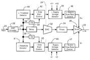
- FIG. 4 is a block diagram of circuitry for a high-efficiency line driver in accordance with the invention.
- the circuitry shown in FIG. 4 illustrates a part of a DMT encoder and line driver which may be used, for example, in an ADSL communications system to communicate digital input signals at an input 20 to a line 22 in a manner well known in the art.
- a vertical-line 24 in FIG. 4 indicates a general separation of the components into digital circuits to the left and analog circuits to the right of the line 24 .
- the circuits may be implemented using digital signal processors (DSPs) or application specific integrated circuits (ASICs), which are well known in the art.
- DSPs digital signal processors
- ASICs application specific integrated circuits
- Digital signal input 20 is supplied to a DMT encoder 26 .
- the DMT encoder 26 outputs a signal on path 28 which is an encoded and gain scaled digital signal that includes a sign bit and a plurality of magnitude of bits.
- Digital signals applied to the path 28 are delayed by digital delay stage 30 to permit power supply switching, if required, before the encoded signal is delivered to a line driver 36 that applies the encoded signal to the line 22 .
- the encoded signal is converted to an analog signal by the digital-to-analog converter (DAC) 32 .
- the analog signal output by the DAC 32 is filtered by analog filters 34 and amplified and buffered by the driver whose output is coupled to the line 22 .
- the DMT encoder 26 , DAC 32 , analog filters 34 and the driver 36 may be standard components known in the art.
- the delay stage 30 may also be a standard component.
- the delay stage 30 may optionally be incorporated as buffering functions in the DMT encoder 26 or the DAC 32 .
- the line driver 26 is preferably a low distortion amplifier having a push-pull class AB output stage that is provided with a positive supply voltage +V and a negative supply voltage ⁇ V.
- the circuitry shown in FIG. 4 also includes a positive and a negative signal threshold detectors 40 , 41 ; slew start controllers 42 , 43 ; positive and negative supply voltage selectors 44 , 45 ; and, supply voltage slew rate control circuits 46 , 47 for controlling positive and negative supply voltages V+ and V ⁇ , as required to support the signal encoded by the DMT encoder 26 .
- the supply voltage selector 44 is controlled by an output of the threshold detector 40 and the slew start controller 42 to select the higher of the two power supplies for supplying voltage to the driver 36 .
- the supply voltage selector 44 selects either a higher voltage V 2 or a lower voltage V 1 for supplying a positive supply voltage V+ to the line driver 36 .
- the selected voltage is supplied through the slew rate control circuit 46 , which limits a rate of change of the positive supply voltage V+ between the voltages V 1 and V 2 , and vice versa, so that significant distortion is not introduced by the line driver 36 into signals coupled to the line 22 .
- the threshold detector 40 is responsive to the digital signal on path 18 to detect when an amplitude of the signal exceeds a predefined threshold that indicates that the signal cannot be supported by the output of the lower voltage V 1 .
- the slew start controller 42 receives output from the threshold detector 40 and the DMT encoder 28 via a half-wave rectifier 38 which selects the positive voltage of the signal.
- the slew start controller measures a peak amplitude of the signal and computes a variable delay between the crossing of the threshold detected by the threshold detector 40 and switching on the power supply, as will be described below with reference to FIG. 5 .
- the delay stage 20 in the circuitry shown in FIG. 4 provides a signal delay that is determined, in conjunction with other delays in the circuitry such as signal delays that may occur in the analog filters 34 , to ensure that a positive signal amplitude peak 14 (FIG. 2) is accommodated within the increased voltage region of the positive supply voltage V+ waveform. Consequently, the positive supply voltage V+ is incremented to the higher voltage V 2 when it is necessary to accommodate large positive signal amplitude peaks, and is switched back to the lower voltage V 1 when it is sufficient to support smaller positive signal amplitudes. Gradual transitions between the two voltages to maintain low distortion is governed by the slew rate control 46 , as described above.
- the negative signal threshold detector 41 , slew start controller 43 , supply voltage selector 45 and slew rate control 47 control a selection of the negative voltages minus V 1 and minus V 2 .
- the negative slew rate control circuit 47 operates in a corresponding but independent manner to control the rates of change from voltage ⁇ V 1 to ⁇ V 2 , and vice versa, in order to ensure that distortion is not introduced into the signal output by line driver 36 on line 22 .
- the half-wave rectifier 39 rectifies only the negative components of the DMT signal to the slew start control 43 , as described above with reference to the positive circuit.
- FIG. 5 is a block diagram illustrating the components of the slew start controller 42 , 43 shown in FIG. 4 .
- the digital circuitry shown in FIG. 4 is used to calculate the value Setup 31 Adj (see FIG. 3 ).
- the slew start controller 42 includes a peak measurement circuit, generally indicated by the reference 50 , and a delay calculation circuit, generally indicated by reference 52 .
- the value Setup ⁇ Adj is output by the delay calculation circuit 52 to a variable delay circuit 54 that preferably includes a coarse variable delay circuit 56 and a fine variable delay circuit 58 , as will be explained below in more detail.
- the slew start controller 42 further includes a counter 60 used to determine a duration of the ON time of the V 2 power supply, as will also be explained below.
- a falling edge detector 62 receives output from the threshold detector 40 (FIG. 4) and outputs a signal to the peak measurement circuit 50 .
- the peak measurement circuit 50 includes a comparator 66 , a multiplexer 68 and a register 70 .
- a value stored in the register 70 is the instantaneous value of the rectified DMT encoder signal supplied via path 78 to the register 70 when the signal is rising.
- the value in register 70 is held at the last peak amplitude when the instantaneous value of the signal is falling until the signal crosses the V 1 threshold (FIG. 3 ). At this point the register is reset to 0 with the falling edge of the signal as determined by the falling edge detector 62 .
- the value in register 70 is controlled by the comparator 66 and the multiplexer 68 .
- the value (X) of the rectified encoder signal output by the half-wave rectifier 38 (FIG. 4) is supplied to the comparator 66 , which likewise receives a value of the register 70 via path 72 .
- the comparator compares the value of X (instantaneous amplitude of the encoder signal) with Y (value stored in register 70 ). If X is greater than or equal to Y, path 74 is asserted and the multiplexer 68 outputs the rectified amplitude X on path 76 which is supplied via path 78 to the register 70 .
- the instantaneous amplitude of the encoded signal is stored in register 15 .
- the encoded signal passes peak amplitude, X is less than Y and the value output by the multiplexer 68 is the value of the register.
- the peak amplitude is output until the falling edge detector circuit 62 determines that the signal has fallen below threshold V 1 (FIG. 3 ).
- register 70 is reset to zero and the register thereafter begins accumulating the instantaneous amplitude of the signal.
- the value output over path 76 is likewise supplied to the delay calculation circuit 52 , which includes a subtraction circuit 79 for computing a value of 1 ⁇ V pk . It may also include an optional truncation circuit 80 that reduces the number of bits output by the subtraction circuit 79 , in order to control the length of a digital word output by a multiplier circuit 82 ,
- the multiplier circuit 82 accepts the bits and multiplies them times a value stored in a register 84 representative of the quantity 1/SLOPE.
- the register 84 is preferably programmable and set by an external processor in accordance with the SLOPE(s) of the power supply waveform(s).
- the resultant product is supplied via path 86 to the coarse variable delay circuit 56 and the fine variable delay circuit 58 .
- the product is preferably divided into P most significant bits and Q least significant bits.
- the coarse variable delay circuit 56 receives only the P most significant bits while the fine variable delay circuit 58 receives only the Q least significant bits.
- the value, Setup ⁇ Adj is split between P-MSB bits and Q-LSB bits that are applied to the respective coarse and fine variable delay circuits 56 , 58 . These circuits delay the start time of the supply voltage selector signal as a function of the instantaneous peak amplitude of the signal.
- the P-bits are applied to the coarse variable delay circuit 56 , which is clocked at a rate of CK 1 .
- CK 1 is the same as the clock rate of the DMT encoder 26 (FIG. 4 ).
- the Q-bits are applied to the fine variable delay circuit 58 , which is clocked at a rate CK 2 , that is 2 Q times faster than CK 1 . Clocking the output delay line at the CK 2 rate provides finer resolution in setting the slew start time. The splitting of the delay line in this fashion is preferable because it reduces the hardware as compared to a single delay line clocked at the higher rate CK 2 .
- the output of the slew start controller 42 is applied to the supply voltage selector 44 (FIG. 4 ).
- the delay circuits 56 , 58 could be replaced with digital counters (not shown). In that case, the counters preferably count down from the respective P and Q bits to zero, in order to determine an appropriate slew start delay.
- the respective counters are preferably clocked at the same rates as the delay circuits described above.
- variable delay line outputs a relatively small value.
- V 1 threshold value
- a variable delay line value will be near maximum.
- the rising edge counter 60 provides a fixed delay in the output signal of the threshold detector 40 to permit the peak measurement circuit 50 and the delay calculation circuit 52 to determine the delay (P and Q bits) for the coarse variable delay circuit 56 and fine variable delay circuit 58 . After the fixed delay, the output of the rising edge counter is passed to the delay circuits 56 , 58 which delay the signal for the period determined by P and Q, respectively.
- the signal is passed to a set/reset (SR) flip-flop which causes the supply voltage selector 44 to switch to the higher voltage supply.
- the rising counter 60 counts to a predetermined static value that is programmable.
- the falling edge counter 63 receives input from the falling edge detector 62 to provide a fixed delay when the falling edge detector 62 detects that the signal has fallen below the threshold voltage V 1 .
- the falling edge counter 52 outputs a signal to the SR flip-flop 59 , which causes the supply voltage selector 44 to reset (switch back to the primary power supply).
- the falling edge counter 63 is likewise programmable and is programmed to provide a delay suited to the high voltage power supply V 2 .
- FIG. 6 is a schematic diagram of a waveform of an encoder signal in which two consecutive peaks (V pk1 and V pk2 ) occur in the signal before the signal falls below a threshold (V 1 ) of a lower power supply.
- the peak that controls the slew start delay period depends on a distance ( ⁇ ) between the first and second peak. If ⁇ is long, the first peak will govern the slew start delay period. If A is short, the second peak may govern the slew start delay period. In either case, however, adequate voltage will be supplied to the driver because the voltage supplied by the higher power supply will continue to rise until it reaches maximum voltage (V 2 ) or the higher power supply is turned off by the falling edge counter 63 (FIG. 5) after the signal falls below the threshold (V 1 ), as explained above.
- circuitry shown in FIG. 5 is duplicated for the negative side of the control circuitry (FIG. 4) in slew start controller 43 .
- variable delay output by slew start control 42 , 43 could be calculated N ⁇ 1 times, as required.
Abstract
Description
Claims (19)
Priority Applications (1)
| Application Number | Priority Date | Filing Date | Title |
|---|---|---|---|
| US09/526,176 US6333654B1 (en) | 2000-03-15 | 2000-03-15 | Variable power supply technique for use with a high efficiency line driver |
Applications Claiming Priority (1)
| Application Number | Priority Date | Filing Date | Title |
|---|---|---|---|
| US09/526,176 US6333654B1 (en) | 2000-03-15 | 2000-03-15 | Variable power supply technique for use with a high efficiency line driver |
Publications (1)
| Publication Number | Publication Date |
|---|---|
| US6333654B1 true US6333654B1 (en) | 2001-12-25 |
Family
ID=24096230
Family Applications (1)
| Application Number | Title | Priority Date | Filing Date |
|---|---|---|---|
| US09/526,176 Expired - Fee Related US6333654B1 (en) | 2000-03-15 | 2000-03-15 | Variable power supply technique for use with a high efficiency line driver |
Country Status (1)
| Country | Link |
|---|---|
| US (1) | US6333654B1 (en) |
Cited By (22)
| Publication number | Priority date | Publication date | Assignee | Title |
|---|---|---|---|---|
| US20020103745A1 (en) * | 2000-12-29 | 2002-08-01 | Abb Ab | System, method and computer program product for enhancing commercial value of electrical power produced from a renewable energy power production facility |
| US20020120878A1 (en) * | 2001-02-28 | 2002-08-29 | Lapidus Peter D. | Integrated circuit having programmable voltage level line drivers and method of operation |
| US20020161953A1 (en) * | 2001-04-30 | 2002-10-31 | Kotlowski Kenneth James | Bus arbitrator supporting multiple isochronous streams in a split transactional unidirectional bus architecture and method of operation |
| US6515523B1 (en) * | 2001-05-23 | 2003-02-04 | National Semiconductor Corporation | Method and apparatus for generating a power-on reset with an adjustable falling edge for power management |
| US6617895B2 (en) * | 2001-03-30 | 2003-09-09 | Intel Corporation | Method and device for symmetrical slew rate calibration |
| US6785758B1 (en) | 2001-06-01 | 2004-08-31 | Advanced Micro Devices, Inc. | System and method for machine specific register addressing in a split transactional unidirectional bus architecture |
| US20040213356A1 (en) * | 2003-04-24 | 2004-10-28 | Burke Joseph Patrick | Combined digital-to-analog converter and signal filter |
| US20040225781A1 (en) * | 2001-04-30 | 2004-11-11 | Kotlowski Kenneth James | Split transactional unidirectional bus architecture and method of operation |
| US6836168B1 (en) * | 2002-10-02 | 2004-12-28 | Xilinx, Inc. | Line driver with programmable slew rates |
| US6978014B1 (en) * | 2001-11-19 | 2005-12-20 | Alcatel | Apparatus for providing power to line drivers in a communication system |
| US20050285646A1 (en) * | 2004-06-29 | 2005-12-29 | Rashid Mamun U | Closed-loop control of driver slew rate |
| US7031378B1 (en) * | 2000-06-23 | 2006-04-18 | Globespan, Inc. | Unified DSL transceiver |
| US7209518B1 (en) * | 2000-08-03 | 2007-04-24 | Mks Instruments, Inc. | Higher PWM resolution for switchmode power supply control |
| US20070126410A1 (en) * | 2005-12-05 | 2007-06-07 | Texas Instruments Incorporated | System and method for implementing high-resolution delay |
| US20090201046A1 (en) * | 2005-03-22 | 2009-08-13 | Dong Pan | Output buffer and method having a supply voltage insensitive slew rate |
| US20100253420A1 (en) * | 2009-04-07 | 2010-10-07 | Futurewei Technologies, Inc. | Power Efficiency of a Line Driver |
| DE102009054168A1 (en) * | 2009-11-23 | 2011-05-26 | Marquardt Gmbh | Interface for use in electronic closing system utilized as door closing system for access authorization to transmit data of passenger car, has filter for dimensioning raising edges, where slopes of raising and falling edges are different |
| US8564920B1 (en) | 2010-07-22 | 2013-10-22 | Adtran, Inc. | Smart breaker and related system and method for protecting electrical devices from fault conditions |
| US8564922B1 (en) | 2010-07-22 | 2013-10-22 | Adtran, Inc. | System and method for protecting telecommunications device from power faults |
| US8693679B1 (en) | 2010-07-22 | 2014-04-08 | Adtran, Inc. | Communications system and associated method for reducing power consumption of a telecommunications device |
| US9614506B1 (en) * | 2015-12-03 | 2017-04-04 | Texas Instruments Incorporated | Digital pre-compensation for voltage slewing in a power converter |
| CN111314251A (en) * | 2014-03-25 | 2020-06-19 | 索尼公司 | Transmitter, communication system, and electronic apparatus |
Citations (3)
| Publication number | Priority date | Publication date | Assignee | Title |
|---|---|---|---|---|
| US5557233A (en) * | 1994-09-30 | 1996-09-17 | Vlsi Technology, Inc. | Filter for computer bus signals |
| US5717349A (en) * | 1994-10-24 | 1998-02-10 | Omega Telemus Inc. | Wideband digital peak detector |
| US6028468A (en) | 1994-04-15 | 2000-02-22 | Stmicroelectronics S.R. L. | Voltage-level shifter |
-
2000
- 2000-03-15 US US09/526,176 patent/US6333654B1/en not_active Expired - Fee Related
Patent Citations (3)
| Publication number | Priority date | Publication date | Assignee | Title |
|---|---|---|---|---|
| US6028468A (en) | 1994-04-15 | 2000-02-22 | Stmicroelectronics S.R. L. | Voltage-level shifter |
| US5557233A (en) * | 1994-09-30 | 1996-09-17 | Vlsi Technology, Inc. | Filter for computer bus signals |
| US5717349A (en) * | 1994-10-24 | 1998-02-10 | Omega Telemus Inc. | Wideband digital peak detector |
Cited By (40)
| Publication number | Priority date | Publication date | Assignee | Title |
|---|---|---|---|---|
| US7031378B1 (en) * | 2000-06-23 | 2006-04-18 | Globespan, Inc. | Unified DSL transceiver |
| US7209518B1 (en) * | 2000-08-03 | 2007-04-24 | Mks Instruments, Inc. | Higher PWM resolution for switchmode power supply control |
| US10135253B2 (en) * | 2000-12-29 | 2018-11-20 | Abb Schweiz Ag | System, method and computer program product for enhancing commercial value of electrical power produced from a renewable energy power production facility |
| US20020103745A1 (en) * | 2000-12-29 | 2002-08-01 | Abb Ab | System, method and computer program product for enhancing commercial value of electrical power produced from a renewable energy power production facility |
| US20020120878A1 (en) * | 2001-02-28 | 2002-08-29 | Lapidus Peter D. | Integrated circuit having programmable voltage level line drivers and method of operation |
| US7058823B2 (en) * | 2001-02-28 | 2006-06-06 | Advanced Micro Devices, Inc. | Integrated circuit having programmable voltage level line drivers and method of operation |
| US6864731B2 (en) | 2001-03-30 | 2005-03-08 | Intel Corporation | Method and device for symmetrical slew rate calibration |
| US6617895B2 (en) * | 2001-03-30 | 2003-09-09 | Intel Corporation | Method and device for symmetrical slew rate calibration |
| US20030201811A1 (en) * | 2001-03-30 | 2003-10-30 | Zumkehr John F. | Method and device for symmetrical slew rate calibration |
| US7046062B2 (en) | 2001-03-30 | 2006-05-16 | Intel Corporation | Method and device for symmetrical slew rate calibration |
| US20050189975A1 (en) * | 2001-03-30 | 2005-09-01 | Zumkehr John F. | Method and device for symmetrical slew rate calibration |
| US6813673B2 (en) | 2001-04-30 | 2004-11-02 | Advanced Micro Devices, Inc. | Bus arbitrator supporting multiple isochronous streams in a split transactional unidirectional bus architecture and method of operation |
| US6912611B2 (en) | 2001-04-30 | 2005-06-28 | Advanced Micro Devices, Inc. | Split transactional unidirectional bus architecture and method of operation |
| US20040225781A1 (en) * | 2001-04-30 | 2004-11-11 | Kotlowski Kenneth James | Split transactional unidirectional bus architecture and method of operation |
| US20020161953A1 (en) * | 2001-04-30 | 2002-10-31 | Kotlowski Kenneth James | Bus arbitrator supporting multiple isochronous streams in a split transactional unidirectional bus architecture and method of operation |
| US6515523B1 (en) * | 2001-05-23 | 2003-02-04 | National Semiconductor Corporation | Method and apparatus for generating a power-on reset with an adjustable falling edge for power management |
| US7185128B1 (en) | 2001-06-01 | 2007-02-27 | Advanced Micro Devices, Inc. | System and method for machine specific register addressing in external devices |
| US6785758B1 (en) | 2001-06-01 | 2004-08-31 | Advanced Micro Devices, Inc. | System and method for machine specific register addressing in a split transactional unidirectional bus architecture |
| US6978014B1 (en) * | 2001-11-19 | 2005-12-20 | Alcatel | Apparatus for providing power to line drivers in a communication system |
| US6836168B1 (en) * | 2002-10-02 | 2004-12-28 | Xilinx, Inc. | Line driver with programmable slew rates |
| CN1810002B (en) * | 2003-04-24 | 2010-11-10 | 高通股份有限公司 | Combined digital-to-analog converter and signal filter |
| WO2004098062A3 (en) * | 2003-04-24 | 2005-08-11 | Qualcomm Inc | Combined digital-to-analog converter and signal filter |
| US20040213356A1 (en) * | 2003-04-24 | 2004-10-28 | Burke Joseph Patrick | Combined digital-to-analog converter and signal filter |
| US7109768B2 (en) * | 2004-06-29 | 2006-09-19 | Intel Corporation | Closed-loop control of driver slew rate |
| US20050285646A1 (en) * | 2004-06-29 | 2005-12-29 | Rashid Mamun U | Closed-loop control of driver slew rate |
| US20090201046A1 (en) * | 2005-03-22 | 2009-08-13 | Dong Pan | Output buffer and method having a supply voltage insensitive slew rate |
| US7795903B2 (en) * | 2005-03-22 | 2010-09-14 | Micron Technology, Inc. | Output buffer and method having a supply voltage insensitive slew rate |
| US20070126410A1 (en) * | 2005-12-05 | 2007-06-07 | Texas Instruments Incorporated | System and method for implementing high-resolution delay |
| US7737671B2 (en) | 2005-12-05 | 2010-06-15 | Texas Instruments Incorporated | System and method for implementing high-resolution delay |
| US20100253420A1 (en) * | 2009-04-07 | 2010-10-07 | Futurewei Technologies, Inc. | Power Efficiency of a Line Driver |
| US8693676B2 (en) * | 2009-04-07 | 2014-04-08 | Futurewei Technologies, Inc. | Power efficiency of a line driver |
| US9036813B2 (en) | 2009-04-07 | 2015-05-19 | Futurewei Technologies, Inc. | Power efficiency of a line driver |
| DE102009054168A1 (en) * | 2009-11-23 | 2011-05-26 | Marquardt Gmbh | Interface for use in electronic closing system utilized as door closing system for access authorization to transmit data of passenger car, has filter for dimensioning raising edges, where slopes of raising and falling edges are different |
| US8564920B1 (en) | 2010-07-22 | 2013-10-22 | Adtran, Inc. | Smart breaker and related system and method for protecting electrical devices from fault conditions |
| US8564922B1 (en) | 2010-07-22 | 2013-10-22 | Adtran, Inc. | System and method for protecting telecommunications device from power faults |
| US8693679B1 (en) | 2010-07-22 | 2014-04-08 | Adtran, Inc. | Communications system and associated method for reducing power consumption of a telecommunications device |
| CN111314251A (en) * | 2014-03-25 | 2020-06-19 | 索尼公司 | Transmitter, communication system, and electronic apparatus |
| CN111314251B (en) * | 2014-03-25 | 2022-11-18 | 索尼公司 | Transmitter, communication system, and electronic apparatus |
| US11606795B2 (en) | 2014-03-25 | 2023-03-14 | Sony Group Corporation | Transmitter and communication system |
| US9614506B1 (en) * | 2015-12-03 | 2017-04-04 | Texas Instruments Incorporated | Digital pre-compensation for voltage slewing in a power converter |
Similar Documents
| Publication | Publication Date | Title |
|---|---|---|
| US6333654B1 (en) | Variable power supply technique for use with a high efficiency line driver | |
| US7573249B2 (en) | Power array system and method | |
| US7265522B2 (en) | Dynamic multiphase operation | |
| US7916506B2 (en) | Control device for use in a resonant direct current/direct current converter | |
| US7595692B2 (en) | Automatic gain control circuit | |
| US20190207575A1 (en) | Power supply for class g amplifier | |
| EP1097414A1 (en) | Improved power factor correction method and apparatus | |
| EP0442287A2 (en) | A direct current power supply device | |
| US11552546B2 (en) | Multi-phase power supply dynamic response control circuit and control method | |
| CN112202317A (en) | Grid driving device and power conversion device | |
| US8836311B2 (en) | Power converter with switching circuits | |
| US20060104343A1 (en) | PWM generator providing improved duty cycle resolution | |
| US5412341A (en) | Power control apparatus and method for a radio frequency amplifier | |
| US20240106394A1 (en) | Power supply circuit, power supply method, audio power amplifier and integrated circuit | |
| EP1364455B1 (en) | Generator control circuit | |
| US6798254B2 (en) | Dynamic control of switching reference voltage | |
| US4600983A (en) | Digital current regulator circuit for control of bidirectional current flow through a load | |
| JPH07226683A (en) | A/d converter | |
| CN115694128A (en) | Method and apparatus for adaptive output sampling for power converters | |
| JPH07170726A (en) | Method and device for controlling power voltage | |
| CN113452237A (en) | Power supply controller capable of reducing audio noise and method for reducing audio noise | |
| CA2361967A1 (en) | A system and method for reducing power dissipation for dsl circuits |
Legal Events
| Date | Code | Title | Description |
|---|---|---|---|
| AS | Assignment |
Owner name: NORTEL NETWORKS CORPORATION, CANADA Free format text: ASSIGNMENT OF ASSIGNORS INTEREST;ASSIGNORS:HARRIS, G. KATE;MITCHLER, DENNIS W.;REEL/FRAME:010629/0687 Effective date: 20000313 |
|
| AS | Assignment |
Owner name: NORTEL NETWORKS LIMITED, CANADA Free format text: CHANGE OF NAME;ASSIGNOR:NORTEL NETWORKS CORPORATION;REEL/FRAME:011195/0706 Effective date: 20000830 Owner name: NORTEL NETWORKS LIMITED,CANADA Free format text: CHANGE OF NAME;ASSIGNOR:NORTEL NETWORKS CORPORATION;REEL/FRAME:011195/0706 Effective date: 20000830 |
|
| FEPP | Fee payment procedure |
Free format text: PAYOR NUMBER ASSIGNED (ORIGINAL EVENT CODE: ASPN); ENTITY STATUS OF PATENT OWNER: LARGE ENTITY |
|
| REMI | Maintenance fee reminder mailed | ||
| LAPS | Lapse for failure to pay maintenance fees | ||
| STCH | Information on status: patent discontinuation |
Free format text: PATENT EXPIRED DUE TO NONPAYMENT OF MAINTENANCE FEES UNDER 37 CFR 1.362 |
|
| FP | Lapsed due to failure to pay maintenance fee |
Effective date: 20051225 |