US6339243B1 - High voltage device and method for fabricating the same - Google Patents
High voltage device and method for fabricating the same Download PDFInfo
- Publication number
- US6339243B1 US6339243B1 US09/517,303 US51730300A US6339243B1 US 6339243 B1 US6339243 B1 US 6339243B1 US 51730300 A US51730300 A US 51730300A US 6339243 B1 US6339243 B1 US 6339243B1
- Authority
- US
- United States
- Prior art keywords
- region
- conduction type
- semiconductor layer
- electrode
- impurity region
- Prior art date
- Legal status (The legal status is an assumption and is not a legal conclusion. Google has not performed a legal analysis and makes no representation as to the accuracy of the status listed.)
- Expired - Lifetime
Links
- 238000000034 method Methods 0.000 title claims description 26
- 239000004065 semiconductor Substances 0.000 claims abstract description 154
- 239000012535 impurity Substances 0.000 claims abstract description 91
- 239000000758 substrate Substances 0.000 claims abstract description 52
- 238000002955 isolation Methods 0.000 claims description 29
- 238000009792 diffusion process Methods 0.000 claims description 11
- 229910021420 polycrystalline silicon Inorganic materials 0.000 claims description 8
- 229920005591 polysilicon Polymers 0.000 claims description 8
- XUIMIQQOPSSXEZ-UHFFFAOYSA-N Silicon Chemical compound [Si] XUIMIQQOPSSXEZ-UHFFFAOYSA-N 0.000 description 22
- 229910052710 silicon Inorganic materials 0.000 description 22
- 239000010703 silicon Substances 0.000 description 22
- 230000005684 electric field Effects 0.000 description 21
- 230000015556 catabolic process Effects 0.000 description 6
- 230000008901 benefit Effects 0.000 description 5
- 229920002120 photoresistant polymer Polymers 0.000 description 4
- 239000012212 insulator Substances 0.000 description 2
- 150000002500 ions Chemical class 0.000 description 2
- 238000004519 manufacturing process Methods 0.000 description 2
- 239000000463 material Substances 0.000 description 2
- 238000012986 modification Methods 0.000 description 2
- 230000004048 modification Effects 0.000 description 2
- 230000015572 biosynthetic process Effects 0.000 description 1
- 230000003503 early effect Effects 0.000 description 1
- 238000005259 measurement Methods 0.000 description 1
- 238000012856 packing Methods 0.000 description 1
- 238000000059 patterning Methods 0.000 description 1
- 229920006395 saturated elastomer Polymers 0.000 description 1
Images


Classifications
-
- H—ELECTRICITY
- H01—ELECTRIC ELEMENTS
- H01L—SEMICONDUCTOR DEVICES NOT COVERED BY CLASS H10
- H01L29/00—Semiconductor devices adapted for rectifying, amplifying, oscillating or switching, or capacitors or resistors with at least one potential-jump barrier or surface barrier, e.g. PN junction depletion layer or carrier concentration layer; Details of semiconductor bodies or of electrodes thereof ; Multistep manufacturing processes therefor
- H01L29/66—Types of semiconductor device ; Multistep manufacturing processes therefor
- H01L29/68—Types of semiconductor device ; Multistep manufacturing processes therefor controllable by only the electric current supplied, or only the electric potential applied, to an electrode which does not carry the current to be rectified, amplified or switched
- H01L29/70—Bipolar devices
-
- H—ELECTRICITY
- H01—ELECTRIC ELEMENTS
- H01L—SEMICONDUCTOR DEVICES NOT COVERED BY CLASS H10
- H01L29/00—Semiconductor devices adapted for rectifying, amplifying, oscillating or switching, or capacitors or resistors with at least one potential-jump barrier or surface barrier, e.g. PN junction depletion layer or carrier concentration layer; Details of semiconductor bodies or of electrodes thereof ; Multistep manufacturing processes therefor
- H01L29/66—Types of semiconductor device ; Multistep manufacturing processes therefor
- H01L29/66007—Multistep manufacturing processes
- H01L29/66075—Multistep manufacturing processes of devices having semiconductor bodies comprising group 14 or group 13/15 materials
- H01L29/66227—Multistep manufacturing processes of devices having semiconductor bodies comprising group 14 or group 13/15 materials the devices being controllable only by the electric current supplied or the electric potential applied, to an electrode which does not carry the current to be rectified, amplified or switched, e.g. three-terminal devices
- H01L29/66234—Bipolar junction transistors [BJT]
- H01L29/66325—Bipolar junction transistors [BJT] controlled by field-effect, e.g. insulated gate bipolar transistors [IGBT]
-
- H—ELECTRICITY
- H01—ELECTRIC ELEMENTS
- H01L—SEMICONDUCTOR DEVICES NOT COVERED BY CLASS H10
- H01L29/00—Semiconductor devices adapted for rectifying, amplifying, oscillating or switching, or capacitors or resistors with at least one potential-jump barrier or surface barrier, e.g. PN junction depletion layer or carrier concentration layer; Details of semiconductor bodies or of electrodes thereof ; Multistep manufacturing processes therefor
- H01L29/66—Types of semiconductor device ; Multistep manufacturing processes therefor
- H01L29/68—Types of semiconductor device ; Multistep manufacturing processes therefor controllable by only the electric current supplied, or only the electric potential applied, to an electrode which does not carry the current to be rectified, amplified or switched
- H01L29/70—Bipolar devices
- H01L29/72—Transistor-type devices, i.e. able to continuously respond to applied control signals
- H01L29/739—Transistor-type devices, i.e. able to continuously respond to applied control signals controlled by field-effect, e.g. bipolar static induction transistors [BSIT]
- H01L29/7393—Insulated gate bipolar mode transistors, i.e. IGBT; IGT; COMFET
- H01L29/7394—Insulated gate bipolar mode transistors, i.e. IGBT; IGT; COMFET on an insulating layer or substrate, e.g. thin film device or device isolated from the bulk substrate
Definitions
- the present invention relates to a semiconductor device, and more particularly, to a high voltage device and a method for fabricating the same, in which a diode is used for reducing the influence of an electric field to silicon for enabling a higher operative voltage without an increased thickness of silicon on an upper portion thereof.
- a power MOSFET has an excellent switching speed compared to other semiconductor devices. Also, because it has a comparatively low withstand voltage (below 300V), it has a low turn-on resistance. Accordingly, a high voltage lateral power MOSFET is frequently used as a power device for a high density device packing.
- high voltage power devices there are, among others, DMOSFET (Double-diffused MOSFET), IGBT (Insulated Gate Bipolar Transistor), EDMOSFET (Extended Drain MOSFET) and LDMOSFET (Lateral Double-diffused MOSFET).
- the LDMOSFET has a variety of applications in chips, such as an HSD (High Side Driver), LSD (Low Side Driver) and an H-bridge circuit and can be fabricated easily
- the LDMOSFET has disadvantages in that it has a high threshold voltage, and a breakdown can occur at the surface of a silicon substrate in a drift region near a channel because the doping concentration in the channel region of the LDMOSFET is not uniform.
- a high voltage transistor developed recently to avoid the problems of earlier devices is an EDMOSFET.
- the silicon should be thick. The thicker the silicon, the more difficult it is to provide dielectric isolation between devices.
- SOI Silicon On Insulator
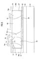
- FIG. 1 illustrates a section of the related art high voltage device.
- the related art high voltage device is provided with a first conduction type substrate 11 , a buried oxide film 12 formed on the substrate 11 , and a first conduction type semiconductor layer 13 formed on the buried oxide film 12 .
- a second conduction type drift region 14 is formed in the semiconductor layer 13
- a second conduction type well region 15 is formed in the second conduction type drift region 14 .
- a collector impurity region 16 is formed in the second conduction type well 15 region.
- a first conduction type drift region 17 is formed in the semiconductor layer 13 spaced from the second conduction type drift region 14 .
- a first conduction type well region 18 is formed in the first conduction type drift region 17
- an emitter impurity region 19 is formed in the first conduction type drift region 17
- a first insulating layer 20 is formed on the second conduction type drift region and extends to one side of the emitter impurity region 19 .
- a second insulating layer 21 is formed on the first conduction type drift region 14 between the collector impurity region 16 and the second conduction type drift region 17 .
- a gate electrode 22 is formed on the first insulating layer 20 and extends to overlap a portion of the second insulating layer 21 .
- a third insulating layer 23 is formed on the second insulating layer 21 and the gate electrode 22 .
- An emitter electrode 19 a insulated from the gate electrode 22 by the third insulating layer 23 , is electrically connected to the emitter impurity region 19 .
- a collector electrode 16 a is electrically connected to the collector impurity region 1 6 , and a field plate region 24 is formed to overlap with the gate electrode 22 with the third insulating layer 23 disposed therebetween.
- the field plate electrode 24 is formed to disperse an electric field formed in the second conduction type drift region 17 during operation to obtain a high breakdown voltage.
- an equipotential is applied both to the gate electrode 22 and the field plate electrode 24 , so that the depletion region in the second conduction type drift region 17 disperses an electric field concentrated on an edge portion of the gate electrode 22 . This is done to prevent a breakdown occurrence at the edge portion of the gate electrode.
- V is the breakdown voltage
- t s is the thickness of silicon
- t ox is the thickness of the buried oxide film
- E y is a critical electric field of the silicon in a vertical direction.
- FIG. 2 illustrates a voltage distribution of the related art high voltage device, wherefrom it can be understood that equipotential planes exist in the vertical direction as well as in a horizontal direction in an upper silicon layer. Furthermore, there are equipotential planes in a horizontal direction under the collector electrode, implying the presence of a vertical electric field therein.
- FIG. 3 illustrates the electric field under the collector electrode in the related art device. It can be understood that there is an electric field, not in the horizontal direction, but in the vertical direction, and that there are horizontal equipotential planes under the collector electrode.
- the vertical electric field shows a maximum in the vicinity of a junction between a P-conduction type upper silicon layer and an N-conduction type drift region. This means that the depletion layer is formed and an electric field is centered on the junction when a voltage is started to be applied to the collector electrode. Therefore, though the depletion layer becomes wider and the electric field becomes larger as the voltage to the collector electrode becomes higher, the position of the maximum electric field shows no change.
- FIG. 4 illustrates voltage vs. current of the collector when a voltage is applied to the gate electrode in the related art high voltage device. The measurements are obtained as a result of observation of the collector current as the collector voltage is increased after the application of a voltage to the gate electrode.
- the related art high voltage device has the following problems. As can be known from equation (1), the higher the breakdown voltage, the thicker the silicon layer in the wafer must be. The thicker silicon layer requires a deeper trench for the dielectric isolation technique, which is not possible to form in an actual process. In order not to form the thicker silicon layer in the fabrication of the high voltage device, either the thickness of the oxide film must be increased or a critical electric field on the silicon layer must be made larger. However, increasing the thickness of the buried oxide film causes deflection of the wafer due to material properties of the oxide film and the silicon layer. T his causes poor fabrication of the device.
- the present invention is directed to a high voltage device and a method for fabricating the same that substantially obviates one or more of the problems due to limitations and disadvantages of the related art.
- An object of the present invention is to provide a high voltage device and a method for fabricating the same, in which the influence of an electric field on a silicon layer is reduced for increasing an operative voltage of the high voltage device without increasing the thickness of the silicon layer.
- a high voltage device includes: a semiconductor substrate; a first semiconductor layer formed between an underlying first insulating layer and an overlying second insulating layer buried within the semiconductor substrate; first and second drift regions formed over the second insulating layer in the semiconductor substrate and spaced apart from each other; an emitter impurity region formed in the first drift region; a collector impurity region formed in the second drift region; a second semiconductor layer adjacent to and insulated from the collector impurity region, and connected to the first semiconductor layer; a third semiconductor layer adjacent to and insulated from the emitter impurity region, and connected to the first semiconductor layer; a gate electrode formed over and insulated from the first drift region adjacent to the emitter impurity region; an emitter electrode electrically connected to the emitter impurity region and the third semiconductor layer, the emitter electrode being insulated from the gate electrode; a collector electrode electrically connected to the collector impurity region and the second semiconductor layer; and,
- a high voltage device in another aspect of the present invention, includes: a semiconductor substrate; a first semiconductor layer formed between an underlying first insulating layer and an overlying second insulating layer buried within the semiconductor substrate; a third insulating layer surrounding a device isolation region above the second insulating layer in the semiconductor substrate; a first impurity region formed in the device isolation region; a second impurity region formed in the device isolation region and spaced apart from the first impurity region; a second semiconductor layer outside the device isolation region and connected to the first semiconductor layer; a third semiconductor layer outside the device isolation region and connected to the first semiconductor layer; a gate electrode over and insulated from the device isolation region and adjacent to the first impurity region; a fourth insulating layer over the gate electrode and the device isolation region; a first electrode electrically connected to the first impurity region and the third semiconductor layer; and, a second electrode electrically connected to the second impurity region and the second semiconductor layer.
- a method for fabricating a high voltage device includes: (1) forming a first insulating layer in a first conduction type substrate, a second conduction type first semiconductor layer on the first insulating layer, and a second insulating layer on the second conduction type first semiconductor layer; (2) dividing a portion of the substrate above the second insulating layer into first and second conduction type drift regions; (3) selectively removing the first and second conduction type drift regions and surrounding the remaining portions of the first and second conduction type drift regions with a third insulating layer to form a device isolation region; (4) forming a second conduction type second semiconductor layer and a first conduction type third semiconductor layer outside the device isolation region and each connected to the second conduction type first semiconductor layer; (5) forming an emitter impurity region in the first conduction type drift region and a collector impurity region in the second conduction type drift region in the device isolation region; (6) forming a gate electrode over the first conduction type drift region adjacent to the emitter impurity region;
- FIG. 1 illustrates a section of a related art high voltage device
- FIG. 2 illustrates a voltage distribution of a related art high voltage device
- FIG. 3 illustrates an electric field under a related art collector electrode
- FIG. 4 illustrates the voltage vs. current of a collector when a voltage is applied to a gate electrode in a related art high voltage device
- FIG. 5 illustrates a section of a high voltage device in accordance with a preferred embodiment of the present invention
- FIGS. 6A-6K illustrate sections showing the steps of a method for fabricating a high voltage device in accordance with a preferred embodiment of the present invention
- FIG. 7 illustrates a voltage distribution when a voltage is applied to a high voltage device of the present invention.
- FIG. 8 illustrates a current-voltage distribution of a high voltage device of the present invention.
- FIG. 5 illustrates a section of a high voltage device in accordance with a preferred embodiment of the present invention.
- the high voltage device in accordance with a preferred embodiment of the present invention includes a first conduction type semiconductor substrate 61 , a first insulating layer 62 formed on the semiconductor substrate 61 , and a second conduction type first semiconductor layer 63 formed on the first insulating layer 62 .
- a second insulating layer 64 is formed on the first semiconductor layer 63 .
- a second conduction type second semiconductor layer 68 a and a first conduction type third semiconductor layer 69 a are formed on respective opposite end portions of the first semiconductor layer 63 .
- a second conduction type drift region 65 and a first conduction type drift region 66 are spaced from each other between the second conduction type second semiconductor layer 68 a and the first conduction type third semiconductor layer 69 a.
- a buffer region 70 of a conduction type identical to the conduction type of the second semiconductor layer 68 a is formed in the second conduction type drift region 65 between the second conduction type second semiconductor layer 68 a and the third insulating layer 67 .
- a double diffusion region 71 is formed in the first conduction type first drift region 66 between the first conduction type third semiconductor layer 69 a and the third insulating layer 67 .
- a quasi LDD region 72 is formed in a surface of the first conduction type drift region 66 and an emitter impurity region 75 is formed in a surface of the double diffusion region 71 .
- a collector impurity region 76 is formed in a surface of the buffer region 70 .
- a gate electrode 74 is formed over the first conduction type drift region 66 with an insulating layer 73 there between. The gate electrode 74 is provided between the emitter impurity region 75 and the quasi LDD region 72 .
- An emitter electrode 75 a is formed insulated from the gate electrode 74 by a fourth insulating layer 77 and electrically connected to the emitter impurity region 75 .
- a collector electrode 76 a is formed insulated from the gate electrode 74 by the fourth insulating layer 77 and is electrically connected to the collector impurity region 76 .
- a field plate electrode 78 is formed on the fourth insulating layer 77 spaced from the collector electrode 76 a.
- the first conduction type is a P-conduction type
- the second conduction type is an N-conduction type.
- the third insulating layer 67 is a device isolation film for isolating devices.
- the first semiconductor layer and the second semiconductor layer are formed of polysilicon.
- the second conduction type first semiconductor layer 63 , the second conduction type second semiconductor layer 68 a , and the first conduction type third semiconductor layer 69 a form a diode.
- the cathode of the diode is connected to the emitter electrode 75 a
- an anode of the diode is connected to the collector electrode 76 a .
- the emitter electrode 75 a is connected to the emitter impurity region 75 .
- the collector electrode 76 a is connected to the collector impurity region 76 and the gate electrode 74 is connected to the foregoing electrodes form an IGBT. If the emitter impurity region is replaced with a source impurity region and the collector impurity region is replaced with a drain impurity region, the IGBT is replaced by an MOS transistor.
- FIGS. 6A-6K illustrate cross sections showing the steps of a method for fabricating a high voltage device in accordance with a preferred embodiment of the present invention.
- the method for fabricating a high voltage device in accordance with a preferred embodiment of the present invention starts with providing two semiconductor substrates, i.e., a first conduction type first semiconductor substrate 61 and the first conduction type second semiconductor substrate 61 a and forming a first insulating layer 62 on the first semiconductor substrate 61 .
- a second conduction type first semiconductor layer 63 is formed on the first insulating layer 62
- a second insulating layer 64 is formed on the second semiconductor substrate 61 a.
- the two semiconductor substrates 61 and 61 a are bonded together such that the second insulating layer 64 faces the first semiconductor layer 63 , to appear that the first insulating layer 62 , the first semiconductor layer 63 and the second insulating layer 64 are buried in a semiconductor substrate.
- the impurity concentration in the first semiconductor layer 63 to be doped is determined according to a required device voltage range.
- the thickness of the second insulating layer 64 should be sufficiently thin such that an electric field of the diode to be formed later will not affect the high voltage device.
- the first semiconductor layer 63 is formed of an N-conduction type polysilicon.
- the second semiconductor substrate on the second insulating layer is called an upper silicon layer 61 a for the sake of convenience, hereafter.
- a photoresist (not shown) is coated on the second semiconductor layer 61 a and subjected to patterning to expose a portion at which an N-type drift region is to be formed.
- the patterned photoresist is used as a mask for the process of injecting impurity ions to form a second conduction type drift region 65 in a portion of the second semiconductor substrate 61 a on the second insulating layer 64 .
- a photo process is conducted for forming a P-type drift region.
- photoresist is coated and patterned, to define a first conduction type drift region spaced from the second conduction type drift region 65 , and impurity ions are injected thereto, to form a first conduction type drift region 66 .
- the second conduction type drift region 65 and the first conduction type drift region 66 are spaced from each other by the second semiconductor substrate 61 a .
- the first conduction type is a P-conduction type
- the second conduction type is an N-conduction type.
- portions of the second insulating layer 64 on ends of the second conduction type drift region 65 and the first conduction type drift region 66 are etched to expose surfaces of the first semiconductor layer 63 .
- a third insulating layer 67 is formed on the exposed first semiconductor layer 63 and at sides of a second conduction type drift region 65 and the first conduction type drift region 66 .
- the third insulating layer 67 on the first silicon layer 63 is then removed to expose the first semiconductor layer 63 , again.
- a non-conductive second semiconductor layer 68 is formed over the exposed first semiconductor layer 63 , i.e., at a side of the second conduction type drift region 65 with the third insulating layer 67 therebetween, and a non-conductive third semiconductor layer 69 is formed at a side of the first conduction type drift region 66 with the third insulating layer 67 therebetween.
- a second conduction type impurity is doped in the second semiconductor layer 68 formed at a side of the second conduction type drift region 65 to change the semiconductor layer into a second conduction type second semiconductor layer 68 a .
- a first conduction type impurity is doped in the third semiconductor layer 69 at a side of the first conduction type drift region 66 to change the semiconductor layer into a first conduction type third semiconductor layer 69 a .
- Material of the first conduction type third semiconductor layer 69 a and the second conduction type second semiconductor layer 68 a include polysilicon.
- a high voltage diode is formed to comprise the first conduction type third semiconductor layer 69 a , the second conduction type first semiconductor layer 63 , and the second conduction type second semiconductor layer 68 a.
- the impurity doping is conducted even to dope the second conduction type drift region 65 to form a buffer region 70 in the second conduction type drift region 65 .
- a PN junction “A” comprising the first conduction type third semiconductor layer 69 a and the second conduction type first semiconductor layer 63 is formed under the first conduction type drift region 66 .
- the first conduction type impurity is injected into a portion of the first drift region 66 adjoining the third insulating layer 67 to form a double diffusion region 71 .
- a quasi LDD region 72 is formed in a surface of a portion of the first conduction type drift region 66 adjoining the second semiconductor substrate 61 a to form an IGBT channel.
- the quasi LDD region 72 is formed to prevent occurrence of a breakdown voltage at a junction surface of the diode with the first conduction type drift region 66 when a low voltage is applied to the collector electrode.
- a gate electrode 74 is formed over a top surface of the first conduction type drift region 66 between the double diffusion region 71 and the quasi LDD region 72 with a gate insulating film 73 provided therebetween.
- an emitter impurity region 75 is formed in a surface of the double diffusion region 71 on one side of the gate electrode 74 .
- a collector impurity region 76 is formed in a surface of a portion of the buffer region 70 adjoining to the third insulating layer 67 .
- a fourth insulating layer 77 is formed on the gate electrode 74 , a portion of the emitter impurity region 75 and a portion of the collector region 76 .
- An emitter electrode 75 a is formed which is electrically connected to the emitter impurity region 75 and overlaps the fourth insulating layer 77 .
- a field plate electrode 78 is formed on a given region of the fourth insulating layer 77 to be spaced from the emitter electrode 75 a .
- FIG. 7 illustrates a voltage distribution when a voltage is applied to the high voltage device of the present invention.
- a voltage distribution of the second semiconductor substrate shows vertical equipotential lines, with a horizontal electric field formed therein. Since there is no depletion layer in the second semiconductor substrate 61 a under the collector electrode, the electric field is transmitted to a portion under the second semiconductor substrate 61 a , and all voltage is present in the first insulating layer 62 .
- FIG. 8 illustrates a current-voltage distribution of a high voltage device of the present invention.
- FIG. 8 shows a relationship between voltages and currents of the collector when the high voltage device of the present invention is operated. It can be seen that the current flows normally when the gate voltage is 5V or 9V. When the gate voltage is 15V, the current exhibits an early effect which is a characteristic of a bipolar junction transistor (BJT). This is because the high voltage device of the present invention is an IGBT (Insulator Gate Bipolar Transistor) added with the BJT characteristic.
- IGBT Insulator Gate Bipolar Transistor
- the high voltage device and the method for fabricating the same have the following advantages.
- the second semiconductor substrate becomes free from an influence of the electric field.
- a limiting factor of the device performance can be eliminated. That is, by eliminating a vertical electric field from under the collector electrode, the thickness dependency of the second semiconductor substrate on a high voltage is eliminated, and a dielectric isolation is allowed. This enables the free selection of the thickness of the second semiconductor substrate (the upper silicon) to be consistent to the desired device performance.
Abstract
Description

Claims (24)
Applications Claiming Priority (2)
| Application Number | Priority Date | Filing Date | Title |
|---|---|---|---|
| KR1019990007178A KR100290913B1 (en) | 1999-03-04 | 1999-03-04 | High voltage devicd and method for manufacturing the same |
| KR99-1778 | 1999-03-04 |
Publications (1)
| Publication Number | Publication Date |
|---|---|
| US6339243B1 true US6339243B1 (en) | 2002-01-15 |
Family
ID=19575597
Family Applications (1)
| Application Number | Title | Priority Date | Filing Date |
|---|---|---|---|
| US09/517,303 Expired - Lifetime US6339243B1 (en) | 1999-03-04 | 2000-03-02 | High voltage device and method for fabricating the same |
Country Status (3)
| Country | Link |
|---|---|
| US (1) | US6339243B1 (en) |
| JP (1) | JP3354127B2 (en) |
| KR (1) | KR100290913B1 (en) |
Cited By (7)
| Publication number | Priority date | Publication date | Assignee | Title |
|---|---|---|---|---|
| US6544828B1 (en) * | 2001-11-07 | 2003-04-08 | Taiwan Semiconductor Manufacturing Company | Adding a poly-strip on isolation's edge to improve endurance of high voltage NMOS on EEPROM |
| US20050200301A1 (en) * | 2000-12-21 | 2005-09-15 | Semiconductor Energy Laboratory Co., Ltd., A Japan Corporation | Light emitting device and method of manufacturing the same |
| US20050263771A1 (en) * | 2000-12-11 | 2005-12-01 | Semiconductor Energy Laboratory Co., Ltd., A Japan Corporation | Semiconductor device, and manufacturing method thereof |
| US20060273402A1 (en) * | 2005-06-02 | 2006-12-07 | Khemka Vishnu K | Semiconductor device and method of manufacture |
| US20120061753A1 (en) * | 2010-09-09 | 2012-03-15 | Kabushiki Kaisha Toshiba | Semiconductor device |
| CN107681003A (en) * | 2017-09-11 | 2018-02-09 | 西安电子科技大学 | A kind of elemental semiconductor transverse direction superjunction double-diffused transistor with polycyclic Electric Field Modulated substrate |
| CN113594241A (en) * | 2021-05-25 | 2021-11-02 | 广东美的白色家电技术创新中心有限公司 | IGBT device |
Families Citing this family (3)
| Publication number | Priority date | Publication date | Assignee | Title |
|---|---|---|---|---|
| JP4741569B2 (en) * | 2000-12-21 | 2011-08-03 | 株式会社半導体エネルギー研究所 | Light emitting device |
| JP4067819B2 (en) * | 2000-12-21 | 2008-03-26 | 株式会社半導体エネルギー研究所 | Light emitting device |
| KR100409093B1 (en) * | 2001-07-12 | 2003-12-11 | 주식회사 엘리아테크 | A high voltage device and method of wiring metal on it |
Citations (1)
| Publication number | Priority date | Publication date | Assignee | Title |
|---|---|---|---|---|
| US5793064A (en) * | 1996-09-24 | 1998-08-11 | Allen Bradley Company, Llc | Bidirectional lateral insulated gate bipolar transistor |
-
1999
- 1999-03-04 KR KR1019990007178A patent/KR100290913B1/en not_active IP Right Cessation
-
2000
- 2000-02-25 JP JP2000048775A patent/JP3354127B2/en not_active Expired - Lifetime
- 2000-03-02 US US09/517,303 patent/US6339243B1/en not_active Expired - Lifetime
Patent Citations (1)
| Publication number | Priority date | Publication date | Assignee | Title |
|---|---|---|---|---|
| US5793064A (en) * | 1996-09-24 | 1998-08-11 | Allen Bradley Company, Llc | Bidirectional lateral insulated gate bipolar transistor |
Cited By (22)
| Publication number | Priority date | Publication date | Assignee | Title |
|---|---|---|---|---|
| US9059216B2 (en) | 2000-12-11 | 2015-06-16 | Semiconductor Energy Laboratory Co., Ltd. | Semiconductor device, and manufacturing method thereof |
| US20050263771A1 (en) * | 2000-12-11 | 2005-12-01 | Semiconductor Energy Laboratory Co., Ltd., A Japan Corporation | Semiconductor device, and manufacturing method thereof |
| US8421135B2 (en) | 2000-12-11 | 2013-04-16 | Semiconductor Energy Laboratory Co., Ltd. | Semiconductor device, and manufacturing method thereof |
| US10665610B2 (en) | 2000-12-11 | 2020-05-26 | Semiconductor Energy Laboratory Co., Ltd. | Semiconductor device, and manufacturing method thereof |
| US9666601B2 (en) | 2000-12-11 | 2017-05-30 | Semiconductor Energy Laboratory Co., Ltd. | Semiconductor device, and manufacturing method thereof |
| US7459352B2 (en) | 2000-12-11 | 2008-12-02 | Semiconductor Energy Laboratory Co., Ltd. | Semiconductor device, and manufacturing method thereof |
| US20090146149A1 (en) * | 2000-12-11 | 2009-06-11 | Semiconductor Energy Laboratory Co., Ltd. | Semiconductor device, and manufacturing method thereof |
| US9231044B2 (en) | 2000-12-21 | 2016-01-05 | Semiconductor Energy Laboratory Co., Ltd. | Light emitting device and method of manufacturing the same |
| US20090321753A1 (en) * | 2000-12-21 | 2009-12-31 | Semiconductor Energy Laboratory Co., Ltd. | Light Emitting Device and Method of Manufacturing the Same |
| US8013346B2 (en) | 2000-12-21 | 2011-09-06 | Semiconductor Energy Laboratory Co., Ltd. | Light emitting device and method of manufacturing the same |
| US9793335B2 (en) | 2000-12-21 | 2017-10-17 | Semiconductor Energy Laboratory Co., Ltd. | Light emitting device and method of manufacturing the same |
| US20050200301A1 (en) * | 2000-12-21 | 2005-09-15 | Semiconductor Energy Laboratory Co., Ltd., A Japan Corporation | Light emitting device and method of manufacturing the same |
| US7629618B2 (en) | 2000-12-21 | 2009-12-08 | Semiconductor Energy Laboratory Co., Ltd. | Light emitting device and method of manufacturing the same |
| US8735909B2 (en) | 2000-12-21 | 2014-05-27 | Semiconductor Energy Laboratory Co., Ltd. | Light emitting device and method of manufacturing the same |
| US6544828B1 (en) * | 2001-11-07 | 2003-04-08 | Taiwan Semiconductor Manufacturing Company | Adding a poly-strip on isolation's edge to improve endurance of high voltage NMOS on EEPROM |
| US7244989B2 (en) * | 2005-06-02 | 2007-07-17 | Freescale Semiconductor, Inc. | Semiconductor device and method of manufacture |
| US20060273402A1 (en) * | 2005-06-02 | 2006-12-07 | Khemka Vishnu K | Semiconductor device and method of manufacture |
| US8629505B2 (en) * | 2010-09-09 | 2014-01-14 | Kabushiki Kaisha Toshiba | Semiconductor device |
| US8884364B2 (en) | 2010-09-09 | 2014-11-11 | Kabushiki Kaisha Toshiba | Semiconductor device with field-plate electrode |
| US20120061753A1 (en) * | 2010-09-09 | 2012-03-15 | Kabushiki Kaisha Toshiba | Semiconductor device |
| CN107681003A (en) * | 2017-09-11 | 2018-02-09 | 西安电子科技大学 | A kind of elemental semiconductor transverse direction superjunction double-diffused transistor with polycyclic Electric Field Modulated substrate |
| CN113594241A (en) * | 2021-05-25 | 2021-11-02 | 广东美的白色家电技术创新中心有限公司 | IGBT device |
Also Published As
| Publication number | Publication date |
|---|---|
| JP2000260990A (en) | 2000-09-22 |
| KR100290913B1 (en) | 2001-05-15 |
| JP3354127B2 (en) | 2002-12-09 |
| KR20000059529A (en) | 2000-10-05 |
Similar Documents
| Publication | Publication Date | Title |
|---|---|---|
| EP0682811B1 (en) | Lateral semiconductor-on-insulator (soi) semiconductor device having a buried diode | |
| US6849880B1 (en) | Power semiconductor device | |
| US8237195B2 (en) | Power MOSFET having a strained channel in a semiconductor heterostructure on metal substrate | |
| US20090057711A1 (en) | Semiconductor device with a u-shape drift region | |
| US7825480B2 (en) | Power semiconductor device and manufacturing method of the same | |
| TWI804649B (en) | Insulated gate semiconductor device and method for fabricating a region of the insulated gate semiconductor device | |
| US20020182810A1 (en) | High power semiconductor device and fabrication method thereof | |
| KR100317458B1 (en) | Semiconductor component with linear current-to-voltage characteristics | |
| US8097921B2 (en) | Semiconductor device with high-breakdown-voltage transistor | |
| US11664449B2 (en) | LDMOS architecture and method for forming | |
| SE513284C3 (en) | Semiconductor component with linear current-to-voltage characteristics | |
| US20220359750A1 (en) | Transistor structure and manufacturing method of the same | |
| US6339243B1 (en) | High voltage device and method for fabricating the same | |
| US6268626B1 (en) | DMOS field effect transistor with improved electrical characteristics and method for manufacturing the same | |
| US11217691B2 (en) | High-voltage semiconductor devices having buried layer overlapped with source and well regions | |
| US20140322871A1 (en) | Partial soi on power device for breakdown voltage improvement | |
| US6730961B2 (en) | Semiconductor device | |
| JP3217488B2 (en) | High voltage semiconductor device | |
| EP4184590A1 (en) | Semiconductor device | |
| US11735657B2 (en) | Method for fabricating transistor structure | |
| US20230146397A1 (en) | Semiconductor device | |
| US20220190171A1 (en) | Semiconductor device | |
| JP3279092B2 (en) | Semiconductor device | |
| KR100479426B1 (en) | High-Voltage Device Structure and It's Fabrication Process | |
| KR101023079B1 (en) | Semiconductor device and method for manufacturing the device |
Legal Events
| Date | Code | Title | Description |
|---|---|---|---|
| AS | Assignment |
Owner name: HYUNDAI ELECTRONICS INDUSTRIES CO., LTD., KOREA, R Free format text: ASSIGNMENT OF ASSIGNORS INTEREST;ASSIGNORS:KWON, OH KYONG;JIN, JUN HEE;REEL/FRAME:010656/0276 Effective date: 20000219 |
|
| FEPP | Fee payment procedure |
Free format text: PAYOR NUMBER ASSIGNED (ORIGINAL EVENT CODE: ASPN); ENTITY STATUS OF PATENT OWNER: LARGE ENTITY |
|
| STCF | Information on status: patent grant |
Free format text: PATENTED CASE |
|
| AS | Assignment |
Owner name: HYNIX SEMICONDUCTOR INC., KOREA, REPUBLIC OF Free format text: CHANGE OF NAME;ASSIGNOR:HYUNDAI ELECTRONICS INDUSTRIES CO., LTD.;REEL/FRAME:015242/0899 Effective date: 20010329 |
|
| AS | Assignment |
Owner name: MAGNACHIP SEMICONDUCTOR, LTD., KOREA, REPUBLIC OF Free format text: ASSIGNMENT OF ASSIGNORS INTEREST;ASSIGNOR:HYNIX SEMICONDUCTOR, INC.;REEL/FRAME:016216/0649 Effective date: 20041004 |
|
| AS | Assignment |
Owner name: U.S. BANK NATIONAL ASSOCIATION, AS COLLATERAL TRUS Free format text: SECURITY INTEREST;ASSIGNOR:MAGNACHIP SEMICONDUCTOR, LTD.;REEL/FRAME:016470/0530 Effective date: 20041223 |
|
| FPAY | Fee payment |
Year of fee payment: 4 |
|
| FPAY | Fee payment |
Year of fee payment: 8 |
|
| FEPP | Fee payment procedure |
Free format text: PAYER NUMBER DE-ASSIGNED (ORIGINAL EVENT CODE: RMPN); ENTITY STATUS OF PATENT OWNER: LARGE ENTITY Free format text: PAYOR NUMBER ASSIGNED (ORIGINAL EVENT CODE: ASPN); ENTITY STATUS OF PATENT OWNER: LARGE ENTITY |
|
| AS | Assignment |
Owner name: MAGNACHIP SEMICONDUCTOR LTD.,KOREA, DEMOCRATIC PEO Free format text: RELEASE BY SECURED PARTY;ASSIGNOR:U.S. BANK NATIONAL ASSOCIATION;REEL/FRAME:024563/0807 Effective date: 20100527 |
|
| FPAY | Fee payment |
Year of fee payment: 12 |
|
| AS | Assignment |
Owner name: MAGNACHIP SEMICONDUCTOR LTD., KOREA, REPUBLIC OF Free format text: CORRECTIVE ASSIGNMENT TO CORRECT THE RECEIVING PARTY ADDRESS PREVIOUSLY RECORDED AT REEL: 024563 FRAME: 0807. ASSIGNOR(S) HEREBY CONFIRMS THE RELEASE BY SECURED PARTY;ASSIGNOR:US BANK NATIONAL ASSOCIATION;REEL/FRAME:034469/0001 Effective date: 20100527 |