US6339258B1 - Low resistivity tantalum - Google Patents
Low resistivity tantalum Download PDFInfo
- Publication number
- US6339258B1 US6339258B1 US09/347,221 US34722199A US6339258B1 US 6339258 B1 US6339258 B1 US 6339258B1 US 34722199 A US34722199 A US 34722199A US 6339258 B1 US6339258 B1 US 6339258B1
- Authority
- US
- United States
- Prior art keywords
- tantalum
- alpha
- interconnection structure
- copper
- barrier layer
- Prior art date
- Legal status (The legal status is an assumption and is not a legal conclusion. Google has not performed a legal analysis and makes no representation as to the accuracy of the status listed.)
- Expired - Lifetime
Links
Images


Classifications
-
- H—ELECTRICITY
- H01—ELECTRIC ELEMENTS
- H01L—SEMICONDUCTOR DEVICES NOT COVERED BY CLASS H10
- H01L21/00—Processes or apparatus adapted for the manufacture or treatment of semiconductor or solid state devices or of parts thereof
- H01L21/02—Manufacture or treatment of semiconductor devices or of parts thereof
- H01L21/04—Manufacture or treatment of semiconductor devices or of parts thereof the devices having at least one potential-jump barrier or surface barrier, e.g. PN junction, depletion layer or carrier concentration layer
- H01L21/18—Manufacture or treatment of semiconductor devices or of parts thereof the devices having at least one potential-jump barrier or surface barrier, e.g. PN junction, depletion layer or carrier concentration layer the devices having semiconductor bodies comprising elements of Group IV of the Periodic System or AIIIBV compounds with or without impurities, e.g. doping materials
- H01L21/28—Manufacture of electrodes on semiconductor bodies using processes or apparatus not provided for in groups H01L21/20 - H01L21/268
-
- H—ELECTRICITY
- H01—ELECTRIC ELEMENTS
- H01L—SEMICONDUCTOR DEVICES NOT COVERED BY CLASS H10
- H01L23/00—Details of semiconductor or other solid state devices
- H01L23/52—Arrangements for conducting electric current within the device in operation from one component to another, i.e. interconnections, e.g. wires, lead frames
- H01L23/522—Arrangements for conducting electric current within the device in operation from one component to another, i.e. interconnections, e.g. wires, lead frames including external interconnections consisting of a multilayer structure of conductive and insulating layers inseparably formed on the semiconductor body
- H01L23/532—Arrangements for conducting electric current within the device in operation from one component to another, i.e. interconnections, e.g. wires, lead frames including external interconnections consisting of a multilayer structure of conductive and insulating layers inseparably formed on the semiconductor body characterised by the materials
- H01L23/53204—Conductive materials
- H01L23/53209—Conductive materials based on metals, e.g. alloys, metal silicides
- H01L23/53228—Conductive materials based on metals, e.g. alloys, metal silicides the principal metal being copper
- H01L23/53233—Copper alloys
-
- H—ELECTRICITY
- H01—ELECTRIC ELEMENTS
- H01L—SEMICONDUCTOR DEVICES NOT COVERED BY CLASS H10
- H01L23/00—Details of semiconductor or other solid state devices
- H01L23/52—Arrangements for conducting electric current within the device in operation from one component to another, i.e. interconnections, e.g. wires, lead frames
- H01L23/522—Arrangements for conducting electric current within the device in operation from one component to another, i.e. interconnections, e.g. wires, lead frames including external interconnections consisting of a multilayer structure of conductive and insulating layers inseparably formed on the semiconductor body
- H01L23/532—Arrangements for conducting electric current within the device in operation from one component to another, i.e. interconnections, e.g. wires, lead frames including external interconnections consisting of a multilayer structure of conductive and insulating layers inseparably formed on the semiconductor body characterised by the materials
- H01L23/53204—Conductive materials
- H01L23/53209—Conductive materials based on metals, e.g. alloys, metal silicides
- H01L23/53228—Conductive materials based on metals, e.g. alloys, metal silicides the principal metal being copper
- H01L23/53238—Additional layers associated with copper layers, e.g. adhesion, barrier, cladding layers
-
- H—ELECTRICITY
- H01—ELECTRIC ELEMENTS
- H01L—SEMICONDUCTOR DEVICES NOT COVERED BY CLASS H10
- H01L2924/00—Indexing scheme for arrangements or methods for connecting or disconnecting semiconductor or solid-state bodies as covered by H01L24/00
- H01L2924/0001—Technical content checked by a classifier
- H01L2924/0002—Not covered by any one of groups H01L24/00, H01L24/00 and H01L2224/00
Definitions
- the present invention relates to an alpha-phase tantalum exhibiting relatively low resistivity and a high degree of orientation and a method for fabricating the alpha-phase tantalum.
- the alpha-phase tantalum according to the present invention is especially useful as a barrier layer and particularly in copper chip interconnection structures.
- the alpha-phase tantalum acts as a redundant current layer in such structures and finds use in chip structures, packaging, flat panel displays and in magnetics.
- AlCu Aluminum and its related alloy, AlCu, are currently the predominantly used conductors for forming interconnection from electronic devices such as integrated circuits.
- the amount of Cu in AlCu is typically in the range of about 0.3 to about 4%.
- capping inhibits this diffusion.
- One widely suggested method of capping includes employing a conductive barrier layer along the sidewalls and bottom surface of a copper interconnect. Typical of such barrier layers is tantalum and titanium, and nitrides thereof. Capping of the upper surface of a copper interconnect usually employs silicon nitride.
- the tantalum employed is typically an alpha-phase tantalum layer, which besides acting as a barrier, also acts as a redundant current carrier layer to assist the main conductor copper in current distribution. Moreover, it becomes the main conductor in the event the copper fails due to electromigration.
- the resistivity of the presently available alpha-phase tantalum layer is typically about 25 micro ohm-cm. Although this resistivity is adequate, it leaves room for improvement. Accordingly, it would be desirable to reduce the resistivity of the redundant conducting layer to be as low as practical.
- the present invention relates to a tantalum layer having significantly reduced resistivity.
- the tantalum layer according to the present invention has a high degree of orientation. More particularly, the present invention relates to an alpha-phase tantalum having a resistivity of about 15 micro-ohm-cm or lower.
- the present invention also relates to a process for preparing the tantalum of the present invention.
- the process involves sputter deposition of tantalum employing a vacuum of at least about 1 ⁇ 10 E6 torr, power of about 0.5 to about 6 kilowatts, in the presence of an inert gas to provide an effective pressure of about 1 to about 10 millitorr.
- the present invention also relates to an interconnection structure for semiconductor integrated circuits which comprises a layer of copper or copper alloy and a barrier layer of alpha-phase tantalum having a resistivity of about 15 micro-ohm-cm or less.
- a further aspect of the present invention relates to an alpha-phase tantalum obtained by the above described process.
- FIG. 1 is a schematic diagram of a semiconductor structure in accordance with the present invention.
- FIG. 2 is an x-ray diffraction spectra for the alpha-tantalum of the present invention.
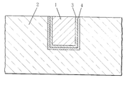
- copper wiring 1 is included on a semiconductor wafer (not shown) such as silicon, silicon-germanium alloys, silicon carbide, or gallium arsenide.
- the copper wiring 1 is electrically isolated by including an interlevel dielectric 2 such as silicon dioxide (SiO 2 ), phosphosilicate-glass (PSG), boron doped PSG (BDPSG) or tetraethylorthosilicate (TEOS).
- the dielectric can include low dielectric constant materials such as fluorinated SiO 2 , organic polymers and porous dielectrics.
- a barrier layer 3 of the alpha-phase tantalum of the present invention is employed along the bottom and side wall surfaces of the copper wiring 1 between the copper wiring 1 and insulator 2 .
- the copper wiring layer is typically about 1000 to about 20,000 ⁇ thick.
- the alpha-phase tantalum of the present invention has low resistivity of about 15 micron-ohm-cm or lower and is used both as the barrier layer and redundant current carrying layer.
- the alpha-phase tantalum layer, according to the present invention preferably is a relatively highly oriented film and has a ⁇ 110> diffraction peak at about 49° (2-theta) as demonstrated in FIG. 2 .
- the x-ray-diffraction spectra is measured by depositing a layer of the alpha-phase tantalum to a thickness of a few hundred angstroms, such as about 400 ⁇ , overtop a substrate of tantalum nitride using the process conditions to be discussed below.
- a 2-theta style x-ray-diffraction (XRD) scan is then performed and as shown in FIG. 2, the resulting spectra contains a very narrow diffraction peak.
- XRD x-ray-diffraction
- the alpha-phase tantalum layer of the present invention can be produced by employing sputter machines such as that available under the trade designation Endura 5500 from Applied Materials Corporation or sputter machines available from Novellus Corporation. Such are well known and need not be described herein in any detail.
- the sputter apparatus for purposes of the present invention use a DC magnetron source configuration and use as the source of tantalum, tantalum having a purity of about 99.9% or greater.
- an inert gas such as argon at a flow rate of about 50 to about 130 standard cubic centimeters per minute (sccm) is injected into the process cavity which contains the target along with the wafer upon which the tantalum is to be deposited.
- the process cavity prior to injection of the inert gas was previously evacuated to a vacuum level of at least 1.0 ⁇ 10 E6 torr using for example a cryogenic pump. Simultaneous to flowing the inert sputter gas, an additional gas flow of nitrogen is also begun at a flow rate of about 20 to about 60 standard cubic centimeters per minute. The process cavity is filled with both gases to achieve an effective pressure of about 1 to about 10 millitorr.
- the power typically employed to create a plasma for the purposes of the present invention is between about 0.5 and about 6 kilowatts, and preferably about 2 to about 3 kilowatts. Any combination of target voltage and current to achieve this power level can be employed.
- the material deposited is the highly oriented alpha-phase tantalum material of the present invention. The deposition rate is typically about 1000 to about 2000 ⁇ per minute and more typically about 1200 to about 1500 ⁇ per minute.
- the thickness of the alpha-phase tantalum barrier layer 3 is about 50 to about 300 ⁇ and more typically about 100 to about 200 ⁇ .
- a second barrier layer 4 is present between the alpha-tantalum barrier layer 3 and insulator 2 .
- This second barrier layer 4 is typically tantalum nitride, tantalum silicon, tantalum silicon nitride, titanium nitride, tungsten or tungsten nitride.
- the thickness of barrier layer 4 is typically about 25 to about 300 ⁇ and more typically about 50 to about 100 ⁇ .
Abstract
An alpha-phase tantalum having a resistivity of about 15 micro-ohm-cm or less is provided and is especially useful as a barrier layer for copper and copper alloy interconnections.
Description
The present invention relates to an alpha-phase tantalum exhibiting relatively low resistivity and a high degree of orientation and a method for fabricating the alpha-phase tantalum. In addition, the alpha-phase tantalum according to the present invention is especially useful as a barrier layer and particularly in copper chip interconnection structures. Furthermore, the alpha-phase tantalum acts as a redundant current layer in such structures and finds use in chip structures, packaging, flat panel displays and in magnetics.
Aluminum and its related alloy, AlCu, are currently the predominantly used conductors for forming interconnection from electronic devices such as integrated circuits. The amount of Cu in AlCu is typically in the range of about 0.3 to about 4%.
Replacement of AlCu by Cu and Cu alloys as a chip interconnection material results in advantages of improved chip performance. Performance is improved because the resistivity of Cu and in certain copper alloys is less than the resistivity of AlCu. Besides performance, high chip yield count and higher circuit wiring densities are also realized.
In addition, interest in using copper as interconnects in semiconductor devices has increased since it possesses a reduced susceptibility to electromigration failure as compared to the more traditional aluminum or aluminum alloy interconnects.
The advantages of copper metallization have been recognized by the entire semiconductor industry. Copper metallization has been the subject of extensive research documented by two entire issues of the Materials Research Society (MRS) Bulletin. One dedicated to academic research on the subject is MRS Bulletin, Vol. XVIII, No. 6 (June 1993) and the other dedicated to industrial research in MRS Bulletin, Vol. XIX, No. 8 (August 1994). A 1993 paper by Luther et al, “Planar Copper-Polyamide Back End of the Line Interconnection for ULSI Devices”, in Proc. IEEE VLSI Multilevel Interconnections Conference, Santa Clara, Calif., Jun. 8-9, 1993, p. 15, describes the fabrication of copper chip interconnections with four levels of metallization.
However, since copper has a tendency when used in interconnect metallurgy to diffuse into surrounding dielectric materials such as silicon dioxide, encapsulation of the copper is essential. The capping inhibits this diffusion. One widely suggested method of capping includes employing a conductive barrier layer along the sidewalls and bottom surface of a copper interconnect. Typical of such barrier layers is tantalum and titanium, and nitrides thereof. Capping of the upper surface of a copper interconnect usually employs silicon nitride.
The tantalum employed is typically an alpha-phase tantalum layer, which besides acting as a barrier, also acts as a redundant current carrier layer to assist the main conductor copper in current distribution. Moreover, it becomes the main conductor in the event the copper fails due to electromigration. However, the resistivity of the presently available alpha-phase tantalum layer is typically about 25 micro ohm-cm. Although this resistivity is adequate, it leaves room for improvement. Accordingly, it would be desirable to reduce the resistivity of the redundant conducting layer to be as low as practical.
The present invention relates to a tantalum layer having significantly reduced resistivity. In addition, the tantalum layer according to the present invention has a high degree of orientation. More particularly, the present invention relates to an alpha-phase tantalum having a resistivity of about 15 micro-ohm-cm or lower.
The present invention also relates to a process for preparing the tantalum of the present invention. In particular, the process involves sputter deposition of tantalum employing a vacuum of at least about 1×10 E6 torr, power of about 0.5 to about 6 kilowatts, in the presence of an inert gas to provide an effective pressure of about 1 to about 10 millitorr.
The present invention also relates to an interconnection structure for semiconductor integrated circuits which comprises a layer of copper or copper alloy and a barrier layer of alpha-phase tantalum having a resistivity of about 15 micro-ohm-cm or less.
A further aspect of the present invention relates to an alpha-phase tantalum obtained by the above described process.
Still other objects and advantages of the present invention will become readily apparent by those skilled in the art from the following detailed description, wherein it is shown and described only the preferred embodiments of the invention, simply by way of illustration of the best mode contemplated of carrying out the invention. As will be realized the invention is capable of other and different embodiments, and its several details are capable of modifications in various obvious respects, without departing from the invention. Accordingly, the description is to be regarded as illustrative in nature and not as restrictive.
FIG. 1 is a schematic diagram of a semiconductor structure in accordance with the present invention.
FIG. 2 is an x-ray diffraction spectra for the alpha-tantalum of the present invention.
In order to facilitate an understanding of the present invention, reference will be made to the figures.
As illustrated in FIG. 1, copper wiring 1 is included on a semiconductor wafer (not shown) such as silicon, silicon-germanium alloys, silicon carbide, or gallium arsenide. The copper wiring 1 is electrically isolated by including an interlevel dielectric 2 such as silicon dioxide (SiO2), phosphosilicate-glass (PSG), boron doped PSG (BDPSG) or tetraethylorthosilicate (TEOS). In addition, the dielectric can include low dielectric constant materials such as fluorinated SiO2, organic polymers and porous dielectrics.
According to the present invention, a barrier layer 3 of the alpha-phase tantalum of the present invention is employed along the bottom and side wall surfaces of the copper wiring 1 between the copper wiring 1 and insulator 2. The copper wiring layer is typically about 1000 to about 20,000 Å thick. The alpha-phase tantalum of the present invention has low resistivity of about 15 micron-ohm-cm or lower and is used both as the barrier layer and redundant current carrying layer. Furthermore, the alpha-phase tantalum layer, according to the present invention, preferably is a relatively highly oriented film and has a <110> diffraction peak at about 49° (2-theta) as demonstrated in FIG. 2. The x-ray-diffraction spectra is measured by depositing a layer of the alpha-phase tantalum to a thickness of a few hundred angstroms, such as about 400 Å, overtop a substrate of tantalum nitride using the process conditions to be discussed below. A 2-theta style x-ray-diffraction (XRD) scan is then performed and as shown in FIG. 2, the resulting spectra contains a very narrow diffraction peak. For an XRD set up using monochromatic iron radiation from a sealed tube source operating at 35 kilovolts and 35 milliamps, a <110> diffraction peak at about 49° (2-theta) is generated. This confirms the highly oriented nature of the alpha-phase tantalum film according to the present invention.
The alpha-phase tantalum layer of the present invention can be produced by employing sputter machines such as that available under the trade designation Endura 5500 from Applied Materials Corporation or sputter machines available from Novellus Corporation. Such are well known and need not be described herein in any detail. Typically, the sputter apparatus for purposes of the present invention use a DC magnetron source configuration and use as the source of tantalum, tantalum having a purity of about 99.9% or greater. In carrying out the process, an inert gas such as argon at a flow rate of about 50 to about 130 standard cubic centimeters per minute (sccm) is injected into the process cavity which contains the target along with the wafer upon which the tantalum is to be deposited. The process cavity prior to injection of the inert gas was previously evacuated to a vacuum level of at least 1.0×10 E6 torr using for example a cryogenic pump. Simultaneous to flowing the inert sputter gas, an additional gas flow of nitrogen is also begun at a flow rate of about 20 to about 60 standard cubic centimeters per minute. The process cavity is filled with both gases to achieve an effective pressure of about 1 to about 10 millitorr. The power typically employed to create a plasma for the purposes of the present invention is between about 0.5 and about 6 kilowatts, and preferably about 2 to about 3 kilowatts. Any combination of target voltage and current to achieve this power level can be employed. The material deposited is the highly oriented alpha-phase tantalum material of the present invention. The deposition rate is typically about 1000 to about 2000 Å per minute and more typically about 1200 to about 1500 Å per minute.
In a typical interconnection structure, the thickness of the alpha-phase tantalum barrier layer 3 is about 50 to about 300 Å and more typically about 100 to about 200 Å.
Additionally, and optionally, as illustrated in FIG. 1, a second barrier layer 4 is present between the alpha-tantalum barrier layer 3 and insulator 2. This second barrier layer 4 is typically tantalum nitride, tantalum silicon, tantalum silicon nitride, titanium nitride, tungsten or tungsten nitride. The thickness of barrier layer 4 is typically about 25 to about 300 Å and more typically about 50 to about 100 Å.
The following non-limiting examples are presented to further illustrate the present invention.
The foregoing description of the invention illustrates and describes the present invention. Additionally, the disclosure shows and describes only the preferred embodiments of the invention but, as mentioned above, it is to be understood that the invention is capable of use in various other combinations, modifications, and environments and is capable of changes or modifications within the scope of the inventive concept as expressed herein, commensurate with the above teachings and/or the skill or knowledge of the relevant art. The embodiments described hereinabove are further intended to explain best modes known of practicing the invention and to enable others skilled in the art to utilize the invention in such, or other, embodiments and with the various modifications required by the particular applications or uses of the invention. Accordingly, the description is not intended to limit the invention to the form disclosed herein. Also, it is intended that the appended claims be construed to include alternative embodiments.
Claims (17)
1. Alpha-phase tantalum having a resistivity of less than 15 micro-ohm-cm.
2. The alpha-phase tantalum of claim 1 having a <110> diffraction peak at about 49° (2-theta) as measured by x-ray diffraction using monochromatic iron radiation from a sealed tube source operating at 35 kilovolts and 35 milliamps.
3. The alpha-phase tantalum of claim 2 having the x-ray diffraction spectra as shown in FIG. 2.
4. An interconnection structure for semiconductor integrated circuits which comprises a layer of copper or copper alloy and a barrier layer of alpha-phase tantalum having a resistivity of less than 15 micro-ohm-cm.
5. The interconnection structure of claim 4 wherein the alpha-phase tantalum has a <110> diffraction peak at about 45° (2-theta) obtained by an x-ray diffraction scan using monochromatic iron radiation from a sealed tube source operating at 35 kilovolts and 35 milliamps.
6. The interconnection structure of claim 4 wherein the alpha-phase tantalum has an x-ray diffraction scan shown in FIG. 2.
7. The interconnection structure of claim 4 which further includes electrical isolation and wherein the barrier layer separates the copper from the isolation.
8. The interconnection structure of claim 4 wherein the thickness of the copper is about 200 to about 1500 Å.
9. The interconnection structure of claim 4 wherein the thickness of the alpha-phase tantalum layer is about 50 to about 300 Å.
10. The interconnection structure of claim 7 which further includes a second barrier layer between the insulation and the alpha-phase tantalum.
11. The interconnection structure of claim 10 wherein the second barrier layer is selected from the group consisting of tantalum nitride, tantalum silicon, tantalum silicon nitride, titanium nitride, tungsten and tungsten nitride.
12. The interconnection structure of claim 10 wherein the second barrier layer is tantalum nitride or titanium nitride.
13. The interconnection structure of claim 10 wherein the second barrier layer is tantalum nitride.
14. The interconnection structure of claim 10 wherein the thickness of the second barrier layer is about 25 to about 300 Å.
15. An interconnection structure for semiconductor integrated circuits which comprises a layer of copper or copper alloy and a barrier layer of alpha-phase tantalum having a resistivity of about 15 micro-ohm-cm or less, and
wherein the thickness of the copper is about 200 to about 1500 Å.
16. An interconnection structure for semiconductor integrated circuits which comprises a layer of copper or copper alloy and a barrier layer of alpha-phase tantalum having a resistivity of about 15 micro-ohm-cm or less, and
wherein the thickness of the alpha-phase tantalum layer is about 50 to about 300 Å.
17. The interconnection structure of claim 16 wherein the thickness of the copper is about 200 to about 1500 Å.
Priority Applications (7)
| Application Number | Priority Date | Filing Date | Title |
|---|---|---|---|
| US09/347,221 US6339258B1 (en) | 1999-07-02 | 1999-07-02 | Low resistivity tantalum |
| TW089105982A TW552692B (en) | 1999-07-02 | 2000-03-30 | Low resistivity tantalum |
| SG200003535A SG85196A1 (en) | 1999-07-02 | 2000-06-23 | Low resistivity tantalum |
| MYPI20002879 MY125124A (en) | 1999-07-02 | 2000-06-26 | Low resistivity tantalum |
| KR10-2000-0036028A KR100455988B1 (en) | 1999-07-02 | 2000-06-28 | Alpha-phase tantalum and Method for producing an alpha-phase tantalum and Interconnection structure for semiconductor integrated circuit |
| CNB001199102A CN1191589C (en) | 1999-07-02 | 2000-06-30 | Low resistivity tantalum |
| US09/988,775 US20020028579A1 (en) | 1999-07-02 | 2001-11-20 | Low resistivity tantalum |
Applications Claiming Priority (1)
| Application Number | Priority Date | Filing Date | Title |
|---|---|---|---|
| US09/347,221 US6339258B1 (en) | 1999-07-02 | 1999-07-02 | Low resistivity tantalum |
Related Child Applications (1)
| Application Number | Title | Priority Date | Filing Date |
|---|---|---|---|
| US09/988,775 Division US20020028579A1 (en) | 1999-07-02 | 2001-11-20 | Low resistivity tantalum |
Publications (1)
| Publication Number | Publication Date |
|---|---|
| US6339258B1 true US6339258B1 (en) | 2002-01-15 |
Family
ID=23362815
Family Applications (2)
| Application Number | Title | Priority Date | Filing Date |
|---|---|---|---|
| US09/347,221 Expired - Lifetime US6339258B1 (en) | 1999-07-02 | 1999-07-02 | Low resistivity tantalum |
| US09/988,775 Abandoned US20020028579A1 (en) | 1999-07-02 | 2001-11-20 | Low resistivity tantalum |
Family Applications After (1)
| Application Number | Title | Priority Date | Filing Date |
|---|---|---|---|
| US09/988,775 Abandoned US20020028579A1 (en) | 1999-07-02 | 2001-11-20 | Low resistivity tantalum |
Country Status (6)
| Country | Link |
|---|---|
| US (2) | US6339258B1 (en) |
| KR (1) | KR100455988B1 (en) |
| CN (1) | CN1191589C (en) |
| MY (1) | MY125124A (en) |
| SG (1) | SG85196A1 (en) |
| TW (1) | TW552692B (en) |
Cited By (16)
| Publication number | Priority date | Publication date | Assignee | Title |
|---|---|---|---|---|
| US6455418B1 (en) * | 1998-12-22 | 2002-09-24 | Agere Systems Guardian Corp. | Barrier for copper metallization |
| US6686662B2 (en) * | 2002-05-21 | 2004-02-03 | Agere Systems Inc. | Semiconductor device barrier layer |
| US20040082319A1 (en) * | 2002-10-25 | 2004-04-29 | Shaw Venson M. | Delivery of network services |
| US20040129999A1 (en) * | 2002-12-30 | 2004-07-08 | Jung Kyung Yun | Semiconductor device and method of manufacturing the same |
| US20040131878A1 (en) * | 2003-01-03 | 2004-07-08 | Seet Chim Seng | Method to form alpha phase Ta and its application to IC manufacturing |
| US20050001325A1 (en) * | 2003-07-03 | 2005-01-06 | International Business Machines Corporation | Selective capping of copper wiring |
| US20050031784A1 (en) * | 1999-08-16 | 2005-02-10 | Peijun Ding | Barrier layer for electroplating processes |
| US20050118796A1 (en) * | 2003-11-28 | 2005-06-02 | Chiras Stefanie R. | Process for forming an electrically conductive interconnect |
| US20060071338A1 (en) * | 2004-09-30 | 2006-04-06 | International Business Machines Corporation | Homogeneous Copper Interconnects for BEOL |
| US7157795B1 (en) * | 2004-09-07 | 2007-01-02 | Advanced Micro Devices, Inc. | Composite tantalum nitride/tantalum copper capping layer |
| US7256089B2 (en) * | 2001-09-24 | 2007-08-14 | Intel Corporation | Top electrode barrier for on-chip die de-coupling capacitor and method of making same |
| US8425757B2 (en) | 2005-07-20 | 2013-04-23 | Bayer Healthcare Llc | Gated amperometry |
| US20150001720A1 (en) * | 2013-06-27 | 2015-01-01 | Taiwan Semiconductor Manufacturing Co., Ltd. | Interconnect Structure and Method for Forming Interconnect Structure |
| WO2015138621A1 (en) | 2014-03-12 | 2015-09-17 | Invensas Corporation | Via structure for signal equalization |
| US9543199B2 (en) * | 2004-04-30 | 2017-01-10 | Infineon Technologies Ag | Long-term heat treated integrated circuit arrangements and methods for producing the same |
| US9933385B2 (en) | 2007-12-10 | 2018-04-03 | Ascensia Diabetes Care Holdings Ag | Method of using an electrochemical test sensor |
Families Citing this family (4)
| Publication number | Priority date | Publication date | Assignee | Title |
|---|---|---|---|---|
| JP2002343859A (en) * | 2001-05-15 | 2002-11-29 | Mitsubishi Electric Corp | Connection structure between wires and its manufacturing method |
| US6645853B1 (en) * | 2001-12-05 | 2003-11-11 | Advanced Micro Devices, Inc. | Interconnects with improved barrier layer adhesion |
| JP3954998B2 (en) * | 2003-08-11 | 2007-08-08 | ローム株式会社 | Semiconductor device and manufacturing method thereof |
| US7585764B2 (en) * | 2005-08-09 | 2009-09-08 | International Business Machines Corporation | VIA bottom contact and method of manufacturing same |
Citations (17)
| Publication number | Priority date | Publication date | Assignee | Title |
|---|---|---|---|---|
| JPS55132056A (en) | 1979-04-03 | 1980-10-14 | Toshiba Corp | Semiconductor device |
| JPS63156341A (en) | 1986-12-19 | 1988-06-29 | Fujitsu Ltd | Formation of electrode wiring |
| JPH06275A (en) | 1992-06-19 | 1994-01-11 | Hitachi Ltd | Operation control device for washing machine |
| JPH06310509A (en) | 1993-04-22 | 1994-11-04 | Kawasaki Steel Corp | Wiring structure of semiconductor integrated circuit |
| JPH06318591A (en) | 1993-05-10 | 1994-11-15 | Kawasaki Steel Corp | Wiring structure of semiconductor integrated circuit |
| US5447887A (en) | 1994-04-01 | 1995-09-05 | Motorola, Inc. | Method for capping copper in semiconductor devices |
| US5470789A (en) | 1993-03-19 | 1995-11-28 | Fujitsu Limited | Process for fabricating integrated circuit devices |
| US5506449A (en) | 1993-03-24 | 1996-04-09 | Kawasaki Steel Corporation | Interconnection structure for semiconductor integrated circuit and manufacture of the same |
| EP0751566A2 (en) * | 1995-06-30 | 1997-01-02 | International Business Machines Corporation | A thin film metal barrier for electrical interconnections |
| US5614437A (en) | 1995-01-26 | 1997-03-25 | Lsi Logic Corporation | Method for fabricating reliable metallization with Ta-Si-N barrier for semiconductors |
| US5665628A (en) | 1994-08-01 | 1997-09-09 | Texas Instruments Incorporated | Method of forming conductive amorphous-nitride barrier layer for high-dielectric-constant material electrodes |
| US5668411A (en) | 1995-03-28 | 1997-09-16 | Texas Instruments Incorporated | Diffusion barrier trilayer for minimizing reaction between metallization layers of integrated circuits |
| US5679980A (en) | 1994-08-01 | 1997-10-21 | Texas Instruments Incorporated | Conductive exotic-nitride barrier layer for high-dielectric-constant material electrodes |
| US5686760A (en) | 1994-11-16 | 1997-11-11 | Nec Corporation | Eutectic Cu-alloy wiring structure in a semiconductor device |
| US5696018A (en) | 1994-08-01 | 1997-12-09 | Texas Instruments Incorporated | Method of forming conductive noble-metal-insulator-alloy barrier layer for high-dielectric-constant material electrodes |
| JPH11340228A (en) * | 1998-05-28 | 1999-12-10 | Fujitsu Ltd | Semiconductor device having al-alloy wiring |
| US6110598A (en) * | 1995-05-31 | 2000-08-29 | Nec Corporation | Low resistive tantalum thin film structure and method for forming the same |
-
1999
- 1999-07-02 US US09/347,221 patent/US6339258B1/en not_active Expired - Lifetime
-
2000
- 2000-03-30 TW TW089105982A patent/TW552692B/en not_active IP Right Cessation
- 2000-06-23 SG SG200003535A patent/SG85196A1/en unknown
- 2000-06-26 MY MYPI20002879 patent/MY125124A/en unknown
- 2000-06-28 KR KR10-2000-0036028A patent/KR100455988B1/en not_active IP Right Cessation
- 2000-06-30 CN CNB001199102A patent/CN1191589C/en not_active Expired - Lifetime
-
2001
- 2001-11-20 US US09/988,775 patent/US20020028579A1/en not_active Abandoned
Patent Citations (17)
| Publication number | Priority date | Publication date | Assignee | Title |
|---|---|---|---|---|
| JPS55132056A (en) | 1979-04-03 | 1980-10-14 | Toshiba Corp | Semiconductor device |
| JPS63156341A (en) | 1986-12-19 | 1988-06-29 | Fujitsu Ltd | Formation of electrode wiring |
| JPH06275A (en) | 1992-06-19 | 1994-01-11 | Hitachi Ltd | Operation control device for washing machine |
| US5470789A (en) | 1993-03-19 | 1995-11-28 | Fujitsu Limited | Process for fabricating integrated circuit devices |
| US5506449A (en) | 1993-03-24 | 1996-04-09 | Kawasaki Steel Corporation | Interconnection structure for semiconductor integrated circuit and manufacture of the same |
| JPH06310509A (en) | 1993-04-22 | 1994-11-04 | Kawasaki Steel Corp | Wiring structure of semiconductor integrated circuit |
| JPH06318591A (en) | 1993-05-10 | 1994-11-15 | Kawasaki Steel Corp | Wiring structure of semiconductor integrated circuit |
| US5447887A (en) | 1994-04-01 | 1995-09-05 | Motorola, Inc. | Method for capping copper in semiconductor devices |
| US5679980A (en) | 1994-08-01 | 1997-10-21 | Texas Instruments Incorporated | Conductive exotic-nitride barrier layer for high-dielectric-constant material electrodes |
| US5665628A (en) | 1994-08-01 | 1997-09-09 | Texas Instruments Incorporated | Method of forming conductive amorphous-nitride barrier layer for high-dielectric-constant material electrodes |
| US5696018A (en) | 1994-08-01 | 1997-12-09 | Texas Instruments Incorporated | Method of forming conductive noble-metal-insulator-alloy barrier layer for high-dielectric-constant material electrodes |
| US5686760A (en) | 1994-11-16 | 1997-11-11 | Nec Corporation | Eutectic Cu-alloy wiring structure in a semiconductor device |
| US5614437A (en) | 1995-01-26 | 1997-03-25 | Lsi Logic Corporation | Method for fabricating reliable metallization with Ta-Si-N barrier for semiconductors |
| US5668411A (en) | 1995-03-28 | 1997-09-16 | Texas Instruments Incorporated | Diffusion barrier trilayer for minimizing reaction between metallization layers of integrated circuits |
| US6110598A (en) * | 1995-05-31 | 2000-08-29 | Nec Corporation | Low resistive tantalum thin film structure and method for forming the same |
| EP0751566A2 (en) * | 1995-06-30 | 1997-01-02 | International Business Machines Corporation | A thin film metal barrier for electrical interconnections |
| JPH11340228A (en) * | 1998-05-28 | 1999-12-10 | Fujitsu Ltd | Semiconductor device having al-alloy wiring |
Non-Patent Citations (2)
| Title |
|---|
| Luther et al, Planar Copper-Polyimide Back End of the Line Interconnections for ULSI Devices, VMIC Conference, Jun. 8-9, 1993, 15-21. |
| Method of Eliminating Ta Hydride Formation During Cu Plating on Ta Films, IBM TDB, vol. 34, No. 7A, Dec. 1991, 284. |
Cited By (27)
| Publication number | Priority date | Publication date | Assignee | Title |
|---|---|---|---|---|
| US6455418B1 (en) * | 1998-12-22 | 2002-09-24 | Agere Systems Guardian Corp. | Barrier for copper metallization |
| US20050031784A1 (en) * | 1999-08-16 | 2005-02-10 | Peijun Ding | Barrier layer for electroplating processes |
| US7893481B2 (en) | 2001-09-24 | 2011-02-22 | Intel Corporation | Top electrode barrier for on-chip die de-coupling capacitor and method of making same |
| US20070252187A1 (en) * | 2001-09-24 | 2007-11-01 | List Richard S | Top electrode barrier for on-chip die de-coupling capacitor and method of making same |
| US7256089B2 (en) * | 2001-09-24 | 2007-08-14 | Intel Corporation | Top electrode barrier for on-chip die de-coupling capacitor and method of making same |
| US6686662B2 (en) * | 2002-05-21 | 2004-02-03 | Agere Systems Inc. | Semiconductor device barrier layer |
| US20040082319A1 (en) * | 2002-10-25 | 2004-04-29 | Shaw Venson M. | Delivery of network services |
| US20040129999A1 (en) * | 2002-12-30 | 2004-07-08 | Jung Kyung Yun | Semiconductor device and method of manufacturing the same |
| US7649241B2 (en) * | 2002-12-30 | 2010-01-19 | Dongbu Electronics Co., Ltd. | Semiconductor device and method of manufacturing the same |
| US7294241B2 (en) * | 2003-01-03 | 2007-11-13 | Chartered Semiconductor Manufacturing Ltd. | Method to form alpha phase Ta and its application to IC manufacturing |
| US20040131878A1 (en) * | 2003-01-03 | 2004-07-08 | Seet Chim Seng | Method to form alpha phase Ta and its application to IC manufacturing |
| US20060076685A1 (en) * | 2003-07-03 | 2006-04-13 | International Business Machines | Selective capping of copper wiring |
| US7190079B2 (en) | 2003-07-03 | 2007-03-13 | International Business Machines Corporation | Selective capping of copper wiring |
| US7008871B2 (en) | 2003-07-03 | 2006-03-07 | International Business Machines Corporation | Selective capping of copper wiring |
| US20050001325A1 (en) * | 2003-07-03 | 2005-01-06 | International Business Machines Corporation | Selective capping of copper wiring |
| US20050118796A1 (en) * | 2003-11-28 | 2005-06-02 | Chiras Stefanie R. | Process for forming an electrically conductive interconnect |
| US9543199B2 (en) * | 2004-04-30 | 2017-01-10 | Infineon Technologies Ag | Long-term heat treated integrated circuit arrangements and methods for producing the same |
| US7157795B1 (en) * | 2004-09-07 | 2007-01-02 | Advanced Micro Devices, Inc. | Composite tantalum nitride/tantalum copper capping layer |
| US20080156636A1 (en) * | 2004-09-30 | 2008-07-03 | International Business Machines Corporation | Homogeneous Copper Interconnects for BEOL |
| US20060071338A1 (en) * | 2004-09-30 | 2006-04-06 | International Business Machines Corporation | Homogeneous Copper Interconnects for BEOL |
| US8425757B2 (en) | 2005-07-20 | 2013-04-23 | Bayer Healthcare Llc | Gated amperometry |
| US8877035B2 (en) | 2005-07-20 | 2014-11-04 | Bayer Healthcare Llc | Gated amperometry methods |
| US9933385B2 (en) | 2007-12-10 | 2018-04-03 | Ascensia Diabetes Care Holdings Ag | Method of using an electrochemical test sensor |
| US10690614B2 (en) | 2007-12-10 | 2020-06-23 | Ascensia Diabetes Care Holdings Ag | Method of using an electrochemical test sensor |
| US20150001720A1 (en) * | 2013-06-27 | 2015-01-01 | Taiwan Semiconductor Manufacturing Co., Ltd. | Interconnect Structure and Method for Forming Interconnect Structure |
| US9966304B2 (en) | 2013-06-27 | 2018-05-08 | Taiwan Semiconductor Manufacturing Co., Ltd. | Method for forming interconnect structure |
| WO2015138621A1 (en) | 2014-03-12 | 2015-09-17 | Invensas Corporation | Via structure for signal equalization |
Also Published As
| Publication number | Publication date |
|---|---|
| CN1290940A (en) | 2001-04-11 |
| MY125124A (en) | 2006-07-31 |
| KR20010015082A (en) | 2001-02-26 |
| US20020028579A1 (en) | 2002-03-07 |
| SG85196A1 (en) | 2001-12-19 |
| KR100455988B1 (en) | 2004-11-08 |
| TW552692B (en) | 2003-09-11 |
| CN1191589C (en) | 2005-03-02 |
Similar Documents
| Publication | Publication Date | Title |
|---|---|---|
| US6339258B1 (en) | Low resistivity tantalum | |
| US6261951B1 (en) | Plasma treatment to enhance inorganic dielectric adhesion to copper | |
| TWI402887B (en) | Structures and methods for integration of ultralow-k dielectrics with improved reliability | |
| US6312766B1 (en) | Article comprising fluorinated diamond-like carbon and method for fabricating article | |
| US7799693B2 (en) | Method for manufacturing a semiconductor device | |
| US7425506B1 (en) | Methods of providing an adhesion layer for adhesion of barrier and/or seed layers to dielectric films | |
| JP3201967B2 (en) | Insulator and interconnect structure including low dielectric constant amorphous fluorinated carbon layer | |
| US20040248398A1 (en) | Barrier-metal-free copper damascene technology using atomic hydrogen enhanced reflow | |
| US20020068458A1 (en) | Method for integrated in-situ cleaning and susequent atomic layer deposition within a single processing chamber | |
| US7378338B2 (en) | Method of forming an interconnect structure diffusion barrier with high nitrogen content | |
| US20050118796A1 (en) | Process for forming an electrically conductive interconnect | |
| US7923819B2 (en) | Interlayer insulating film, wiring structure and electronic device and methods of manufacturing the same | |
| US6730591B2 (en) | Method of using silicon rich carbide as a barrier material for fluorinated materials | |
| US6566757B1 (en) | Stabilization of low dielectric constant film with in situ capping layer | |
| JP3737366B2 (en) | Semiconductor device and manufacturing method thereof | |
| US6727592B1 (en) | Copper interconnect with improved barrier layer | |
| US20040119163A1 (en) | Method of making semiconductor devices using carbon nitride, a low-dielectric-constant hard mask and/or etch stop | |
| US7157795B1 (en) | Composite tantalum nitride/tantalum copper capping layer | |
| US7655555B2 (en) | In-situ co-deposition of Si in diffusion barrier material depositions with improved wettability, barrier efficiency, and device reliability | |
| Wang et al. | Ta and Ta–N diffusion barriers sputtered with various N 2/Ar ratios for Cu metallization | |
| WO2001041203A1 (en) | Improved flourine doped sio2 film | |
| Shibuki et al. | Copper film formation using electron cyclotron resonance plasma sputtering and reflow method | |
| CN1222014C (en) | Method of forming TiN barrier by chemical rapour phase deposition | |
| JP2795277B2 (en) | Semiconductor device | |
| CN1426092A (en) | Damascene process for chemically vapor depositing titanium nitride and copper metal layer |
Legal Events
| Date | Code | Title | Description |
|---|---|---|---|
| AS | Assignment |
Owner name: INTERNATIONAL BUSINESS MACHINES CORPORATION, NEW Y Free format text: ASSIGNMENT OF ASSIGNORS INTEREST;ASSIGNORS:COONEY, EDWARD C. III;UZOH CYPRIAN E.;REEL/FRAME:010088/0090;SIGNING DATES FROM 19990622 TO 19990628 |
|
| STCF | Information on status: patent grant |
Free format text: PATENTED CASE |
|
| FPAY | Fee payment |
Year of fee payment: 4 |
|
| FPAY | Fee payment |
Year of fee payment: 8 |
|
| FPAY | Fee payment |
Year of fee payment: 12 |