US6339290B1 - Organic electroluminescent device and making method - Google Patents
Organic electroluminescent device and making method Download PDFInfo
- Publication number
- US6339290B1 US6339290B1 US09/379,112 US37911299A US6339290B1 US 6339290 B1 US6339290 B1 US 6339290B1 US 37911299 A US37911299 A US 37911299A US 6339290 B1 US6339290 B1 US 6339290B1
- Authority
- US
- United States
- Prior art keywords
- injecting electrode
- electron injecting
- layer
- organic
- aluminum
- Prior art date
- Legal status (The legal status is an assumption and is not a legal conclusion. Google has not performed a legal analysis and makes no representation as to the accuracy of the status listed.)
- Expired - Fee Related
Links
- 238000000034 method Methods 0.000 title description 16
- 239000010410 layer Substances 0.000 claims abstract description 127
- 239000012044 organic layer Substances 0.000 claims abstract description 37
- 239000000872 buffer Substances 0.000 claims abstract description 32
- 239000000758 substrate Substances 0.000 claims abstract description 32
- 229910052751 metal Inorganic materials 0.000 claims abstract description 25
- -1 naphthacene compound Chemical class 0.000 claims abstract description 24
- 239000002184 metal Substances 0.000 claims abstract description 22
- 229910001148 Al-Li alloy Inorganic materials 0.000 claims abstract description 11
- 150000004032 porphyrins Chemical class 0.000 claims abstract description 11
- 229910001507 metal halide Inorganic materials 0.000 claims abstract description 7
- 150000005309 metal halides Chemical class 0.000 claims abstract description 7
- 229910044991 metal oxide Inorganic materials 0.000 claims abstract description 7
- 150000004706 metal oxides Chemical class 0.000 claims abstract description 7
- 238000004544 sputter deposition Methods 0.000 claims description 32
- 229910052744 lithium Inorganic materials 0.000 claims description 21
- WHXSMMKQMYFTQS-UHFFFAOYSA-N Lithium Chemical compound [Li] WHXSMMKQMYFTQS-UHFFFAOYSA-N 0.000 claims description 18
- 229910052782 aluminium Inorganic materials 0.000 claims description 13
- XAGFODPZIPBFFR-UHFFFAOYSA-N aluminium Chemical compound [Al] XAGFODPZIPBFFR-UHFFFAOYSA-N 0.000 claims description 10
- JFBZPFYRPYOZCQ-UHFFFAOYSA-N [Li].[Al] Chemical compound [Li].[Al] JFBZPFYRPYOZCQ-UHFFFAOYSA-N 0.000 claims description 6
- 239000001989 lithium alloy Substances 0.000 claims description 6
- 239000000463 material Substances 0.000 description 34
- 150000001875 compounds Chemical class 0.000 description 29
- REDXJYDRNCIFBQ-UHFFFAOYSA-N aluminium(3+) Chemical compound [Al+3] REDXJYDRNCIFBQ-UHFFFAOYSA-N 0.000 description 25
- 125000003118 aryl group Chemical group 0.000 description 19
- 239000010408 film Substances 0.000 description 17
- 238000000151 deposition Methods 0.000 description 16
- 239000011521 glass Substances 0.000 description 14
- 239000000203 mixture Substances 0.000 description 14
- 230000008021 deposition Effects 0.000 description 13
- 125000001424 substituent group Chemical group 0.000 description 13
- 238000001704 evaporation Methods 0.000 description 12
- 239000007789 gas Substances 0.000 description 11
- 230000008569 process Effects 0.000 description 11
- TVIVIEFSHFOWTE-UHFFFAOYSA-K tri(quinolin-8-yloxy)alumane Chemical compound [Al+3].C1=CN=C2C([O-])=CC=CC2=C1.C1=CN=C2C([O-])=CC=CC2=C1.C1=CN=C2C([O-])=CC=CC2=C1 TVIVIEFSHFOWTE-UHFFFAOYSA-K 0.000 description 11
- 239000010409 thin film Substances 0.000 description 10
- 125000003342 alkenyl group Chemical group 0.000 description 9
- 125000000217 alkyl group Chemical group 0.000 description 9
- 230000008020 evaporation Effects 0.000 description 9
- 150000002894 organic compounds Chemical class 0.000 description 9
- 125000002924 primary amino group Chemical group [H]N([H])* 0.000 description 9
- 125000000623 heterocyclic group Chemical group 0.000 description 8
- IEQIEDJGQAUEQZ-UHFFFAOYSA-N phthalocyanine Chemical compound N1C(N=C2C3=CC=CC=C3C(N=C3C4=CC=CC=C4C(=N4)N3)=N2)=C(C=CC=C2)C2=C1N=C1C2=CC=CC=C2C4=N1 IEQIEDJGQAUEQZ-UHFFFAOYSA-N 0.000 description 8
- 125000006850 spacer group Chemical group 0.000 description 8
- 125000004432 carbon atom Chemical group C* 0.000 description 7
- 238000002347 injection Methods 0.000 description 7
- 239000007924 injection Substances 0.000 description 7
- 239000000523 sample Substances 0.000 description 7
- 238000011161 development Methods 0.000 description 6
- RBTKNAXYKSUFRK-UHFFFAOYSA-N heliogen blue Chemical compound [Cu].[N-]1C2=C(C=CC=C3)C3=C1N=C([N-]1)C3=CC=CC=C3C1=NC([N-]1)=C(C=CC=C3)C3=C1N=C([N-]1)C3=CC=CC=C3C1=N2 RBTKNAXYKSUFRK-UHFFFAOYSA-N 0.000 description 6
- 239000011777 magnesium Substances 0.000 description 6
- 239000002245 particle Substances 0.000 description 6
- 238000007738 vacuum evaporation Methods 0.000 description 6
- 229910052725 zinc Inorganic materials 0.000 description 6
- 239000011701 zinc Substances 0.000 description 6
- IJGRMHOSHXDMSA-UHFFFAOYSA-N Atomic nitrogen Chemical compound N#N IJGRMHOSHXDMSA-UHFFFAOYSA-N 0.000 description 5
- 239000007983 Tris buffer Substances 0.000 description 5
- HCHKCACWOHOZIP-UHFFFAOYSA-N Zinc Chemical compound [Zn] HCHKCACWOHOZIP-UHFFFAOYSA-N 0.000 description 5
- 125000003277 amino group Chemical group 0.000 description 5
- 229910052802 copper Inorganic materials 0.000 description 5
- 239000010949 copper Substances 0.000 description 5
- 239000001257 hydrogen Substances 0.000 description 5
- 229910052739 hydrogen Inorganic materials 0.000 description 5
- 239000003446 ligand Substances 0.000 description 5
- 150000002739 metals Chemical class 0.000 description 5
- 229910052757 nitrogen Inorganic materials 0.000 description 5
- 229960003540 oxyquinoline Drugs 0.000 description 5
- BASFCYQUMIYNBI-UHFFFAOYSA-N platinum Chemical compound [Pt] BASFCYQUMIYNBI-UHFFFAOYSA-N 0.000 description 5
- MCJGNVYPOGVAJF-UHFFFAOYSA-N quinolin-8-ol Chemical compound C1=CN=C2C(O)=CC=CC2=C1 MCJGNVYPOGVAJF-UHFFFAOYSA-N 0.000 description 5
- VYPSYNLAJGMNEJ-UHFFFAOYSA-N silicon dioxide Inorganic materials O=[Si]=O VYPSYNLAJGMNEJ-UHFFFAOYSA-N 0.000 description 5
- RYGMFSIKBFXOCR-UHFFFAOYSA-N Copper Chemical compound [Cu] RYGMFSIKBFXOCR-UHFFFAOYSA-N 0.000 description 4
- LFQSCWFLJHTTHZ-UHFFFAOYSA-N Ethanol Chemical compound CCO LFQSCWFLJHTTHZ-UHFFFAOYSA-N 0.000 description 4
- 229910052783 alkali metal Inorganic materials 0.000 description 4
- 150000001340 alkali metals Chemical class 0.000 description 4
- MWPLVEDNUUSJAV-UHFFFAOYSA-N anthracene Chemical compound C1=CC=CC2=CC3=CC=CC=C3C=C21 MWPLVEDNUUSJAV-UHFFFAOYSA-N 0.000 description 4
- 125000006615 aromatic heterocyclic group Chemical group 0.000 description 4
- 125000004104 aryloxy group Chemical group 0.000 description 4
- 239000002019 doping agent Substances 0.000 description 4
- 230000000694 effects Effects 0.000 description 4
- 239000011261 inert gas Substances 0.000 description 4
- 239000011133 lead Substances 0.000 description 4
- 229910052760 oxygen Inorganic materials 0.000 description 4
- 125000002080 perylenyl group Chemical group C1(=CC=C2C=CC=C3C4=CC=CC5=CC=CC(C1=C23)=C45)* 0.000 description 4
- BRSRUYVJULRMRQ-UHFFFAOYSA-N 1-phenylanthracene Chemical class C1=CC=CC=C1C1=CC=CC2=CC3=CC=CC=C3C=C12 BRSRUYVJULRMRQ-UHFFFAOYSA-N 0.000 description 3
- UFHFLCQGNIYNRP-UHFFFAOYSA-N Hydrogen Chemical compound [H][H] UFHFLCQGNIYNRP-UHFFFAOYSA-N 0.000 description 3
- HBBGRARXTFLTSG-UHFFFAOYSA-N Lithium ion Chemical compound [Li+] HBBGRARXTFLTSG-UHFFFAOYSA-N 0.000 description 3
- KDLHZDBZIXYQEI-UHFFFAOYSA-N Palladium Chemical compound [Pd] KDLHZDBZIXYQEI-UHFFFAOYSA-N 0.000 description 3
- 239000011358 absorbing material Substances 0.000 description 3
- AZDRQVAHHNSJOQ-UHFFFAOYSA-N alumane Chemical class [AlH3] AZDRQVAHHNSJOQ-UHFFFAOYSA-N 0.000 description 3
- 229940027991 antiseptic and disinfectant quinoline derivative Drugs 0.000 description 3
- 229910052786 argon Inorganic materials 0.000 description 3
- 239000011324 bead Substances 0.000 description 3
- 239000011230 binding agent Substances 0.000 description 3
- 230000015572 biosynthetic process Effects 0.000 description 3
- 239000011575 calcium Substances 0.000 description 3
- 238000006243 chemical reaction Methods 0.000 description 3
- 229910052734 helium Inorganic materials 0.000 description 3
- 125000004435 hydrogen atom Chemical group [H]* 0.000 description 3
- 239000012535 impurity Substances 0.000 description 3
- 229910052749 magnesium Inorganic materials 0.000 description 3
- 238000004519 manufacturing process Methods 0.000 description 3
- 230000007935 neutral effect Effects 0.000 description 3
- 239000011368 organic material Substances 0.000 description 3
- 125000001997 phenyl group Chemical group [H]C1=C([H])C([H])=C(*)C([H])=C1[H] 0.000 description 3
- 229910052697 platinum Inorganic materials 0.000 description 3
- 125000003367 polycyclic group Chemical group 0.000 description 3
- 150000003248 quinolines Chemical class 0.000 description 3
- YYMBJDOZVAITBP-UHFFFAOYSA-N rubrene Chemical compound C1=CC=CC=C1C(C1=C(C=2C=CC=CC=2)C2=CC=CC=C2C(C=2C=CC=CC=2)=C11)=C(C=CC=C2)C2=C1C1=CC=CC=C1 YYMBJDOZVAITBP-UHFFFAOYSA-N 0.000 description 3
- 238000007789 sealing Methods 0.000 description 3
- 239000012945 sealing adhesive Substances 0.000 description 3
- FCEHBMOGCRZNNI-UHFFFAOYSA-N 1-benzothiophene Chemical compound C1=CC=C2SC=CC2=C1 FCEHBMOGCRZNNI-UHFFFAOYSA-N 0.000 description 2
- YBYIRNPNPLQARY-UHFFFAOYSA-N 1H-indene Chemical compound C1=CC=C2CC=CC2=C1 YBYIRNPNPLQARY-UHFFFAOYSA-N 0.000 description 2
- UJOBWOGCFQCDNV-UHFFFAOYSA-N 9H-carbazole Chemical compound C1=CC=C2C3=CC=CC=C3NC2=C1 UJOBWOGCFQCDNV-UHFFFAOYSA-N 0.000 description 2
- CSCPPACGZOOCGX-UHFFFAOYSA-N Acetone Chemical compound CC(C)=O CSCPPACGZOOCGX-UHFFFAOYSA-N 0.000 description 2
- XKRFYHLGVUSROY-UHFFFAOYSA-N Argon Chemical compound [Ar] XKRFYHLGVUSROY-UHFFFAOYSA-N 0.000 description 2
- SIKJAQJRHWYJAI-UHFFFAOYSA-N Indole Chemical compound C1=CC=C2NC=CC2=C1 SIKJAQJRHWYJAI-UHFFFAOYSA-N 0.000 description 2
- FYYHWMGAXLPEAU-UHFFFAOYSA-N Magnesium Chemical compound [Mg] FYYHWMGAXLPEAU-UHFFFAOYSA-N 0.000 description 2
- UFWIBTONFRDIAS-UHFFFAOYSA-N Naphthalene Chemical compound C1=CC=CC2=CC=CC=C21 UFWIBTONFRDIAS-UHFFFAOYSA-N 0.000 description 2
- PXHVJJICTQNCMI-UHFFFAOYSA-N Nickel Chemical compound [Ni] PXHVJJICTQNCMI-UHFFFAOYSA-N 0.000 description 2
- SMWDFEZZVXVKRB-UHFFFAOYSA-N Quinoline Chemical compound N1=CC=CC2=CC=CC=C21 SMWDFEZZVXVKRB-UHFFFAOYSA-N 0.000 description 2
- DZBUGLKDJFMEHC-UHFFFAOYSA-N acridine Chemical compound C1=CC=CC2=CC3=CC=CC=C3N=C21 DZBUGLKDJFMEHC-UHFFFAOYSA-N 0.000 description 2
- 239000000853 adhesive Substances 0.000 description 2
- 230000001070 adhesive effect Effects 0.000 description 2
- 125000001931 aliphatic group Chemical group 0.000 description 2
- 239000003513 alkali Substances 0.000 description 2
- 125000003282 alkyl amino group Chemical group 0.000 description 2
- 229910045601 alloy Inorganic materials 0.000 description 2
- 239000000956 alloy Substances 0.000 description 2
- 150000001412 amines Chemical class 0.000 description 2
- 125000001691 aryl alkyl amino group Chemical group 0.000 description 2
- 125000001769 aryl amino group Chemical group 0.000 description 2
- 125000004429 atom Chemical group 0.000 description 2
- QVGXLLKOCUKJST-UHFFFAOYSA-N atomic oxygen Chemical compound [O] QVGXLLKOCUKJST-UHFFFAOYSA-N 0.000 description 2
- IOJUPLGTWVMSFF-UHFFFAOYSA-N benzothiazole Chemical compound C1=CC=C2SC=NC2=C1 IOJUPLGTWVMSFF-UHFFFAOYSA-N 0.000 description 2
- 230000008033 biological extinction Effects 0.000 description 2
- 239000000969 carrier Substances 0.000 description 2
- 230000000052 comparative effect Effects 0.000 description 2
- XCJYREBRNVKWGJ-UHFFFAOYSA-N copper(II) phthalocyanine Chemical compound [Cu+2].C12=CC=CC=C2C(N=C2[N-]C(C3=CC=CC=C32)=N2)=NC1=NC([C]1C=CC=CC1=1)=NC=1N=C1[C]3C=CC=CC3=C2[N-]1 XCJYREBRNVKWGJ-UHFFFAOYSA-N 0.000 description 2
- VPUGDVKSAQVFFS-UHFFFAOYSA-N coronene Chemical compound C1=C(C2=C34)C=CC3=CC=C(C=C3)C4=C4C3=CC=C(C=C3)C4=C2C3=C1 VPUGDVKSAQVFFS-UHFFFAOYSA-N 0.000 description 2
- 239000003599 detergent Substances 0.000 description 2
- 238000004453 electron probe microanalysis Methods 0.000 description 2
- 239000000945 filler Substances 0.000 description 2
- 150000002222 fluorine compounds Chemical class 0.000 description 2
- 229910052738 indium Inorganic materials 0.000 description 2
- PJXISJQVUVHSOJ-UHFFFAOYSA-N indium(iii) oxide Chemical compound [O-2].[O-2].[O-2].[In+3].[In+3] PJXISJQVUVHSOJ-UHFFFAOYSA-N 0.000 description 2
- AWJUIBRHMBBTKR-UHFFFAOYSA-N isoquinoline Chemical compound C1=NC=CC2=CC=CC=C21 AWJUIBRHMBBTKR-UHFFFAOYSA-N 0.000 description 2
- 229910052743 krypton Inorganic materials 0.000 description 2
- 239000007769 metal material Substances 0.000 description 2
- VNWKTOKETHGBQD-UHFFFAOYSA-N methane Chemical compound C VNWKTOKETHGBQD-UHFFFAOYSA-N 0.000 description 2
- 238000012986 modification Methods 0.000 description 2
- 230000004048 modification Effects 0.000 description 2
- 150000004866 oxadiazoles Chemical class 0.000 description 2
- 239000001301 oxygen Substances 0.000 description 2
- 229910052763 palladium Inorganic materials 0.000 description 2
- YNPNZTXNASCQKK-UHFFFAOYSA-N phenanthrene Chemical compound C1=CC=C2C3=CC=CC=C3C=CC2=C1 YNPNZTXNASCQKK-UHFFFAOYSA-N 0.000 description 2
- CLYVDMAATCIVBF-UHFFFAOYSA-N pigment red 224 Chemical compound C=12C3=CC=C(C(OC4=O)=O)C2=C4C=CC=1C1=CC=C2C(=O)OC(=O)C4=CC=C3C1=C42 CLYVDMAATCIVBF-UHFFFAOYSA-N 0.000 description 2
- 229910052700 potassium Inorganic materials 0.000 description 2
- 239000010453 quartz Substances 0.000 description 2
- XSCHRSMBECNVNS-UHFFFAOYSA-N quinoxaline Chemical compound N1=CC=NC2=CC=CC=C21 XSCHRSMBECNVNS-UHFFFAOYSA-N 0.000 description 2
- 230000006798 recombination Effects 0.000 description 2
- 238000005215 recombination Methods 0.000 description 2
- 229920005989 resin Polymers 0.000 description 2
- 239000011347 resin Substances 0.000 description 2
- 239000002356 single layer Substances 0.000 description 2
- 229910052708 sodium Inorganic materials 0.000 description 2
- 238000001179 sorption measurement Methods 0.000 description 2
- 125000005504 styryl group Chemical group 0.000 description 2
- 229910052717 sulfur Inorganic materials 0.000 description 2
- 150000003518 tetracenes Chemical class 0.000 description 2
- 229910052718 tin Inorganic materials 0.000 description 2
- 229910052724 xenon Inorganic materials 0.000 description 2
- 229910052726 zirconium Inorganic materials 0.000 description 2
- QGKMIGUHVLGJBR-UHFFFAOYSA-M (4z)-1-(3-methylbutyl)-4-[[1-(3-methylbutyl)quinolin-1-ium-4-yl]methylidene]quinoline;iodide Chemical class [I-].C12=CC=CC=C2N(CCC(C)C)C=CC1=CC1=CC=[N+](CCC(C)C)C2=CC=CC=C12 QGKMIGUHVLGJBR-UHFFFAOYSA-M 0.000 description 1
- UWRZIZXBOLBCON-VOTSOKGWSA-N (e)-2-phenylethenamine Chemical class N\C=C\C1=CC=CC=C1 UWRZIZXBOLBCON-VOTSOKGWSA-N 0.000 description 1
- YJTKZCDBKVTVBY-UHFFFAOYSA-N 1,3-Diphenylbenzene Chemical group C1=CC=CC=C1C1=CC=CC(C=2C=CC=CC=2)=C1 YJTKZCDBKVTVBY-UHFFFAOYSA-N 0.000 description 1
- KLCLIOISYBHYDZ-UHFFFAOYSA-N 1,4,4-triphenylbuta-1,3-dienylbenzene Chemical compound C=1C=CC=CC=1C(C=1C=CC=CC=1)=CC=C(C=1C=CC=CC=1)C1=CC=CC=C1 KLCLIOISYBHYDZ-UHFFFAOYSA-N 0.000 description 1
- 125000001637 1-naphthyl group Chemical group [H]C1=C([H])C([H])=C2C(*)=C([H])C([H])=C([H])C2=C1[H] 0.000 description 1
- WJFKNYWRSNBZNX-UHFFFAOYSA-N 10H-phenothiazine Chemical compound C1=CC=C2NC3=CC=CC=C3SC2=C1 WJFKNYWRSNBZNX-UHFFFAOYSA-N 0.000 description 1
- TZMSYXZUNZXBOL-UHFFFAOYSA-N 10H-phenoxazine Chemical compound C1=CC=C2NC3=CC=CC=C3OC2=C1 TZMSYXZUNZXBOL-UHFFFAOYSA-N 0.000 description 1
- XFYQEBBUVNLYBR-UHFFFAOYSA-N 12-phthaloperinone Chemical class C1=CC(N2C(=O)C=3C(=CC=CC=3)C2=N2)=C3C2=CC=CC3=C1 XFYQEBBUVNLYBR-UHFFFAOYSA-N 0.000 description 1
- HYZJCKYKOHLVJF-UHFFFAOYSA-N 1H-benzimidazole Chemical compound C1=CC=C2NC=NC2=C1 HYZJCKYKOHLVJF-UHFFFAOYSA-N 0.000 description 1
- OPLGJZRCXQZGFB-UHFFFAOYSA-N 2,3,5,12-tetraphenyl-6,11-bis(2-phenylphenyl)tetracene Chemical compound C1=CC=CC=C1C1=CC=CC=C1C(C1=C(C=2C=CC=CC=2)C2=CC(=C(C=3C=CC=CC=3)C=C2C(C=2C=CC=CC=2)=C11)C=2C=CC=CC=2)=C(C=CC=C2)C2=C1C1=CC=CC=C1C1=CC=CC=C1 OPLGJZRCXQZGFB-UHFFFAOYSA-N 0.000 description 1
- AROLWUQVZNVHAW-UHFFFAOYSA-N 2,3,5,6,11,12-hexakis-phenyltetracene Chemical compound C1=CC=CC=C1C(C(=CC1=C(C=2C=CC=CC=2)C2=C(C=3C=CC=CC=3)C3=CC=CC=C3C(C=3C=CC=CC=3)=C22)C=3C=CC=CC=3)=CC1=C2C1=CC=CC=C1 AROLWUQVZNVHAW-UHFFFAOYSA-N 0.000 description 1
- YTDHEFNWWHSXSU-UHFFFAOYSA-N 2,3,5,6-tetrachloroaniline Chemical compound NC1=C(Cl)C(Cl)=CC(Cl)=C1Cl YTDHEFNWWHSXSU-UHFFFAOYSA-N 0.000 description 1
- CRMXAAVVCIWKME-UHFFFAOYSA-N 2,3,5,8,9,12-hexakis-phenyl-6,11-bis(2-phenylphenyl)tetracene Chemical compound C1=CC=CC=C1C1=CC=CC=C1C(C1=C(C=2C=CC=CC=2)C2=CC(=C(C=3C=CC=CC=3)C=C2C(C=2C=CC=CC=2)=C11)C=2C=CC=CC=2)=C(C=C(C=2C=CC=CC=2)C(=C2)C=3C=CC=CC=3)C2=C1C1=CC=CC=C1C1=CC=CC=C1 CRMXAAVVCIWKME-UHFFFAOYSA-N 0.000 description 1
- VEPOHXYIFQMVHW-XOZOLZJESA-N 2,3-dihydroxybutanedioic acid (2S,3S)-3,4-dimethyl-2-phenylmorpholine Chemical compound OC(C(O)C(O)=O)C(O)=O.C[C@H]1[C@@H](OCCN1C)c1ccccc1 VEPOHXYIFQMVHW-XOZOLZJESA-N 0.000 description 1
- UUFUGEGAZYISAB-UHFFFAOYSA-N 2,3-dimethyl-5,6,11,12-tetraphenyltetracene Chemical compound C12=C(C=3C=CC=CC=3)C3=CC=CC=C3C(C=3C=CC=CC=3)=C2C(C=2C=CC=CC=2)=C2C=C(C)C(C)=CC2=C1C1=CC=CC=C1 UUFUGEGAZYISAB-UHFFFAOYSA-N 0.000 description 1
- MVWPVABZQQJTPL-UHFFFAOYSA-N 2,3-diphenylcyclohexa-2,5-diene-1,4-dione Chemical class O=C1C=CC(=O)C(C=2C=CC=CC=2)=C1C1=CC=CC=C1 MVWPVABZQQJTPL-UHFFFAOYSA-N 0.000 description 1
- 125000001622 2-naphthyl group Chemical group [H]C1=C([H])C([H])=C2C([H])=C(*)C([H])=C([H])C2=C1[H] 0.000 description 1
- GOLORTLGFDVFDW-UHFFFAOYSA-N 3-(1h-benzimidazol-2-yl)-7-(diethylamino)chromen-2-one Chemical compound C1=CC=C2NC(C3=CC4=CC=C(C=C4OC3=O)N(CC)CC)=NC2=C1 GOLORTLGFDVFDW-UHFFFAOYSA-N 0.000 description 1
- DIVZFUBWFAOMCW-UHFFFAOYSA-N 4-n-(3-methylphenyl)-1-n,1-n-bis[4-(n-(3-methylphenyl)anilino)phenyl]-4-n-phenylbenzene-1,4-diamine Chemical compound CC1=CC=CC(N(C=2C=CC=CC=2)C=2C=CC(=CC=2)N(C=2C=CC(=CC=2)N(C=2C=CC=CC=2)C=2C=C(C)C=CC=2)C=2C=CC(=CC=2)N(C=2C=CC=CC=2)C=2C=C(C)C=CC=2)=C1 DIVZFUBWFAOMCW-UHFFFAOYSA-N 0.000 description 1
- LULZTRNKHGAPRN-UHFFFAOYSA-N 5,12-dinaphthalen-2-yl-6,11-diphenyltetracene Chemical compound C1=CC=CC=C1C(C1=C(C=2C=C3C=CC=CC3=CC=2)C2=CC=CC=C2C(C=2C=C3C=CC=CC3=CC=2)=C11)=C(C=CC=C2)C2=C1C1=CC=CC=C1 LULZTRNKHGAPRN-UHFFFAOYSA-N 0.000 description 1
- YVHIBOHMNSNQQZ-UHFFFAOYSA-N 5,12-diphenyl-6,11-bis(1,2,2-triphenylethenyl)tetracene Chemical compound C1=CC=CC=C1C(C=1C=CC=CC=1)=C(C=1C2=C(C=3C=CC=CC=3)C3=CC=CC=C3C(C=3C=CC=CC=3)=C2C(C(=C(C=2C=CC=CC=2)C=2C=CC=CC=2)C=2C=CC=CC=2)=C2C=CC=CC2=1)C1=CC=CC=C1 YVHIBOHMNSNQQZ-UHFFFAOYSA-N 0.000 description 1
- KSMJWRKFHXIGRI-UHFFFAOYSA-N 5,12-diphenyl-6,11-bis(2-phenylphenyl)tetracene Chemical compound C1=CC=CC=C1C1=CC=CC=C1C(C1=C(C=2C=CC=CC=2)C2=CC=CC=C2C(C=2C=CC=CC=2)=C11)=C(C=CC=C2)C2=C1C1=CC=CC=C1C1=CC=CC=C1 KSMJWRKFHXIGRI-UHFFFAOYSA-N 0.000 description 1
- WPYMZALMVVFPJZ-UHFFFAOYSA-N 6,7,15,16,24,25,33,34-octamethyl-2,11,20,29,37,38,39,40-octazanonacyclo[28.6.1.13,10.112,19.121,28.04,9.013,18.022,27.031,36]tetraconta-1,3,5,7,9,11,13(18),14,16,19,21(38),22(27),23,25,28,30(37),31(36),32,34-nonadecaene Chemical compound N1=C(N=C2[C]3C=C(C)C(C)=CC3=C(N=C3C4=CC(C)=C(C)C=C4C(=N4)N3)N2)[C](C=C(C(C)=C2)C)C2=C1N=C1C2=CC(C)=C(C)C=C2C4=N1 WPYMZALMVVFPJZ-UHFFFAOYSA-N 0.000 description 1
- GDALETGZDYOOGB-UHFFFAOYSA-N Acridone Natural products C1=C(O)C=C2N(C)C3=CC=CC=C3C(=O)C2=C1O GDALETGZDYOOGB-UHFFFAOYSA-N 0.000 description 1
- 229910017073 AlLi Inorganic materials 0.000 description 1
- OYPRJOBELJOOCE-UHFFFAOYSA-N Calcium Chemical compound [Ca] OYPRJOBELJOOCE-UHFFFAOYSA-N 0.000 description 1
- OKTJSMMVPCPJKN-UHFFFAOYSA-N Carbon Chemical compound [C] OKTJSMMVPCPJKN-UHFFFAOYSA-N 0.000 description 1
- VYZAMTAEIAYCRO-UHFFFAOYSA-N Chromium Chemical compound [Cr] VYZAMTAEIAYCRO-UHFFFAOYSA-N 0.000 description 1
- KOPBYBDAPCDYFK-UHFFFAOYSA-N Cs2O Inorganic materials [O-2].[Cs+].[Cs+] KOPBYBDAPCDYFK-UHFFFAOYSA-N 0.000 description 1
- JPVYNHNXODAKFH-UHFFFAOYSA-N Cu2+ Chemical compound [Cu+2] JPVYNHNXODAKFH-UHFFFAOYSA-N 0.000 description 1
- KRHYYFGTRYWZRS-UHFFFAOYSA-M Fluoride anion Chemical compound [F-] KRHYYFGTRYWZRS-UHFFFAOYSA-M 0.000 description 1
- GYHNNYVSQQEPJS-UHFFFAOYSA-N Gallium Chemical compound [Ga] GYHNNYVSQQEPJS-UHFFFAOYSA-N 0.000 description 1
- 229910001218 Gallium arsenide Inorganic materials 0.000 description 1
- FUJCRWPEOMXPAD-UHFFFAOYSA-N Li2O Inorganic materials [Li+].[Li+].[O-2] FUJCRWPEOMXPAD-UHFFFAOYSA-N 0.000 description 1
- KKCBUQHMOMHUOY-UHFFFAOYSA-N Na2O Inorganic materials [O-2].[Na+].[Na+] KKCBUQHMOMHUOY-UHFFFAOYSA-N 0.000 description 1
- CBENFWSGALASAD-UHFFFAOYSA-N Ozone Chemical compound [O-][O+]=O CBENFWSGALASAD-UHFFFAOYSA-N 0.000 description 1
- PCNDJXKNXGMECE-UHFFFAOYSA-N Phenazine Natural products C1=CC=CC2=NC3=CC=CC=C3N=C21 PCNDJXKNXGMECE-UHFFFAOYSA-N 0.000 description 1
- NRCMAYZCPIVABH-UHFFFAOYSA-N Quinacridone Chemical compound N1C2=CC=CC=C2C(=O)C2=C1C=C1C(=O)C3=CC=CC=C3NC1=C2 NRCMAYZCPIVABH-UHFFFAOYSA-N 0.000 description 1
- CDBYLPFSWZWCQE-UHFFFAOYSA-L Sodium Carbonate Chemical compound [Na+].[Na+].[O-]C([O-])=O CDBYLPFSWZWCQE-UHFFFAOYSA-L 0.000 description 1
- NINIDFKCEFEMDL-UHFFFAOYSA-N Sulfur Chemical compound [S] NINIDFKCEFEMDL-UHFFFAOYSA-N 0.000 description 1
- GAMYVSCDDLXAQW-AOIWZFSPSA-N Thermopsosid Natural products O(C)c1c(O)ccc(C=2Oc3c(c(O)cc(O[C@H]4[C@H](O)[C@@H](O)[C@H](O)[C@H](CO)O4)c3)C(=O)C=2)c1 GAMYVSCDDLXAQW-AOIWZFSPSA-N 0.000 description 1
- ATJFFYVFTNAWJD-UHFFFAOYSA-N Tin Chemical compound [Sn] ATJFFYVFTNAWJD-UHFFFAOYSA-N 0.000 description 1
- RTAQQCXQSZGOHL-UHFFFAOYSA-N Titanium Chemical compound [Ti] RTAQQCXQSZGOHL-UHFFFAOYSA-N 0.000 description 1
- 238000002441 X-ray diffraction Methods 0.000 description 1
- PTFCDOFLOPIGGS-UHFFFAOYSA-N Zinc dication Chemical compound [Zn+2] PTFCDOFLOPIGGS-UHFFFAOYSA-N 0.000 description 1
- 238000010521 absorption reaction Methods 0.000 description 1
- FZEYVTFCMJSGMP-UHFFFAOYSA-N acridone Chemical compound C1=CC=C2C(=O)C3=CC=CC=C3NC2=C1 FZEYVTFCMJSGMP-UHFFFAOYSA-N 0.000 description 1
- 239000000654 additive Substances 0.000 description 1
- 230000000996 additive effect Effects 0.000 description 1
- 239000004840 adhesive resin Substances 0.000 description 1
- 229920006223 adhesive resin Polymers 0.000 description 1
- 125000002877 alkyl aryl group Chemical group 0.000 description 1
- 239000005354 aluminosilicate glass Substances 0.000 description 1
- 125000005428 anthryl group Chemical group [H]C1=C([H])C([H])=C2C([H])=C3C(*)=C([H])C([H])=C([H])C3=C([H])C2=C1[H] 0.000 description 1
- 125000003710 aryl alkyl group Chemical group 0.000 description 1
- 230000000712 assembly Effects 0.000 description 1
- 238000000429 assembly Methods 0.000 description 1
- 239000012298 atmosphere Substances 0.000 description 1
- 230000008901 benefit Effects 0.000 description 1
- RFRXIWQYSOIBDI-UHFFFAOYSA-N benzarone Chemical compound CCC=1OC2=CC=CC=C2C=1C(=O)C1=CC=C(O)C=C1 RFRXIWQYSOIBDI-UHFFFAOYSA-N 0.000 description 1
- 125000005605 benzo group Chemical group 0.000 description 1
- XJHABGPPCLHLLV-UHFFFAOYSA-N benzo[de]isoquinoline-1,3-dione Chemical class C1=CC(C(=O)NC2=O)=C3C2=CC=CC3=C1 XJHABGPPCLHLLV-UHFFFAOYSA-N 0.000 description 1
- 229910002056 binary alloy Inorganic materials 0.000 description 1
- 238000009835 boiling Methods 0.000 description 1
- 239000005388 borosilicate glass Substances 0.000 description 1
- 229910052792 caesium Inorganic materials 0.000 description 1
- 229910052791 calcium Inorganic materials 0.000 description 1
- 150000001716 carbazoles Chemical class 0.000 description 1
- 229910052799 carbon Inorganic materials 0.000 description 1
- 230000015556 catabolic process Effects 0.000 description 1
- 150000001768 cations Chemical class 0.000 description 1
- 229910052804 chromium Inorganic materials 0.000 description 1
- 239000011651 chromium Substances 0.000 description 1
- 239000011248 coating agent Substances 0.000 description 1
- 238000000576 coating method Methods 0.000 description 1
- 229910017052 cobalt Inorganic materials 0.000 description 1
- 239000010941 cobalt Substances 0.000 description 1
- GUTLYIVDDKVIGB-UHFFFAOYSA-N cobalt atom Chemical compound [Co] GUTLYIVDDKVIGB-UHFFFAOYSA-N 0.000 description 1
- 125000003336 coronenyl group Chemical group C1(=CC2=CC=C3C=CC4=CC=C5C=CC6=CC=C1C1=C6C5=C4C3=C21)* 0.000 description 1
- 125000000332 coumarinyl group Chemical class O1C(=O)C(=CC2=CC=CC=C12)* 0.000 description 1
- 239000013078 crystal Substances 0.000 description 1
- 239000002178 crystalline material Substances 0.000 description 1
- 238000005520 cutting process Methods 0.000 description 1
- 230000007423 decrease Effects 0.000 description 1
- 238000006731 degradation reaction Methods 0.000 description 1
- 238000005137 deposition process Methods 0.000 description 1
- 238000013461 design Methods 0.000 description 1
- 230000006866 deterioration Effects 0.000 description 1
- AKUNKIJLSDQFLS-UHFFFAOYSA-M dicesium;hydroxide Chemical compound [OH-].[Cs+].[Cs+] AKUNKIJLSDQFLS-UHFFFAOYSA-M 0.000 description 1
- HQQKMOJOCZFMSV-UHFFFAOYSA-N dilithium phthalocyanine Chemical compound [Li+].[Li+].C12=CC=CC=C2C(N=C2[N-]C(C3=CC=CC=C32)=N2)=NC1=NC([C]1C=CC=CC1=1)=NC=1N=C1[C]3C=CC=CC3=C2[N-]1 HQQKMOJOCZFMSV-UHFFFAOYSA-N 0.000 description 1
- XUCJHNOBJLKZNU-UHFFFAOYSA-M dilithium;hydroxide Chemical compound [Li+].[Li+].[OH-] XUCJHNOBJLKZNU-UHFFFAOYSA-M 0.000 description 1
- 239000006185 dispersion Substances 0.000 description 1
- 238000009826 distribution Methods 0.000 description 1
- 239000000975 dye Substances 0.000 description 1
- 230000005684 electric field Effects 0.000 description 1
- 238000005401 electroluminescence Methods 0.000 description 1
- 239000003822 epoxy resin Substances 0.000 description 1
- 125000001495 ethyl group Chemical group [H]C([H])([H])C([H])([H])* 0.000 description 1
- 230000001747 exhibiting effect Effects 0.000 description 1
- 238000002474 experimental method Methods 0.000 description 1
- 238000000605 extraction Methods 0.000 description 1
- 229930003944 flavone Natural products 0.000 description 1
- 150000002212 flavone derivatives Chemical class 0.000 description 1
- 235000011949 flavones Nutrition 0.000 description 1
- 125000002541 furyl group Chemical group 0.000 description 1
- 229910052733 gallium Inorganic materials 0.000 description 1
- 239000003365 glass fiber Substances 0.000 description 1
- 229910052737 gold Inorganic materials 0.000 description 1
- 150000004820 halides Chemical class 0.000 description 1
- 229910052736 halogen Chemical group 0.000 description 1
- 150000002367 halogens Chemical group 0.000 description 1
- 238000010438 heat treatment Methods 0.000 description 1
- 239000001307 helium Substances 0.000 description 1
- SWQJXJOGLNCZEY-UHFFFAOYSA-N helium atom Chemical compound [He] SWQJXJOGLNCZEY-UHFFFAOYSA-N 0.000 description 1
- 125000005842 heteroatom Chemical group 0.000 description 1
- 150000002391 heterocyclic compounds Chemical class 0.000 description 1
- 150000007857 hydrazones Chemical class 0.000 description 1
- 150000002430 hydrocarbons Chemical class 0.000 description 1
- 150000002460 imidazoles Chemical class 0.000 description 1
- 230000006872 improvement Effects 0.000 description 1
- APFVFJFRJDLVQX-UHFFFAOYSA-N indium atom Chemical compound [In] APFVFJFRJDLVQX-UHFFFAOYSA-N 0.000 description 1
- 229910003437 indium oxide Inorganic materials 0.000 description 1
- PZOUSPYUWWUPPK-UHFFFAOYSA-N indole Natural products CC1=CC=CC2=C1C=CN2 PZOUSPYUWWUPPK-UHFFFAOYSA-N 0.000 description 1
- RKJUIXBNRJVNHR-UHFFFAOYSA-N indolenine Natural products C1=CC=C2CC=NC2=C1 RKJUIXBNRJVNHR-UHFFFAOYSA-N 0.000 description 1
- 229940079865 intestinal antiinfectives imidazole derivative Drugs 0.000 description 1
- 229910052741 iridium Inorganic materials 0.000 description 1
- 229910052742 iron Inorganic materials 0.000 description 1
- 125000000959 isobutyl group Chemical group [H]C([H])([H])C([H])(C([H])([H])[H])C([H])([H])* 0.000 description 1
- 125000001449 isopropyl group Chemical group [H]C([H])([H])C([H])(*)C([H])([H])[H] 0.000 description 1
- 239000005001 laminate film Substances 0.000 description 1
- 239000000990 laser dye Substances 0.000 description 1
- 230000031700 light absorption Effects 0.000 description 1
- 239000004973 liquid crystal related substance Substances 0.000 description 1
- 125000000040 m-tolyl group Chemical group [H]C1=C([H])C(*)=C([H])C(=C1[H])C([H])([H])[H] 0.000 description 1
- LBAIJNRSTQHDMR-UHFFFAOYSA-N magnesium phthalocyanine Chemical compound [Mg].C12=CC=CC=C2C(N=C2NC(C3=CC=CC=C32)=N2)=NC1=NC([C]1C=CC=CC1=1)=NC=1N=C1[C]3C=CC=CC3=C2N1 LBAIJNRSTQHDMR-UHFFFAOYSA-N 0.000 description 1
- 238000001755 magnetron sputter deposition Methods 0.000 description 1
- 239000000434 metal complex dye Substances 0.000 description 1
- 150000002736 metal compounds Chemical class 0.000 description 1
- 229910001512 metal fluoride Inorganic materials 0.000 description 1
- 125000002496 methyl group Chemical group [H]C([H])([H])* 0.000 description 1
- 238000013508 migration Methods 0.000 description 1
- 230000005012 migration Effects 0.000 description 1
- 239000002052 molecular layer Substances 0.000 description 1
- 229910052750 molybdenum Inorganic materials 0.000 description 1
- 125000002950 monocyclic group Chemical group 0.000 description 1
- DCZNSJVFOQPSRV-UHFFFAOYSA-N n,n-diphenyl-4-[4-(n-phenylanilino)phenyl]aniline Chemical class C1=CC=CC=C1N(C=1C=CC(=CC=1)C=1C=CC(=CC=1)N(C=1C=CC=CC=1)C=1C=CC=CC=1)C1=CC=CC=C1 DCZNSJVFOQPSRV-UHFFFAOYSA-N 0.000 description 1
- 125000004108 n-butyl group Chemical group [H]C([H])([H])C([H])([H])C([H])([H])C([H])([H])* 0.000 description 1
- 125000004123 n-propyl group Chemical group [H]C([H])([H])C([H])([H])C([H])([H])* 0.000 description 1
- 229910052759 nickel Inorganic materials 0.000 description 1
- 150000004767 nitrides Chemical class 0.000 description 1
- 125000004433 nitrogen atom Chemical group N* 0.000 description 1
- 125000003261 o-tolyl group Chemical group [H]C1=C([H])C(*)=C(C([H])=C1[H])C([H])([H])[H] 0.000 description 1
- 230000003287 optical effect Effects 0.000 description 1
- 239000003960 organic solvent Substances 0.000 description 1
- AHLBNYSZXLDEJQ-FWEHEUNISA-N orlistat Chemical compound CCCCCCCCCCC[C@H](OC(=O)[C@H](CC(C)C)NC=O)C[C@@H]1OC(=O)[C@H]1CCCCCC AHLBNYSZXLDEJQ-FWEHEUNISA-N 0.000 description 1
- TWNQGVIAIRXVLR-UHFFFAOYSA-N oxo(oxoalumanyloxy)alumane Chemical compound O=[Al]O[Al]=O TWNQGVIAIRXVLR-UHFFFAOYSA-N 0.000 description 1
- 125000001037 p-tolyl group Chemical group [H]C1=C([H])C(=C([H])C([H])=C1*)C([H])([H])[H] 0.000 description 1
- JZRYQZJSTWVBBD-UHFFFAOYSA-N pentaporphyrin i Chemical compound N1C(C=C2NC(=CC3=NC(=C4)C=C3)C=C2)=CC=C1C=C1C=CC4=N1 JZRYQZJSTWVBBD-UHFFFAOYSA-N 0.000 description 1
- 150000002978 peroxides Chemical class 0.000 description 1
- CSHWQDPOILHKBI-UHFFFAOYSA-N peryrene Natural products C1=CC(C2=CC=CC=3C2=C2C=CC=3)=C3C2=CC=CC3=C1 CSHWQDPOILHKBI-UHFFFAOYSA-N 0.000 description 1
- 125000005561 phenanthryl group Chemical group 0.000 description 1
- 229950000688 phenothiazine Drugs 0.000 description 1
- 238000000206 photolithography Methods 0.000 description 1
- 239000004033 plastic Substances 0.000 description 1
- 229920000647 polyepoxide Polymers 0.000 description 1
- 229920000642 polymer Polymers 0.000 description 1
- 229920000123 polythiophene Polymers 0.000 description 1
- NOTVAPJNGZMVSD-UHFFFAOYSA-N potassium monoxide Inorganic materials [K]O[K] NOTVAPJNGZMVSD-UHFFFAOYSA-N 0.000 description 1
- 230000001681 protective effect Effects 0.000 description 1
- 125000001725 pyrenyl group Chemical group 0.000 description 1
- 150000003222 pyridines Chemical class 0.000 description 1
- 125000004076 pyridyl group Chemical group 0.000 description 1
- 229940083082 pyrimidine derivative acting on arteriolar smooth muscle Drugs 0.000 description 1
- 150000003230 pyrimidines Chemical class 0.000 description 1
- 125000000168 pyrrolyl group Chemical group 0.000 description 1
- 238000006862 quantum yield reaction Methods 0.000 description 1
- 125000005493 quinolyl group Chemical group 0.000 description 1
- 150000003252 quinoxalines Chemical class 0.000 description 1
- 125000001567 quinoxalinyl group Chemical group N1=C(C=NC2=CC=CC=C12)* 0.000 description 1
- 238000005546 reactive sputtering Methods 0.000 description 1
- 230000009257 reactivity Effects 0.000 description 1
- 238000011160 research Methods 0.000 description 1
- 239000012508 resin bead Substances 0.000 description 1
- PYWVYCXTNDRMGF-UHFFFAOYSA-N rhodamine B Chemical class [Cl-].C=12C=CC(=[N+](CC)CC)C=C2OC2=CC(N(CC)CC)=CC=C2C=1C1=CC=CC=C1C(O)=O PYWVYCXTNDRMGF-UHFFFAOYSA-N 0.000 description 1
- 125000006413 ring segment Chemical group 0.000 description 1
- 229910052701 rubidium Inorganic materials 0.000 description 1
- 229910001953 rubidium(I) oxide Inorganic materials 0.000 description 1
- 150000003839 salts Chemical class 0.000 description 1
- 125000002914 sec-butyl group Chemical group [H]C([H])([H])C([H])([H])C([H])(*)C([H])([H])[H] 0.000 description 1
- SBIBMFFZSBJNJF-UHFFFAOYSA-N selenium;zinc Chemical compound [Se]=[Zn] SBIBMFFZSBJNJF-UHFFFAOYSA-N 0.000 description 1
- 239000004065 semiconductor Substances 0.000 description 1
- 229910052710 silicon Inorganic materials 0.000 description 1
- 239000000377 silicon dioxide Substances 0.000 description 1
- 229910052709 silver Inorganic materials 0.000 description 1
- JACPFCQFVIAGDN-UHFFFAOYSA-M sipc iv Chemical compound [OH-].[Si+4].CN(C)CCC[Si](C)(C)[O-].C=1C=CC=C(C(N=C2[N-]C(C3=CC=CC=C32)=N2)=N3)C=1C3=CC([C]1C=CC=CC1=1)=NC=1N=C1[C]3C=CC=CC3=C2[N-]1 JACPFCQFVIAGDN-UHFFFAOYSA-M 0.000 description 1
- 239000005361 soda-lime glass Substances 0.000 description 1
- 229910052712 strontium Inorganic materials 0.000 description 1
- 239000000126 substance Substances 0.000 description 1
- 125000005017 substituted alkenyl group Chemical group 0.000 description 1
- 239000011593 sulfur Substances 0.000 description 1
- 238000004381 surface treatment Methods 0.000 description 1
- 229940042055 systemic antimycotics triazole derivative Drugs 0.000 description 1
- 229910002058 ternary alloy Inorganic materials 0.000 description 1
- 125000000999 tert-butyl group Chemical group [H]C([H])([H])C(*)(C([H])([H])[H])C([H])([H])[H] 0.000 description 1
- 125000001973 tert-pentyl group Chemical group [H]C([H])([H])C([H])([H])C(*)(C([H])([H])[H])C([H])([H])[H] 0.000 description 1
- 238000012360 testing method Methods 0.000 description 1
- 125000001544 thienyl group Chemical group 0.000 description 1
- 239000010936 titanium Substances 0.000 description 1
- 229910052719 titanium Inorganic materials 0.000 description 1
- 238000002834 transmittance Methods 0.000 description 1
- ODHXBMXNKOYIBV-UHFFFAOYSA-N triphenylamine Chemical compound C1=CC=CC=C1N(C=1C=CC=CC=1)C1=CC=CC=C1 ODHXBMXNKOYIBV-UHFFFAOYSA-N 0.000 description 1
- VHBFFQKBGNRLFZ-UHFFFAOYSA-N vitamin p Natural products O1C2=CC=CC=C2C(=O)C=C1C1=CC=CC=C1 VHBFFQKBGNRLFZ-UHFFFAOYSA-N 0.000 description 1
- 238000005406 washing Methods 0.000 description 1
Images


Classifications
-
- H—ELECTRICITY
- H10—SEMICONDUCTOR DEVICES; ELECTRIC SOLID-STATE DEVICES NOT OTHERWISE PROVIDED FOR
- H10K—ORGANIC ELECTRIC SOLID-STATE DEVICES
- H10K50/00—Organic light-emitting devices
- H10K50/80—Constructional details
- H10K50/805—Electrodes
- H10K50/82—Cathodes
-
- H—ELECTRICITY
- H10—SEMICONDUCTOR DEVICES; ELECTRIC SOLID-STATE DEVICES NOT OTHERWISE PROVIDED FOR
- H10K—ORGANIC ELECTRIC SOLID-STATE DEVICES
- H10K50/00—Organic light-emitting devices
- H10K50/10—OLEDs or polymer light-emitting diodes [PLED]
- H10K50/17—Carrier injection layers
- H10K50/171—Electron injection layers
-
- H—ELECTRICITY
- H10—SEMICONDUCTOR DEVICES; ELECTRIC SOLID-STATE DEVICES NOT OTHERWISE PROVIDED FOR
- H10K—ORGANIC ELECTRIC SOLID-STATE DEVICES
- H10K59/00—Integrated devices, or assemblies of multiple devices, comprising at least one organic light-emitting element covered by group H10K50/00
- H10K59/80—Constructional details
- H10K59/805—Electrodes
- H10K59/8052—Cathodes
-
- H—ELECTRICITY
- H10—SEMICONDUCTOR DEVICES; ELECTRIC SOLID-STATE DEVICES NOT OTHERWISE PROVIDED FOR
- H10K—ORGANIC ELECTRIC SOLID-STATE DEVICES
- H10K85/00—Organic materials used in the body or electrodes of devices covered by this subclass
- H10K85/30—Coordination compounds
-
- H—ELECTRICITY
- H10—SEMICONDUCTOR DEVICES; ELECTRIC SOLID-STATE DEVICES NOT OTHERWISE PROVIDED FOR
- H10K—ORGANIC ELECTRIC SOLID-STATE DEVICES
- H10K85/00—Organic materials used in the body or electrodes of devices covered by this subclass
- H10K85/30—Coordination compounds
- H10K85/311—Phthalocyanine
-
- H—ELECTRICITY
- H10—SEMICONDUCTOR DEVICES; ELECTRIC SOLID-STATE DEVICES NOT OTHERWISE PROVIDED FOR
- H10K—ORGANIC ELECTRIC SOLID-STATE DEVICES
- H10K85/00—Organic materials used in the body or electrodes of devices covered by this subclass
- H10K85/60—Organic compounds having low molecular weight
- H10K85/615—Polycyclic condensed aromatic hydrocarbons, e.g. anthracene
- H10K85/622—Polycyclic condensed aromatic hydrocarbons, e.g. anthracene containing four rings, e.g. pyrene
-
- H—ELECTRICITY
- H10—SEMICONDUCTOR DEVICES; ELECTRIC SOLID-STATE DEVICES NOT OTHERWISE PROVIDED FOR
- H10K—ORGANIC ELECTRIC SOLID-STATE DEVICES
- H10K2102/00—Constructional details relating to the organic devices covered by this subclass
- H10K2102/10—Transparent electrodes, e.g. using graphene
- H10K2102/101—Transparent electrodes, e.g. using graphene comprising transparent conductive oxides [TCO]
- H10K2102/103—Transparent electrodes, e.g. using graphene comprising transparent conductive oxides [TCO] comprising indium oxides, e.g. ITO
-
- H—ELECTRICITY
- H10—SEMICONDUCTOR DEVICES; ELECTRIC SOLID-STATE DEVICES NOT OTHERWISE PROVIDED FOR
- H10K—ORGANIC ELECTRIC SOLID-STATE DEVICES
- H10K85/00—Organic materials used in the body or electrodes of devices covered by this subclass
- H10K85/30—Coordination compounds
- H10K85/321—Metal complexes comprising a group IIIA element, e.g. Tris (8-hydroxyquinoline) gallium [Gaq3]
- H10K85/324—Metal complexes comprising a group IIIA element, e.g. Tris (8-hydroxyquinoline) gallium [Gaq3] comprising aluminium, e.g. Alq3
Definitions
- This invention relates to an organic electroluminescent (EL) device and more particularly, to a structure suitable for use in a device of the type wherein an electric field is applied to a thin film of an organic compound to emit light.
- EL organic electroluminescent
- organic EL devices for use as displays because EL devices can be formed on a large area of glass.
- organic EL devices have a basic configuration including a glass substrate, a transparent electrode of tin-doped indium oxide (ITO) etc., a hole transporting layer of an organic amine compound, a light emitting layer of an organic luminescent material exhibiting electron conductivity and intense light emission such as an aluminum quinolinol complex (Alq3), and an electrode of a metal having a low work function such as MgAg, wherein the layers are stacked on the substrate in the described order.
- ITO tin-doped indium oxide
- Alq3 aluminum quinolinol complex
- MgAg aluminum quinolinol complex
- the device configurations which have been reported thus far have one or more organic compound layers interposed between a hole injecting electrode and an electron injecting electrode. Structures having two or three organic compound layers are typical.
- Included in the two-layer structure are a structure having a hole transporting layer and a light emitting layer formed between the hole injecting electrode and the electron injecting electrode and another structure having a light emitting layer and an electron transporting layer formed between the hole injecting electrode and the electron injecting electrode.
- Included in the three-layer structure is a structure having a hole transporting layer, a light emitting layer, and an electron transporting layer formed between the hole injecting electrode and the electron injecting electrode.
- Also known is a one-layer structure wherein a single layer playing all the roles is formed from a polymer or a mixed system.
- FIGS. 3 and 4 illustrate typical configurations of organic EL devices.
- a hole transporting layer 14 and a light emitting layer 15 are formed between a hole injecting electrode 12 and an electron injecting electrode 13 on a substrate 11 .
- the light emitting layer 15 also serves as an electron transporting layer.
- a hole transporting layer 14 a hole transporting layer 14 , a light emitting layer 15 , and an electron transporting layer 16 , all of organic compounds, are formed between a hole injecting electrode 12 and an electron injecting electrode 13 on a substrate 11 .
- organic EL devices in principle have a hole injecting electrode and an electron injecting electrode and need a light emitting layer of organic material or organic layers for effectively injecting and transporting holes and electrons from the electrodes, respectively.
- organic materials of which the organic layers are formed are vulnerable during manufacture and have less affinity to the electrodes.
- Another problem is raised by the significantly accelerated degradation of organic thin films as compared with inorganic thin films as in light emitting diodes (LED) and laser diodes (LD).
- metals, metal oxides, and metal halides are promising because of their electron injecting efficiency.
- the electron injecting electrode is formed by sputtering, its adhesion to the underlying organic layer is improved.
- the sputtering technique can do more damages to the organic layer than evaporation and other deposition techniques, causing development of non-light-emitting regions, known as dark spots, and current leakage. It also raises such problems as an increased initial drive voltage and an increased emission start voltage (or threshold voltage).
- An object of the present invention is to provide an organic EL device which can be manufactured without damages to the organic layer and has minimized development of dark spots, a low initial drive voltage, a low emission start voltage, a high efficiency, and a long lifetime.
- Forrest report a device (OILED) having 3,4,9,10-perylenetetracarboxylic dianhydride (PTCDA) or copper phthalocyanine (CuPc) deposited between a hole injecting electrode of ITO and an organic layer of TPD and a device (TOLED) having copper phthalocyanine (CuPc) deposited between an electron injecting electrode of ITO and an organic layer of Alq3, respectively. It is described that the layer of copper phthalocyanine or the like has the function of protecting the organic layer from being damaged during deposition of ITO.
- PTCDA 3,4,9,10-perylenetetracarboxylic dianhydride
- CuPc copper phthalocyanine
- the invention provides an organic electroluminescent (EL) device comprising a substrate, a hole injecting electrode and an electron injecting electrode on the substrate, an organic layer participating in at least a light emitting function disposed between the electrodes, and a buffer layer disposed between the organic layer and the electron injecting electrode.
- the electron injecting electrode is constructed of a metal, metal oxide or metal halide
- the buffer layer is constructed of a porphyrin or naphthacene compound.
- the invention provides a method for preparing an organic EL device comprising the steps of forming a hole injecting electrode on a substrate, forming thereon at least one organic layer participating in at least a light emitting function, forming thereon a buffer layer comprising a porphyrin or naphthacene compound, and forming thereon an electron injecting electrode.
- the electron injecting electrode is formed by sputtering and composed of an aluminum-lithium alloy containing 0.4 to 14 at % of lithium, more preferably 6.5 to 14 at % of lithium.
- the buffer layer typically has a thickness of 0.1 to 20 nm.
- FIG. 1 is a schematic cross-sectional view illustrating the configuration of an organic EL device according to one embodiment of the invention.
- FIG. 2 is a schematic cross-sectional view illustrating the configuration of an organic EL device according to another embodiment of the invention.
- FIG. 3 is a schematic cross-sectional view illustrating a two-layer structure organic EL device.
- FIG. 4 is a schematic cross-sectional view illustrating a three-layer structure organic EL device.
- the organic EL device of the invention has a hole injecting electrode and an electron injecting electrode on a substrate, and an organic layer participating in at least a light emitting function disposed between the electrodes.
- the device further has a buffer layer comprising a porphyrin or naphthacene compound disposed between the organic layer and the electron injecting electrode.
- the organic layer is prevented from being damaged during deposition of the electron injecting electrode.
- the buffer layer becomes effective particularly when the electron injecting electrode is deposited by sputtering.
- the buffer layer accommodates damages and protects the interface with the underlying organic layer or the organic layer itself.
- the buffer layer comprising a porphyrin or naphthacene compound insures or maintains the electron injecting and transporting function.
- porphyrin compounds in the buffer layer may be those of the types disclosed in Adler, U.S. Pat. No. 3,935,031 and Tang, U.S. Pat. No. 4,356,429.
- porphyrin compounds of the following structural formula (I) are preferred.
- Q is —N ⁇ or —C(R) ⁇ ; M is a metal, metal oxide or metal halide; R is hydrogen, alkyl, aralkyl, aryl or alkaryl; T 1 and T 2 are hydrogen or together form an unsaturated 6-membered ring which may have at least one substituent such as alkyl or halogen.
- the preferred 6-membered ring is formed by ring atoms including carbon, sulfur and nitrogen atoms.
- the preferred alkyl moiety has 1 to 6 carbon atoms, and phenyl is the preferred aryl moiety.
- porphyrins are metal-free phthalocyanines and metal phthalocyanines.
- the porphyrinic compounds in general and the metal phthalocyanines in particular can contain any metal while the metal preferably has a positive valence number of 2 or higher.
- Preferred exemplary metals are copper, lead, platinum, cobalt, magnesium, zinc, palladium, and nickel, with copper, lead, zinc and platinum being especially preferred.
- porphyrins include PC-1; porphine, PC-2; 1,10,15,20-tetraphenyl-21H,23H-porphyn copper(II), PC-3; 1,10,15,20-tetraphenyl-21H,23H-porphyn zinc(II), PC-4; 5,10,15,20-tetrakis(pentafluorophenyl)-21H,23H-porphyn, PC-5; silicon phthalocyanine oxide, PC-6; aluminum phthalocyanine chloride, PC-7; metal-free phthalocyanine, PC-8; dilithium phthalocyanine, PC-9; copper tetramethylphthalocyanine, PC-10; copper phthalocyanine, PC-11; chromium phthalocyanine, fluoride PC-12; zinc phthalocyanine, PC-13; lead phthalocyanine, PC-14; titanium phthalocyanine, oxide PC-15; magnesium phthalocyanine, and PC-16; copper oc
- the naphthacene compounds preferably have a basic skeleton of the following formula (III).
- R 1 to R 4 represent substituted or unsubstituted alkyl, aryl, amino, heterocyclic or alkenyl groups, preferably aryl, amino, heterocyclic or alkenyl groups.
- the aryl groups represented by R 1 to R 4 may be monocyclic or polycyclic and include fused rings and ring assemblies. Each aryl group preferably has 6 to 30 carbon atoms in total and may have a substituent or substituents. Preferred examples of the aryl groups represented by R 1 to R 4 include phenyl, o-, m- or p-tolyl, pyrenyl, perylenyl, coronenyl, 1- or 2-naphthyl, anthryl, o-, m- or p-biphenylyl, terphenyl and phenanthryl.
- the amino groups represented by R 1 to R 4 may be alkylamino, arylamino or aralkylamino groups. These groups preferably have an aliphatic moiety of 1 to 6 carbon atoms in total and/or 1 to 4 aromatic carbocycles. Preferred examples of the amino groups include dimethylamino, diethylamino, dibutylamino, diphenylamino, ditolylamino, bisdiphenylylamino, and bisnaphthylamino groups.
- the heterocyclic groups represented by R 1 to R 4 include 5- or 6-membered aromatic heterocyclic groups containing O, N or S as the hetero atom and fused polycyclic aromatic heterocyclic groups having 2 to 20 carbon atoms.
- Exemplary aromatic heterocyclic groups and fused polycyclic aromatic heterocyclic groups are thienyl, furyl, pyrrolyl, pyridyl, quinolyl, and quinoxalyl groups.
- the alkenyl groups represented by R 1 to R 4 are preferably substituted alkenyl groups having a phenyl group as at least one of the substituents, for example, 1- or 2-phenylalkenyl, 1,2- or 2,2-diphenylalkenyl, and 1,2,2-triphenylalkenyl groups, although unsubstituted alkenyl groups are acceptable.
- R 1 to R 4 groups have substituents
- at least two of the substituents are aryl, amino, heterocyclic, alkenyl or aryloxy groups. These aryl, amino, heterocyclic and alkenyl substituents are the same as defined for R 1 to R 4 .
- the aryloxy substituents are preferably those having an aryl group of 6 to 18 carbon atoms in total, for example, o-, m- or p-phenoxy. It is also acceptable that at least two of the substituents form a fused ring. These substituents may further have substituents, examples of which are as described above.
- R 1 to R 4 groups have substituents, it is preferred that at least two of the substituents have the above-described substituents.
- the substituted position is not critical and may be any of ortho, meta and para-positions. It is preferred that R 1 and R 4 are identical and R 2 and R 3 are identical, although they may be different.
- At least five, more preferably at least six of R 1 to R 8 are substituted or unsubstituted alkyl, aryl, amino, alkenyl or heterocyclic groups.
- R 5 , R 6 , R 7 and R 8 are hydrogen or substituted or unsubstituted alkyl, aryl, amino or alkenyl groups.
- the alkyl groups represented by R 5 to R 8 are preferably those of 1 to 6 carbon atoms, which may be straight or branched. Preferred examples of the alkyl groups are methyl, ethyl, n- and i-propyl, n-, i-, sec- and tert-butyl, and n-, i-, neo- and tert-pentyl.
- R 5 to R8 are as described for R 1 to R 4 . It is preferred that R 5 and R 6 are identical and R 7 and R 8 are identical, although they may be different.
- naphthacene compounds having a basic skeleton of the following formula (IV).
- R 11 to R 13 , R 21 to R 23 , R 31 to R 33 , and R 41 to R 43 are hydrogen, aryl, amino, heterocyclic, aryloxy or alkenyl groups. Preferably at least one of R 11 to R 13 , has a and aryloxy groups. At least two of R 11 to R 13 may form a fused ring. Where all of R 11 to R 13 are hydrogen, it is preferred that any one of R 5 , R 6 , R 7 and R 8 has an alkyl or aryl group. The same applies to each set of R 21 to R 23 , R 31 to R 33 , and R 41 to R 43 .
- aryl, amino, heterocyclic, and aryloxy groups are the same as described for R 1 to R 4 . It is preferred that R 11 to R 13 and R 41 to R 43 are identical and R 21 to R 23 and R 31 to R 33 are identical although they may be different.
- the amino groups as the substituents on R 11 to R 13 , R 21 to R 23 , R 31 to R 33 , and R 41 to R 43 may be alkylamino, arylamino or aralkylamino groups. These groups preferably have an aliphatic moiety of 1 to 6 carbon atoms in total and/or 1 to 4 aromatic carbocycles. Preferred examples of the amino groups include dimethylamino, diethylamino, dibutylamino, diphenylamino, ditolylamino, and bisdiphenylylamino groups.
- fused ring formed examples include indene, naphthalene, anthracene, phenanthrene, quinoline, isoquinoline, quinoxaline, phenazine, acridine, indole, carbazole, phenoxazine, phenothiazine, benzothiazole, benzothiophene, benzofuran, acridone, benzimidazole, coumarin, and flavone.
- the buffer layer containing the porphyrin or naphthacene compound is formed by any well-known organic material depositing process such as evaporation.
- the preferred conditions for vacuum evaporation include a vacuum of 10 ⁇ 4 Pa or lower and a deposition rate of about 0.01 to 1 nm/sec, though not critical.
- the buffer layer can be formed continuous to an organic layer (typically light emitting layer). It is preferred to successively form layers in vacuum because the successive formation in vacuum can avoid adsorption of impurities on the interface between the layers, thus ensuring better performance.
- the buffer layer preferably has a thickness of 0.1 to 20 nm, more preferably 0.5 to 10 nm. If the thickness of the buffer layer exceeds this range, the electron injecting efficiency would decline or the porphyrin or naphthacene compound can reveal its own color.
- the electron injecting electrode is deposited thereon.
- the electron injecting electrode is preferably formed from materials having a low work function, for example, metal elements such as K, Li, Na, Mg, La, Ce, Ca, Sr, Ba, Al, Ag, In, Sn, Zn, and Zr, and binary or ternary alloys made of two or three such metal elements for stability improvement.
- metal elements such as K, Li, Na, Mg, La, Ce, Ca, Sr, Ba, Al, Ag, In, Sn, Zn, and Zr, and binary or ternary alloys made of two or three such metal elements for stability improvement.
- Exemplary alloys are Ag—Mg (Ag: 0.1 to 50 at %), Al—Li (Li: 0.01 to 14 at %), In—Mg (Mg: 50 to 80 at %), and Al—Ca (Ca: 0.01 to 20 at %).
- alkali metals such as Li, Na, K, Rb and Cs
- fluorides of alkali metals such as Li, Na, K, Rb and Cs
- oxides of these alkali metals such as Li 2 O, Na 2 O, K 2 O, Rb 2 O, and Cs 2 O.
- Peroxides, compound oxides, and halides (other than fluorides) of alkali metals may also be used as well as nitrides and salts of alkali metals.
- a thin film of such a material or a multilayer film of two or more materials may be used as the electron injecting electrode layer.
- the electron injecting electrode be formed of an aluminum-lithium alloy.
- the Al—Li alloy has a lithium content of 0.4 to 14 at %.
- the lithium content is preferably 0.4 to less than 6.5 at %, more preferably 0.4 to less than 5 at %, further preferably 0.4 to 4.5 at %, further preferably 0.4 to 4 at %, and most preferably 0.4 to 3 at %.
- the lithium content is preferably 6.5 to 14 at %, and more preferably 7 to 12 at %.
- the electron injecting electrode deposited therefrom would lack stability.
- the objects of the invention cannot be attained with too low lithium contents. It is preferred to set the lithium content relatively high in order to enhance the stability of output luminance whereas it is recommended to set the lithium content relatively low in order to enhance the stability of drive voltage.
- the alloy may contain at least one of Cu, Mg, Zr, Fe, Si and O as an additive or incidental impurity, in an amount of less than about 5% by weight for each.
- the electron injecting electrode can be formed of an aluminum-lithium alloy to a graded structure having a lithium concentration varying in a thickness direction through the film such that lithium is concentrated near its interface with the organic layer and aluminum is concentrated near the opposite surface.
- the graded concentration enables that lithium element having a low work function be present in a high concentration at the interface with the organic layer where the electron injecting function is needed and lithium element having a high reactivity be present in a low concentration at the opposite surface where there is a more possibility of contact with the ambient atmosphere.
- the electron injecting electrode is improved in stability while maintaining a high electron injecting efficiency.
- the electron injecting electrode having a graded concentration of lithium element can be readily formed, preferably by controlling the sputtering pressure.
- the graded concentration can be achieved by using both an Al—Li alloy target and an Al metal target and individually controlling the respective deposition rates.
- a film in which the concentration of lithium is changed discontinuously or stepwise may be deposited.
- the electron injecting electrode is deposited by sputtering.
- the sputtering process used may be a high-frequency sputtering process using an RF power supply.
- a DC sputtering process is preferred because the control of a deposition rate is easy and any damage to the organic EL structure can be reduced.
- the electron injecting electrode When the electron injecting electrode is deposited by sputtering, its adhesion at the interface with the organic layer is improved due to a surface migration effect because the sputtered atoms and groups have relatively high kinetic energy, as compared with the evaporation process. Since a surface oxide layer can be removed by pre-sputtering or moisture and oxygen adsorbed on the interface with the organic layer can be removed by back sputtering, a clean electrode-organic layer interface or electrode can be formed, leading to the manufacture of an organic EL device of higher quality and stability. Even when a mixture of materials having largely different vapor pressures is used as the target, there arises only a minimum difference in composition between the target and the deposited film.
- the sputtering process eliminates any limit on material as given by a vapor pressure in the case of evaporation. As compared with the evaporation process, the sputtering process eliminates a need to feed the material for a long period of time and improves the uniformity of film thickness and quality. This is advantageous from the viewpoint of productivity.
- the electron injecting electrode formed by sputtering is a dense film which minimizes the ingress of moisture therein and has a high chemical stability as compared with the evaporated, coarse film. This leads to the manufacture of an organic EL device with a high efficiency and long lifetime.
- the sputtering gas is preferably under a pressure of 0.1 to 5 Pa during sputtering.
- an electron injecting electrode having a graded concentration of metal elements can be formed.
- the sputtering gas may be an inert gas such as He, Ar, Xe or Kr or nitrogen (N 2 ) as used in conventional sputtering apparatus.
- a reactive gas such as H 2 , O 2 , C 2 H 4 , and NH 3 may be used in combination with the inert gas.
- the DC sputtering apparatus preferably has a power of 0.1 to 10 W/cm 2 , especially 0.5 to 7 W/cm 2 .
- the electron injecting electrode formed by sputtering sometimes contains the inert gas such as He, Ar, Xe or Kr or nitrogen used as the sputtering gas.
- the content of these sputtering gas elements is usually less than about 20 at %, preferably less than about 10 at %.
- the sputtering gas elements can be detected by gas emission upon heating, fluorescent x-ray analysis or electron probe microanalysis (EPMA).
- the electron injecting electrode thin film may have a sufficient thickness to effect electron injection, for example, a thickness of at least 0.1 nm, preferably at least 0.5 nm, more preferably at least 1 nm. Although the upper limit is not critical, the film thickness is typically about 1 to about 500 nm. On the electron injecting electrode, an auxiliary or protective electrode may be provided, if desired.
- the auxiliary electrode may have at least a sufficient thickness to ensure efficient electron injection and prevent the ingress of moisture, oxygen and organic solvents, for example, a thickness of at least 50 nm, preferably at least 100 nm, more preferably 100 to 500 nm.
- a too thin auxiliary electrode layer would exert its effect little, lose a step coverage capability, and provide insufficient connection to a terminal electrode. If too thick, greater stresses are generated in the auxiliary electrode layer, undesirably accelerating the growth rate of dark spots.
- an appropriate material may be chosen in consideration of the material of the electron injecting electrode to be combined therewith.
- low resistivity metals such as aluminum may be used when the electron injection efficiency is of importance.
- Metal compounds such as TiN may be used when sealing is of importance.
- the thickness of the electron injecting electrode and the auxiliary electrode combined is usually about 50 to about 500 nm though it is not critical.
- the organic layer includes a light emitting layer which is a single thin film or a laminate film of two or more thin films each formed of an organic compound having at least a light emitting function.
- the light emitting layer has the functions of injecting holes and electrons, transporting them, and recombining holes and electrons to create excitons. It is preferred that relatively electronically neutral compounds be used in the light emitting layer because electrons and holes can be easily injected and transported in a well balanced manner.
- the organic layer may further include a hole injecting and transporting layer, an electron injecting and transporting layer, etc.
- the hole injecting and transporting layer has the functions of facilitating injection of holes from the hole injecting electrode, transporting holes stably, and obstructing electrons.
- the electron injecting and transporting layer has the functions of facilitating injection of electrons from the electron injecting electrode, transporting electrons stably, and obstructing holes.
- the thicknesses of the light emitting layer, the hole injecting and transporting layer, and the electron injecting and transporting layer are not critical and vary with a particular formation technique. Usually, their thickness is preferred to range from about 5 nm to about 500 nm, especially about 10 nm to about 300 nm.
- the thickness of the hole injecting and transporting layer and the electron injecting and transporting layer is equal to or ranges from about 1/10 times to about 10 times the thickness of the light emitting layer although it depends on the design of a recombination/light emitting region.
- the electron or hole injecting and transporting layer is divided into an injecting layer and a transporting layer, preferably the injecting layer is at least 1 nm thick and the transporting layer is at least 1 nm thick.
- the upper limit of thickness is usually about 500 nm for the injecting layer and about 500 nm for the transporting layer. The same film thickness applies when two injecting/transporting layers are provided.
- the light emitting layer of the organic EL device contains a fluorescent material that is a compound having a light emitting capability.
- the fluorescent material may be at least one member selected from compounds as disclosed, for example, in JP-A 63-264692, such as quinacridone, rubrene, and styryl dyes.
- quinoline derivatives such as metal complex dyes having 8-quinolinol or a derivative thereof as the ligand such as tris(8-quinolinolato)aluminum are included as well as tetraphenylbutadiene, anthracene, perylene, coronene, and 12-phthaloperinone derivatives. Further useful are the phenylanthracene derivatives described in JP-A 8-12600 and the tetraarylethene derivatives described in JP-A 8-12969.
- the content of the compound in the light emitting layer is preferably 0.01 to 10% by weight, especially 0.1 to 5% by weight.
- quinolinolato complexes are preferable, with aluminum complexes having 8-quinolinol or a derivative thereof as the ligand being more preferable.
- aluminum complexes are disclosed in JP-A 63-264692, 3-255190, 5-70733, 5-258859 and 6-215874.
- Illustrative examples include tris(8-quinolinolato)-aluminum, bis(8-quinolinolato)magnesium, bis(benzo ⁇ f ⁇ -8-quinolinolato)zinc, bis(2-methyl-8-quinolinolato)aluminum oxide, tris(8-quinolinolato)indium, tris(5-methyl-8-quinolinolato)aluminum, 8-quinolinolatolithium, tris(5-chloro-8-quinolinolato)gallium, bis(5-chloro-8-quinolinolato)calcium, 5,7-dichloro-8-quinolinolatoaluminum, tris(5,7-dibromo-8-hydroxyquinolinolato)aluminum, and poly[zinc(II)-bis(8-hydroxy-5-quinolinyl)methane].
- aluminum complexes having another ligand in addition to 8-quinolinol or a derivative thereof examples include bis(2-methyl-8-quinolinolato)(phenolato)-aluminum(III), bis(2-methyl-8-quinolinolato)(ortho-cresolato)aluminum(III), bis(2-methyl-8-quinolinolato)(meta-cresolato)aluminum(III), bis(2-methyl-8-quinolinolato)(para-cresolato)aluminum(III), bis(2-methyl-8-quinolinolato)-(ortho-phenylphenolato)aluminum(III), bis(2-methyl-8-quinolinolato)(meta-phenylphenolato)aluminum(III), bis(2-methyl-8-quinolinolato)(para-phenylphenolato)aluminum(III), bis(2-methyl-8-quinolinolato)(2,3-d
- the light emitting layer may also serve as the electron transporting layer.
- tris(8-quinolinolato)aluminum etc. are preferably used. These fluorescent materials may be evaporated.
- the light emitting layer may also be a layer of a mixture of at least one hole injecting and transporting compound and at least one electron injecting and transporting compound, to which a dopant is preferably added.
- the content of the dopant is preferably 0.01 to 20% by weight, especially 0.1 to 15% by weight.
- the mix layer carrier hopping conduction paths are created, allowing carriers to move through a polarly predominant material while injection of carriers of opposite polarity is rather inhibited, and the organic compound becomes less susceptible to damage, resulting in the advantage of an extended device life.
- the light emission wavelength the mix layer itself possesses can be altered, allowing light emission to be shifted to a longer wavelength and improving the luminous intensity and stability of the device.
- the hole injecting and transporting compound and electron injecting and transporting compound used in the mix layer may be selected from the following hole injecting and transporting compounds and electron injecting and transporting compounds, respectively.
- the electron injecting and transporting compound is preferably selected from quinoline derivatives and metal complexes having 8-quinolinol or a derivative thereof as a ligand, especially tris(8-quinolinolato)aluminum (Alq3).
- quinoline derivatives and metal complexes having 8-quinolinol or a derivative thereof as a ligand especially tris(8-quinolinolato)aluminum (Alq3).
- Alq3 tris(8-quinolinolato)aluminum
- amine derivatives having intense fluorescence are useful, for example, triphenyldiamine derivatives, styrylamine derivatives, and amine derivatives having an aromatic fused ring.
- the mix ratio is preferably determined in accordance with the carrier density and carrier mobility. It is usually preferred that the weight ratio of the hole injecting and transporting compound to the electron injecting and transporting compound range from about 1/99 to about 99/1, more preferably from about 10/90 to about 90/10, especially from about 20/80 to about 80/20.
- the thickness of the mix layer ranges from the thickness of a mono-molecular layer to less than the thickness of the organic compound layer, specifically from 1 to 100 nm, more preferably 5 to 60 nm, especially 5 to 50 nm.
- the mix layer is formed by a co-deposition process of evaporating the compounds from distinct sources. If both the compounds have approximately equal or very close vapor pressures or evaporation temperatures, they may be pre-mixed in a common evaporation boat, from which they are evaporated together.
- the mix layer is preferably a uniform mixture of both the compounds although the compounds can be present in island form.
- the light emitting layer is generally formed to a predetermined thickness by evaporating an organic fluorescent material or coating a dispersion thereof in a resin binder.
- the hole injecting and transporting compound there may be used various organic compounds as described, for example, in JP-A 63-295695, 2-191694, 3-792, 5-234681, 5-239455, 5-299174, 7-126225, 7-126226, and 8-100172, and EP 0650955A1.
- exemplary are tetraarylbenzidine compounds (triaryldiamines or triphenyldiamines: TPD), aromatic tertiary amines, hydrazone derivatives, carbazole derivatives, triazole derivatives, imidazole derivatives, oxadiazole derivatives having an amino group, and polythiophenes. Two or more of these compounds may be used, and on such combined use, they may be formed as separate layers or mixed.
- quinoline derivatives including organic metal complexes having 8-quinolinol or a derivative thereof as a ligand such as tris(8-quinolinolato)aluminum (Alq3), oxadiazole derivatives, perylene derivatives, pyridine derivatives, pyrimidine derivatives, quinoxaline derivatives, diphenylquinone derivatives, and nitro-substituted fluorene derivatives.
- organic metal complexes having 8-quinolinol or a derivative thereof as a ligand such as tris(8-quinolinolato)aluminum (Alq3), oxadiazole derivatives, perylene derivatives, pyridine derivatives, pyrimidine derivatives, quinoxaline derivatives, diphenylquinone derivatives, and nitro-substituted fluorene derivatives.
- vacuum evaporation is preferably used because homogeneous thin films are available.
- vacuum evaporation there is obtained a homogeneous thin film which is amorphous or has a crystal grain size of less than 0.1 ⁇ m. If the grain size is more than 0.1 ⁇ m, uneven light emission would take place and the drive voltage of the device must be increased with a substantial drop of charge injection efficiency.
- the conditions for vacuum evaporation are not critical although a vacuum of 10 ⁇ 4 Pa or lower and a deposition rate of about 0.01 to 1 nm/sec are preferred. It is preferred to successively form layers in vacuum because the successive formation in vacuum can avoid adsorption of impurities on the interface between the layers, thus ensuring better performance. Also, the drive voltage of a device can be reduced and the development and growth of dark spots be restrained.
- boats having the compounds received therein are individually temperature controlled to achieve co-deposition.
- a shield plate may be provided on the device in order to prevent the organic layers and electrodes from deterioration.
- the shield plate is attached to the substrate through an adhesive resin layer for sealing.
- the sealing or filler gas is preferably an inert gas such as argon, helium, and nitrogen.
- the filler gas should preferably have a moisture content of less than about 100 ppm, more preferably less than about 10 ppm, especially less than about 1 ppm.
- the lower limit of the moisture content is usually about 0.1 ppm though not critical.
- the shield plate is selected from plates of transparent or translucent materials such as glass, quartz and resins, with glass being especially preferred.
- Alkali glass is preferred because of economy although other glass compositions such as soda lime glass, lead alkali glass, borosilicate glass, aluminosilicate glass, and silica glass are also useful. Of these, plates of soda glass without surface treatment are inexpensive and useful. Metal plates and plastic plates may also be used as the shield plate.
- the shield plate may be held at a desired height over the layer structure.
- the spacer may be formed from resin beads, silica beads, glass beads, and glass fibers, with the glass beads being especially preferred.
- the spacer is formed from particles having a narrow particle size distribution while the shape of particles is not critical. Particles of any shape which does not obstruct the spacer function may be used. Preferred particles have an equivalent circle diameter of about 1 to 20 ⁇ m, more preferably about 1 to 10 ⁇ m, most preferably about 2 to 8 ⁇ m. Particles of such diameter should preferably have a length of less than about 100 ⁇ m. The lower limit of length is not critical although it is usually equal to or more than the diameter.
- the spacer may be used or not.
- the spacer should preferably have a diameter in the above-described range, especially 2 to 8 ⁇ m.
- the spacer may be premixed in a sealing adhesive or mixed with a sealing adhesive at the time of bonding.
- the content of the spacer in the sealing adhesive is preferably 0.01 to 30% by weight, more preferably 0.1 to 5% by weight.
- Any adhesive which can maintain stable bond strength and gas tightness may be used although UV-curable epoxy resin adhesives of cation curing type are preferred.
- the substrate on which the organic EL structure is formed may be selected from amorphous substrates of glass and quartz and crystalline substrates of Si, GaAs, ZnSe, ZnS, GaP, and InP, for example. If desired, buffer layers of crystalline materials, amorphous materials or metals may be formed on such crystalline substrates. Metal substrates including Mo, Al, Pt, Ir, Au and Pd are also useful. Of these, glass substrates are preferred. Since the substrate is often situated on the light exit side, the substrate should preferably have a light transmittance as described above for the electrode.
- a plurality of inventive devices may be arrayed on a plane.
- a color display is obtained when the respective devices of a planar array differ in emission color.
- the substrate may be provided with a color filter film, a fluorescent material-containing color conversion film or a dielectric reflecting film for controlling the color of light emission.
- the color filter film used herein may be a color filter as used in liquid crystal displays and the like.
- the properties of a color filter may be adjusted in accordance with the light emission of the organic EL device so as to optimize the extraction efficiency and color purity.
- a color filter capable of cutting external light of short wavelength which is otherwise absorbed by the EL device materials and fluorescence conversion layer, because the light resistance and display contrast of the device are improved.
- An optical thin film such as a multilayer dielectric film may be used instead of the color filter.
- the fluorescence conversion filter film is to convert the color of light emission by absorbing electroluminescence and allowing the fluorescent material in the film to emit light. It is formed from three components: a binder, a fluorescent material, and a light absorbing material.
- the fluorescent material used may basically have a high fluorescence quantum yield and desirably exhibits strong absorption in the EL wavelength region.
- laser dyes are appropriate. Use may be made of rhodamine compounds, perylene compounds, cyanine compounds, phthalocyanine compounds (including sub-phthalocyanines), naphthalimide compounds, fused ring hydrocarbon compounds, fused heterocyclic compounds, styryl compounds, and coumarin compounds.
- the binder is selected from materials which do not cause extinction of fluorescence, preferably those materials which can be finely patterned by photolithography or printing technique. Also, where the filter film is formed on the substrate so as to be contiguous to the hole injecting electrode, those materials which are not damaged during deposition of the hole injecting electrode (such as ITO or IZO) are preferable.
- the light absorbing material is used when the light absorption of the fluorescent material is short and may be omitted if unnecessary.
- the light absorbing material may also be selected from materials which do not cause extinction of fluorescence of the fluorescent material.
- the organic EL device of the invention may have the successively stacked configuration of substrate 1/hole injecting electrode 2/hole injecting and transporting layer 3/light emitting layer 4/buffer layer 6/electron injecting electrode 7.
- the device may have the successively stacked configuration of substrate 1/hole injecting electrode 2/hole injecting and transporting layer 3/light emitting layer 4/electron injecting and transporting layer 5/buffer layer 6/electron injecting electrode 7.
- a choice may be properly made in accordance with the desired characteristics and performance of the device, and a modification may be made if necessary.
- a drive power supply E is connected between the hole injecting electrode 2 and the electron injecting electrode 7.
- the organic EL device of the invention is generally of the dc or pulse drive type while it can be of the ac drive type.
- the applied voltage is generally about 2 to 30 volts.
- a substrate of (7059) glass by Corning Glass Works was scrubbed using a neutral detergent.
- the substrate was secured by a holder in a sputtering chamber which was evacuated to a vacuum.
- a hole injecting electrode of ITO having a thickness of 100 nm was formed on the substrate.
- the substrate having the patterned ITO electrode was subjected to ultrasonic washing with neutral detergent, acetone, and ethanol, pulled up from boiling ethanol, and dried. The surface was further cleaned with UV/ozone.
- the substrate was secured by a holder in a vacuum evaporation chamber, which was evacuated to a vacuum of 1 ⁇ 10 ⁇ 4 Pa or lower.
- a vacuum evaporation chamber which was evacuated to a vacuum of 1 ⁇ 10 ⁇ 4 Pa or lower.
- m-MTDATA 4,4′,4′′-tris(N-(3-methylphenyl)-N-phenylamino)triphenylamine
- N,N′-diphenyl-N,N′-m-tolyl-4,4′-diamino-1,1′-biphenyl was evaporated at a deposition rate of 0.1 nm/sec to a thickness of 20 nm, forming a hole transporting layer.
- tris(8-quinolinolato)aluminum Alq3
- copper phthalocyanine was evaporated at a deposition rate of 0.1 nm/sec to a thickness of 10 nm, forming a buffer layer (sample No. 1).
- Another sample (sample No. 2) was prepared by evaporating copper phthalocyanine to a thickness of 1 nm.
- AlLi Li: 6 at % was deposited to a thickness of 1 nm and Al was successively deposited to a thickness of 200 nm, forming an electron injecting electrode. Finally, a glass shield was sealed to the layer structure to complete an organic EL device.
- an organic EL device (Comparative Sample) was similarly fabricated except that the buffer layer was omitted.
- the organic EL device samples were measured for a light emission start voltage (that is, the voltage at which light emission was visually ascertainable), an output luminance at a constant current density of 10 mA/cm 2 , and a drive voltage. The results are shown in Table 1.
- Organic EL devices were fabricated as in Example 1 except that the buffer layer was formed using phthalocyanine (free of the center metal). These devices were examined as in Example 1, finding equivalent results.
- Organic EL devices were fabricated as in Example 1 except that the buffer layer was formed using rubrene (i.e., 5,6,11,12-tetraphenylnaphthacene). These devices were examined as in Example 1, finding equivalent results.
- rubrene i.e., 5,6,11,12-tetraphenylnaphthacene
- Organic EL devices were fabricated as in Example 1 except that the buffer layer was formed using 5,12-bis(biphenylyl)-6,11-diphenylnaphthacene. These devices were examined as in Example 1, finding equivalent results.
- organic EL devices which can be manufactured without damages to organic layers, have a low initial drive voltage, a low emission start voltage, a high efficiency, and a long lifetime, and minimize the development of dark spots.
Abstract
In an organic EL device comprising on a substrate (1), a hole injecting electrode (2), an organic layer (4) having a light emitting function, a buffer layer (6), and an electron injecting electrode (7), the electron injecting electrode (7) is constructed of a metal, metal oxide or metal halide, especially Al—Li alloy, and the buffer layer (6) is constructed of a porphyrin or naphthacene compound. The device can be manufactured without damages to the organic layer and has a low initial drive voltage, a low emission start voltage, a high efficiency, and minimized dark spot growth and hence a long lifetime.
Description
This invention relates to an organic electroluminescent (EL) device and more particularly, to a structure suitable for use in a device of the type wherein an electric field is applied to a thin film of an organic compound to emit light.
Active research works have been made on organic EL devices for use as displays because EL devices can be formed on a large area of glass. In general, organic EL devices have a basic configuration including a glass substrate, a transparent electrode of tin-doped indium oxide (ITO) etc., a hole transporting layer of an organic amine compound, a light emitting layer of an organic luminescent material exhibiting electron conductivity and intense light emission such as an aluminum quinolinol complex (Alq3), and an electrode of a metal having a low work function such as MgAg, wherein the layers are stacked on the substrate in the described order.
The device configurations which have been reported thus far have one or more organic compound layers interposed between a hole injecting electrode and an electron injecting electrode. Structures having two or three organic compound layers are typical.
Included in the two-layer structure are a structure having a hole transporting layer and a light emitting layer formed between the hole injecting electrode and the electron injecting electrode and another structure having a light emitting layer and an electron transporting layer formed between the hole injecting electrode and the electron injecting electrode. Included in the three-layer structure is a structure having a hole transporting layer, a light emitting layer, and an electron transporting layer formed between the hole injecting electrode and the electron injecting electrode. Also known is a one-layer structure wherein a single layer playing all the roles is formed from a polymer or a mixed system.
FIGS. 3 and 4 illustrate typical configurations of organic EL devices.
In FIG. 3, a hole transporting layer 14 and a light emitting layer 15, both of organic compounds, are formed between a hole injecting electrode 12 and an electron injecting electrode 13 on a substrate 11. In this configuration, the light emitting layer 15 also serves as an electron transporting layer.
In FIG. 4, a hole transporting layer 14, a light emitting layer 15, and an electron transporting layer 16, all of organic compounds, are formed between a hole injecting electrode 12 and an electron injecting electrode 13 on a substrate 11.
Reliability is a common problem to be solved for these organic EL devices. More particularly, organic EL devices in principle have a hole injecting electrode and an electron injecting electrode and need a light emitting layer of organic material or organic layers for effectively injecting and transporting holes and electrons from the electrodes, respectively. However, the organic materials of which the organic layers are formed are vulnerable during manufacture and have less affinity to the electrodes. Another problem is raised by the significantly accelerated degradation of organic thin films as compared with inorganic thin films as in light emitting diodes (LED) and laser diodes (LD).
As the material of which the electron injecting electrode of the organic EL device is made, metals, metal oxides, and metal halides (typically metal fluorides) are promising because of their electron injecting efficiency. When the electron injecting electrode is formed by sputtering, its adhesion to the underlying organic layer is improved. However, the sputtering technique can do more damages to the organic layer than evaporation and other deposition techniques, causing development of non-light-emitting regions, known as dark spots, and current leakage. It also raises such problems as an increased initial drive voltage and an increased emission start voltage (or threshold voltage).
An object of the present invention is to provide an organic EL device which can be manufactured without damages to the organic layer and has minimized development of dark spots, a low initial drive voltage, a low emission start voltage, a high efficiency, and a long lifetime.
As disclosed in WO 98/24272 (International Application PCT/JP 97/04407, U.S. Ser. No. 08/984,087, EP 97 946073.0), Japanese patent application No. 9-128001 (U.S. Ser. No. 09/066,775, EP 98 303309.3) and Japanese Patent Application No. 9-145808 (U.S. Ser. No. 09/079,286, EP 98 303833.2), we found that organic EL devices having improved characteristics are obtained when an electron injecting electrode is made of a metal material, especially Al—Li alloy. However, when a metallic electron injecting electrode is used, it is difficult to find a trade-off between the adhesion and the damage of the electrode to the underlying organic layer. This problem must be solved before an organic EL device of better performance can be realized.
We have found that the problem can be solved by forming a layer of a porphyrin compound such as phthalocyanine or a naphthacene compound as a buffer layer between the electron injecting layer and the organic layer.
It is noted that Appl. Phys. Lett., Vol. 70, No. 22, 2 June 1997, “A surface-emitting vacuum-deposited organic light emitting device,” V. Bulovic, P. Tian, P. E. Burrows, M. R. Gokhale and S. R. Forrest and Appl. Phys. Lett., Vol. 72, No. 17, 27 April 1998, “A metal-free cathode for organic semiconductor devices,” G. Parthasarathy, P. E. Burrows, V. Khalfin, V. G. Kozlov and S. R. Forrest report a device (OILED) having 3,4,9,10-perylenetetracarboxylic dianhydride (PTCDA) or copper phthalocyanine (CuPc) deposited between a hole injecting electrode of ITO and an organic layer of TPD and a device (TOLED) having copper phthalocyanine (CuPc) deposited between an electron injecting electrode of ITO and an organic layer of Alq3, respectively. It is described that the layer of copper phthalocyanine or the like has the function of protecting the organic layer from being damaged during deposition of ITO.
The devices reported in the literature, however, use ITO as the hole injecting electrode or electron injecting electrode. No study was made on the use of metals, metal oxides or metal halides as the electron injecting electrode. According to our experiment, a device using ITO as the electron injecting electrode is difficult to achieve practically acceptable performance because of an extremely low electron injecting efficiency. Therefore, the devices reported in the literature and the organic EL device using an electron injecting electrode of metal material according to the invention are completely different in function and effect, and the contents in the literature do not constitute the prior teachings from which the present invention is conceivable.
In a first aspect, the invention provides an organic electroluminescent (EL) device comprising a substrate, a hole injecting electrode and an electron injecting electrode on the substrate, an organic layer participating in at least a light emitting function disposed between the electrodes, and a buffer layer disposed between the organic layer and the electron injecting electrode. The electron injecting electrode is constructed of a metal, metal oxide or metal halide, and the buffer layer is constructed of a porphyrin or naphthacene compound.
In a second aspect, the invention provides a method for preparing an organic EL device comprising the steps of forming a hole injecting electrode on a substrate, forming thereon at least one organic layer participating in at least a light emitting function, forming thereon a buffer layer comprising a porphyrin or naphthacene compound, and forming thereon an electron injecting electrode.
Preferably, the electron injecting electrode is formed by sputtering and composed of an aluminum-lithium alloy containing 0.4 to 14 at % of lithium, more preferably 6.5 to 14 at % of lithium. The buffer layer typically has a thickness of 0.1 to 20 nm.
FIG. 1 is a schematic cross-sectional view illustrating the configuration of an organic EL device according to one embodiment of the invention.
FIG. 2 is a schematic cross-sectional view illustrating the configuration of an organic EL device according to another embodiment of the invention.
FIG. 3 is a schematic cross-sectional view illustrating a two-layer structure organic EL device.
FIG. 4 is a schematic cross-sectional view illustrating a three-layer structure organic EL device.
The organic EL device of the invention has a hole injecting electrode and an electron injecting electrode on a substrate, and an organic layer participating in at least a light emitting function disposed between the electrodes. The device further has a buffer layer comprising a porphyrin or naphthacene compound disposed between the organic layer and the electron injecting electrode.
By providing a buffer layer comprising a porphyrin or naphthacene compound between the organic layer and the electron injecting electrode, the organic layer is prevented from being damaged during deposition of the electron injecting electrode. The buffer layer becomes effective particularly when the electron injecting electrode is deposited by sputtering. When the electron injecting electrode is deposited by sputtering, the buffer layer accommodates damages and protects the interface with the underlying organic layer or the organic layer itself. The buffer layer comprising a porphyrin or naphthacene compound insures or maintains the electron injecting and transporting function.
The porphyrin compounds in the buffer layer may be those of the types disclosed in Adler, U.S. Pat. No. 3,935,031 and Tang, U.S. Pat. No. 4,356,429. Illustratively, porphyrin compounds of the following structural formula (I) are preferred. 
In formula (I), Q is —N═ or —C(R)═; M is a metal, metal oxide or metal halide; R is hydrogen, alkyl, aralkyl, aryl or alkaryl; T1 and T2 are hydrogen or together form an unsaturated 6-membered ring which may have at least one substituent such as alkyl or halogen. The preferred 6-membered ring is formed by ring atoms including carbon, sulfur and nitrogen atoms. The preferred alkyl moiety has 1 to 6 carbon atoms, and phenyl is the preferred aryl moiety.
Also useful are compounds wherein the metal atom in formula (I) is replaced by two hydrogen atoms, as shown by following structural formula (II). 
Highly preferred examples of useful porphyrins are metal-free phthalocyanines and metal phthalocyanines. The porphyrinic compounds in general and the metal phthalocyanines in particular can contain any metal while the metal preferably has a positive valence number of 2 or higher. Preferred exemplary metals are copper, lead, platinum, cobalt, magnesium, zinc, palladium, and nickel, with copper, lead, zinc and platinum being especially preferred.
Illustrative examples of useful porphyrins include PC-1; porphine, PC-2; 1,10,15,20-tetraphenyl-21H,23H-porphyn copper(II), PC-3; 1,10,15,20-tetraphenyl-21H,23H-porphyn zinc(II), PC-4; 5,10,15,20-tetrakis(pentafluorophenyl)-21H,23H-porphyn, PC-5; silicon phthalocyanine oxide, PC-6; aluminum phthalocyanine chloride, PC-7; metal-free phthalocyanine, PC-8; dilithium phthalocyanine, PC-9; copper tetramethylphthalocyanine, PC-10; copper phthalocyanine, PC-11; chromium phthalocyanine, fluoride PC-12; zinc phthalocyanine, PC-13; lead phthalocyanine, PC-14; titanium phthalocyanine, oxide PC-15; magnesium phthalocyanine, and PC-16; copper octamethylphthalocyanine.
The naphthacene compounds preferably have a basic skeleton of the following formula (III). 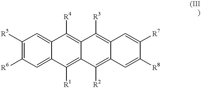
In formula (III), R1 to R4 represent substituted or unsubstituted alkyl, aryl, amino, heterocyclic or alkenyl groups, preferably aryl, amino, heterocyclic or alkenyl groups.
The aryl groups represented by R1 to R4 may be monocyclic or polycyclic and include fused rings and ring assemblies. Each aryl group preferably has 6 to 30 carbon atoms in total and may have a substituent or substituents. Preferred examples of the aryl groups represented by R1 to R4 include phenyl, o-, m- or p-tolyl, pyrenyl, perylenyl, coronenyl, 1- or 2-naphthyl, anthryl, o-, m- or p-biphenylyl, terphenyl and phenanthryl.
The amino groups represented by R1 to R4 may be alkylamino, arylamino or aralkylamino groups. These groups preferably have an aliphatic moiety of 1 to 6 carbon atoms in total and/or 1 to 4 aromatic carbocycles. Preferred examples of the amino groups include dimethylamino, diethylamino, dibutylamino, diphenylamino, ditolylamino, bisdiphenylylamino, and bisnaphthylamino groups.
The heterocyclic groups represented by R1 to R4 include 5- or 6-membered aromatic heterocyclic groups containing O, N or S as the hetero atom and fused polycyclic aromatic heterocyclic groups having 2 to 20 carbon atoms. Exemplary aromatic heterocyclic groups and fused polycyclic aromatic heterocyclic groups are thienyl, furyl, pyrrolyl, pyridyl, quinolyl, and quinoxalyl groups.
The alkenyl groups represented by R1 to R4 are preferably substituted alkenyl groups having a phenyl group as at least one of the substituents, for example, 1- or 2-phenylalkenyl, 1,2- or 2,2-diphenylalkenyl, and 1,2,2-triphenylalkenyl groups, although unsubstituted alkenyl groups are acceptable.
Where the R1 to R4 groups have substituents, it is preferred that at least two of the substituents are aryl, amino, heterocyclic, alkenyl or aryloxy groups. These aryl, amino, heterocyclic and alkenyl substituents are the same as defined for R1 to R4. The aryloxy substituents are preferably those having an aryl group of 6 to 18 carbon atoms in total, for example, o-, m- or p-phenoxy. It is also acceptable that at least two of the substituents form a fused ring. These substituents may further have substituents, examples of which are as described above.
Where the R1 to R4 groups have substituents, it is preferred that at least two of the substituents have the above-described substituents. The substituted position is not critical and may be any of ortho, meta and para-positions. It is preferred that R1 and R4 are identical and R2 and R3 are identical, although they may be different.
Preferably at least five, more preferably at least six of R1 to R8 are substituted or unsubstituted alkyl, aryl, amino, alkenyl or heterocyclic groups.
R5, R6, R7 and R8 are hydrogen or substituted or unsubstituted alkyl, aryl, amino or alkenyl groups.
The alkyl groups represented by R5 to R8 are preferably those of 1 to 6 carbon atoms, which may be straight or branched. Preferred examples of the alkyl groups are methyl, ethyl, n- and i-propyl, n-, i-, sec- and tert-butyl, and n-, i-, neo- and tert-pentyl.
The aryl, amino and alkenyl groups represented by R5 to R8 are as described for R1 to R4. It is preferred that R5 and R6 are identical and R7 and R8 are identical, although they may be different.
Also preferred are naphthacene compounds having a basic skeleton of the following formula (IV). 
In formula (IV), R11 to R13, R21 to R23, R31to R33, and R41 to R43 are hydrogen, aryl, amino, heterocyclic, aryloxy or alkenyl groups. Preferably at least one of R11 to R13, has a and aryloxy groups. At least two of R11 to R13 may form a fused ring. Where all of R11 to R13 are hydrogen, it is preferred that any one of R5, R6, R7 and R8 has an alkyl or aryl group. The same applies to each set of R21 to R23, R31 to R33, and R41 to R43.
Preferred examples of the aryl, amino, heterocyclic, and aryloxy groups are the same as described for R1 to R4 . It is preferred that R11 to R13 and R41 to R43 are identical and R21 to R23 and R31 to R33 are identical although they may be different.
The amino groups as the substituents on R11 to R13, R21 to R23, R31 to R33, and R41 to R43 may be alkylamino, arylamino or aralkylamino groups. These groups preferably have an aliphatic moiety of 1 to 6 carbon atoms in total and/or 1 to 4 aromatic carbocycles. Preferred examples of the amino groups include dimethylamino, diethylamino, dibutylamino, diphenylamino, ditolylamino, and bisdiphenylylamino groups.
Examples of the fused ring formed include indene, naphthalene, anthracene, phenanthrene, quinoline, isoquinoline, quinoxaline, phenazine, acridine, indole, carbazole, phenoxazine, phenothiazine, benzothiazole, benzothiophene, benzofuran, acridone, benzimidazole, coumarin, and flavone.
The buffer layer containing the porphyrin or naphthacene compound is formed by any well-known organic material depositing process such as evaporation. When the evaporation process is employed, the preferred conditions for vacuum evaporation include a vacuum of 10−4 Pa or lower and a deposition rate of about 0.01 to 1 nm/sec, though not critical. In vacuum, the buffer layer can be formed continuous to an organic layer (typically light emitting layer). It is preferred to successively form layers in vacuum because the successive formation in vacuum can avoid adsorption of impurities on the interface between the layers, thus ensuring better performance.
The buffer layer preferably has a thickness of 0.1 to 20 nm, more preferably 0.5 to 10 nm. If the thickness of the buffer layer exceeds this range, the electron injecting efficiency would decline or the porphyrin or naphthacene compound can reveal its own color.
After the buffer layer is deposited, the electron injecting electrode is deposited thereon.
The electron injecting electrode is preferably formed from materials having a low work function, for example, metal elements such as K, Li, Na, Mg, La, Ce, Ca, Sr, Ba, Al, Ag, In, Sn, Zn, and Zr, and binary or ternary alloys made of two or three such metal elements for stability improvement. Exemplary alloys are Ag—Mg (Ag: 0.1 to 50 at %), Al—Li (Li: 0.01 to 14 at %), In—Mg (Mg: 50 to 80 at %), and Al—Ca (Ca: 0.01 to 20 at %). Also useful are fluorides of alkali metals (such as Li, Na, K, Rb and Cs) such as LiF, NaF, KF, RbF and CsF, and oxides of these alkali metals such as Li2O, Na2O, K2O, Rb2O, and Cs2O. Peroxides, compound oxides, and halides (other than fluorides) of alkali metals may also be used as well as nitrides and salts of alkali metals. A thin film of such a material or a multilayer film of two or more materials may be used as the electron injecting electrode layer.
It is especially preferred that the electron injecting electrode be formed of an aluminum-lithium alloy. The Al—Li alloy has a lithium content of 0.4 to 14 at %. The lithium content is preferably 0.4 to less than 6.5 at %, more preferably 0.4 to less than 5 at %, further preferably 0.4 to 4.5 at %, further preferably 0.4 to 4 at %, and most preferably 0.4 to 3 at %. Alternatively, the lithium content is preferably 6.5 to 14 at %, and more preferably 7 to 12 at %. With too high lithium contents, the electron injecting electrode deposited therefrom would lack stability. The objects of the invention cannot be attained with too low lithium contents. It is preferred to set the lithium content relatively high in order to enhance the stability of output luminance whereas it is recommended to set the lithium content relatively low in order to enhance the stability of drive voltage.
In addition to Al and Li, the alloy may contain at least one of Cu, Mg, Zr, Fe, Si and O as an additive or incidental impurity, in an amount of less than about 5% by weight for each.
The electron injecting electrode can be formed of an aluminum-lithium alloy to a graded structure having a lithium concentration varying in a thickness direction through the film such that lithium is concentrated near its interface with the organic layer and aluminum is concentrated near the opposite surface. The graded concentration enables that lithium element having a low work function be present in a high concentration at the interface with the organic layer where the electron injecting function is needed and lithium element having a high reactivity be present in a low concentration at the opposite surface where there is a more possibility of contact with the ambient atmosphere. As a consequence, the electron injecting electrode is improved in stability while maintaining a high electron injecting efficiency.
The electron injecting electrode having a graded concentration of lithium element can be readily formed, preferably by controlling the sputtering pressure. Alternatively, the graded concentration can be achieved by using both an Al—Li alloy target and an Al metal target and individually controlling the respective deposition rates. Instead of providing such a continuously graded concentration, a film in which the concentration of lithium is changed discontinuously or stepwise may be deposited.
Preferably the electron injecting electrode is deposited by sputtering. The sputtering process used may be a high-frequency sputtering process using an RF power supply. However, a DC sputtering process is preferred because the control of a deposition rate is easy and any damage to the organic EL structure can be reduced.
When the electron injecting electrode is deposited by sputtering, its adhesion at the interface with the organic layer is improved due to a surface migration effect because the sputtered atoms and groups have relatively high kinetic energy, as compared with the evaporation process. Since a surface oxide layer can be removed by pre-sputtering or moisture and oxygen adsorbed on the interface with the organic layer can be removed by back sputtering, a clean electrode-organic layer interface or electrode can be formed, leading to the manufacture of an organic EL device of higher quality and stability. Even when a mixture of materials having largely different vapor pressures is used as the target, there arises only a minimum difference in composition between the target and the deposited film. The sputtering process eliminates any limit on material as given by a vapor pressure in the case of evaporation. As compared with the evaporation process, the sputtering process eliminates a need to feed the material for a long period of time and improves the uniformity of film thickness and quality. This is advantageous from the viewpoint of productivity.
The electron injecting electrode formed by sputtering is a dense film which minimizes the ingress of moisture therein and has a high chemical stability as compared with the evaporated, coarse film. This leads to the manufacture of an organic EL device with a high efficiency and long lifetime.
The sputtering gas is preferably under a pressure of 0.1 to 5 Pa during sputtering. By changing the pressure of the sputtering gas during deposition, an electron injecting electrode having a graded concentration of metal elements can be formed.
The sputtering gas may be an inert gas such as He, Ar, Xe or Kr or nitrogen (N2) as used in conventional sputtering apparatus. In the case of reactive sputtering, a reactive gas such as H2, O2, C2H4, and NH3 may be used in combination with the inert gas.
The DC sputtering apparatus preferably has a power of 0.1 to 10 W/cm2, especially 0.5 to 7 W/cm2. A deposition rate of 0.1 to 100 nm/min, especially 1 to 30 nm/min is preferred.
The electron injecting electrode formed by sputtering sometimes contains the inert gas such as He, Ar, Xe or Kr or nitrogen used as the sputtering gas. The content of these sputtering gas elements is usually less than about 20 at %, preferably less than about 10 at %. The sputtering gas elements can be detected by gas emission upon heating, fluorescent x-ray analysis or electron probe microanalysis (EPMA).
The electron injecting electrode thin film may have a sufficient thickness to effect electron injection, for example, a thickness of at least 0.1 nm, preferably at least 0.5 nm, more preferably at least 1 nm. Although the upper limit is not critical, the film thickness is typically about 1 to about 500 nm. On the electron injecting electrode, an auxiliary or protective electrode may be provided, if desired.
The auxiliary electrode may have at least a sufficient thickness to ensure efficient electron injection and prevent the ingress of moisture, oxygen and organic solvents, for example, a thickness of at least 50 nm, preferably at least 100 nm, more preferably 100 to 500 nm. A too thin auxiliary electrode layer would exert its effect little, lose a step coverage capability, and provide insufficient connection to a terminal electrode. If too thick, greater stresses are generated in the auxiliary electrode layer, undesirably accelerating the growth rate of dark spots.
For the auxiliary electrode, an appropriate material may be chosen in consideration of the material of the electron injecting electrode to be combined therewith. For example, low resistivity metals such as aluminum may be used when the electron injection efficiency is of importance. Metal compounds such as TiN may be used when sealing is of importance.
The thickness of the electron injecting electrode and the auxiliary electrode combined is usually about 50 to about 500 nm though it is not critical.
Disposed below the buffer layer (and adjacent to the substrate) is an organic layer participating in at least a light emitting function. The organic layer includes a light emitting layer which is a single thin film or a laminate film of two or more thin films each formed of an organic compound having at least a light emitting function.
The light emitting layer has the functions of injecting holes and electrons, transporting them, and recombining holes and electrons to create excitons. It is preferred that relatively electronically neutral compounds be used in the light emitting layer because electrons and holes can be easily injected and transported in a well balanced manner.
In addition to the light emitting layer of a strictly defined sense, the organic layer may further include a hole injecting and transporting layer, an electron injecting and transporting layer, etc.
The hole injecting and transporting layer has the functions of facilitating injection of holes from the hole injecting electrode, transporting holes stably, and obstructing electrons. The electron injecting and transporting layer has the functions of facilitating injection of electrons from the electron injecting electrode, transporting electrons stably, and obstructing holes. These layers are effective for increasing the number of holes and electrons injected into the light emitting layer and confining holes and electrons therein for optimizing the recombination region to improve light emission efficiency.
The thicknesses of the light emitting layer, the hole injecting and transporting layer, and the electron injecting and transporting layer are not critical and vary with a particular formation technique. Usually, their thickness is preferred to range from about 5 nm to about 500 nm, especially about 10 nm to about 300 nm.
The thickness of the hole injecting and transporting layer and the electron injecting and transporting layer is equal to or ranges from about 1/10 times to about 10 times the thickness of the light emitting layer although it depends on the design of a recombination/light emitting region. When the electron or hole injecting and transporting layer is divided into an injecting layer and a transporting layer, preferably the injecting layer is at least 1 nm thick and the transporting layer is at least 1 nm thick. The upper limit of thickness is usually about 500 nm for the injecting layer and about 500 nm for the transporting layer. The same film thickness applies when two injecting/transporting layers are provided.
The light emitting layer of the organic EL device contains a fluorescent material that is a compound having a light emitting capability. The fluorescent material may be at least one member selected from compounds as disclosed, for example, in JP-A 63-264692, such as quinacridone, rubrene, and styryl dyes. Also, quinoline derivatives such as metal complex dyes having 8-quinolinol or a derivative thereof as the ligand such as tris(8-quinolinolato)aluminum are included as well as tetraphenylbutadiene, anthracene, perylene, coronene, and 12-phthaloperinone derivatives. Further useful are the phenylanthracene derivatives described in JP-A 8-12600 and the tetraarylethene derivatives described in JP-A 8-12969.
It is preferred to use such a compound in combination with a host material capable of light emission by itself, that is, to use the compound as a dopant. In this embodiment, the content of the compound in the light emitting layer is preferably 0.01 to 10% by weight, especially 0.1 to 5% by weight. By using the compound in combination with the host material, the light emission wavelength of the host material can be altered, allowing light emission to be shifted to a longer wavelength and improving the luminous efficacy and stability of the device.
As the host material, quinolinolato complexes are preferable, with aluminum complexes having 8-quinolinol or a derivative thereof as the ligand being more preferable. These aluminum complexes are disclosed in JP-A 63-264692, 3-255190, 5-70733, 5-258859 and 6-215874.
Illustrative examples include tris(8-quinolinolato)-aluminum, bis(8-quinolinolato)magnesium, bis(benzo{f}-8-quinolinolato)zinc, bis(2-methyl-8-quinolinolato)aluminum oxide, tris(8-quinolinolato)indium, tris(5-methyl-8-quinolinolato)aluminum, 8-quinolinolatolithium, tris(5-chloro-8-quinolinolato)gallium, bis(5-chloro-8-quinolinolato)calcium, 5,7-dichloro-8-quinolinolatoaluminum, tris(5,7-dibromo-8-hydroxyquinolinolato)aluminum, and poly[zinc(II)-bis(8-hydroxy-5-quinolinyl)methane].
Also useful are aluminum complexes having another ligand in addition to 8-quinolinol or a derivative thereof. Examples include bis(2-methyl-8-quinolinolato)(phenolato)-aluminum(III), bis(2-methyl-8-quinolinolato)(ortho-cresolato)aluminum(III), bis(2-methyl-8-quinolinolato)(meta-cresolato)aluminum(III), bis(2-methyl-8-quinolinolato)(para-cresolato)aluminum(III), bis(2-methyl-8-quinolinolato)-(ortho-phenylphenolato)aluminum(III), bis(2-methyl-8-quinolinolato)(meta-phenylphenolato)aluminum(III), bis(2-methyl-8-quinolinolato)(para-phenylphenolato)aluminum(III), bis(2-methyl-8-quinolinolato)(2,3-dimethylphenolato)-aluminum(III), bis(2-methyl-8-quinolinolato)(2,6-dimethyl-phenolato)aluminum(III), bis(2-methyl-8-quinolinolato)(3,4-dimethylphenolato)aluminum(III), bis(2-methyl-8-quinolinolato)(3,5-dimethylphenolato)aluminum(III), bis(2-methyl-8-quinolinolato)(3,5-di-tert-butylphenolato)-aluminum(III), bis(2-methyl-8-quinolinolato)(2,6-diphenyl-phenolato)aluminum(III), bis(2-methyl-8-quinolinolato)-(2,4,6-triphenylphenolato)aluminum(III), bis(2-methyl-8-quinolinolato)(2,3,6-trimethylphenolato)aluminum(III), bis(2-methyl-8-quinolinolato)(2,3,5,6-tetramethylphenolato)-aluminum(III), bis(2-methyl-8-quinolinolato)(1-naphtholato)-aluminum(III), bis(2-methyl-8-quinolinolato)(2-naphtholato)-aluminum(III), bis(2,4-dimethyl-8-quinolinolato)(ortho-phenylphenolato)aluminum(III), bis(2,4-dimethyl-8-quinolinolato)(para-phenylphenolato)aluminum(III), bis(2,4-dimethyl-8-quinolinolato)(meta-phenylphenolato)aluminum(III), bis(2,4-dimethyl-8-quinolinolato)(3,5-dimethylphenolato)-aluminum(III), bis(2,4-dimethyl-8-quinolinolato)(3,5-di-tert-butylphenolato)aluminum(III), bis(2-methyl-4-ethyl-8-quinolinolato)(para-cresolato)aluminum(III), bis(2-methyl-4-methoxy-8-quinolinolato)(para-phenylphenolato)aluminum(III), bis(2-methyl-5-cyano-8-quinolinolato)(ortho-cresolato)-aluminum(III), and bis(2-methyl-6-trifluoromethyl-8-quinolinolato) (2-naphtholato)aluminum(III).
Also acceptable are bis(2-methyl-8-quinolinolato)-aluminum(III)-μ-oxo-bis(2-methyl-8-quinolinolato)aluminum(III), bis(2,4-dimethyl-8-quinolinolato)aluminum(III)-μ-oxo-bis(2,4-dimethyl-8-quinolinolato)aluminum(III), bis(4-ethyl-2-methyl-8-quinolinolato)aluminum(III)-μ-oxo-bis(4-ethyl-2-methyl-8-quinolinolato)aluminum(III), bis(2-methyl-4-methoxyquinolinolato)aluminum(III)-μ-oxo-bis(2-methyl-4-methoxyquinolinolato)aluminum(III), bis(5-cyano-2-methyl-8-quinolinolato)aluminum(III)-μ-oxo-bis(5-cyano-2-methyl-8-quinolinolato)aluminum(III), and bis(2-methyl-5-trifluoromethyl-8-quinolinolato)aluminum(III)-μ-oxo-bis(2-methyl-5-trifluoromethyl-8-quinolinolato)aluminum(III).
Other useful host materials are the phenylanthracene derivatives described in JP-A 8-12600 and the tetraarylethene derivatives described in JP-A 8-12969.
The light emitting layer may also serve as the electron transporting layer. In this case, tris(8-quinolinolato)aluminum etc. are preferably used. These fluorescent materials may be evaporated.
Also, if necessary, the light emitting layer may also be a layer of a mixture of at least one hole injecting and transporting compound and at least one electron injecting and transporting compound, to which a dopant is preferably added. In such a mix layer, the content of the dopant is preferably 0.01 to 20% by weight, especially 0.1 to 15% by weight.
In the mix layer, carrier hopping conduction paths are created, allowing carriers to move through a polarly predominant material while injection of carriers of opposite polarity is rather inhibited, and the organic compound becomes less susceptible to damage, resulting in the advantage of an extended device life. By incorporating the aforementioned dopant in such a mix layer, the light emission wavelength the mix layer itself possesses can be altered, allowing light emission to be shifted to a longer wavelength and improving the luminous intensity and stability of the device.
The hole injecting and transporting compound and electron injecting and transporting compound used in the mix layer may be selected from the following hole injecting and transporting compounds and electron injecting and transporting compounds, respectively.
The electron injecting and transporting compound is preferably selected from quinoline derivatives and metal complexes having 8-quinolinol or a derivative thereof as a ligand, especially tris(8-quinolinolato)aluminum (Alq3). The aforementioned phenylanthracene derivatives and tetraarylethene derivatives are also preferable.
For the hole injecting and transporting layer, amine derivatives having intense fluorescence are useful, for example, triphenyldiamine derivatives, styrylamine derivatives, and amine derivatives having an aromatic fused ring.
The mix ratio is preferably determined in accordance with the carrier density and carrier mobility. It is usually preferred that the weight ratio of the hole injecting and transporting compound to the electron injecting and transporting compound range from about 1/99 to about 99/1, more preferably from about 10/90 to about 90/10, especially from about 20/80 to about 80/20.
Also preferably, the thickness of the mix layer ranges from the thickness of a mono-molecular layer to less than the thickness of the organic compound layer, specifically from 1 to 100 nm, more preferably 5 to 60 nm, especially 5 to 50 nm.
Preferably the mix layer is formed by a co-deposition process of evaporating the compounds from distinct sources. If both the compounds have approximately equal or very close vapor pressures or evaporation temperatures, they may be pre-mixed in a common evaporation boat, from which they are evaporated together. The mix layer is preferably a uniform mixture of both the compounds although the compounds can be present in island form. The light emitting layer is generally formed to a predetermined thickness by evaporating an organic fluorescent material or coating a dispersion thereof in a resin binder.
As the hole injecting and transporting compound, there may be used various organic compounds as described, for example, in JP-A 63-295695, 2-191694, 3-792, 5-234681, 5-239455, 5-299174, 7-126225, 7-126226, and 8-100172, and EP 0650955A1. Exemplary are tetraarylbenzidine compounds (triaryldiamines or triphenyldiamines: TPD), aromatic tertiary amines, hydrazone derivatives, carbazole derivatives, triazole derivatives, imidazole derivatives, oxadiazole derivatives having an amino group, and polythiophenes. Two or more of these compounds may be used, and on such combined use, they may be formed as separate layers or mixed.
As the electron injecting and transporting compound, there may be used quinoline derivatives including organic metal complexes having 8-quinolinol or a derivative thereof as a ligand such as tris(8-quinolinolato)aluminum (Alq3), oxadiazole derivatives, perylene derivatives, pyridine derivatives, pyrimidine derivatives, quinoxaline derivatives, diphenylquinone derivatives, and nitro-substituted fluorene derivatives.
In forming the hole injecting and transporting layer, the light emitting layer, and the electron injecting and transporting layer, vacuum evaporation is preferably used because homogeneous thin films are available. By utilizing vacuum evaporation, there is obtained a homogeneous thin film which is amorphous or has a crystal grain size of less than 0.1 μm. If the grain size is more than 0.1 μm, uneven light emission would take place and the drive voltage of the device must be increased with a substantial drop of charge injection efficiency.
The conditions for vacuum evaporation are not critical although a vacuum of 10−4 Pa or lower and a deposition rate of about 0.01 to 1 nm/sec are preferred. It is preferred to successively form layers in vacuum because the successive formation in vacuum can avoid adsorption of impurities on the interface between the layers, thus ensuring better performance. Also, the drive voltage of a device can be reduced and the development and growth of dark spots be restrained.
In the embodiment wherein the respective layers are formed by vacuum evaporation, where it is desired for a single layer to contain two or more compounds, boats having the compounds received therein are individually temperature controlled to achieve co-deposition.
Further preferably, a shield plate may be provided on the device in order to prevent the organic layers and electrodes from deterioration. In order to prevent the ingress of moisture, the shield plate is attached to the substrate through an adhesive resin layer for sealing. The sealing or filler gas is preferably an inert gas such as argon, helium, and nitrogen. The filler gas should preferably have a moisture content of less than about 100 ppm, more preferably less than about 10 ppm, especially less than about 1 ppm. The lower limit of the moisture content is usually about 0.1 ppm though not critical.
The shield plate is selected from plates of transparent or translucent materials such as glass, quartz and resins, with glass being especially preferred. Alkali glass is preferred because of economy although other glass compositions such as soda lime glass, lead alkali glass, borosilicate glass, aluminosilicate glass, and silica glass are also useful. Of these, plates of soda glass without surface treatment are inexpensive and useful. Metal plates and plastic plates may also be used as the shield plate.
Using a spacer for height adjustment, the shield plate may be held at a desired height over the layer structure. The spacer may be formed from resin beads, silica beads, glass beads, and glass fibers, with the glass beads being especially preferred. Usually the spacer is formed from particles having a narrow particle size distribution while the shape of particles is not critical. Particles of any shape which does not obstruct the spacer function may be used. Preferred particles have an equivalent circle diameter of about 1 to 20 μm, more preferably about 1 to 10 μm, most preferably about 2 to 8 μm. Particles of such diameter should preferably have a length of less than about 100 μm. The lower limit of length is not critical although it is usually equal to or more than the diameter.
When a shield plate having a recess is used, the spacer may be used or not. When used, the spacer should preferably have a diameter in the above-described range, especially 2 to 8 μm.
The spacer may be premixed in a sealing adhesive or mixed with a sealing adhesive at the time of bonding. The content of the spacer in the sealing adhesive is preferably 0.01 to 30% by weight, more preferably 0.1 to 5% by weight.
Any adhesive which can maintain stable bond strength and gas tightness may be used although UV-curable epoxy resin adhesives of cation curing type are preferred.
The substrate on which the organic EL structure is formed may be selected from amorphous substrates of glass and quartz and crystalline substrates of Si, GaAs, ZnSe, ZnS, GaP, and InP, for example. If desired, buffer layers of crystalline materials, amorphous materials or metals may be formed on such crystalline substrates. Metal substrates including Mo, Al, Pt, Ir, Au and Pd are also useful. Of these, glass substrates are preferred. Since the substrate is often situated on the light exit side, the substrate should preferably have a light transmittance as described above for the electrode.
A plurality of inventive devices may be arrayed on a plane. A color display is obtained when the respective devices of a planar array differ in emission color.
The substrate may be provided with a color filter film, a fluorescent material-containing color conversion film or a dielectric reflecting film for controlling the color of light emission.
The color filter film used herein may be a color filter as used in liquid crystal displays and the like. The properties of a color filter may be adjusted in accordance with the light emission of the organic EL device so as to optimize the extraction efficiency and color purity.
It is also preferred to use a color filter capable of cutting external light of short wavelength which is otherwise absorbed by the EL device materials and fluorescence conversion layer, because the light resistance and display contrast of the device are improved. An optical thin film such as a multilayer dielectric film may be used instead of the color filter.
The fluorescence conversion filter film is to convert the color of light emission by absorbing electroluminescence and allowing the fluorescent material in the film to emit light. It is formed from three components: a binder, a fluorescent material, and a light absorbing material.
The fluorescent material used may basically have a high fluorescence quantum yield and desirably exhibits strong absorption in the EL wavelength region. In practice, laser dyes are appropriate. Use may be made of rhodamine compounds, perylene compounds, cyanine compounds, phthalocyanine compounds (including sub-phthalocyanines), naphthalimide compounds, fused ring hydrocarbon compounds, fused heterocyclic compounds, styryl compounds, and coumarin compounds.
The binder is selected from materials which do not cause extinction of fluorescence, preferably those materials which can be finely patterned by photolithography or printing technique. Also, where the filter film is formed on the substrate so as to be contiguous to the hole injecting electrode, those materials which are not damaged during deposition of the hole injecting electrode (such as ITO or IZO) are preferable.
The light absorbing material is used when the light absorption of the fluorescent material is short and may be omitted if unnecessary. The light absorbing material may also be selected from materials which do not cause extinction of fluorescence of the fluorescent material.
As shown in FIG. 1, the organic EL device of the invention may have the successively stacked configuration of substrate 1/hole injecting electrode 2/hole injecting and transporting layer 3/light emitting layer 4/buffer layer 6/electron injecting electrode 7. As shown in FIG. 2, the device may have the successively stacked configuration of substrate 1/hole injecting electrode 2/hole injecting and transporting layer 3/light emitting layer 4/electron injecting and transporting layer 5/buffer layer 6/electron injecting electrode 7. Among such configurations, a choice may be properly made in accordance with the desired characteristics and performance of the device, and a modification may be made if necessary. In the configurations of FIGS. 1 and 2, a drive power supply E is connected between the hole injecting electrode 2 and the electron injecting electrode 7.
The organic EL device of the invention is generally of the dc or pulse drive type while it can be of the ac drive type. The applied voltage is generally about 2 to 30 volts.
Examples of the invention are given below by way of illustration and not by way of limitation.
A substrate of (7059) glass by Corning Glass Works was scrubbed using a neutral detergent. The substrate was secured by a holder in a sputtering chamber which was evacuated to a vacuum. By DC magnetron sputtering from an ITO target, a hole injecting electrode of ITO having a thickness of 100 nm was formed on the substrate. The substrate having the patterned ITO electrode was subjected to ultrasonic washing with neutral detergent, acetone, and ethanol, pulled up from boiling ethanol, and dried. The surface was further cleaned with UV/ozone.
The substrate was secured by a holder in a vacuum evaporation chamber, which was evacuated to a vacuum of 1×10⁻⁴ Pa or lower. By an evaporation process, 4,4′,4″-tris(N-(3-methylphenyl)-N-phenylamino)triphenylamine (m-MTDATA) was evaporated at a deposition rate of 0.1 nm/sec to a thickness of 55 nm, forming a hole injecting layer. Then, N,N′-diphenyl-N,N′-m-tolyl-4,4′-diamino-1,1′-biphenyl (TPD) was evaporated at a deposition rate of 0.1 nm/sec to a thickness of 20 nm, forming a hole transporting layer. With the vacuum kept, tris(8-quinolinolato)aluminum (Alq3) was evaporated at a deposition rate of 0.1 nm/sec to a thickness of 50 nm, forming a light emitting layer. Next, copper phthalocyanine was evaporated at a deposition rate of 0.1 nm/sec to a thickness of 10 nm, forming a buffer layer (sample No. 1). Another sample (sample No. 2) was prepared by evaporating copper phthalocyanine to a thickness of 1 nm.
With the vacuum kept, by a sputtering process, AlLi (Li: 6 at %) was deposited to a thickness of 1 nm and Al was successively deposited to a thickness of 200 nm, forming an electron injecting electrode. Finally, a glass shield was sealed to the layer structure to complete an organic EL device.
For comparison purposes, an organic EL device (Comparative Sample) was similarly fabricated except that the buffer layer was omitted.
The organic EL device samples were measured for a light emission start voltage (that is, the voltage at which light emission was visually ascertainable), an output luminance at a constant current density of 10 mA/cm2, and a drive voltage. The results are shown in Table 1.
Sample No. 1 and Comparative Sample were subject to an accelerated test of continuously driving at a constant current density of 100 mA/cm2. The time passed until the development or growth of a dark spot having an equivalent circle diameter in excess of 100 μm was found was measured. The results are also shown in Table 1.
| TABLE 1 | ||||
| Time until | ||||
| Light emission | Drive | dark spot | ||
| start voltage | Luminance | voltage | development | |
| Sample | (V) | (cd/m2) | (V) | (hr.) |
| No. 1 | 2.7 | 660 | 5.1 | 400 |
| No. 2 | 3.5 | 580 | 6.0 | — |
| Comparison | 4.1 | 560 | 6.6 | 200 |
As evident from Table 1, the samples within the scope of the invention show a low initial emission voltage and a low drive voltage and subsequently develop minimal dark spots.
Organic EL devices were fabricated as in Example 1 except that the buffer layer was formed using phthalocyanine (free of the center metal). These devices were examined as in Example 1, finding equivalent results.
Organic EL devices were fabricated as in Example 1 except that the buffer layer was formed using rubrene (i.e., 5,6,11,12-tetraphenylnaphthacene). These devices were examined as in Example 1, finding equivalent results.
Organic EL devices were fabricated as in Example 1 except that the buffer layer was formed using 5,12-bis(biphenylyl)-6,11-diphenylnaphthacene. These devices were examined as in Example 1, finding equivalent results.
Equivalent results were obtained when the material of which the buffer layer was formed was replaced by 5,12-bis(2-naphthyl)-6,11-diphenylnaphthacene, 5,12-diphenyl-6,11-triphenylaminonaphthacene, 5,12-diphenyl-6,11-bis(triphenylethenyl)naphthacene, 2,3-dimethyl-5,6,11,12-tetraphenylnaphthacene, 2,3,5,6,11,12-hexaphenylnaphthacene, 6,11-bis(biphenylyl)-2,3,5,12-tetraphenylnaphthacene, and 5,12-bis(biphenylyl)-2,3,6,8,9,11-hexaphenylnaphthacene.
There have been described organic EL devices which can be manufactured without damages to organic layers, have a low initial drive voltage, a low emission start voltage, a high efficiency, and a long lifetime, and minimize the development of dark spots.
The invention has been described in detail with particular reference to preferred embodiments thereof, but it will be understood that variations and modifications can be effected within the spirit and scope of the invention.
Claims (8)
1. An organic electroluminescent device comprising
a substrate,
a hole injecting electrode and an electron injecting electrode on the substrate, said electron injecting electrode comprising a metal, metal oxide or metal halide,
an organic layer participating in at least a light emitting function disposed between the electrodes, and
a buffer layer comprising a naphthacene compound disposed between said organic layer and said electron injecting electrode.
2. The organic electroluminescent device of claim 1 wherein said electron injecting electrode is formed by sputtering and composed of an aluminum-lithium alloy containing 0.4 to 14 at % of lithium.
3. The organic electroluminescent device of claim 1 wherein said electron injecting electrode is formed by sputtering and contains 6.5 to 14 at % of lithium.
4. The organic electroluminescent device of claim 1 wherein said buffer layer has a thickness of 0.1 to 20 nm.
5. An organic electroluminescent device comprising
a substrate,
a hole injecting electrode and an electron injecting electrode on the substrate, said electron injecting electrode comprising a metal, metal oxide or metal halide,
an organic layer participating in at least a light emitting function disposed between the electrodes, and
a buffer layer comprising a porphyrin or naphthacene compound disposed between said organic layer and said electron injecting electrode,
wherein said electron injecting electrode is formed by sputtering and composed of an aluminum-lithium alloy containing 0.4 to 14 at % of lithium.
6. The organic electroluminescent device of claim 5 and wherein said electron injecting electrode is formed by sputtering and contains 6.5 to 14 at % of lithium.
7. The organic electroluminescent device of claim 5 wherein said buffer layer has a thickness of 0.1 to 20 nm.
8. The organic electroluminescent device of claim 5 wherein the aluminum lithium alloy is of a graded structure having a lithium concentration varying in a thickness direction through the film such that lithium is concentrated near its interface with the organic layer and aluminum is concentrated near the opposite surface.
Applications Claiming Priority (2)
| Application Number | Priority Date | Filing Date | Title |
|---|---|---|---|
| JP10-252057 | 1998-08-21 | ||
| JP25205798 | 1998-08-21 |
Publications (1)
| Publication Number | Publication Date |
|---|---|
| US6339290B1 true US6339290B1 (en) | 2002-01-15 |
Family
ID=17231973
Family Applications (1)
| Application Number | Title | Priority Date | Filing Date |
|---|---|---|---|
| US09/379,112 Expired - Fee Related US6339290B1 (en) | 1998-08-21 | 1999-08-23 | Organic electroluminescent device and making method |
Country Status (2)
| Country | Link |
|---|---|
| US (1) | US6339290B1 (en) |
| EP (1) | EP0982783A3 (en) |
Cited By (16)
| Publication number | Priority date | Publication date | Assignee | Title |
|---|---|---|---|---|
| US20030054199A1 (en) * | 2001-09-06 | 2003-03-20 | Lg Electronics Inc. | Organic electroluminescent device |
| US20040070337A1 (en) * | 2002-10-09 | 2004-04-15 | Goh Kee Siang | Light emitting diode based light source emitting collimated light |
| US20040097161A1 (en) * | 2001-03-22 | 2004-05-20 | James Gourlay | Method of creating an electroluminescent device |
| US20040124432A1 (en) * | 2002-12-25 | 2004-07-01 | Au Optronics Corp. | Organic light-emitting diode devices having reduced ambient-light reflection and method of making the same |
| US20040246432A1 (en) * | 2002-12-27 | 2004-12-09 | Kaoru Tsuchiya | Method of manufacturing a display device |
| US20050079381A1 (en) * | 2001-06-06 | 2005-04-14 | Yuji Hamada | Organic electroluminescene device and luminance material |
| US20050088082A1 (en) * | 2003-10-28 | 2005-04-28 | Sharp Kabushiki Kaisha | Organic electroluminescence device |
| US20050112405A1 (en) * | 2003-09-30 | 2005-05-26 | Yuji Hamada | Organic electroluminescent element |
| US20050123799A1 (en) * | 2003-09-30 | 2005-06-09 | Yuji Hamada | Luminescent material and organic electroluminescent device |
| US6984734B2 (en) | 2002-02-26 | 2006-01-10 | Board Of Regents, The University Of Texas System | Cyclo[n]pyrroles and methods thereto |
| US20060019116A1 (en) * | 2004-07-22 | 2006-01-26 | Eastman Kodak Company | White electroluminescent device with anthracene derivative host |
| US20080111481A1 (en) * | 2000-12-28 | 2008-05-15 | Semiconductor Energy Laboratory Co., Ltd. | Light Emitting Device and Method of Manufacturing the Same |
| CN100391025C (en) * | 2003-01-27 | 2008-05-28 | 友达光电股份有限公司 | Organic light-emitting diode having a breaker construction and method for making same |
| CN100466324C (en) * | 2002-09-30 | 2009-03-04 | 三洋电机株式会社 | Light-emitting component containing multiple luminous layer |
| CN1901243B (en) * | 2006-07-25 | 2010-08-11 | 清华大学 | Organic electroluminescence device |
| US11471694B2 (en) * | 2019-01-29 | 2022-10-18 | Sj Global Co., Ltd. | Plasma electrode pad for treatment of wounds and plasma treatment device |
Families Citing this family (5)
| Publication number | Priority date | Publication date | Assignee | Title |
|---|---|---|---|---|
| US6579629B1 (en) * | 2000-08-11 | 2003-06-17 | Eastman Kodak Company | Cathode layer in organic light-emitting diode devices |
| US6551725B2 (en) | 2001-02-28 | 2003-04-22 | Eastman Kodak Company | Inorganic buffer structure for organic light-emitting diode devices |
| US6797129B2 (en) | 2002-06-03 | 2004-09-28 | Eastman Kodak Company | Organic light-emitting device structure using metal cathode sputtering |
| US8241467B2 (en) | 2004-08-10 | 2012-08-14 | Global Oled Technology Llc | Making a cathode structure for OLEDs |
| TWI321966B (en) * | 2005-03-25 | 2010-03-11 | Au Optronics Corp | Organic electro-luminescence device and method of manufacturing the same |
Citations (12)
| Publication number | Priority date | Publication date | Assignee | Title |
|---|---|---|---|---|
| US3935031A (en) | 1973-05-07 | 1976-01-27 | New England Institute, Inc. | Photovoltaic cell with enhanced power output |
| US4356429A (en) | 1980-07-17 | 1982-10-26 | Eastman Kodak Company | Organic electroluminescent cell |
| US5458977A (en) | 1990-06-14 | 1995-10-17 | Idemitsu Kosan Co., Ltd. | Electroluminescence device containing a thin film electrode |
| EP0704915A1 (en) | 1994-09-27 | 1996-04-03 | Oki Electric Industry Co., Ltd. | Organic electroluminescent light-emitting array and optical head assembly |
| WO1998024272A1 (en) | 1996-11-27 | 1998-06-04 | Tdk Corporation | Organic el element |
| JPH10223372A (en) | 1997-02-10 | 1998-08-21 | Sony Corp | Organic electroluminescent element and flat panel display using it |
| JPH10321374A (en) | 1997-05-20 | 1998-12-04 | Tdk Corp | Organic el(electroluminescent)element |
| JPH1116681A (en) | 1997-04-30 | 1999-01-22 | Tdk Corp | Organic el element |
| WO1999020081A2 (en) | 1997-10-09 | 1999-04-22 | The Trustees Of Princeton University | Highly transparent non-metallic cathodes |
| EP0917216A2 (en) | 1997-11-17 | 1999-05-19 | Lg Electronics Inc. | Organic electroluminescent device with improved long-term stability |
| US5932363A (en) * | 1997-10-02 | 1999-08-03 | Xerox Corporation | Electroluminescent devices |
| EP0977287A2 (en) | 1998-07-28 | 2000-02-02 | Eastman Kodak Company | Interfacial electron-injecting layer formed from a doped cathode for organic light-emitting structure |
-
1999
- 1999-08-23 EP EP99306669A patent/EP0982783A3/en not_active Withdrawn
- 1999-08-23 US US09/379,112 patent/US6339290B1/en not_active Expired - Fee Related
Patent Citations (13)
| Publication number | Priority date | Publication date | Assignee | Title |
|---|---|---|---|---|
| US3935031A (en) | 1973-05-07 | 1976-01-27 | New England Institute, Inc. | Photovoltaic cell with enhanced power output |
| US4356429A (en) | 1980-07-17 | 1982-10-26 | Eastman Kodak Company | Organic electroluminescent cell |
| US5458977A (en) | 1990-06-14 | 1995-10-17 | Idemitsu Kosan Co., Ltd. | Electroluminescence device containing a thin film electrode |
| EP0704915A1 (en) | 1994-09-27 | 1996-04-03 | Oki Electric Industry Co., Ltd. | Organic electroluminescent light-emitting array and optical head assembly |
| WO1998024272A1 (en) | 1996-11-27 | 1998-06-04 | Tdk Corporation | Organic el element |
| JPH10223372A (en) | 1997-02-10 | 1998-08-21 | Sony Corp | Organic electroluminescent element and flat panel display using it |
| JPH1116681A (en) | 1997-04-30 | 1999-01-22 | Tdk Corp | Organic el element |
| JPH10321374A (en) | 1997-05-20 | 1998-12-04 | Tdk Corp | Organic el(electroluminescent)element |
| US5932363A (en) * | 1997-10-02 | 1999-08-03 | Xerox Corporation | Electroluminescent devices |
| WO1999020081A2 (en) | 1997-10-09 | 1999-04-22 | The Trustees Of Princeton University | Highly transparent non-metallic cathodes |
| EP0917216A2 (en) | 1997-11-17 | 1999-05-19 | Lg Electronics Inc. | Organic electroluminescent device with improved long-term stability |
| EP0977287A2 (en) | 1998-07-28 | 2000-02-02 | Eastman Kodak Company | Interfacial electron-injecting layer formed from a doped cathode for organic light-emitting structure |
| US6140763A (en) * | 1998-07-28 | 2000-10-31 | Eastman Kodak Company | Interfacial electron-injecting layer formed from a doped cathode for organic light-emitting structure |
Non-Patent Citations (2)
| Title |
|---|
| G. Parthasarathy, et al., Appl. Phys. Lett., vol. 72, No. 17, pp. 2138-2140, "A Metal-Free Cathode for Organic Semiconductor Devices", Apr. 27, 1998. |
| V. Bulovic, et al., Appl. Phys. Lett., vol. 70, No. 22, pp. 2954-2956, "A Surface-Emitting Vacuum-Deposited Organic Light Emitting Device", Jun. 2, 1997. |
Cited By (33)
| Publication number | Priority date | Publication date | Assignee | Title |
|---|---|---|---|---|
| US20080111481A1 (en) * | 2000-12-28 | 2008-05-15 | Semiconductor Energy Laboratory Co., Ltd. | Light Emitting Device and Method of Manufacturing the Same |
| US9362518B2 (en) | 2000-12-28 | 2016-06-07 | Semiconductor Energy Laboratory Co., Ltd. | Light emitting device and method of manufacturing the same |
| US9209418B2 (en) | 2000-12-28 | 2015-12-08 | Semiconductor Energy Laboratory Co., Ltd. | Light emitting device and method of manufacturing the same |
| US8878431B2 (en) | 2000-12-28 | 2014-11-04 | Semiconductor Energy Laboratory Co., Ltd. | Light emitting device and method of manufacturing the same |
| US8432094B2 (en) | 2000-12-28 | 2013-04-30 | Semiconductor Energy Laboratory Co., Ltd. | Light emitting device and method of manufacturing the same |
| US20110169400A1 (en) * | 2000-12-28 | 2011-07-14 | Semiconductor Energy Laboratory Co., Ltd. | Light Emitting Device and Method of Manufacturing the Same |
| US7915807B2 (en) * | 2000-12-28 | 2011-03-29 | Semiconductor Energy Laboratory Co., Ltd. | Light emitting device and method of manufacturing the same |
| US20040097161A1 (en) * | 2001-03-22 | 2004-05-20 | James Gourlay | Method of creating an electroluminescent device |
| US7595588B2 (en) | 2001-03-22 | 2009-09-29 | Microemissive Displays Limited | Electroluminescent device and method of making same |
| US7598666B2 (en) * | 2001-06-06 | 2009-10-06 | Sanyo Electric Co., Ltd. | Organic electroluminescent device and luminescent material |
| US20050079381A1 (en) * | 2001-06-06 | 2005-04-14 | Yuji Hamada | Organic electroluminescene device and luminance material |
| US6844090B2 (en) * | 2001-09-06 | 2005-01-18 | Lg Electronics Inc. | Organic electroluminescent device |
| US20050042476A1 (en) * | 2001-09-06 | 2005-02-24 | Lg Electronics, Inc. | Organic electroluminescent device |
| US20030054199A1 (en) * | 2001-09-06 | 2003-03-20 | Lg Electronics Inc. | Organic electroluminescent device |
| US6984463B2 (en) | 2001-09-06 | 2006-01-10 | Lg Electronics Inc. | Organic electroluminescent device |
| US6984734B2 (en) | 2002-02-26 | 2006-01-10 | Board Of Regents, The University Of Texas System | Cyclo[n]pyrroles and methods thereto |
| CN100466324C (en) * | 2002-09-30 | 2009-03-04 | 三洋电机株式会社 | Light-emitting component containing multiple luminous layer |
| US7112916B2 (en) * | 2002-10-09 | 2006-09-26 | Kee Siang Goh | Light emitting diode based light source emitting collimated light |
| US20040070337A1 (en) * | 2002-10-09 | 2004-04-15 | Goh Kee Siang | Light emitting diode based light source emitting collimated light |
| US20040124432A1 (en) * | 2002-12-25 | 2004-07-01 | Au Optronics Corp. | Organic light-emitting diode devices having reduced ambient-light reflection and method of making the same |
| US6989280B2 (en) * | 2002-12-25 | 2006-01-24 | Au Optronics Corp. | Organic light-emitting diode devices having reduced ambient-light reflection and method of making the same |
| US20050139849A1 (en) * | 2002-12-25 | 2005-06-30 | Au Optronics Corp. | Organic light-emitting diode devices having reduced ambient-light reflection and method of making the same |
| US6876018B2 (en) * | 2002-12-25 | 2005-04-05 | Au Optronics, Corp. | Organic light-emitting diode devices having reduced ambient-light reflection and method of making the same |
| US7452257B2 (en) * | 2002-12-27 | 2008-11-18 | Semiconductor Energy Laboratory Co., Ltd. | Method of manufacturing a display device |
| US20040246432A1 (en) * | 2002-12-27 | 2004-12-09 | Kaoru Tsuchiya | Method of manufacturing a display device |
| CN100391025C (en) * | 2003-01-27 | 2008-05-28 | 友达光电股份有限公司 | Organic light-emitting diode having a breaker construction and method for making same |
| US20050112405A1 (en) * | 2003-09-30 | 2005-05-26 | Yuji Hamada | Organic electroluminescent element |
| US20050123799A1 (en) * | 2003-09-30 | 2005-06-09 | Yuji Hamada | Luminescent material and organic electroluminescent device |
| US7429822B2 (en) | 2003-10-28 | 2008-09-30 | Sharp Kabushiki Kaisha | Organic electroluminescence device having a cathode with a metal layer that includes a first metal and a low work function metal |
| US20050088082A1 (en) * | 2003-10-28 | 2005-04-28 | Sharp Kabushiki Kaisha | Organic electroluminescence device |
| US20060019116A1 (en) * | 2004-07-22 | 2006-01-26 | Eastman Kodak Company | White electroluminescent device with anthracene derivative host |
| CN1901243B (en) * | 2006-07-25 | 2010-08-11 | 清华大学 | Organic electroluminescence device |
| US11471694B2 (en) * | 2019-01-29 | 2022-10-18 | Sj Global Co., Ltd. | Plasma electrode pad for treatment of wounds and plasma treatment device |
Also Published As
| Publication number | Publication date |
|---|---|
| EP0982783A3 (en) | 2000-11-08 |
| EP0982783A2 (en) | 2000-03-01 |
Similar Documents
| Publication | Publication Date | Title |
|---|---|---|
| US6339290B1 (en) | Organic electroluminescent device and making method | |
| US6333521B1 (en) | Oleds containing thermally stable glassy organic hole transporting materials | |
| EP2220701B1 (en) | White oled with blue light-emitting layers | |
| US6469437B1 (en) | Highly transparent organic light emitting device employing a non-metallic cathode | |
| US6188176B1 (en) | Organic electroluminescent device and preparation method with ITO electrode (111) orientation | |
| US6451455B1 (en) | Metal complexes bearing both electron transporting and hole transporting moieties | |
| US6458475B1 (en) | Organic light emitting diode having a blue phosphorescent molecule as an emitter | |
| US6200695B1 (en) | Organic electroluminescent device | |
| US6284342B1 (en) | Organic EL display assembly | |
| US6333065B1 (en) | Process for the production of an organic electroluminescent device | |
| US6387544B1 (en) | OLEDS containing thermally stable glassy organic hole transporting materials | |
| JP2002367784A (en) | Organic el element | |
| EP0999256A1 (en) | Compounds for organic el element and organic el element | |
| US20020011782A1 (en) | Organic electroluminescent device with improved hole injecting structure | |
| EP1022788A2 (en) | Organic electroluminescent device | |
| EP1020938A2 (en) | Organic electroluminescent device | |
| US6252246B1 (en) | Organic electroluminescent device | |
| EP1022789A2 (en) | Organic electroluminescent device | |
| US6222314B1 (en) | Organic electoluminescent device with inorganic insulating hole injecting layer | |
| JP2001110571A (en) | Organic field light emitting element | |
| EP1041654A1 (en) | Organic electroluminescent device | |
| US6359384B1 (en) | Organic electroluminescent device with electron injecting electrode containing ALLi alloy | |
| EP0892587A2 (en) | Organic EL device and method for production thereof | |
| KR20010051823A (en) | Organic Electroluminescent Display Device | |
| JPH10335066A (en) | Organic electroluminescent element and flat panel display using this organic electroluminescent element |
Legal Events
| Date | Code | Title | Description |
|---|---|---|---|
| AS | Assignment |
Owner name: TDK CORPORATION, JAPAN Free format text: ASSIGNMENT OF ASSIGNORS INTEREST;ASSIGNOR:NAKAYA, KENJI;REEL/FRAME:011250/0582 Effective date: 19990805 |
|
| FPAY | Fee payment |
Year of fee payment: 4 |
|
| REMI | Maintenance fee reminder mailed | ||
| LAPS | Lapse for failure to pay maintenance fees | ||
| STCH | Information on status: patent discontinuation |
Free format text: PATENT EXPIRED DUE TO NONPAYMENT OF MAINTENANCE FEES UNDER 37 CFR 1.362 |
|
| FP | Lapsed due to failure to pay maintenance fee |
Effective date: 20100115 |