US6339486B1 - Holographic technique for illumination of image displays using ambient illumination - Google Patents
Holographic technique for illumination of image displays using ambient illumination Download PDFInfo
- Publication number
- US6339486B1 US6339486B1 US09/419,273 US41927399A US6339486B1 US 6339486 B1 US6339486 B1 US 6339486B1 US 41927399 A US41927399 A US 41927399A US 6339486 B1 US6339486 B1 US 6339486B1
- Authority
- US
- United States
- Prior art keywords
- optical element
- holographic optical
- holographic
- pair
- electrically conductive
- Prior art date
- Legal status (The legal status is an assumption and is not a legal conclusion. Google has not performed a legal analysis and makes no representation as to the accuracy of the status listed.)
- Expired - Fee Related
Links
Images


Classifications
-
- G—PHYSICS
- G02—OPTICS
- G02F—OPTICAL DEVICES OR ARRANGEMENTS FOR THE CONTROL OF LIGHT BY MODIFICATION OF THE OPTICAL PROPERTIES OF THE MEDIA OF THE ELEMENTS INVOLVED THEREIN; NON-LINEAR OPTICS; FREQUENCY-CHANGING OF LIGHT; OPTICAL LOGIC ELEMENTS; OPTICAL ANALOGUE/DIGITAL CONVERTERS
- G02F1/00—Devices or arrangements for the control of the intensity, colour, phase, polarisation or direction of light arriving from an independent light source, e.g. switching, gating or modulating; Non-linear optics
- G02F1/01—Devices or arrangements for the control of the intensity, colour, phase, polarisation or direction of light arriving from an independent light source, e.g. switching, gating or modulating; Non-linear optics for the control of the intensity, phase, polarisation or colour
- G02F1/13—Devices or arrangements for the control of the intensity, colour, phase, polarisation or direction of light arriving from an independent light source, e.g. switching, gating or modulating; Non-linear optics for the control of the intensity, phase, polarisation or colour based on liquid crystals, e.g. single liquid crystal display cells
- G02F1/133—Constructional arrangements; Operation of liquid crystal cells; Circuit arrangements
- G02F1/1333—Constructional arrangements; Manufacturing methods
- G02F1/1335—Structural association of cells with optical devices, e.g. polarisers or reflectors
- G02F1/1336—Illuminating devices
- G02F1/13362—Illuminating devices providing polarized light, e.g. by converting a polarisation component into another one
-
- G—PHYSICS
- G02—OPTICS
- G02B—OPTICAL ELEMENTS, SYSTEMS OR APPARATUS
- G02B30/00—Optical systems or apparatus for producing three-dimensional [3D] effects, e.g. stereoscopic images
- G02B30/50—Optical systems or apparatus for producing three-dimensional [3D] effects, e.g. stereoscopic images the image being built up from image elements distributed over a 3D volume, e.g. voxels
- G02B30/52—Optical systems or apparatus for producing three-dimensional [3D] effects, e.g. stereoscopic images the image being built up from image elements distributed over a 3D volume, e.g. voxels the 3D volume being constructed from a stack or sequence of 2D planes, e.g. depth sampling systems
-
- G—PHYSICS
- G02—OPTICS
- G02B—OPTICAL ELEMENTS, SYSTEMS OR APPARATUS
- G02B5/00—Optical elements other than lenses
- G02B5/32—Holograms used as optical elements
-
- G—PHYSICS
- G02—OPTICS
- G02F—OPTICAL DEVICES OR ARRANGEMENTS FOR THE CONTROL OF LIGHT BY MODIFICATION OF THE OPTICAL PROPERTIES OF THE MEDIA OF THE ELEMENTS INVOLVED THEREIN; NON-LINEAR OPTICS; FREQUENCY-CHANGING OF LIGHT; OPTICAL LOGIC ELEMENTS; OPTICAL ANALOGUE/DIGITAL CONVERTERS
- G02F1/00—Devices or arrangements for the control of the intensity, colour, phase, polarisation or direction of light arriving from an independent light source, e.g. switching, gating or modulating; Non-linear optics
- G02F1/01—Devices or arrangements for the control of the intensity, colour, phase, polarisation or direction of light arriving from an independent light source, e.g. switching, gating or modulating; Non-linear optics for the control of the intensity, phase, polarisation or colour
- G02F1/13—Devices or arrangements for the control of the intensity, colour, phase, polarisation or direction of light arriving from an independent light source, e.g. switching, gating or modulating; Non-linear optics for the control of the intensity, phase, polarisation or colour based on liquid crystals, e.g. single liquid crystal display cells
- G02F1/133—Constructional arrangements; Operation of liquid crystal cells; Circuit arrangements
- G02F1/1333—Constructional arrangements; Manufacturing methods
- G02F1/1335—Structural association of cells with optical devices, e.g. polarisers or reflectors
- G02F1/1336—Illuminating devices
- G02F1/133621—Illuminating devices providing coloured light
-
- G—PHYSICS
- G02—OPTICS
- G02F—OPTICAL DEVICES OR ARRANGEMENTS FOR THE CONTROL OF LIGHT BY MODIFICATION OF THE OPTICAL PROPERTIES OF THE MEDIA OF THE ELEMENTS INVOLVED THEREIN; NON-LINEAR OPTICS; FREQUENCY-CHANGING OF LIGHT; OPTICAL LOGIC ELEMENTS; OPTICAL ANALOGUE/DIGITAL CONVERTERS
- G02F1/00—Devices or arrangements for the control of the intensity, colour, phase, polarisation or direction of light arriving from an independent light source, e.g. switching, gating or modulating; Non-linear optics
- G02F1/01—Devices or arrangements for the control of the intensity, colour, phase, polarisation or direction of light arriving from an independent light source, e.g. switching, gating or modulating; Non-linear optics for the control of the intensity, phase, polarisation or colour
- G02F1/13—Devices or arrangements for the control of the intensity, colour, phase, polarisation or direction of light arriving from an independent light source, e.g. switching, gating or modulating; Non-linear optics for the control of the intensity, phase, polarisation or colour based on liquid crystals, e.g. single liquid crystal display cells
- G02F1/133—Constructional arrangements; Operation of liquid crystal cells; Circuit arrangements
- G02F1/1333—Constructional arrangements; Manufacturing methods
- G02F1/1334—Constructional arrangements; Manufacturing methods based on polymer dispersed liquid crystals, e.g. microencapsulated liquid crystals
- G02F1/13342—Holographic polymer dispersed liquid crystals
Definitions
- the present invention generally relates to illumination of image displays, and more particularly to illumination of image displays using holographic techniques.
- the present invention relates to an apparatus and method for illuminating an image display using ambient light.
- the present invention employs holographic techniques for collecting ambient light over a hemispherical region and redirecting the collective light into useful viewing directions.
- the apparatus of the present invention comprises at least a first pair of holographic optical elements each having a first surface aligned on a common axis.
- the first pair of holographic optical elements are themselves positioned such that the first surfaces of each face each other.
- the first holographic optical element of the first pair is configured to diffract a select portion of received ambient light. More particularly, the first holographic optical element is configured to diffract ambient light within a first bandwidth.
- the second optical element of the first pair is likewise configured to diffract a select portion of light received thereon. More particularly, the second holographic optical element is configured to diffract first bandwidth light which is received on the first surface thereof.
- first and second holographic optical elements are also configured to transmit light, other than the first bandwidth light, without substantial alteration.
- a quarter wave plate is positioned between and aligned with the first surfaces of the first and second optical elements.
- the second holographic optical element is switchable between active and inactive states.
- the second holographic optical element transmits first bandwidth light substantially unaltered when operating in its inactive state.
- the second holographic optical element diffracts first bandwidth light received on the first surface when operating in the active state.
- the first holographic optical element is switchable between active and inactive states. In the inactive state, the first holographic optical element is configured to transmit first bandwidth light substantially unaltered. In the active state, the first holographic optical element diffracts first bandwidth light.
- the first or second holographic optical element is formed from polymer dispersed liquid crystal material.
- the polymer dispersed liquid crystal material undergoes phase separation during the hologram recording process, creating regions densely populated by liquid crystal micro-droplets, interspersed by regions of clear photopolymer.
- the second holographic optical element comprises a layer of material that records a hologram and an array of electrically conductive elements, wherein the array of electrically conductive elements is positioned adjacent the layer of material that records the hologram.
- FIG. 1 is a cross-sectional of an electrically switchable hologram made of an exposed polymer dispersed liquid crystal (PDLC) material made in accordance with the teachings of the description herein;
- PDLC polymer dispersed liquid crystal
- FIG. 2 is a graph of the normalized net transmittance and normalized net diffraction efficiency of a hologram made in accordance with the teachings of the description herein (without the addition of a surfactant) versus the rms voltage applied across the hologram;
- FIG. 3 is a graph of both the threshold and complete switching rms voltages needed for switching a hologram made in accordance with the teachings of the description herein to minimum diffraction efficiency versus the frequency of the rms voltage;
- FIG. 4 is a graph of the normalized diffraction efficiency as a function of the applied electric field a PDLC material formed with 34% by weight liquid crystal surfactant present and a PDLC material formed with 29% by weight liquid crystal and 4% by weight surfactant;
- FIG. 5 is a graph showing the switching response time data for the diffracted beam in the surfactant-containing PDLC material in FIG. 4;
- FIG. 6 is a graph of the normalized net transmittance and the normalized net diffraction efficiency a hologram
- FIG. 7 is an elevation view of typical experimental arrangement for recording reflection gratings
- FIGS. 8 a and 8 b are elevational views of a reflection grating, made in accordance with the teachings of the description herein, having periodic planes of polymer channels and PDLC channels disposed parallel to the front surface in the absence of a field (FIG. 8 a ) and with an electric field applied (FIG. 8 b ) wherein the liquid-crystal utilized in the formation of the grating has a positive dielectric anisotropy;
- FIGS. 9 a and 9 b are elevational views of a reflection grating, made in accordance with the teachings of the description herein, having periodic planes of polymer channels and channels disposed parallel to the front surface of the grating in the absence of an electric field (FIG. 9 a ) and with an electric field applied (FIG. 9 b ) wherein the liquid crystal utilized in the formation of the grating has a negative dielectric anisotropy;
- FIG. 10 a is an elevational view of a reflection grating, made in accordance with the teachings of the description herein, disposed within a magnetic field generated by Helmholtz coils;
- FIGS. 10 b and 10 c are elevational views of the reflection grating of FIG. 10 a in the absence of an electric field (FIG. 10 b ) and with an electric field applied (FIG. 10 c );
- FIGS. 11 a and 11 b are representative side views of a slanted transmission grating (FIG. 11 a ) and a slanted reflection grating (FIG. 11 b ) showing the orientation of the grating vector G of the periodic planes of polymer channels and PDLC channels;
- FIG. 12 is an elevational view of a reflection grating, made in accordance with the teachings of the description herein, when a shear stress field is applied thereto;
- FIG. 13 is an elevational view of a subwavelength grating, made in accordance with the teachings of the description herein, having periodic planes of polymer channels and PDLC channels disposed perpendicular to the front surface of the grating;
- FIG. 14 a is an elevational view of a switchable subwavelength, made in accordance with the teachings of the description herein, wherein the subwavelength grating functions as a half wave plate whereby the polarization of the incident radiation is rotated by 90°;
- FIG. 14 b is an elevational view of the switchable half wave plate shown in FIG. 14 a disposed between crossed polarizers whereby the incident light is transmitted;
- FIGS. 14 c and 14 d are side views of the switchable half wave plate and crossed polarizes shown in FIG. 14 b and showing the effect of the application of a voltage to the plate where the polarization of the light is no longer rotated and thus blocked by the second polarizer;
- FIG. 15 a is a side view of a switchable subwavelength grating, made in accordance with the teachings of the description herein, wherein the subwavelength grating functions as a quarter wave plate whereby plane polarized light is transmitted through the subwavelength grating, retroreflected by a mirror and reflected by the beam splitter;
- FIG. 15 b is a side view of the switchable subwavelength grating of FIG. 15 a and showing the effect of the application of a voltage to the plate whereby the polarization of the light is no longer modified, thereby permitting the reflected light to pass through the beam splitter;
- FIGS. 16 a and 16 b are elevational views of a transmission grating, made in accordance with the teachings of the description herein, having periodic planes of polymer channels and PDLC channels disposed perpendicular to the front face of the grating in the absence of an electric field (FIG. 16 a ) and with an electric field applied (FIG. 16 b ) wherein the liquid crystal utilized in formation of the grating has a positive dielectric anisotropy;
- FIG. 17 is a side view of five subwavelength gratings wherein the gratings are stacked and connected electrically in parallel thereby reducing the switching voltage of the subwavelength grating;
- FIG. 18 a is block diagram of an optical system for illuminating conventional display devices such as flat panel displays in accordance with one embodiment of the present invention
- FIG. 18 b is a block diagram of an optical system for illuminating a diffractive display system in accordance with one embodiment of the present invention.
- FIG. 19 a is a cross-sectional view of one embodiment of a switchable holographic optical element employed in the systems shown in FIGS. 18 a and 18 b;
- FIG. 19 b is a cross-sectional view of one embodiment of the diffractive display employed in the system of FIG. 18 b;
- FIG. 20 is a diagram showing one embodiment of a holographic optical element employed in the diffractive display of FIG. 18 b
- FIGS. 21 a - 21 c a block diagrams showing operational aspects of one embodiment of the optical system shown in FIG. 18 a;
- FIGS. 22 a - 22 c are block diagrams showing operational aspects of the optical system and diffractive display system shown in FIG. 18 b;
- FIG. 23 is a graph showing the relation between emergence or diffracted angle and angle of incidence for a thin phase hologram.
- the present invention employs holographic optical elements formed, in one embodiment, from a polymer dispersed liquid crystal (PDLC) material comprising a monomer, a dispersed liquid crystal, a cross-linking monomer, a co-initiator and a photo-initiator dye.
- PDLC polymer dispersed liquid crystal
- These PDLC materials exhibit clear and orderly separation of the liquid crystal and cured polymer, whereby the PDLC material advantageously provides high quality optical elements.
- the PDLC materials used in the holographic optical elements may be formed in a single step.
- the holographic optical elements may also use a unique photopolymerizable prepolymer material that permits in situ control over characteristics of resulting gratings, such as domain size, shape, density, ordering and the like.
- methods and materials taught herein can be used to prepare PDLC materials for optical elements comprising switchable transmission or reflection type holographic gratings.
- a hologram for use in one embodiment of the present invention may be formed is controlled primarily by the choice of components used to prepare the homogeneous starting mixture, and to a lesser extent by the intensity of the incident light pattern.
- PDLC polymer dispersed liquid crystal
- a feature of one embodiment of PDLC material is that illumination by an inhomogeneous, coherent light pattern initiates a patterned, anisotropic diffusion (or counter diffusion) of polymerizable monomer and second phase material, particularly liquid crystal (LC).
- LC liquid crystal
- the resulting embodiment of PDLC material may have an anisotropic spatial distribution of phase-separated LC droplets within the photochemically cured polymer matrix.
- Prior art PDLC materials made by a single-step process can achieve at best only regions of larger LC bubbles and smaller LC bubbles in a polymer matrix.
- the large bubble sizes are highly scattering which produces a hazy appearance and multiple ordering diffractions, in contrast to the well-defined first order diffraction and zero order diffraction made possible by the small LC bubbles of one embodiment of PDLC material in well-defined channels of LC-rich material.
- the same may be prepared by coating the mixture between two indium-tin-oxide (ITO) coated glass slides separated by spacers of nominally 10-20 ⁇ m thickness.
- ITO indium-tin-oxide
- the sample is placed in a conventional holographic recording setup.
- Gratings are typically recorded using the 488 nm line of an Argon ion laser with intensities of between about 0.1-100 mW/cm 2 and typical exposure times of 30-120 seconds.
- the angle between the two beams is varied to vary the spacing of the intensity peaks, and hence the resulting grating spacing of the hologram. Photopolymerization is induced by the optical intensity pattern.
- the features of the PDLC material are influenced by the components used in the preparation of the homogeneous starting mixture and, to a lesser extent, by the intensity of the incident light pattern.
- the prepolymer material comprises a mixture of a photopolymerizable monomer, a second phase material, a photo-initiator dye, a co-initiator, a chain extender (or cross-linker), and, optionally, a surfactant.
- two major components of the prepolymer mixture are the polymerizable monomer and the second phase material, which are preferably completely miscible.
- Highly functionalized monomers may be preferred because they form densely cross-linked networks which shrink to some extent and to end to squeeze out the second phase material. As a result, the second phase material is moved anisotropically out of the polymer region and, thereby, separated into well-defined polymer-poor, second phase-rich regions or domains.
- Highly functionalized monomers may also be preferred because the extensive cross-linking associated with such monomers yields fast kinetics, allowing the hologram to form relatively quickly, whereby the second phase material will exist in domains of less than approximately 0.1 ⁇ m.
- Suitable acrylates such as triethyleneglycol diacrylate, trimethylolpropane triacrylate, pentaerythritol triacrylate, pentaerythritol tetracrylate, pentaerythritol pentacrylate, and the like can be used in the present invention.
- an approximately 1:4 mixture of tri-to penta-acrylate facilitates homogeneous mixing while providing a favorable mixture for forming 10-20 ⁇ m films on the optical plates.
- the second phase material of choice for use in the practice of the present invention is a liquid crystal (LC).
- LC liquid crystal
- the concentration of LC employed should be large enough to allow a significant phase separation to occur in the cured sample, but not so large as to make the sample opaque or very hazy. Below about 20% by weight very little phase separation occurs and diffraction efficiencies are low. Above about 35% by weight, the sample becomes highly scattering, reducing both diffraction efficiency and transmission. Samples fabricated with approximately 25% by weight typically yield good diffraction efficiency and optical clarity. In prepolymer mixtures utilizing a surfactant, the concentration of LC may be increased to 35% by weight without loss in optical performance by adjusting the quantity of surfactant.
- Suitable liquid crystals contemplated for use in the practice of the present invention may include the mixture of cyanobiphenyls marketed as E7 by Merck, 4′-n-pentyl-4-cyanobiphenyl, 4′-n-heptyl-4-cyanobiphenyl, 4′-octaoxy-4-cyanobiphenyl, 4′-pentyl-4-cyanoterphenyl, ⁇ -methoxybenzylidene-4′-butylaniline, and the like.
- Other second phase components are also possible.
- the polymer dispersed liquid crystal material employed in the practice of the present invention may be formed from a prepolymer material that is a homogeneous mixture of a polymerizable monomer comprising dipentaerythritol hydroxypentacrylate (available, for example, from Polysciences, Inc., Warrington, Pennsylvania), approximately 10-40 wt % of the liquid crystal E7 (which is a mixture of cyanobiphenyls marketed as E7 by Merck and also available from BDH Chemicals, Ltd., London, England), the chain-extending monomer N-vinylp-yrrolidinone (“NVP”) (available from the Aldrich Chemical Company, Milwaukee, Wis.), co-initiator N-phenylglycine (“NPG”) (also available from the Aldrich Chemical Company, Milwaukee, Wis.), and the photo-initiator dye rose bengal ester; (2,4,5,7-tetraiodo-3′,4′, 5′,6′-tetrachlor
- the mixture of liquid crystal and prepolymer material are homogenized to a viscous solution by suitable means (e.g., ultrasonification) and spread between indiumtin-oxide (ITO) coated glass sides with spacers of nominally 15-100 ⁇ m thickness and, preferably, 10-20 ⁇ m thickness.
- ITO indiumtin-oxide
- the ITO is electrically conductive and serves as an optically transparent electrode.
- Preparation, mixing and transfer of the prepolymer material onto the glass slides are preferably done in the dark, as the mixture is extremely sensitive to light.
- the sensitivity of the prepolymer materials to light intensity is dependent on the photo-initiator dye and its concentration.
- a higher dye concentration leads to a higher sensitivity.
- the solubility of the photo-initiator dye limits the concentration of the dye and, thus, the sensitivity of the prepolymer material.
- photoinitiator dye concentrations in the range of 0.2-0.4% by weight are sufficient to achieve desirable sensitivities and allow for a complete bleaching of the dye in the recording process, resulting in colorless final samples.
- Photo-initiator dyes that may be useful in generating PDLC materials are rose bengal ester (2,4,5,7-tetraiodo-3′,4′,5′, 6′-tetrachlorofluorescein-6-acetate ester); rose bengal sodium salt; eosin; eosin sodium salt; 4,5-diiodosuccinyl fluorescein; camphorquinone; methylene blue, and the like. These dyes allow a sensitivity to recording wavelengths across the visible spectrum from nominally 400 nm to 700 nm.
- Suitable near-infrared dyes such as cationic cyanine dyes with trialkylborate anions having absorption from 600-900 nm as well as merocyanine dyes derived from spiropyran may also find utility in the present invention.
- the co-initiator employed in the practice of the present invention controls the rate of curing in the free radical polymerization reaction of the prepolymer material. Optimum phase separation and, thus, optimum diffraction efficiency in the resulting PDLC material, are a function of curing rate. It has been found that favorable results can be achieved utilizing co-initiator in the range of 2-3% by weight.
- Suitable co-initiators include N-phenylglycine; triethyl amine; triethanolamine; N,N-dimethyl-2,6-diisopropyl aniline, and the like.
- Suitable dyes and dye co-initiator combinations that may be suitable for use in the present invention, particularly for visible light, include eosin and triethanolamine; camphorquinone and N-phenylglycine; fluorescein and triethanolamine; methylene blue and triethanolamine or N-phenylglycine; erythrosin B and triethanolamine; indolinocarbocyanine and triphenyl borate; iodobenzospiropyran and triethylamine, and the like.
- the chain extender (or cross linker) employed in the practice of the present invention may help to increase the solubility of the components in the prepolymer material as well as increase the speed of polymerization.
- the chain extender is preferably a smaller vinyl monomer as compared with the pentacrylate, whereby it can react with the acrylate positions in the pentacrylate monomer, which are not easily accessible to neighboring pentaacrylate monomers due to steric hindrance.
- reaction of the chain extender monomer with the polymer increases the propagation length of the growing polymer and results in high molecular weights. It has been found that chain extender in general applications in the range of 10-18% by weight maximizes the performance in terms of diffraction efficiency.
- suitable chain extenders can be selected from the following: N-vinylpyrrolidinone; N-vinyl pyridine; acrylonitrile; N-vinyl carbazole, and the like.
- a surfactant material namely, octanoic acid
- the switching voltage for PDLC materials containing a surfactant are significantly lower than those of a PDLC material made without the surfactant. While not wishing to be bound by any particular theory, it is believed that these results may be attributed to the weakening of the anchoring forces between the polymer and the phase-separated LC droplets. SEM studies have shown that droplet sizes in PDLC materials including surfactants are reduced to the range of 30-50 nm and the distribution is more homogeneous.
- Random scattering in such materials is reduced due to the dominance of smaller droplets, thereby increasing the diffraction efficiency.
- shape of the droplets becomes more spherical in the presence of surfactant, thereby contributing to the decrease in switching voltage.
- Suitable surfactants include octanoic acid; heptanoic acid; hexanoic acid; dodecanoic acid; decanoic acid, and the like.
- N-vinylpyrrolidinone (“NVP”) and the surfactant octanoic acid are replaced by 6.5% by weight VN.
- VN also acts as a chain extender due to the presence of the reactive acrylate monomer group.
- high optical quality samples were obtained with about 70% diffraction efficiency, and an applied field of 6V/ ⁇ m could electrically switch the resulting gratings.
- PDLC materials used in the present invention may also be formed using a liquid crystalline bifunctional acrylate as the monomer (“LC monomer”).
- LC monomer liquid crystalline bifunctional acrylate
- the LC monomers have an advantage over conventional acrylate monomers due to their high compatibility with the low molecular weight nematic LC materials, thereby facilitating formation of high concentrations of low molecular weight LC and yielding a sample with high optical quality.
- the presence of higher concentrations of low molecular weight LCs in the PDLC material greatly lowers the switching voltages (e.g., to ⁇ 2V/ ⁇ m).
- LC monomers Another advantage of using LC monomers is that it is possible to apply low AC or DC fields while recording holograms to pre-align the host LC monomers and low molecular weight LC so that a desired orientation and configuration of the nematic directors can be obtained in the LC droplets.
- the chemical formulate of several suitable LC monomers are as follows:
- Semifluorinated polymers are known to show weaker anchoring properties and also significantly reduced switching fields. Thus, it is believed that semifluorinated acrylate monomers which are bifunctional and liquid crystalline may find suitable application in the present invention.
- FIG. 1 there is shown a cross-sectional view of an electrically switchable hologram 10 made of an exposed polymer dispersed liquid crystal material made according to the teachings of this description.
- a layer 12 of the polymer dispersed liquid crystal material is sandwiched between a pair of indium-tin-oxide coated glass slides 14 and spacers 16 .
- the interior of hologram 10 shows Bragg transmission gratings 18 formed when layer 12 was exposed to an interference pattern from two intersecting beams of coherent laser light.
- the exposure times and intensities can be varied depending on the diffraction efficiency and liquid crystal domain size desired. Varying the concentrations of photo-initiator, co-initiator and chain-extending (or cross-linking) agent can control liquid crystal domain size.
- the orientation of the nematic directors can be controlled while the gratings are being recorded by application of an external electric field across the ITO electrodes.
- the scanning electron micrograph shown in FIG. 2 of the referenced Applied Physics Letters article, and incorporated herein by reference, is of the surface of a grating which was recorded in a sample with a 36 wt % loading of liquid crystal using the 488 nm line of an argon ion laser at an intensity of 95 mW/cm 2 .
- the size of the liquid crystal domains is about 0.2 ⁇ m and the grating spacing is about 0.54 ⁇ m.
- This sample which is approximately 20 ⁇ m thick, diffracts light in the Bragg regime.
- FIG. 2 is a graph of the normalized net transmittance and normalized net diffraction efficiency of a hologram made according to the teachings of his disclosure versus the root mean square voltage (“Vrms”) applied across the hologram.
- ⁇ is the change in first order Bragg diffraction efficiency.
- ⁇ T is the change in zero order transmittance.
- FIG. 2 shows that energy is transferred from the first order beam to the zero-order beam as the voltage is increased.
- the peak diffraction efficiency can approach 100%, depending on the wavelength and polarization of the probe beam, by appropriate adjustment of the sample thickness.
- the minimum diffraction efficiency can be made to approach 0% by slight adjustment of the parameters of the PDLC material to force the refractive index of the cured polymer to be equal to the ordinary refractive index of the liquid crystal.
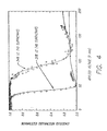
- FIG. 3 is a graph of both the threshold rms voltage 20 and the complete switching rms voltage 22 needed for switching a hologram made according to the teachings of this disclosure to minimum diffraction efficiency versus the frequency of the rms voltage.
- the threshold and complete switching rms voltages are reduced to 20 Vrms and 60 Vrms, respectively, at 10 kMz. Lower values are expected at even higher frequencies.
- FIG. 5 is a graph of the normalized net transmittance and normalized net diffraction efficiency of a hologram made according to the teachings of this disclosure versus temperature.
- polymer dispersed liquid crystal materials described herein successfully demonstrate the utility for recording volume holograms of a particular composition for such polymer dispersed liquid crystal systems.
- a PDLC reflection grating is prepared by placing several drops of the mixture of prepolymer material 112 on an indium-tin oxide coated glass slide 114 a .
- a second indium-tin oxide coated slide 114 b is then pressed against the first, thereby causing the prepolymer material 112 to fill the region between the slides 114 a and 114 b .
- the separation of the slides is maintained at approximately 20 ⁇ m by utilizing uniform spacers 118 .
- Preparation, mixing and transfer of the prepolymer material is preferably done in the dark.
- a mirror 116 may be placed directly behind the glass plate 114 b .
- the distance of the mirror from the sample is preferably substantially shorter than the coherence length of the laser.
- the PDLC material is preferably exposed to the 488 nm line of an argon-ion laser, expanded to fill the entire plane of the glass plate, with an intensity of approximately 0.1-100 mWatts/cm 2 with typical exposure times of 30-120 seconds. Constructive and destructive interference within the expanded beam establishes a periodic intensity profile through the thickness of the film.
- the prepolymer material utilized to make a reflection grating comprises a monomer, a liquid crystal, a cross-linking monomer, a co-initiator, and a photo-initiator dye.
- the reflection grating may be formed from prepolymer material comprising by total weight of the monomer dipentaerythritol hydroxypentacrylate (DPHA), 35% by total weight of a liquid crystal comprising a mixture of cyano biphenyls (known commercially as “E 7 ”), 10% by total weight of a cross-linking monomer comprising N-vinylpyrrolidinone (“NVP”), 2.5% by weight of the co-initiator N-phenylglycine (“NPG”), and 10 ⁇ 5 to 10 ⁇ 6 gram moles of a photo-initiator dye comprising rose bengal ester.
- DPHA monomer dipentaerythritol hydroxypentacrylate
- E 7 a mixture of cyan
- grating 130 includes periodic planes of polymer channels 130 a and PDLC channels 130 b which run parallel to the front surface 134 .
- the grating spacing associated with these periodic planes remains relatively constant throughout the full thickness of the sample from the air/film to the film/substrate interface.
- the morphology of the reflection grating differs significantly. In particular, it has been determined that, unlike transmission gratings with similar liquid crystal concentrations, very little coalescence of individual droplets was evident. Further more, the droplets that were present in the material were significantly smaller having diameters between 50 and 100 nm. Furthermore, unlike transmission gratings where the liquid crystal-rich regions typically comprise less than 40% of the grating, the liquid crystal-rich component of a reflection grating is significantly larger. Due to the much smaller periodicity associated with reflection gratings, i.e., a narrower grating spacing ( ⁇ 0.2 microns), it is believed that the time difference between completion of curing in high intensity versus low intensity regions is much smaller. It is also believed that the fast polymerization, as evidenced by small droplet diameters, traps a significant percentage of the liquid crystal in the matrix during gelation and precludes any substantial growth of large droplets or diffusion of small droplets into larger domains.
- the reflection notch In PDLC materials that are formed with the 488 nm line of an argon ion laser, the reflection notch typically has a reflection wavelength at approximately 472 nm for normal incidence and a relatively narrow bandwidth. The small difference between the writing wavelength and the reflection wavelength (approximately 5%) indicates that shrinkage of the film is not a significant problem. Moreover, it has been found that the performance of such gratings is stable over periods of many months.
- suitable PDLC materials could be prepared utilizing monomers such as triethyleneglycol diacrylate, trimethylolpropanetriacrylate, pentaerythritol triacrylate, pentaerythritol tetracrylate, pentaerythritol pentacrylate, and the like.
- monomers such as triethyleneglycol diacrylate, trimethylolpropanetriacrylate, pentaerythritol triacrylate, pentaerythritol tetracrylate, pentaerythritol pentacrylate, and the like.
- co-initiators such as triethylamine, triethanolamine, N,N-dimethyl-2,6-diisopropylaniline, and the like could be used instead of N-phenylglycine.
- FIG. 8 a there is shown an elevational view of a reflection grating 130 made in accordance with this disclosure having periodic planes of polymer channels 130 a and PDLC channels 130 b disposed parallel to the front surface 134 of the grating 130 .
- the symmetry axis 136 of the liquid crystal domains is formed in a direction perpendicular to the periodic channels 130 a and 130 b of the grating 130 and perpendicular to the front surface 134 of the grating 130 .
- the symmetry axis 136 is already in a low energy state in alignment with the field E and will reorient.
- reflection gratings formed in accordance with the procedure described above will not normally be switchable.
- a reflection grating tends to reflect a narrow wavelength band, such that the grating can be used as a reflection filter.
- the reflection grating is formed so that it will be switchable. More particularly, switchable reflection gratings can be made utilizing negative dielectric anisotropy LCs (or LCs with a low cross-over frequency), an applied magnetic field, an applied shear stress field, or slanted gratings.
- liquid crystals having a negative dielectric anisotropy will rotate in a direction perpendicular to an applied field.
- the symmetry axis 136 of the liquid crystal domains formed with a liquid crystal having a negative ⁇ will also be disposed in a direction perpendicular to the periodic channels 130 a and 130 b of the grating 130 and to the front surface 135 of the grating.
- an electric field E is applied across such gratings, as shown in FIG.
- the symmetry axis of the negative ⁇ liquid crystal will distort and reorient in a direction perpendicular to the field E, which is perpendicular to the film and the periodic planes of the grating.
- the reflection grating can be switched between a state where it is reflective and a state where it is transmissive.
- Liquid crystals can be found in nature (or synthesized) with either positive or negative ⁇ . Thus, it is possible to use a LC which has a positive ⁇ at low frequencies, but becomes negative at high frequencies.
- the frequency (of the applied voltage) at which ⁇ changes sign is called the crossover frequency.
- the cross-over frequency will vary with LC composition, and typical values range from 1-10 kHz. Thus, by operating at the proper frequency, the reflection grating may be switched.
- low crossover frequency materials can be prepared from a combination of positive and negative dielectric anisotropy liquid crystals.
- a suitable positive dielectric liquid crystal for use in such a combination contains four ring esters as shown below:
- a strongly negative dielectric liquid crystal suitable for use in such a combination is made up of pyridazines as shown below:
- liquid crystal materials are available from LaRoche & Co., Switzerland. By varying the proportion of the positive and negative liquid crystals in the combination, crossover frequencies form 1.4-2.3 kHz are obtained at room temperature.
- Another combination suitable for use in the present embodiment is a combination of the following: p-pentylphenyl-2-chloro-4-(p-pentylbenzoyloxy) benzoate and benzoate. These materials are available from Kodak Company.
- switchable reflection gratings can be formed using positive As liquid crystals.
- FIG. 10 a such gratings are formed by exposing the PDLC starting material to a magnetic field during the curing process.
- the magnetic field can be generated by the use of Helmholtz coils (as shown in FIG. 10 a ), the use of a permanent magnet, or other suitable means.
- the magnetic field M is oriented parallel to the front surface of the glass plates (not shown) that are used to form the grating 140 .
- the symmetry axis 146 of the liquid crystals will orient along the field while the mixture is fluid.
- the field may be removed and the alignment of the symmetry axis of the liquid crystals will remain unchanged. (See FIG. 10 b .)
- an electric field is applied, as shown in FIG. 10 c the positive ⁇ liquid crystal will reorient in the direction of the field, which is perpendicular to the front surface of grating and to the periodic channels of the grating.
- FIG. 11 a depicts a slanted transmission grating 148 and FIG. 11 b depicts a slanted reflection grating 150 .
- a holographic transmission grating is considered slanted if the direction of the grating vector G is not parallel to the grating surface.
- the grating is said to be slanted if the grating vector G is not perpendicular to the grating surface.
- Slanted gratings have many of the same uses as non-slanted grating such as visual displays, mirrors, line filters, optical switches, and the like.
- slanted holographic gratings are used to control the direction of a diffracted beam.
- a slanted grating is used to separate the specular reflection of the film from the diffracted beam.
- a slanted grating has an even more useful advantage.
- the slant allows the modulation depth of the grating to be controlled by an electric field when using either tangential or homeotropic aligned liquid crystals. This is because the slant provides components of the electric field in the directions both tangent and perpendicular to the grating vector.
- the LC domain symmetry axis will be oriented along the grating vector G and can be switched to a direction perpendicular to the film plane by a longitudinally applied field E.
- This is the typical geometry for switching of the diffraction efficiency of the slanted reflection grating.
- a conventional beam splitter splits the incident laser beam into two beams which are directed to the front faces of the prisms, and then overlapped in the sample at the desired angle. The beams thus enter the sample from opposite sides.
- This prism coupling technique permits the light to enter the sample at greater angles.
- the slant of the resulting grating is determined by the angle which the prism assembly is rotated (i.e., the angle between the direction of one incident beam and the normal to the prism front face at which that beam enters the prism).
- switchable reflection gratings may be formed in the presence of an applied shear stress field.
- a shear stress would be applied along the direction of a magnetic field M. This could be accomplished, for example, by applying equal and opposite tensions to the two ITO coated glass plates which sandwich the prepolymer mixture while the polymer is still soft. This shear stress would distort the LC domains in the direction of the stress, and the resultant LC domain symmetry axis will be preferentially along the direction of the stress, parallel to the PDLC planes and perpendicular to the direction of the applied electric field for switching.
- Reflection grating prepared in accordance with this description may find application in color reflective displays, switchable wavelength filters for laser protection, reflective optical elements and the like.
- PDLC materials can be made that exhibit a property known as form birefringence whereby polarized light that is transmitted through the grating will have its polarization modified.
- gratings are known as subwavelength gratings, and they behave like a negative uniaxial crystal, such as calcite, potassium dihydrogen phosphate, or lithium niobate, with an optic axis perpendicular to the PDLC planes.
- FIG. 13 there is shown an elevational view of a transmission grating 200 made in accordance with this description having periodic planes of polymer planes 200 a and PDLC planes 200 b disposed perpendicular to the front surface 204 of the grating 200 .
- the optic axis 206 is disposed perpendicular to polymer planes 200 a and the PDLC planes 200 b .
- Each polymer plane 200 a has a thickness t p and refractive index n p
- each PDLC plane 200 b has a thickness t PDLC and refractive index n PDLC .
- the grating will exhibit form birefringence.
- the magnitude of the shift in polarization is proportional to the length of the grating.
- /2, and to form a quarter-wave plate, the retardance must be equal to one-quarter of a wavelength, i.e., retardance
- is the difference between the ordinary index of refraction, n o , and the extraordinary index of refraction n e , of the sub-wavelength grating by the following relation:
- the length of the subwavelength grating should be selected so that:
- the length of the subwavelength grating should be selected so that:
- the polarization of the incident light is at an angle of 45° with respect to the optic axis 210 of a half-wave plate 212 , as shown in FIG. 14 a , the plane polarization will be preserved, but the polarization of the wave exiting the plate will be shifted by 90°.
- the half-wave plate 212 is placed between cross-polarizers 214 and 216 , the incident light will be transmitted. If an appropriate switching voltage is applied, as shown in FIG. 14 d , the polarization of the light is not rotated and the second polarizer will block the light.
- FIG. 16 a there is shown an elevational view of a subwavelength grating 230 recorded in accordance with the above-described methods and having periodic planes of polymer channels 230 a and PDLC channels 230 b disposed perpendicular to the front surface 234 of grating 230 .
- the symmetry axis 232 of the liquid crystal domains is disposed in a direction parallel to the front surface 234 of the grating and perpendicular to the periodic channels 230 a and 230 b of the grating 230 .
- the symmetry axis 232 distorts and reorients in a direction along the field E, which is perpendicular to the front surface 234 of the grating, and parallel to the periodic channels 230 a and 230 b of the grating 230 .
- subwavelength grating 230 can be switched between a state where it changes the polarization of the incident radiation and a state in which it does not.
- the direction of the liquid crystal domain symmetry 232 is due to a surface tension gradient which occurs as a result of the anisotropic diffusion of monomer and liquid crystal during recording of the grating, and that this gradient causes the liquid crystal domain symmetry to orient in a direction perpendicular to the periodic planes.
- n e 2 ⁇ n o 2 ⁇ [(f PDLC )(f p ) (n PDLC 2 ⁇ n p 2 )]/[f PDLC n PDLC 2 +f p n p 2 ]
- n o the ordinary index of refraction of the subwavelength grating
- n e the extraordinary index of refraction
- n PDLC the refractive index of the PDLC plane
- n p the refractive index of the polymer plane
- n LC the effective refractive index of the liquid crystal seen by an incident optical wave
- f PDLC t PDLC /(t PDLC + t P )
- f P t P /(t PDLC + t P )
- the effective refractive index of the liquid crystal, n LC is a function of the applied electric field, having a maximum when the field is zero and value equal to that of the polymer, n P , at some value of the electric field, E MAX .
- E MAX the electric field
- the refractive index of the liquid crystal, n LC , and, hence, the refractive index of the PDLC plane can be altered.
- ⁇ n ⁇ [(f PDLC )(f p )(n PDLC ⁇ n p 2 ) ]/[2n AVG (f PDLC n PDLC 2 +f p n p 2 )]
- n AVG (n e +n o )/2
- the refractive index of the PDLC plane n PDLC is related to the effective refractive index of the liquid crystal seen by an incident optical wave, n LC , and the refractive index of the surrounding polymer plane, n P , by the following relation:
- N PDLC n P +f LC [n LC ⁇ n P ]
- f LC is the volume fraction of liquid crystal dispersed in the polymer within the PDLC plane
- f LC [V LC /(V LC +V P )].
- n LC 1.7
- n P 1.5
- the net birefringence, ⁇ n, of the subwavelength grating is approximately 0.008.
- the length of the subwavelength grating should be 50 ⁇ m for a half-wave plate and a 25 ⁇ m for a quarter-wave plate.
- the refractive index of the liquid crystal can be matched to the refractive index of the polymer and the birefringence of the subwavelength grating turned off.
- the switching voltage, V n for a half-wave plate is on the order of 250 volts, and for a quarter-wave plate approximately 125 volts.
- the plates can be switched between the on and off (zero retardance) states on the order of microseconds.
- current Pockels cell technology can be switched in nanoseconds with voltages of approximately 1000-2000 volts, and bulk nematic liquid crystals can be switched on the order of milliseconds with voltages of approximately 5 volts.
- the switching voltage of the subwavelength grating can be reduced by stacking several subwavelength gratings 220 a - 220 e together, and connecting them electrically in parallel.
- a stack of five gratings each with a length of 10 ⁇ m yields the thickness required for a half-wave plate.
- the length of the sample is somewhat greater than 50 ⁇ m, because each grating includes an indium-tin-oxide coating which acts as a transparent electrode.
- the switching voltage for such a stack of plates is only 50 volts.
- Subwavelength gratings in accordance with the this description are expected to find suitable application in the areas of polarization optics and optical switches for displays and laser optics, as well as tunable filters for telecommunications, colorimetry, spectroscopy, laser protection, and the like.
- electrically switchable transmission gratings have many applications for which beams of light must be deflected or holographic images switched. Among these applications are: Fiber optic switches, reprogrammable N ⁇ N optical interconnects for optical computing, beam steering for laser surgery, beam steering for laser radar, holographic image storage and retrieval, digital zoom optics (switchable holographic lenses), graphic arts and entertainment, and the like.
- a switchable hologram is one for which the diffraction efficiency of the hologram may be modulated by the application of an electric field, and can be switched from a fully on state (high diffraction efficiency) to a fully off state (low or zero diffraction efficiency).
- a static hologram is one whose properties remain fixed independent of an applied field. In accordance with this description, a high contrast status hologram can also be created. In this variation of this description, the holograms are recorded as described previously. The cured polymer film is then soaked in a suitable solvent at room temperature for a short duration and finally dried. For the liquid crystal E 7 , methanol has shown satisfactory application.
- a high birefringence static sub-wavelength wave-plate can also be formed. Due to the fact that the refractive index for air is significantly lower than for most liquid crystals, the corresponding thickness of the half-wave plate would be reduced accordingly. Synthesized wave-plates in accordance with this description can be used in many applications employing polarization optics, particularly where a material of the appropriate birefringence that the appropriate wavelength is unavailable, too costly, or too bulky.
- polymer dispersed liquid crystals and polymer dispersed liquid crystal material includes, as may be appropriate, solutions in which none of the monomers have yet polymerized or cured, solutions in which some polymerization has occurred, and solutions which have undergone complete polymerization.
- polymer dispersed liquid crystals (which grammatically refers to liquid crystals dispersed in a fully polymerized matrix) is meant to include all or part of a more grammatically correct prepolymer dispersed liquid crystal material, or a more grammatically correct starting material for a polymer dispersed liquid crystal material.
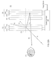
- FIG. 18 a shows a block diagram of an optical system 310 used in illuminating conventional image displays such as flat panel displays.
- Optical system 310 includes a first optical subsystem 312 , a quarter wave plate 314 , a second optical subsystem 316 , and a system controller 318 .
- First optical subsystem 312 includes three distinct holographic optical elements 312 a - 312 c .
- second optical subsystem 316 includes three holographic optical elements 316 a - 316 c .
- system controller 318 is individually coupled to each of the holographic optical elements 312 a - 312 c and 316 a - 316 c.
- each of the holographic optical elements 312 a - 312 c and 316 a - 316 c define a dynamic or switchable optical element configured to operate in active or inactive states depending upon a control signal provided by system controller 318 .
- each switchable holographic optical element In the active state, each switchable holographic optical element is designed to diffract a select bandwidth of visible light (e.g., red light) incident thereon.
- each switchable holographic optical element is configured to transmit substantially all light incident thereon without substantial alteration. In one sense, transmitting substantially all incident light without substantial alternation means that the optical element acts as a visibly transparent medium such as glass.
- the present invention can be employed with static holographic optical elements 312 a - 312 c and 316 a - 316 c that consistently diffract narrow bandwidth light, or with a combination of static and switchable holographic optical elements 312 a - 312 c and 316 a - 316 c .
- the present invention as shown in FIG. 18 a can be employed with a single switchable holographic optical element in each or either of the optical subsystems 312 and 316 .
- Such a single switchable holographic optical element operating in the active state in response to a single signal provided by system controller 318 , is configured to simultaneously diffract three distinct bandwidths of visible light (e.g., red, blue, and green, respectively).
- the optical subsystem employing a single switchable holographic optical element is configured to transmit substantially all light incident thereon without substantial alteration. Nonetheless, the present invention as shown in FIG. 18 a will be described with respect to optical subsystems 312 and 316 comprising individually switchable holographic optical elements, it being understood that the present invention as shown in FIG. 18 a is not limited thereto.
- FIG. 18 b shows a block diagram of a system 320 employing the present invention.
- System 320 includes first optical subsystem 322 , quarter wave plate 324 , second optical subsystem 326 , and system controller 328 .
- First optical subsystem 322 includes three holographic optical elements 322 a - 322 c .
- the second optical element subsystem 326 includes three holographic optical elements 326 a - 326 c .
- the second optical subsystem 326 defines a diffractive display for generating images in response to image signals received by system controller 328 as will be more fully described below.
- Each holographic optical element 322 a - 322 c comprises, in one embodiment, a switchable holographic optical element that operates between active and inactive states in response to control signals provided by system controller 328 .
- each switchable holographic optical element In the active state, each switchable holographic optical element is configured to diffract a select bandwidth of visible light (e.g., red light) incident thereon.
- each switchable holographic optical element 322 a - 322 c is configured to transmit substantially all visible light incident thereon without substantial alteration. It is noted, however, that each holographic optical element 322 a - 322 c may be defined as a static holographic optical element that consistently diffracts a select bandwidth of light incident thereon.
- first optical subsystem 322 may comprise a single switchable holographic optical element controlled by system controller 328 .
- This single switchable holographic optical element is switchable between active and inactive states in accordance with a control signal provided by system controller 328 . In the active state, this single switchable holographic optical element is configured to simultaneously diffract three distinct bandwidths of visible light incident thereon.
- the first optical subsystem 322 defined as a single switchable holographic optical element is configured to transmit substantially all visible light incident thereon without substantial alternation when operating in the inactive state.
- the system shown in FIG. 18 b will be described with reference to first optical subsystem 322 comprising three distinct switchable holographic optical elements each one switchable between active and inactive states. However, it is to be understood that the present invention is not to be limited thereto.
- the second optical subsystem 326 as shown in FIG. 18 b defines a diffractive display that includes three distinct switchable holographic optical elements 326 a - 326 c .
- each of the optical elements 326 a - 326 c includes a plurality of sub-areas. Each sub-area is individually switchable between the active state and the inactive state in accordance with control signals provided by system controller 328 . Each sub-area when activated, is configured to diffract a select bandwidth of visible light incident thereon. Moreover, each sub-area when inactive, is configured to transmit substantially all visible light incident thereon without substantial alteration.
- the subareas of each holographic optical element 326 a - 326 c are configured so that several may be active while the remainder are inactive in accordance with signals generated by system controller. Again, these features will be more fully described below.
- FIG. 19 a shows a cross sectional view of an example switchable holographic optical element that could be used within the first or second optical subsystems 312 and 316 shown in FIG. 18 a , or the first optical subsystem 322 shown in FIG. 18 b .
- the switchable holographic optical element 330 shown in FIG. 19 a includes a pair of substantially transparent and electrically nonconductive layers 332 , a pair of substantially transparent and electrically conductive layers 334 , and a switchable holographic layer 336 formed, in one embodiment, from the polymer dispersed liquid material described above.
- the substantially transparent, electrically nonconductive layers 332 comprise glass while the electrically conductive, substantially transparent layers 334 comprise indium tin oxide (ITO).
- ITO indium tin oxide
- An anti-reflection coating (not shown) may be applied to selected surfaces of the layered switchable holographic optical element including the ITO and the electrically nonconductive layers 332 , to improve the overall transmission efficiency of the optical element and to reduce stray light. As shown in this embodiment of FIG. 19 a , all layers 332 - 336 are arranged like a stack of pancakes on a common axis 338 .
- Layers 332 - 336 of the optical element 330 shown in FIG. 19 a may have substantially thin cross-sectional widths thereby providing a substantially thin aggregate in cross section. More particularly, switchable holographic layer 336 may have a cross-sectional width of 5-12 microns (the precise width depending on the spectral bandwidth and required diffraction efficiency) while glass layers 332 may have a cross-sectional width of 0.4-0.8 millimeters. Obviously, ITO layers 334 must be substantially thin to be transparent.
- ITO layers 334 are selectively coupled to a voltage source (not shown in FIG. 19 a or FIG. 19 b ) in accordance with a control signal provided by the system controller.
- a voltage source not shown in FIG. 19 a or FIG. 19 b
- an electric field is established within the switchable holographic layer 336 , and the switchable holographic optical element 330 is said to operate in the inactive state.
- an electric field established between ITO layers 334 deactivates the switchable holographic optical element layer 336 such that substantially all light incident upon either surface of transparent nonconductive layers 332 , regardless of incidence angle, is transmitted through the holographic optical element 330 without substantial alteration.
- the switchable holographic optical element 330 When the ITO layers 334 are disconnected from the voltage source, the switchable holographic optical element 330 is said to operate in the active state. More particularly, when ITO layers 334 are decoupled from a voltage source, no electric field is present therebetween and a select bandwidth of visible light is diffracted in holographic layer 336 . It is noted that switchable holographic layer 336 transmits light outside the select bandwidth without substantial alteration when activated.
- FIG. 19 b and 20 show an example of a switchable holographic optical element employed in the second optical subsystem (i.e., the diffractive display) of FIG. 18 b .
- FIG. 20 shows one embodiment of a system controller 328 shown in FIG. 18 b .
- FIG. 19 b shows a cross-sectional view of the switchable holographic optical element 340 shown in FIG. 20 taken along line 19 b.
- switchable holographic optical element 340 includes a pair of substantially transparent and electrically nonconductive layers 342 , a transparent and electrically conductive layer 344 , a switchable holographic layer 346 formed, in one embodiment, from the polymer dispersed liquid crystal material described above, and a layer 348 which comprises an array of substantially transparent and electrically conductive elements 350 electrically isolated by an electrically nonconductive isolator 352 .
- the substantially transparent, electrically nonconductive layers 342 comprise glass while the electrically conductive, substantially transparent layer 344 and elements 350 of layer 348 comprise indium tin oxide (ITO).
- ITO indium tin oxide
- Anti-reflection coatings may be provided on selected surfaces of the layers shown in FIG.
- all layers 342 - 348 are arranged like a stack of pancakes on a common axis 354 .
- Layers 342 - 348 may have substantially thin cross-sectional widths thereby provided a substantially thin switchable holographic optical element in the aggregate. More particularly, switchable holographic layer 346 may have a cross-sectional width of 5-12 microns (the precise width depending on the spectral bandwidth and required diffraction efficiency) while glass layers 342 may have a cross-sectional width of 0.4-0.8 millimeters. ITO elements 350 must have a substantially thin cross section to be transparent.
- each ITO element 350 is selectively coupled to a voltage source 356 contained within system controller 328 via thin conductive lines 360 , multiplexers 362 and switches 364 , wherein the multiplexers 362 and switchers 364 operate in accordance with control signals generated by control logic circuit 366 , which in turn operates in accordance with received image signals.
- the control signals generated by control logic circuit 366 are such that any one or more of the ITO elements 350 are coupled to voltage source 356 at any one point in time. Alternatively, all ITO elements may be decoupled from voltage source 356 at any point in time.
- FIG. 20 shows a 4 ⁇ 4 array of ITO elements 350 with a substantial distance between each filled by electrically nonconductive isolator. It is to be noted that the switchable holographic optical element 340 shown in FIG. 20 may have application with an array having a greater number of rows and columns of ITO elements 350 . Further FIG. 20 shows a large spacing between ITO layers so that conductive lines 360 can be easily identified. In practice, the spacing between ITO elements 350 need not be so large.
- ITO layer 344 is generally coupled to one terminal (i.e., ground) of voltage source 356 (not shown in FIG. 19 b ). Accordingly, when one of the ITO elements 350 is coupled to the positive terminal of voltage source 356 , a corresponding electric field is established within the underlying subarea of switchable holographic layer 356 . Those subareas of switchable holographic layer 346 where an electric field is established are said to operate in the inactive state. The subareas of switchable holographic layer 346 where no electric field is established are said to operate in the active state. Inactive subareas transmit substantially all light incident thereon without substantial alteration. In contrast, subareas that are activated diffract select bandwidth of light incident thereon.
- Switchable holographic layers 336 of FIG. 19 a and 346 of Fib. 19 b record holograms, in one embodiment, using the techniques described above.
- a high diffraction efficiency and a fast rate at which the optical element can be switched between active and inactive states characterize the resulting holograms.
- the recorded holograms can be switched from a diffracting state to a passing state with the creation and elimination of the electric field mentioned above.
- the holograms would be Bragg (also known as thick or volume phase) type in order to achieve high diffraction efficiency, or Raman Nath (also known as thin phase) type in order to achieve high angular bandwidth.
- the hologram recorded in switchable holographic layers 336 and 346 can be based on PDLC materials.
- the holograms result in an interference pattern created by recording beams, i.e., a reference beam and an object beam, within layer 336 or 346 .
- Interaction of the laser light with the PDLC material causes photo-polymerization.
- Intersection of the recording beams during the hologram recording process results in gratings (e.g., Bragg gratings) containing alternate liquid crystal droplets (i.e., high concentration of liquid crystal in polymer) and polymer (i.e., hardly any liquid crystal) surfaces.
- gratings e.g., Bragg gratings
- alternate liquid crystal droplets i.e., high concentration of liquid crystal in polymer
- polymer i.e., hardly any liquid crystal
- the liquid crystal droplets in layer 336 reorient and change the refractive index of the layer thereby essentially erasing the hologram recorded therein.
- the material used within layers 336 and 346 is configured to operate at a high switching rate (e.g., the material can be switched in tens of microseconds, which is very fast when compared with conventional liquid crystal display materials) and a high diffraction efficiency.
- FIGS. 21 a - 21 c illustrate operational aspects of one embodiment of the optical system 310 shown in FIG. 18 a .
- FIGS. 21 a-c show a conventional flat panel display 370 and a conventional beam splitter 372 .
- first optical subsystem 312 comprises three thin phase, transmissive type switchable holographic optical elements 312 a - 312 c .
- transmissive type relates to a switchable holographic optical element which emits diffracted light from a surface opposite the surface that receives light to be diffracted.
- transmissive type relates to a switchable holographic optical element which emits diffracted light from a surface opposite the surface that receives light to be diffracted.
- second optical subsystem 316 comprises three volume phase, reflective type switchable holographic optical elements 316 a - 316 c .
- a reflective type holographic optical element emits diffracted light from the same surface that receives light to be diffracted.
- the optical system 310 shown in FIGS. 21 a-c illustrates a technique that uses the angular sensitivity and polarization characteristics of the switchable holographic optical elements 312 a - 312 c and 316 a - 316 c to illuminate the flat panel 370 using only ambient light.
- Ambient light is incident on the first optical subsystem 312 over a range of incidence angles ranging from approximately 40 degrees to grazing.
- FIG. 21 a illustrates the propagation of one such ray RI incident on the front surface of first optical subsystem 312 .
- system controller 318 activates holographic optical elements 312 a and 316 a and deactivates holographic optical elements 312 b , 312 c , 316 b and 316 c .
- Activated holographic optical elements 312 a and 316 a operate to diffract a select bandwidth of visible light incident thereon.
- optical elements 312 a and 316 a when activated, operate to diffract a narrow bandwidth of red light. Light of bandwidths outside of narrow red bandwidth are transmitted through activated optical elements 312 a and 316 a without substantial alteration.
- Optical elements 312 b , 312 c , 316 b , and 316 c when inactive, operate to transmit substantially all light incident thereon without substantial alteration.
- a ambient ray R 1 constitutes the narrow red bandwidth component of ambient light.
- R 1 after being received at the front surface of activated optical element 312 a , is diffracted into a zero order beam R 4 and first order diffracted beams R 2 and R 3 .
- the transmissive type switchable holographic optical elements 312 a - 312 c are designed so that rays, such as RI, with predominantly large incidence angles measured with respect to the optical axis 374 which is normal to the front surface, are diffracted to produce first order rays, such as R 3 , which have directions making a small emergence angle measured with respect to the optical axis 374 .
- incidence angles of rays R 1 in the range of 40-90° will result in diffracted emergence angles covering an emergence angle range of approximately 20° in air.
- transmissive type electrically switchable holographic optical elements used in this embodiment tend to give maximum diffraction efficiency for p-polarized light, that is for light rays whose polarization vector lies in the plane of incidence.
- the diffraction efficiency for light polarized in a direction normal to the plane of incidence, that is the s-polarized light can be as low as a few percent of the maximum p-polarized diffraction efficiency.
- the reflective type switchable holographic optical elements used in this embodiment do not exhibit a preference for any particular polarization state, at least over the range of incident angles considered by the present invention.
- R 3 is p-polarized light.
- R 3 becomes circularly polarized and is received on the front surface of activated reflective type switchable holographic optical element 316 a .
- optical element 316 a diffracts R 3 , the diffracted light ( 5 ) emerging from the front surface of optical element 316 a .
- R 3 Since the variations in directions of R 3 tend to be small, R 3 will satisfy the Bragg diffraction equation for the volume phase reflective type holographic optical element 316 a .
- the diffracted ray will not suffer a polarization change since the reflective type hologram 316 a is not polarization sensitive. Accordingly, the ray diffracted by activated holographic optical element 316 a passes through quarter wave plate 314 and acquires a polarization orthogonal to that of R 3 . In other words, after passing through quarter wave plate 314 the ray will become predominantly s-polarized.
- This s-polarized ray is not significantly diffracted by any of the optical elements 312 a - 312 c it being understood that activated holographic optical element 312 a is not sensitive to s-polarized light. Thus, the s-polarized light transmits through activated optical element 312 a substantially unaltered.
- R 5 After emerging from the first optical subsystem, R 5 is reflected off beam splitter 372 and illuminates flat panel display 370 . Accordingly, it is seen that ambient light R 1 is collected from a variety of incidence angles to illuminate flat panel display 370 for a viewer 376 .
- FIG. 21 b shows operational aspects of the optical system 310 of FIG. 21 a after system controller 318 deactivates optical elements 312 a and 316 a , activates optical elements 312 b and 316 b while maintaining optical elements 312 c and 316 c in the inactive state.
- Optical elements 312 b and 316 b are designed to diffract narrow band blue light when activated. Further, when activated, optical elements 312 b and 316 b transmit substantially all light outside narrow band blue light without substantial alteration.
- the operational aspects shown in FIG. 21 b are substantially similar to that shown in FIG. 21 a with ray R 1 representing the blue bandwidth component of ambient light. Accordingly, ray R 1 is converted by optical system 310 into ray R 5 which is used to illuminate flat panel display 370 via beam splitter 372 .
- FIG. 21 c shows operational aspects of the optical system 310 of FIG. 21 b after system controller 318 activates optical elements 312 c and 316 c and deactivates optical elements 312 b and 316 b while maintaining optical elements 312 a and 316 a in the inactive status.
- Optical elements 312 c and 316 c are designed to diffract narrow band green light when active. Further, when active, optical elements 312 c and 316 c transmit substantially all light outside of narrow band green light without substantial alteration.
- the operational aspects shown in FIG. 21 c are substantially similar to that shown in FIGS. 21 a and 21 b with ray R 1 representing the green bandwidth component of ambient light. Accordingly, ambient light ray R 1 of narrow band green light is converted by optical system 310 into ray R 5 which is used to illuminate flat panel display 370 via beam splitter 372 .
- System controller 318 continuously cycles the activation and deactivation of pairs of optical elements within subsystems 312 and 316 as described in FIGS. 21 a - 21 c .
- flat panel display 370 is cyclically illuminated with red, blue, and green bandwidth light as corresponding monochrome components of full images are sequentially displayed. If the cycle time is sufficiently fast, viewer 376 will eye integrate the three red, blue, and green illuminated monochrome components to observe a sequence of full color images.
- optical elements 312 a - 312 c comprise thin phase holograms while optical elements 316 a - 316 c comprise volume phase holograms.
- Volume phase have higher diffraction efficiencies when compared to thin phase holograms.
- volume phase holograms have a theoretical maximum diffraction efficiency of 100%.
- the diffracted light will have two main components, a zero order beam, which propagates in the direction of the incident beam and first order diffracted beams that satisfy the Bragg diffraction relation, which will normally carry the bulk of the diffracted light energy.
- Angular bandwidth is determined by the Kogelnik coupled wave theory which states that high Bragg efficiencies will only occur for incident beams that are within a few degrees of the theoretical beam incidence angle that exactly satisfies the Bragg diffraction condition. Thin phase holograms, in contrast, will give rise to ⁇ 1 diffracted orders and a zero order.
- transmissive type switchable holographic optical elements 312 a - 312 c comprise thin phase holograms having a wide angular bandwidth. This high angular bandwidth in essence allows the optical system 310 to collect ambient light over a large range of incidence angles made with respect with the optical axis 374 .
- the reflective type holographic optical elements 316 a - 316 c comprise volume phase holograms with a smaller angular bandwidth but higher diffraction efficiency.
- R 3 has a relatively small angle of incidence when received by the second optical subsystem, substantially all diffractive light R 3 satisfies the Bragg edition. Accordingly, optical elements 316 a - 316 c provide a high diffraction efficiency with respect to incident rays R 3 .
- optical elements 312 a - 312 c in FIGS. 21 a - 21 c may comprise volume phase holograms.
- volume phase holograms with their narrower angular bandwidth may limit collection of ambient light to a narrower range of incidence angles.
- first optical subsystem 312 employing volume phase holograms may not provide as much of a concentrated beam for illumination of flat panel display 370 when compared to first optical subsystem comprising thin phase transmissive type holograms.
- ⁇ is the wavelength
- ⁇ is the grating period
- d is the thickness of the holographic medium
- n is the refractive index of the holographic medium
- thin phase holograms typically have Q values smaller than one while volume phase holograms have Q values greater than one.
- a more complete distinction between thin phase and volume phase holograms can be found within Klein, W. R. and Cook, B. D., IEEE Transactions on Sonics and Ultrasonics SU-14, pp. 123-134 (1967).
- FIGS. 22 a - 22 c illustrate operational aspects of one embodiment of the optical system 320 shown in FIG. 18 b .
- first optical subsystem 322 comprises three thin phase transmissive switchable holographic optical elements 322 a - 322 c that cyclically and sequentially diffracts red, green, and blue bandwidth light.
- each of the optical elements 322 a - 322 c is defined by the structure shown in FIG. 19 a .
- first optical subsystem may define a single switchable holographic optical element which simultaneously diffracts red, green, and blue bandwidth light in response to a single activation signal generated by system controller.
- the first optical subsystem may also comprise a single or three distinct static holographic optical elements that simultaneously and continuously diffract red, green, and blue bandwidth light. The present embodiment will be described with first optical subsystem comprising three switchable holographic optical elements.
- the second optical subsystem 326 defines a diffractive display and comprises three volume phase switchable reflective holographic optical elements 326 a - 326 c .
- Each of the optical elements 326 a - 326 c comprises, in one embodiment, the structure shown in FIGS. 19 b and 20 .
- system controller 328 can simultaneously activate one or more of the ITO elements 350 (See FIGS. 19 b and 20 ) of one or all three of the optical elements 326 a - 326 c in response to receiving one or three frames of image signals, respectively.
- the present embodiment will be described with respect to system controller activating one or more of the ITO elements 350 of a one of the optical elements 326 a - 326 c in response to receiving a single frame of image signals.
- system controller 328 activating corresponding pairs of optical elements in both the first and second optical subsystems at any one time while deactivating the remaining optical elements.
- optical elements 322 a and 326 a are activated while the remaining are deactivated
- optical elements 322 b and 326 b are activated while the remaining are deactivated
- optical elements 322 c and 326 c are activated while the remaining are deactivated.
- optical element 322 a in FIGS. 22 a - 22 c diffracts the p-polarized red bandwidth component of light incident thereon when operating in the active state. Further, optical element 322 a passes the remaining components of the incident light without substantial alteration when operating in the active state. In the inactive state, optical element 322 a passes substantially all incident light without substantial alteration.
- Optical element 322 b when operating in the active state, diffracts the p-polarized blue bandwidth component of incident light while passing the remaining components without substantial alteration. In the inactive state, optical element 322 b passes substantially all incident light without substantial alteration.
- Optical element 322 c when activated, diffracts the p-polarized green bandwidth component of incident light while passing the remaining components without substantial alteration.
- Optical element 322 c in the inactive state, passes substantially all components of incident light without substantial alteration.
- Activated subareas of optical element 326 a diffract red bandwidth light circularly polarized by quarter wave plate 324 while passing the remaining components of the incident light without substantial alteration.
- the red bandwidth light diffracted by activated subareas in optical element 326 a emerges from the same surface that receives the incident light.
- Inactive subareas of optical element 326 a pass substantially all light incident thereon without substantial alteration.
- Activated subareas of optical element 326 b diffract blue bandwidth light circularly polarized by quarter wave plate 324 while passing the remaining components thereof without substantial alteration.
- the blue bandwidth light diffracted by optical element 326 b emerges from the same surface that receives the incident light.
- the inactive subareas of optical element 326 b pass substantially all incident light without substantial alteration.
- the activated subareas of optical element 326 c diffracts green bandwidth light circularly polarized by quarter wave plate 324 while passing the remaining components thereof without substantial alteration.
- the diffracted green bandwidth light emerges from the same surface that receives the incident light.
- Deactivated subareas of optical element 326 c pass substantially all incident light without substantial alteration.
- the operational aspects of system 320 shown in FIGS. 22 a - 22 c are in many ways similar to that shown in FIGS. 21 a - 21 c . More particularly, the first optical subsystem 322 collects ambient light over a range of incidence angles. In FIG. 22 a , system controller 328 activates optical element 322 a . Additionally, system controller 328 activates one or more subareas of optical element 326 a in response to receiving a frame of image signals. The remaining optical components are rendered inactive by system controller 328 . In FIG. 22 a , ambient ray R 1 comprises the p-polarized red bandwidth component of ambient light.
- R 1 after being received by activated optical element 322 a , is diffracted into a zero order beam R 4 and first order diffracted beams R 2 and R 3 .
- the thin phase transmissive type switchable holographic optical elements 322 a - 322 c are designed so that rays, such as R 1 , with predominantly large incidence angles, are diffracted to give rise to diffractive first order rays, such as R 3 , that have directions making a small emergence angle with respect to the optical axis 374 .
- Diffracted p-polarized red bandwidth light R 3 passes through quarter wave plate 324 and becomes circularly polarized before it is received by an activated or deactivated subarea of optical element 326 a .
- R 3 being received by an activated subarea of optical element 326 a .
- the activated subarea of optical element 326 a diffracts R 3 , the diffracted light R 5 emerging from the same surface that receives R 3 .
- R 5 passes back through quarter wave plate 324 and acquires a polarization state orthogonal to that of R 3 . In other words, after passing through quarter wave plate 324 , R 5 will become predominantly s-polarized.
- R 5 passes through optical elements 322 a - 322 c without substantial alteration to be viewed by observer 376 .
- FIG. 22 b shows system 320 of FIG. 22 a just after system controller deactivates optical elements 322 a and 326 a and activates optical element 322 b and one or more subareas of optical element 326 b .
- the subareas of optical element 326 b are activated by controller 328 in response to controller 328 receiving a frame of image signals.
- ambient ray R 1 comprises the p-polarized blue bandwidth component of ambient light.
- R 1 passes through optical element 322 a without substantial alteration.
- R 1 after being received by activated optical element 322 b , is diffracted into a zero order beam R 4 and first order diffracted beams R 2 and R 3 .
- Diffracted p-polarized blue bandwidth light R 3 passes through quarter wave plate 324 and becomes circularly polarized before it is received by an activated or deactivated subarea of optical element 326 b .
- the present embodiment will be described with reference to R 3 being received by an activated subarea of optical element 326 b .
- the activated subarea of optical element 326 b diffracts R 3 , the diffracted light R 5 emerging from the same surface that receives R 3 .
- R 5 passes back through quarter wave plate 324 and acquires a polarization state orthogonal to that of R 3 . In other words, after passing through quarter wave plate 324 , R 5 will become predominantly s-polarized.
- R 5 passes through optical elements 322 a - 322 c without substantial alteration to be viewed by observer 376 .
- FIG. 22 c shows system 320 of FIG. 22 b just after system controller deactivates optical elements 322 b and 326 b and activates optical element 322 c and one or more subareas of optical element 326 c .
- the subareas of optical element 326 c are activated by controller 328 in response to controller 328 receiving a frame of image signals.
- ambient ray R 1 comprises the p-polarized green bandwidth component of ambient light.
- R 1 passes through optical element 322 a and 322 b without substantial alteration.
- R 1 after being received by activated optical element 322 c , is diffracted into a zero order beam R 4 and first order diffracted beams R 2 and R 3 .
- Diffracted p-polarized green bandwidth light R 3 passes through quarter wave plate 324 and becomes circularly polarized before it is received by an activated or deactivated subarea of optical element 326 c .
- the present embodiment will be described with reference to R 3 being received by an activated subarea of optical element 326 c .
- the activated subarea of optical element 326 b diffracts R 3 , the diffracted light R 5 emerging from the same surface that receives R 3 .
- R 5 passes back through quarter wave plate 324 and acquires a polarization state orthogonal to that of R 3 . In other words, after passing through quarter wave plate 324 , R 5 will become predominantly s-polarized.
- R 5 passes through optical elements 322 a - 322 c without substantial alteration to be viewed by observer 376 .
Abstract
Description


| no = | the ordinary index of refraction of the subwavelength grating; |
| ne = | the extraordinary index of refraction; |
| nPDLC = | the refractive index of the PDLC plane; |
| np = | the refractive index of the polymer plane |
| nLC = | the effective refractive index of the liquid crystal seen by an |
| incident optical wave; | |
| fPDLC = | tPDLC/(tPDLC + tP) |
| fP = | tP/(tPDLC + tP) |
Claims (66)
Priority Applications (1)
| Application Number | Priority Date | Filing Date | Title |
|---|---|---|---|
| US09/419,273 US6339486B1 (en) | 1998-10-16 | 1999-10-15 | Holographic technique for illumination of image displays using ambient illumination |
Applications Claiming Priority (2)
| Application Number | Priority Date | Filing Date | Title |
|---|---|---|---|
| US10447398P | 1998-10-16 | 1998-10-16 | |
| US09/419,273 US6339486B1 (en) | 1998-10-16 | 1999-10-15 | Holographic technique for illumination of image displays using ambient illumination |
Publications (1)
| Publication Number | Publication Date |
|---|---|
| US6339486B1 true US6339486B1 (en) | 2002-01-15 |
Family
ID=22300685
Family Applications (1)
| Application Number | Title | Priority Date | Filing Date |
|---|---|---|---|
| US09/419,273 Expired - Fee Related US6339486B1 (en) | 1998-10-16 | 1999-10-15 | Holographic technique for illumination of image displays using ambient illumination |
Country Status (3)
| Country | Link |
|---|---|
| US (1) | US6339486B1 (en) |
| AU (1) | AU1209100A (en) |
| WO (1) | WO2000023835A1 (en) |
Cited By (14)
| Publication number | Priority date | Publication date | Assignee | Title |
|---|---|---|---|---|
| US20050237589A1 (en) * | 2003-09-23 | 2005-10-27 | Sbg Labs, Inc. | Optical filter employing holographic optical elements and image generating system incorporating the optical filter |
| US20050277467A1 (en) * | 2004-06-14 | 2005-12-15 | Jcm American Corporation, A Nevada Corporation | Gaming machine using holographic imaging |
| US7176992B1 (en) * | 1999-08-12 | 2007-02-13 | Avago Technologies General Ip (Singapore) Pte. Ltd. | Methods of fabricating PDLC optical devices |
| US20070177239A1 (en) * | 2006-01-30 | 2007-08-02 | Konica Minolta Holdings, Inc. | Image display apparatus and head-mounted display |
| US20080151339A1 (en) * | 2006-12-21 | 2008-06-26 | Shigeru Oouchida | Light source unit and optical detection unit |
| US7616851B1 (en) * | 2008-06-26 | 2009-11-10 | Lockheed Martin Corporation | Tunable wavelength filter device |
| US20110285956A1 (en) * | 2009-02-03 | 2011-11-24 | Toppan Printing Co., Ltd. | Phase-type diffraction device, manufacturing method thereof and image pick-up apparatus |
| US20200011514A1 (en) * | 2018-02-27 | 2020-01-09 | Guangzhou Tyrafos Semiconductor Technologies Co., Ltd | Light-emitting apparatus |
| US11448937B2 (en) | 2012-11-16 | 2022-09-20 | Digilens Inc. | Transparent waveguide display for tiling a display having plural optical powers using overlapping and offset FOV tiles |
| US11543594B2 (en) | 2019-02-15 | 2023-01-03 | Digilens Inc. | Methods and apparatuses for providing a holographic waveguide display using integrated gratings |
| US11561409B2 (en) * | 2007-07-26 | 2023-01-24 | Digilens Inc. | Laser illumination device |
| US11592614B2 (en) | 2019-08-29 | 2023-02-28 | Digilens Inc. | Evacuated gratings and methods of manufacturing |
| US11740472B2 (en) | 2015-01-12 | 2023-08-29 | Digilens Inc. | Environmentally isolated waveguide display |
| US11754842B2 (en) | 2015-10-05 | 2023-09-12 | Digilens Inc. | Apparatus for providing waveguide displays with two-dimensional pupil expansion |
Families Citing this family (1)
| Publication number | Priority date | Publication date | Assignee | Title |
|---|---|---|---|---|
| CN101084638A (en) * | 2004-12-21 | 2007-12-05 | 皇家飞利浦电子股份有限公司 | Display device for visually reconstructing an image |
Citations (156)
| Publication number | Priority date | Publication date | Assignee | Title |
|---|---|---|---|---|
| US3807829A (en) | 1973-04-30 | 1974-04-30 | Hughes Aircraft Co | Extended-field holographic lens arrays |
| US4028725A (en) | 1976-04-21 | 1977-06-07 | Grumman Aerospace Corporation | High-resolution vision system |
| US4458981A (en) | 1982-01-26 | 1984-07-10 | Thomson-Csf | Holographic movie device |
| US4500163A (en) | 1981-07-29 | 1985-02-19 | The Singer Company | Holographic projection screen |
| DE3419098A1 (en) | 1984-05-23 | 1985-11-28 | Hartmut Dr. 8520 Erlangen Bartelt | Screen for spatial three-dimensional representation of images, graphics and other data |
| US4566031A (en) | 1984-02-16 | 1986-01-21 | The Holotronics Corporation | Spatial light modulation with application to electronically generated holography |
| US4669812A (en) | 1983-09-12 | 1987-06-02 | Hoebing John L | Method and apparatus for 3-D image synthesis |
| US4759596A (en) | 1984-08-30 | 1988-07-26 | Polaroid Corporation | Wavelength selective optical cavity including holographic filter layers |
| FR2610733A1 (en) | 1987-02-06 | 1988-08-12 | Ikeda Shigeru | IMAGE COMPOSER |
| US4790613A (en) | 1987-01-06 | 1988-12-13 | Hughes Aircraft Company | Holographic display panel for a vehicle windshield |
| US4799739A (en) | 1987-08-10 | 1989-01-24 | Advanced Dimensional Displays, Inc. | Real time autostereoscopic displays using holographic diffusers |
| US4807951A (en) | 1987-01-06 | 1989-02-28 | Hughes Aircraft Company | Holographic thin panel display system |
| US4830441A (en) | 1987-03-25 | 1989-05-16 | Kaiser Optical Systems | Holographic filter construction for protective eyewear |
| US4834473A (en) | 1986-03-26 | 1989-05-30 | The Babcock & Wilcox Company | Holographic operator display for control systems |
| US4834476A (en) | 1987-03-31 | 1989-05-30 | Massachusetts Institute Of Technology | Real image holographic stereograms |
| USH738H (en) | 1989-07-17 | 1990-02-06 | The United States Of America As Represented By The Secretary Of The Army | Switched holograms for reconfigurable optical interconnect |
| US4932731A (en) | 1986-11-14 | 1990-06-12 | Yazaki Corporation | Holographic head-up display apparatus |
| US4938568A (en) | 1988-01-05 | 1990-07-03 | Hughes Aircraft Company | Polymer dispersed liquid crystal film devices, and method of forming the same |
| EP0389123A2 (en) | 1989-03-21 | 1990-09-26 | Hughes Aircraft Company | A display system for multiviewer training simulators |
| US4981332A (en) | 1989-06-29 | 1991-01-01 | Hughes Aircraft Company | Dispersion-compensated windshield hologram virtual image display |
| US4993790A (en) | 1990-03-26 | 1991-02-19 | Rockwell International Corporation | Holographic lenticular screen stereoscopic avoinics display apparatus |
| US5011244A (en) | 1988-12-16 | 1991-04-30 | Hughes Aircraft Company | Holographic full color data retrieval and projection system |
| US5013141A (en) | 1985-02-21 | 1991-05-07 | Canon Kabushiki Kaisha | Liquid crystal light modulation device |
| US5014709A (en) | 1989-06-13 | 1991-05-14 | Biologic Systems Corp. | Method and apparatus for high resolution holographic imaging of biological tissue |
| US5024494A (en) | 1987-10-07 | 1991-06-18 | Texas Instruments Incorporated | Focussed light source pointer for three dimensional display |
| US5035474A (en) | 1984-04-16 | 1991-07-30 | Hughes Aircraft Company | Biocular holographic helmet mounted display |
| US5036385A (en) | 1986-03-07 | 1991-07-30 | Dimension Technologies, Inc. | Autostereoscopic display with multiple sets of blinking illuminating lines and light valve |
| US5044709A (en) | 1988-11-30 | 1991-09-03 | Hughes Aircraft Company | LED array polarized image source/0 degree hologram virtual image head up display |
| US5071209A (en) | 1990-05-07 | 1991-12-10 | Hughes Aircraft Company | Variable acuity non-linear projection system |
| US5093567A (en) | 1989-07-14 | 1992-03-03 | Gec-Marconi Limited | Helmet systems with eyepiece and eye position sensing means |
| US5093563A (en) | 1987-02-05 | 1992-03-03 | Hughes Aircraft Company | Electronically phased detector arrays for optical imaging |
| US5096282A (en) | 1988-01-05 | 1992-03-17 | Hughes Aircraft Co. | Polymer dispersed liquid crystal film devices |
| US5103323A (en) | 1990-04-18 | 1992-04-07 | Holographic Optics, Inc. | Multi-layer holographic notch filter |
| US5111313A (en) | 1989-08-10 | 1992-05-05 | Shires Mark R | Real-time electronically modulated cylindrical holographic autostereoscope |
| US5151724A (en) | 1991-01-30 | 1992-09-29 | Dan Kikinis | Dynamic holographic display with cantilever |
| US5153670A (en) | 1990-01-12 | 1992-10-06 | Physical Optics Corporation | Holographic lippmann-bragg filter in a spectroscopic system |
| US5175637A (en) | 1990-04-05 | 1992-12-29 | Raychem Corporation | Displays having improved contrast |
| GB2259213A (en) | 1991-08-29 | 1993-03-03 | British Aerospace | Variable resolution view-tracking display |
| US5221957A (en) | 1990-01-12 | 1993-06-22 | Physical Optics Corporation | Nonuniform holographic filter in a spectroscopic system |
| US5227898A (en) | 1991-12-02 | 1993-07-13 | Computer Sciences Corporation | Near real-time holographic display for remote operations |
| US5234449A (en) | 1992-07-16 | 1993-08-10 | Ethicon, Inc. | Suture clip with reduced hinge mass |
| EP0559435A1 (en) | 1992-03-05 | 1993-09-08 | International Business Machines Corporation | Improvements in holographic techniques |
| US5278532A (en) | 1987-09-14 | 1994-01-11 | Hughes Aircraft Company | Automotive instrument virtual image display |
| US5291314A (en) | 1990-07-27 | 1994-03-01 | France Telecom | Spatial light modulator device and a conoscopic holography system of large dynamic range including such a modulator device |
| US5299035A (en) | 1992-03-25 | 1994-03-29 | University Of Michigan | Holographic imaging through scattering media |
| US5305124A (en) | 1992-04-07 | 1994-04-19 | Hughes Aircraft Company | Virtual image display system |
| US5319492A (en) | 1991-05-23 | 1994-06-07 | Alcatel N.V. | Optical switch |
| EP0602813A1 (en) | 1992-12-17 | 1994-06-22 | International Business Machines Corporation | Hologram system and method |
| US5331149A (en) | 1990-12-31 | 1994-07-19 | Kopin Corporation | Eye tracking system having an array of photodetectors aligned respectively with an array of pixels |
| US5341229A (en) | 1988-07-14 | 1994-08-23 | Larry Rowan | Holographic display system |
| US5365354A (en) | 1990-10-02 | 1994-11-15 | Physical Optics Corporation | Grin type diffuser based on volume holographic material |
| US5379133A (en) | 1992-06-19 | 1995-01-03 | Atl Corporation | Synthetic aperture based real time holographic imaging |
| US5381253A (en) | 1991-11-14 | 1995-01-10 | Board Of Regents Of University Of Colorado | Chiral smectic liquid crystal optical modulators having variable retardation |
| US5414544A (en) | 1992-12-25 | 1995-05-09 | Sony Corporation | Display apparatus |
| US5418631A (en) | 1993-05-14 | 1995-05-23 | Kaiser Optical Systems, Inc. | Edge-lit holographic diffusers for flat-panel displays |
| US5424866A (en) | 1991-01-30 | 1995-06-13 | Kikinis; Dan | Dynamic holographic display with cantilever |
| EP0664495A1 (en) | 1994-01-21 | 1995-07-26 | Sharp Kabushiki Kaisha | Switchable holographic apparatus |
| US5440428A (en) | 1993-09-30 | 1995-08-08 | Hughes Aircraft Company | Automotive instrument 3-D virtual image display |
| US5455693A (en) | 1992-09-24 | 1995-10-03 | Hughes Aircraft Company | Display hologram |
| US5471327A (en) | 1993-05-14 | 1995-11-28 | Kaiser Optical Systems, Inc. | Holographic diffuser for back-lit display |
| US5497254A (en) | 1990-04-05 | 1996-03-05 | Seiko Epson Corporation | Optical apparatus including a liquid crystal modulator |
| US5506701A (en) | 1993-01-28 | 1996-04-09 | Dai Nippon Printing Co., Ltd. | Hologram color filter, liquid crystal display device using the same, and fabrication process of hologram color filter |
| US5521724A (en) | 1993-11-15 | 1996-05-28 | Shires; Mark R. | Real-time automultiscopic 3D video display using holographic optical elements (HOEs) |
| US5530565A (en) | 1992-11-30 | 1996-06-25 | Kaiser Optical Systems, Inc. | Holographic transmission bandpass filter |
| EP0720040A2 (en) | 1994-12-29 | 1996-07-03 | Sharp Kabushiki Kaisha | Illumination system and display device |
| US5535024A (en) | 1992-05-06 | 1996-07-09 | The United States Of America As Represented By The Secretary Of The Air Force | Photorefractive holographic interference novelty filter |
| US5537232A (en) | 1993-10-05 | 1996-07-16 | In Focus Systems, Inc. | Reflection hologram multiple-color filter array formed by sequential exposure to a light source |
| US5539542A (en) | 1991-06-19 | 1996-07-23 | France Telecom | Photorefractive device having an electro-optical material between two photoconductive materials |
| US5539544A (en) | 1992-02-18 | 1996-07-23 | Sextant Avionique | Holographic filter for protection from radiation, notably laser radiation |
| US5544143A (en) | 1994-06-14 | 1996-08-06 | Eastman Kodak Company | Read/write laser-detector-grating unit (LDGU) with an orthogonally-arranged focus and tracking sensor system |
| US5552912A (en) | 1991-11-14 | 1996-09-03 | Board Of Regents Of The University Of Colorado | Chiral smectic liquid crystal optical modulators |
| US5552916A (en) | 1990-09-07 | 1996-09-03 | Displaytech, Inc. | Diffractive light modulator |
| US5557283A (en) | 1991-08-30 | 1996-09-17 | Sheen; David M. | Real-time wideband holographic surveillance system |
| US5561537A (en) | 1992-09-30 | 1996-10-01 | Fujitsu Limited | Stereoscopic display method and apparatus |
| US5568313A (en) | 1992-08-18 | 1996-10-22 | Applied Physics Research, L.P. | Apparatus for providing autostereoscopic and dynamic images and method of manufacturing same |
| US5570208A (en) | 1992-08-21 | 1996-10-29 | Fujitsu Limited | Stereoscopic display method of hologram and its forming method and stereoscopic display apparatus |
| US5570139A (en) | 1994-05-13 | 1996-10-29 | Wang; Yu | Surface plasmon high efficiency HDTV projector |
| US5579026A (en) | 1993-05-14 | 1996-11-26 | Olympus Optical Co., Ltd. | Image display apparatus of head mounted type |
| US5581378A (en) | 1993-02-01 | 1996-12-03 | University Of Alabama At Huntsville | Electro-optical holographic display |
| US5589956A (en) | 1992-07-31 | 1996-12-31 | Canon Kabushiki Kaisha | Image display apparatus |
| US5589957A (en) | 1994-03-15 | 1996-12-31 | Fujitsu Limited | Stereoscopic display apparatus using cylindrical screen |
| US5594560A (en) | 1994-03-07 | 1997-01-14 | Motorola, Inc. | Display device comprising fluorescent enhanced reflective holographic illumination |
| US5606455A (en) | 1993-05-06 | 1997-02-25 | Dimension Technologies, Inc. | Autostereoscopic display with high power efficiency |
| US5608552A (en) | 1995-12-26 | 1997-03-04 | Hughes Electronics | Liquid crystal display having an off-axis full-color holographic filter |
| US5615186A (en) | 1991-06-04 | 1997-03-25 | International Business Machines Corporation | Multiple data surface data storage system with holographic filter element |
| US5615023A (en) | 1993-12-24 | 1997-03-25 | Hyundai Electronics Industrial Co., Ltd. | Head-up display for automobile |
| US5617225A (en) | 1992-07-20 | 1997-04-01 | Fujitsu Limited | Stereoscopic display apparatus and method |
| US5621547A (en) | 1990-11-23 | 1997-04-15 | Thomson-Csf | Illumination device and application to a display device |
| US5629784A (en) | 1994-04-12 | 1997-05-13 | Ois Optical Imaging Systems, Inc. | Liquid crystal display with holographic diffuser and prism sheet on viewer side |
| US5635947A (en) | 1993-08-16 | 1997-06-03 | Agency Of Industrial Science & Technology, Ministry Of International Trade & Industry | Eye movement tracking display |
| EP0777136A1 (en) | 1995-11-08 | 1997-06-04 | Victor Company Of Japan, Limited | Color filter and color image display apparatus employing the filter |
| US5640256A (en) | 1996-01-25 | 1997-06-17 | Board Of Trustees Of The Leland Stanfor Junior University | Dynamic multiple wavelength filter using a stratified volume holographic optical element |
| US5644369A (en) | 1995-02-24 | 1997-07-01 | Motorola | Switchable lens/diffuser |
| US5650865A (en) | 1995-03-21 | 1997-07-22 | Hughes Electronics | Holographic backlight for flat panel displays |
| EP0785457A2 (en) | 1996-01-17 | 1997-07-23 | Nippon Telegraph And Telephone Corporation | Optical device and three-dimensional display device |
| US5668648A (en) | 1991-11-26 | 1997-09-16 | Kabushiki Kaisha Toshiba | Computer-assisted holographic display apparatus |
| US5680231A (en) | 1995-06-06 | 1997-10-21 | Hughes Aircraft Company | Holographic lenses with wide angular and spectral bandwidths for use in a color display device |
| US5684498A (en) | 1995-06-26 | 1997-11-04 | Cae Electronics Ltd. | Field sequential color head mounted display with suppressed color break-up |
| US5692077A (en) | 1996-04-30 | 1997-11-25 | Wavefront Research, Inc. | Optical time shifter and routing system |
| US5696552A (en) | 1992-09-30 | 1997-12-09 | Fujitsu Limited | Stereoscopic display apparatus |
| US5696749A (en) | 1996-06-28 | 1997-12-09 | Eastman Kodak Company | Dual-wavelength optical recording head utilizing grating beam splitter and integrated laser and detectors |
| US5698343A (en) | 1994-07-05 | 1997-12-16 | The United States Of America As Represented By The Secretary Of The Air Force | Laser wavelength detection and energy dosimetry badge |
| US5703702A (en) | 1993-09-08 | 1997-12-30 | Crane; Patrick E. | Holographic synthesis |
| US5706067A (en) | 1995-04-28 | 1998-01-06 | International Business Machines Corporation | Reflective spatial light modulator array |
| US5708488A (en) | 1992-10-07 | 1998-01-13 | Matsushita Electric Industrial Co., Ltd. | Phase type spatial light modulator having an output substantially uniform in amplitude |
| US5709463A (en) | 1996-08-13 | 1998-01-20 | Delco Electronics Corporation | Backlighting for bright liquid crystal display |
| EP0821293A2 (en) | 1996-07-22 | 1998-01-28 | Dai Nippon Printing Co., Ltd. | Reflection type diffuse hologram, hologram for reflection hologram color filters, etc., and reflection type display device using such holograms |
| US5719690A (en) | 1996-05-31 | 1998-02-17 | International Business Machines Corporation | Photorefractive glass article |
| US5721598A (en) | 1995-12-26 | 1998-02-24 | Hughes Electronics | High efficiency, high color purity, on-axis holographic color filter and full-color liquid crystal display |
| US5721630A (en) | 1996-03-12 | 1998-02-24 | Polaroid Corporation | High-efficiency reflective holographic diffuser and method for making thereof |
| EP0825462A1 (en) | 1996-08-21 | 1998-02-25 | Sony Corporation | Holographic optical element process for its production and projection liquid crystal display apparatus using the element |
| EP0826986A1 (en) | 1996-08-21 | 1998-03-04 | Victor Company Of Japan, Limited | Color filter and color display apparatus |
| US5729366A (en) | 1993-12-23 | 1998-03-17 | Hyundas Electronics Industries Co., Ltd. | Heads-up display for vehicle using holographic optical elements |
| US5736958A (en) | 1990-10-29 | 1998-04-07 | Essex Corporation | Image synthesis using time sequential holography |
| US5739930A (en) | 1992-10-13 | 1998-04-14 | Fujitsu Limited | Display apparatus |
| US5745203A (en) | 1996-03-28 | 1998-04-28 | Motorola, Inc. | Liquid crystal display device including multiple ambient light illumination modes with switchable holographic optical element |
| US5744267A (en) | 1994-10-12 | 1998-04-28 | Arizona Board Of Regents Acting For And On Behalf Of University Of Arizona | Azo-dye-doped photorefractive polymer composites for holographic testing and image processing |
| US5748828A (en) | 1993-11-10 | 1998-05-05 | Alliedsignal Inc. | Color separating backlight |
| US5748272A (en) | 1993-02-22 | 1998-05-05 | Nippon Telegraph And Telephone Corporation | Method for making an optical device using a laser beam interference pattern |
| US5751243A (en) | 1990-10-29 | 1998-05-12 | Essex Corporation | Image synthesis using time sequential holography |
| US5760933A (en) | 1992-07-20 | 1998-06-02 | Fujitsu Limited | Stereoscopic display apparatus and method |
| US5764317A (en) | 1995-06-26 | 1998-06-09 | Physical Optics Corporation | 3-D volume visualization display |
| US5768242A (en) | 1996-04-05 | 1998-06-16 | The United States Of America As Representd By The Administrator Of The National Aeronautics And Space Administration | Apparatus and method for focusing a light beam in a three-dimensional recording medium by a dynamic holographic device |
| US5771320A (en) | 1996-04-30 | 1998-06-23 | Wavefront Research, Inc. | Optical switching and routing system |
| US5774175A (en) | 1992-10-14 | 1998-06-30 | Terumo Kabushiki Kaisha | Stereoscopic television |
| US5777760A (en) | 1996-05-10 | 1998-07-07 | Quantum Corporation | Position feedback system for volume holographic storage media |
| US5777742A (en) | 1993-03-11 | 1998-07-07 | Environmental Research Institute Of Michigan | System and method for holographic imaging with discernible image of an object |
| US5790284A (en) | 1993-06-01 | 1998-08-04 | Canon Kabushiki Kaisha | Display apparatus and displaying method for image display producing stereoscopic effect |
| EP0856766A2 (en) | 1997-01-31 | 1998-08-05 | Xerox Corporation | Holographically formed reflective display, liquid crystal display and projection system and methods of forming the same |
| EP0856768A2 (en) | 1997-01-31 | 1998-08-05 | Xerox Corporation | Broadband reflective display, and methods of forming the same |
| US5793504A (en) | 1996-08-07 | 1998-08-11 | Northrop Grumman Corporation | Hybrid angular/spatial holographic multiplexer |
| US5793503A (en) | 1992-01-03 | 1998-08-11 | Simian Company, Inc. | Methods of hologram construction using computer-processed objects |
| US5796499A (en) | 1997-02-28 | 1998-08-18 | Polaroid Corporation | Transmission holographic diffuser made and used to effect lateral color constancy in rear screen projection display systems |
| US5796498A (en) | 1992-02-14 | 1998-08-18 | Imperial College Of Science, Technology And Medicine | Holographic imaging |
| US5801799A (en) | 1996-12-23 | 1998-09-01 | Motorola, Inc. | Multi-directional liquid crystal phase spatial light modulator for enchanced display resolution |
| US5801798A (en) | 1996-12-23 | 1998-09-01 | Motorola, Inc. | Fast speed liquid crystal phase spatial light modulator for enchanced display resolution |
| US5801793A (en) | 1994-04-21 | 1998-09-01 | Reveo, Inc. | Backlighting construction for use in computer-based display systems having direct and projection viewing modes of operation |
| US5808589A (en) | 1994-08-24 | 1998-09-15 | Fergason; James L. | Optical system for a head mounted display combining high and low resolution images |
| US5808800A (en) | 1994-12-22 | 1998-09-15 | Displaytech, Inc. | Optics arrangements including light source arrangements for an active matrix liquid crystal image generator |
| US5808759A (en) | 1995-11-30 | 1998-09-15 | Mitsubishi Denki Kabushiki Kaisha | Projection type display including a holographic diffuser |
| US5815222A (en) | 1994-03-18 | 1998-09-29 | Fujitsu Limited | Apparatus for deflecting light, device for scanning light, device for reading information and device for stereoscopic display |
| US5822029A (en) | 1994-12-29 | 1998-10-13 | Sharp Kabushiki Kaisha | Illumination system and display device |
| US5825448A (en) | 1995-05-19 | 1998-10-20 | Kent State University | Reflective optically active diffractive device |
| US5825340A (en) | 1992-10-28 | 1998-10-20 | Sony Corporation | Head-mounted image display apparatus |
| US5825540A (en) | 1996-04-22 | 1998-10-20 | Raytheon Company | Autostereoscopic display and method |
| US5838403A (en) | 1996-02-14 | 1998-11-17 | Physical Optics Corporation | Liquid crystal display system with internally reflecting waveguide for backlighting and non-Lambertian diffusing |
| US5844709A (en) | 1997-09-30 | 1998-12-01 | The United States Of America As Represented By The Secretary Of The Navy | Multiple quantum well electrically/optically addressed spatial light modulator |
| US5844711A (en) | 1997-01-10 | 1998-12-01 | Northrop Grumman Corporation | Tunable spatial light modulator |
| US5867134A (en) | 1995-08-25 | 1999-02-02 | Alvelda; Phillip | VLSI visual display |
| US5880883A (en) | 1994-12-07 | 1999-03-09 | Canon Kabushiki Kaisha | Apparatus for displaying image recognized by observer as stereoscopic image, and image pick-up apparatus |
| US5886675A (en) | 1995-07-05 | 1999-03-23 | Physical Optics Corporation | Autostereoscopic display system with fan-out multiplexer |
| US5942157A (en) | 1996-07-12 | 1999-08-24 | Science Applications International Corporation | Switchable volume hologram materials and devices |
| US5959704A (en) | 1996-02-08 | 1999-09-28 | Fujitsu Limited | Display device having diffraction grating |
| US5977935A (en) | 1993-08-12 | 1999-11-02 | Seiko Epson Corporation | Head-mounted image display device and data processing apparatus including the same |
| US6008781A (en) | 1992-10-22 | 1999-12-28 | Board Of Regents Of The University Of Washington | Virtual retinal display |
| US6023253A (en) | 1993-10-29 | 2000-02-08 | Canon Kabushiki Kaisha | Image displaying apparatus |
Family Cites Families (1)
| Publication number | Priority date | Publication date | Assignee | Title |
|---|---|---|---|---|
| JPS62139145A (en) * | 1985-12-11 | 1987-06-22 | Fujitsu Ltd | Optical pickup |
-
1999
- 1999-10-15 WO PCT/US1999/024248 patent/WO2000023835A1/en active Application Filing
- 1999-10-15 US US09/419,273 patent/US6339486B1/en not_active Expired - Fee Related
- 1999-10-15 AU AU12091/00A patent/AU1209100A/en not_active Abandoned
Patent Citations (171)
| Publication number | Priority date | Publication date | Assignee | Title |
|---|---|---|---|---|
| US3807829A (en) | 1973-04-30 | 1974-04-30 | Hughes Aircraft Co | Extended-field holographic lens arrays |
| US4028725A (en) | 1976-04-21 | 1977-06-07 | Grumman Aerospace Corporation | High-resolution vision system |
| US4500163A (en) | 1981-07-29 | 1985-02-19 | The Singer Company | Holographic projection screen |
| US4458981A (en) | 1982-01-26 | 1984-07-10 | Thomson-Csf | Holographic movie device |
| US4669812A (en) | 1983-09-12 | 1987-06-02 | Hoebing John L | Method and apparatus for 3-D image synthesis |
| US4566031A (en) | 1984-02-16 | 1986-01-21 | The Holotronics Corporation | Spatial light modulation with application to electronically generated holography |
| US5035474A (en) | 1984-04-16 | 1991-07-30 | Hughes Aircraft Company | Biocular holographic helmet mounted display |
| DE3419098A1 (en) | 1984-05-23 | 1985-11-28 | Hartmut Dr. 8520 Erlangen Bartelt | Screen for spatial three-dimensional representation of images, graphics and other data |
| US4759596A (en) | 1984-08-30 | 1988-07-26 | Polaroid Corporation | Wavelength selective optical cavity including holographic filter layers |
| US5013141A (en) | 1985-02-21 | 1991-05-07 | Canon Kabushiki Kaisha | Liquid crystal light modulation device |
| US5036385A (en) | 1986-03-07 | 1991-07-30 | Dimension Technologies, Inc. | Autostereoscopic display with multiple sets of blinking illuminating lines and light valve |
| US4834473A (en) | 1986-03-26 | 1989-05-30 | The Babcock & Wilcox Company | Holographic operator display for control systems |
| US4932731A (en) | 1986-11-14 | 1990-06-12 | Yazaki Corporation | Holographic head-up display apparatus |
| US4807951A (en) | 1987-01-06 | 1989-02-28 | Hughes Aircraft Company | Holographic thin panel display system |
| US4790613A (en) | 1987-01-06 | 1988-12-13 | Hughes Aircraft Company | Holographic display panel for a vehicle windshield |
| US5093563A (en) | 1987-02-05 | 1992-03-03 | Hughes Aircraft Company | Electronically phased detector arrays for optical imaging |
| FR2610733A1 (en) | 1987-02-06 | 1988-08-12 | Ikeda Shigeru | IMAGE COMPOSER |
| US4830441A (en) | 1987-03-25 | 1989-05-16 | Kaiser Optical Systems | Holographic filter construction for protective eyewear |
| US4834476A (en) | 1987-03-31 | 1989-05-30 | Massachusetts Institute Of Technology | Real image holographic stereograms |
| US4799739A (en) | 1987-08-10 | 1989-01-24 | Advanced Dimensional Displays, Inc. | Real time autostereoscopic displays using holographic diffusers |
| US5278532A (en) | 1987-09-14 | 1994-01-11 | Hughes Aircraft Company | Automotive instrument virtual image display |
| US5024494A (en) | 1987-10-07 | 1991-06-18 | Texas Instruments Incorporated | Focussed light source pointer for three dimensional display |
| US5096282A (en) | 1988-01-05 | 1992-03-17 | Hughes Aircraft Co. | Polymer dispersed liquid crystal film devices |
| US4938568A (en) | 1988-01-05 | 1990-07-03 | Hughes Aircraft Company | Polymer dispersed liquid crystal film devices, and method of forming the same |
| US5341229A (en) | 1988-07-14 | 1994-08-23 | Larry Rowan | Holographic display system |
| US5044709A (en) | 1988-11-30 | 1991-09-03 | Hughes Aircraft Company | LED array polarized image source/0 degree hologram virtual image head up display |
| US5011244A (en) | 1988-12-16 | 1991-04-30 | Hughes Aircraft Company | Holographic full color data retrieval and projection system |
| EP0389123A2 (en) | 1989-03-21 | 1990-09-26 | Hughes Aircraft Company | A display system for multiviewer training simulators |
| EP0389123A3 (en) | 1989-03-21 | 1992-04-29 | Hughes Aircraft Company | A display system for multiviewer training simulators |
| US5014709A (en) | 1989-06-13 | 1991-05-14 | Biologic Systems Corp. | Method and apparatus for high resolution holographic imaging of biological tissue |
| US4981332A (en) | 1989-06-29 | 1991-01-01 | Hughes Aircraft Company | Dispersion-compensated windshield hologram virtual image display |
| US5093567A (en) | 1989-07-14 | 1992-03-03 | Gec-Marconi Limited | Helmet systems with eyepiece and eye position sensing means |
| USH738H (en) | 1989-07-17 | 1990-02-06 | The United States Of America As Represented By The Secretary Of The Army | Switched holograms for reconfigurable optical interconnect |
| US5111313A (en) | 1989-08-10 | 1992-05-05 | Shires Mark R | Real-time electronically modulated cylindrical holographic autostereoscope |
| US5221957A (en) | 1990-01-12 | 1993-06-22 | Physical Optics Corporation | Nonuniform holographic filter in a spectroscopic system |
| US5153670A (en) | 1990-01-12 | 1992-10-06 | Physical Optics Corporation | Holographic lippmann-bragg filter in a spectroscopic system |
| US4993790A (en) | 1990-03-26 | 1991-02-19 | Rockwell International Corporation | Holographic lenticular screen stereoscopic avoinics display apparatus |
| US5497254A (en) | 1990-04-05 | 1996-03-05 | Seiko Epson Corporation | Optical apparatus including a liquid crystal modulator |
| US5175637A (en) | 1990-04-05 | 1992-12-29 | Raychem Corporation | Displays having improved contrast |
| US5682214A (en) | 1990-04-05 | 1997-10-28 | Seiko Epson Corporation | Optical apparatus for controlling the wavefront of a coherent light |
| US5103323A (en) | 1990-04-18 | 1992-04-07 | Holographic Optics, Inc. | Multi-layer holographic notch filter |
| US5071209A (en) | 1990-05-07 | 1991-12-10 | Hughes Aircraft Company | Variable acuity non-linear projection system |
| US5291314A (en) | 1990-07-27 | 1994-03-01 | France Telecom | Spatial light modulator device and a conoscopic holography system of large dynamic range including such a modulator device |
| US5552916A (en) | 1990-09-07 | 1996-09-03 | Displaytech, Inc. | Diffractive light modulator |
| US5365354A (en) | 1990-10-02 | 1994-11-15 | Physical Optics Corporation | Grin type diffuser based on volume holographic material |
| US5736958A (en) | 1990-10-29 | 1998-04-07 | Essex Corporation | Image synthesis using time sequential holography |
| US5751243A (en) | 1990-10-29 | 1998-05-12 | Essex Corporation | Image synthesis using time sequential holography |
| US5621547A (en) | 1990-11-23 | 1997-04-15 | Thomson-Csf | Illumination device and application to a display device |
| US5784181A (en) | 1990-11-23 | 1998-07-21 | Thomson-Csf | Illumination device for illuminating a display device |
| US5331149A (en) | 1990-12-31 | 1994-07-19 | Kopin Corporation | Eye tracking system having an array of photodetectors aligned respectively with an array of pixels |
| US5151724A (en) | 1991-01-30 | 1992-09-29 | Dan Kikinis | Dynamic holographic display with cantilever |
| US5424866A (en) | 1991-01-30 | 1995-06-13 | Kikinis; Dan | Dynamic holographic display with cantilever |
| US5319492A (en) | 1991-05-23 | 1994-06-07 | Alcatel N.V. | Optical switch |
| US5615186A (en) | 1991-06-04 | 1997-03-25 | International Business Machines Corporation | Multiple data surface data storage system with holographic filter element |
| US5539542A (en) | 1991-06-19 | 1996-07-23 | France Telecom | Photorefractive device having an electro-optical material between two photoconductive materials |
| GB2259213A (en) | 1991-08-29 | 1993-03-03 | British Aerospace | Variable resolution view-tracking display |
| US5557283A (en) | 1991-08-30 | 1996-09-17 | Sheen; David M. | Real-time wideband holographic surveillance system |
| US5552912A (en) | 1991-11-14 | 1996-09-03 | Board Of Regents Of The University Of Colorado | Chiral smectic liquid crystal optical modulators |
| US5381253A (en) | 1991-11-14 | 1995-01-10 | Board Of Regents Of University Of Colorado | Chiral smectic liquid crystal optical modulators having variable retardation |
| US5668648A (en) | 1991-11-26 | 1997-09-16 | Kabushiki Kaisha Toshiba | Computer-assisted holographic display apparatus |
| US5227898A (en) | 1991-12-02 | 1993-07-13 | Computer Sciences Corporation | Near real-time holographic display for remote operations |
| US5793503A (en) | 1992-01-03 | 1998-08-11 | Simian Company, Inc. | Methods of hologram construction using computer-processed objects |
| US5796498A (en) | 1992-02-14 | 1998-08-18 | Imperial College Of Science, Technology And Medicine | Holographic imaging |
| US5539544A (en) | 1992-02-18 | 1996-07-23 | Sextant Avionique | Holographic filter for protection from radiation, notably laser radiation |
| EP0559435A1 (en) | 1992-03-05 | 1993-09-08 | International Business Machines Corporation | Improvements in holographic techniques |
| US5299035A (en) | 1992-03-25 | 1994-03-29 | University Of Michigan | Holographic imaging through scattering media |
| US5305124A (en) | 1992-04-07 | 1994-04-19 | Hughes Aircraft Company | Virtual image display system |
| US5535024A (en) | 1992-05-06 | 1996-07-09 | The United States Of America As Represented By The Secretary Of The Air Force | Photorefractive holographic interference novelty filter |
| US5379133A (en) | 1992-06-19 | 1995-01-03 | Atl Corporation | Synthetic aperture based real time holographic imaging |
| US5234449A (en) | 1992-07-16 | 1993-08-10 | Ethicon, Inc. | Suture clip with reduced hinge mass |
| US5760933A (en) | 1992-07-20 | 1998-06-02 | Fujitsu Limited | Stereoscopic display apparatus and method |
| US5617225A (en) | 1992-07-20 | 1997-04-01 | Fujitsu Limited | Stereoscopic display apparatus and method |
| US5589956A (en) | 1992-07-31 | 1996-12-31 | Canon Kabushiki Kaisha | Image display apparatus |
| US5568313A (en) | 1992-08-18 | 1996-10-22 | Applied Physics Research, L.P. | Apparatus for providing autostereoscopic and dynamic images and method of manufacturing same |
| US5644414A (en) | 1992-08-21 | 1997-07-01 | Fujitsu, Ltd. | Stereoscopic display method of hologram and its forming method and its stereoscopic display apparatus |
| US5852504A (en) | 1992-08-21 | 1998-12-22 | Fujitsu Limited | Stereoscopic display method of hologram and its forming method and its stereoscopic display apparatus |
| US5570208A (en) | 1992-08-21 | 1996-10-29 | Fujitsu Limited | Stereoscopic display method of hologram and its forming method and stereoscopic display apparatus |
| US5717509A (en) | 1992-08-21 | 1998-02-10 | Fujitsu Limited | Stereoscopic display method of hologram and its forming method and its stereoscopic display apparatus |
| US5455693A (en) | 1992-09-24 | 1995-10-03 | Hughes Aircraft Company | Display hologram |
| US5561537A (en) | 1992-09-30 | 1996-10-01 | Fujitsu Limited | Stereoscopic display method and apparatus |
| US5696552A (en) | 1992-09-30 | 1997-12-09 | Fujitsu Limited | Stereoscopic display apparatus |
| US5708488A (en) | 1992-10-07 | 1998-01-13 | Matsushita Electric Industrial Co., Ltd. | Phase type spatial light modulator having an output substantially uniform in amplitude |
| US5739930A (en) | 1992-10-13 | 1998-04-14 | Fujitsu Limited | Display apparatus |
| US5774175A (en) | 1992-10-14 | 1998-06-30 | Terumo Kabushiki Kaisha | Stereoscopic television |
| US6008781A (en) | 1992-10-22 | 1999-12-28 | Board Of Regents Of The University Of Washington | Virtual retinal display |
| US5825340A (en) | 1992-10-28 | 1998-10-20 | Sony Corporation | Head-mounted image display apparatus |
| US5530565A (en) | 1992-11-30 | 1996-06-25 | Kaiser Optical Systems, Inc. | Holographic transmission bandpass filter |
| EP0602813A1 (en) | 1992-12-17 | 1994-06-22 | International Business Machines Corporation | Hologram system and method |
| US5414544A (en) | 1992-12-25 | 1995-05-09 | Sony Corporation | Display apparatus |
| US5506701A (en) | 1993-01-28 | 1996-04-09 | Dai Nippon Printing Co., Ltd. | Hologram color filter, liquid crystal display device using the same, and fabrication process of hologram color filter |
| US5581378A (en) | 1993-02-01 | 1996-12-03 | University Of Alabama At Huntsville | Electro-optical holographic display |
| US5757522A (en) | 1993-02-01 | 1998-05-26 | Univeristy Of Alabama In Huntsville | Method for electro-optically rendering a holographic image |
| US5751452A (en) | 1993-02-22 | 1998-05-12 | Nippon Telegraph And Telephone Corporation | Optical devices with high polymer material and method of forming the same |
| US5748272A (en) | 1993-02-22 | 1998-05-05 | Nippon Telegraph And Telephone Corporation | Method for making an optical device using a laser beam interference pattern |
| US5777742A (en) | 1993-03-11 | 1998-07-07 | Environmental Research Institute Of Michigan | System and method for holographic imaging with discernible image of an object |
| US5606455A (en) | 1993-05-06 | 1997-02-25 | Dimension Technologies, Inc. | Autostereoscopic display with high power efficiency |
| US5579026A (en) | 1993-05-14 | 1996-11-26 | Olympus Optical Co., Ltd. | Image display apparatus of head mounted type |
| US5471327A (en) | 1993-05-14 | 1995-11-28 | Kaiser Optical Systems, Inc. | Holographic diffuser for back-lit display |
| US5418631A (en) | 1993-05-14 | 1995-05-23 | Kaiser Optical Systems, Inc. | Edge-lit holographic diffusers for flat-panel displays |
| US5790284A (en) | 1993-06-01 | 1998-08-04 | Canon Kabushiki Kaisha | Display apparatus and displaying method for image display producing stereoscopic effect |
| US5977935A (en) | 1993-08-12 | 1999-11-02 | Seiko Epson Corporation | Head-mounted image display device and data processing apparatus including the same |
| US5635947A (en) | 1993-08-16 | 1997-06-03 | Agency Of Industrial Science & Technology, Ministry Of International Trade & Industry | Eye movement tracking display |
| US5703702A (en) | 1993-09-08 | 1997-12-30 | Crane; Patrick E. | Holographic synthesis |
| US5440428A (en) | 1993-09-30 | 1995-08-08 | Hughes Aircraft Company | Automotive instrument 3-D virtual image display |
| US5537232A (en) | 1993-10-05 | 1996-07-16 | In Focus Systems, Inc. | Reflection hologram multiple-color filter array formed by sequential exposure to a light source |
| US6023253A (en) | 1993-10-29 | 2000-02-08 | Canon Kabushiki Kaisha | Image displaying apparatus |
| US5748828A (en) | 1993-11-10 | 1998-05-05 | Alliedsignal Inc. | Color separating backlight |
| US5521724A (en) | 1993-11-15 | 1996-05-28 | Shires; Mark R. | Real-time automultiscopic 3D video display using holographic optical elements (HOEs) |
| US5729366A (en) | 1993-12-23 | 1998-03-17 | Hyundas Electronics Industries Co., Ltd. | Heads-up display for vehicle using holographic optical elements |
| US5615023A (en) | 1993-12-24 | 1997-03-25 | Hyundai Electronics Industrial Co., Ltd. | Head-up display for automobile |
| EP0664495A1 (en) | 1994-01-21 | 1995-07-26 | Sharp Kabushiki Kaisha | Switchable holographic apparatus |
| US5594560A (en) | 1994-03-07 | 1997-01-14 | Motorola, Inc. | Display device comprising fluorescent enhanced reflective holographic illumination |
| US5589957A (en) | 1994-03-15 | 1996-12-31 | Fujitsu Limited | Stereoscopic display apparatus using cylindrical screen |
| US5815222A (en) | 1994-03-18 | 1998-09-29 | Fujitsu Limited | Apparatus for deflecting light, device for scanning light, device for reading information and device for stereoscopic display |
| US5629784A (en) | 1994-04-12 | 1997-05-13 | Ois Optical Imaging Systems, Inc. | Liquid crystal display with holographic diffuser and prism sheet on viewer side |
| US5801793A (en) | 1994-04-21 | 1998-09-01 | Reveo, Inc. | Backlighting construction for use in computer-based display systems having direct and projection viewing modes of operation |
| US5570139A (en) | 1994-05-13 | 1996-10-29 | Wang; Yu | Surface plasmon high efficiency HDTV projector |
| US5544143A (en) | 1994-06-14 | 1996-08-06 | Eastman Kodak Company | Read/write laser-detector-grating unit (LDGU) with an orthogonally-arranged focus and tracking sensor system |
| US5698343A (en) | 1994-07-05 | 1997-12-16 | The United States Of America As Represented By The Secretary Of The Air Force | Laser wavelength detection and energy dosimetry badge |
| US5808589A (en) | 1994-08-24 | 1998-09-15 | Fergason; James L. | Optical system for a head mounted display combining high and low resolution images |
| US5744267A (en) | 1994-10-12 | 1998-04-28 | Arizona Board Of Regents Acting For And On Behalf Of University Of Arizona | Azo-dye-doped photorefractive polymer composites for holographic testing and image processing |
| US5880883A (en) | 1994-12-07 | 1999-03-09 | Canon Kabushiki Kaisha | Apparatus for displaying image recognized by observer as stereoscopic image, and image pick-up apparatus |
| US5808800A (en) | 1994-12-22 | 1998-09-15 | Displaytech, Inc. | Optics arrangements including light source arrangements for an active matrix liquid crystal image generator |
| EP0720040A2 (en) | 1994-12-29 | 1996-07-03 | Sharp Kabushiki Kaisha | Illumination system and display device |
| EP0720040A3 (en) | 1994-12-29 | 1997-04-23 | Sharp Kk | Illumination system and display device |
| US5828471A (en) | 1994-12-29 | 1998-10-27 | Sharp Kabushiki Kaisha | Illumination system and display device |
| US5822029A (en) | 1994-12-29 | 1998-10-13 | Sharp Kabushiki Kaisha | Illumination system and display device |
| US5644369A (en) | 1995-02-24 | 1997-07-01 | Motorola | Switchable lens/diffuser |
| US5650865A (en) | 1995-03-21 | 1997-07-22 | Hughes Electronics | Holographic backlight for flat panel displays |
| US5706067A (en) | 1995-04-28 | 1998-01-06 | International Business Machines Corporation | Reflective spatial light modulator array |
| US5825448A (en) | 1995-05-19 | 1998-10-20 | Kent State University | Reflective optically active diffractive device |
| US5680231A (en) | 1995-06-06 | 1997-10-21 | Hughes Aircraft Company | Holographic lenses with wide angular and spectral bandwidths for use in a color display device |
| US5684498A (en) | 1995-06-26 | 1997-11-04 | Cae Electronics Ltd. | Field sequential color head mounted display with suppressed color break-up |
| US5764317A (en) | 1995-06-26 | 1998-06-09 | Physical Optics Corporation | 3-D volume visualization display |
| US5886675A (en) | 1995-07-05 | 1999-03-23 | Physical Optics Corporation | Autostereoscopic display system with fan-out multiplexer |
| US5867134A (en) | 1995-08-25 | 1999-02-02 | Alvelda; Phillip | VLSI visual display |
| EP0777136A1 (en) | 1995-11-08 | 1997-06-04 | Victor Company Of Japan, Limited | Color filter and color image display apparatus employing the filter |
| US5808759A (en) | 1995-11-30 | 1998-09-15 | Mitsubishi Denki Kabushiki Kaisha | Projection type display including a holographic diffuser |
| US5721598A (en) | 1995-12-26 | 1998-02-24 | Hughes Electronics | High efficiency, high color purity, on-axis holographic color filter and full-color liquid crystal display |
| US5608552A (en) | 1995-12-26 | 1997-03-04 | Hughes Electronics | Liquid crystal display having an off-axis full-color holographic filter |
| EP0785457A2 (en) | 1996-01-17 | 1997-07-23 | Nippon Telegraph And Telephone Corporation | Optical device and three-dimensional display device |
| EP0785457A3 (en) | 1996-01-17 | 1998-10-14 | Nippon Telegraph And Telephone Corporation | Optical device and three-dimensional display device |
| US5640256A (en) | 1996-01-25 | 1997-06-17 | Board Of Trustees Of The Leland Stanfor Junior University | Dynamic multiple wavelength filter using a stratified volume holographic optical element |
| US5959704A (en) | 1996-02-08 | 1999-09-28 | Fujitsu Limited | Display device having diffraction grating |
| US5838403A (en) | 1996-02-14 | 1998-11-17 | Physical Optics Corporation | Liquid crystal display system with internally reflecting waveguide for backlighting and non-Lambertian diffusing |
| US5721630A (en) | 1996-03-12 | 1998-02-24 | Polaroid Corporation | High-efficiency reflective holographic diffuser and method for making thereof |
| US5745203A (en) | 1996-03-28 | 1998-04-28 | Motorola, Inc. | Liquid crystal display device including multiple ambient light illumination modes with switchable holographic optical element |
| US5768242A (en) | 1996-04-05 | 1998-06-16 | The United States Of America As Representd By The Administrator Of The National Aeronautics And Space Administration | Apparatus and method for focusing a light beam in a three-dimensional recording medium by a dynamic holographic device |
| US5825540A (en) | 1996-04-22 | 1998-10-20 | Raytheon Company | Autostereoscopic display and method |
| US5692077A (en) | 1996-04-30 | 1997-11-25 | Wavefront Research, Inc. | Optical time shifter and routing system |
| US5771320A (en) | 1996-04-30 | 1998-06-23 | Wavefront Research, Inc. | Optical switching and routing system |
| US5777760A (en) | 1996-05-10 | 1998-07-07 | Quantum Corporation | Position feedback system for volume holographic storage media |
| US5719690A (en) | 1996-05-31 | 1998-02-17 | International Business Machines Corporation | Photorefractive glass article |
| US5696749A (en) | 1996-06-28 | 1997-12-09 | Eastman Kodak Company | Dual-wavelength optical recording head utilizing grating beam splitter and integrated laser and detectors |
| US5942157A (en) | 1996-07-12 | 1999-08-24 | Science Applications International Corporation | Switchable volume hologram materials and devices |
| EP0821293A2 (en) | 1996-07-22 | 1998-01-28 | Dai Nippon Printing Co., Ltd. | Reflection type diffuse hologram, hologram for reflection hologram color filters, etc., and reflection type display device using such holograms |
| EP0821293A3 (en) | 1996-07-22 | 1998-11-18 | Dai Nippon Printing Co., Ltd. | Reflection type diffuse hologram, hologram for reflection hologram color filters, etc., and reflection type display device using such holograms |
| US5793504A (en) | 1996-08-07 | 1998-08-11 | Northrop Grumman Corporation | Hybrid angular/spatial holographic multiplexer |
| US5709463A (en) | 1996-08-13 | 1998-01-20 | Delco Electronics Corporation | Backlighting for bright liquid crystal display |
| EP0826986A1 (en) | 1996-08-21 | 1998-03-04 | Victor Company Of Japan, Limited | Color filter and color display apparatus |
| EP0825462A1 (en) | 1996-08-21 | 1998-02-25 | Sony Corporation | Holographic optical element process for its production and projection liquid crystal display apparatus using the element |
| US5801799A (en) | 1996-12-23 | 1998-09-01 | Motorola, Inc. | Multi-directional liquid crystal phase spatial light modulator for enchanced display resolution |
| US5801798A (en) | 1996-12-23 | 1998-09-01 | Motorola, Inc. | Fast speed liquid crystal phase spatial light modulator for enchanced display resolution |
| US5844711A (en) | 1997-01-10 | 1998-12-01 | Northrop Grumman Corporation | Tunable spatial light modulator |
| US5875012A (en) | 1997-01-31 | 1999-02-23 | Xerox Corporation | Broadband reflective display, and methods of forming the same |
| EP0856766A3 (en) | 1997-01-31 | 1999-07-28 | Xerox Corporation | Holographically formed reflective display, liquid crystal display and projection system and methods of forming the same |
| EP0856768A3 (en) | 1997-01-31 | 1999-08-11 | Xerox Corporation | Broadband reflective display, and methods of forming the same |
| EP0856766A2 (en) | 1997-01-31 | 1998-08-05 | Xerox Corporation | Holographically formed reflective display, liquid crystal display and projection system and methods of forming the same |
| EP0856768A2 (en) | 1997-01-31 | 1998-08-05 | Xerox Corporation | Broadband reflective display, and methods of forming the same |
| US5796499A (en) | 1997-02-28 | 1998-08-18 | Polaroid Corporation | Transmission holographic diffuser made and used to effect lateral color constancy in rear screen projection display systems |
| US5844709A (en) | 1997-09-30 | 1998-12-01 | The United States Of America As Represented By The Secretary Of The Navy | Multiple quantum well electrically/optically addressed spatial light modulator |
Non-Patent Citations (14)
| Title |
|---|
| Bunning, T. J. et al., "The Morphology and Performance of Holographic Transmission Gratings Recorded in Polymer Dispersed Liquid Crystals," Polymer vol. 36, No. 14, received Dec. 27, 1994; revised Feb. 10, 1995, pp. 2699-2708. |
| Domash, Lawrence H. et al., "Applications of Switchable Polaroid Holograms," SPIE vol. 2152, Jun. 1, 1994, pp. 127-138. |
| Iwamoto, Kazuyo et al., "An Eye Movement Tracking Type Head Mounted Display for Virtual Reality System: Evaluation Experiments of a Proto-type System," IEEE, Feb. 10, 1994, pp. 13-18. |
| Iwamoto, Kazuyo et al., "High Resolution, Wide View Angle Head Mounted Display Using Eye Movement Tracking: System Structure and Evaluation Experiments," IEEE International Workshop on Robot and Human Communication, May 7, 1995, pp. 289-294. |
| Marrakchi, A. et al., "Generation of Programmable Coherent Source Arrays Using Spatial Light Modulators," Optics Letters, vol. 16, No. 12, Jun. 15, 1991, pp. 931-933. |
| Natarajan, L.V., et al., "Holographic PDLC's for Optical Beam Modulation, Deflection, and Dynamic Filter Applications," (Invited Paper), work performed at the Materials Directorate of the Air Force Research Laboratory at Wright-Patterson Air Force Base, 1998, pp. 44-51. |
| Patel, J. S. et al., "Electrically Controlled Polarization-independent Liquid-Crystal Fresnel Lens Arrays," Optics Letters, vol. 16, No. 7, Apr. 1, 1991, pp. 532-534. |
| Stankus, J. J., et al., "Electric-Field-Switchable Stratified Volume Holograms in Photorefractive Polymers," Optics Letters, vol. 19, No. 18, Sep. 15, 1994, pp. 1480-1482. |
| Sutherland, R. L., "Optics Limiters, Switches, and Filters Based on Poloymer Dispersed Liquid Crystals," SPIE, vol. 1080, Liquid Crystal Chemistry, Physics, and Applications, 1989, pp. 83-90. |
| Sutherland, R. L., et al., "Bragg Gratings in an Acrylate Polymer Consisting of Periodic Polymer-Dispersed Liquid-Crystal Planes," Chem. Mater., vol. 5, No. 10, 1993, pp. 1533-1538. |
| Sutherland, R. L., et al., Electrically Switchable Volume Gratings in Polymer-Dispersed Liquid Crystals, Applied Physics Letters, vol. 64, No. 9, Feb. 28, 1994, pp. 1074-1076. |
| Sutherland, R. L.,et al., "Switchable Holograms in New Photopolymer-Liquid Crystal Composite Materials," SPIE, vol. 2404, Mar. 1995, pp. 132-143. |
| Tam, Eddy C., et al., "Spatial-Light Modulator-Based Electro-Optical Imaging System," Applied Optics, vol. 31, No. 5, Feb. 10, 1992, pp. 578-579. |
| Tanaka, Keiji, et al., "Holographically Formed Liquid-Crystals/Polymer Device for Reflective Color Display," 2320 Journal of the Society for Information Display, No. 1, Apr. 1994, pp. 37-40. |
Cited By (19)
| Publication number | Priority date | Publication date | Assignee | Title |
|---|---|---|---|---|
| US7176992B1 (en) * | 1999-08-12 | 2007-02-13 | Avago Technologies General Ip (Singapore) Pte. Ltd. | Methods of fabricating PDLC optical devices |
| US20050237589A1 (en) * | 2003-09-23 | 2005-10-27 | Sbg Labs, Inc. | Optical filter employing holographic optical elements and image generating system incorporating the optical filter |
| US20050277467A1 (en) * | 2004-06-14 | 2005-12-15 | Jcm American Corporation, A Nevada Corporation | Gaming machine using holographic imaging |
| US7898502B2 (en) * | 2006-01-30 | 2011-03-01 | Konica Minolta Holdings, Inc. | Image display apparatus and head-mounted display |
| US20070177239A1 (en) * | 2006-01-30 | 2007-08-02 | Konica Minolta Holdings, Inc. | Image display apparatus and head-mounted display |
| US20080151339A1 (en) * | 2006-12-21 | 2008-06-26 | Shigeru Oouchida | Light source unit and optical detection unit |
| US11561409B2 (en) * | 2007-07-26 | 2023-01-24 | Digilens Inc. | Laser illumination device |
| US7616851B1 (en) * | 2008-06-26 | 2009-11-10 | Lockheed Martin Corporation | Tunable wavelength filter device |
| US20110285956A1 (en) * | 2009-02-03 | 2011-11-24 | Toppan Printing Co., Ltd. | Phase-type diffraction device, manufacturing method thereof and image pick-up apparatus |
| US11448937B2 (en) | 2012-11-16 | 2022-09-20 | Digilens Inc. | Transparent waveguide display for tiling a display having plural optical powers using overlapping and offset FOV tiles |
| US20230114549A1 (en) * | 2012-11-16 | 2023-04-13 | Rockwell Collins, Inc. | Transparent waveguide display |
| US11815781B2 (en) * | 2012-11-16 | 2023-11-14 | Rockwell Collins, Inc. | Transparent waveguide display |
| US11740472B2 (en) | 2015-01-12 | 2023-08-29 | Digilens Inc. | Environmentally isolated waveguide display |
| US11754842B2 (en) | 2015-10-05 | 2023-09-12 | Digilens Inc. | Apparatus for providing waveguide displays with two-dimensional pupil expansion |
| US20200011514A1 (en) * | 2018-02-27 | 2020-01-09 | Guangzhou Tyrafos Semiconductor Technologies Co., Ltd | Light-emitting apparatus |
| US10571105B2 (en) * | 2018-02-27 | 2020-02-25 | Guangzhou Tyrafos Semiconductor Technologies Co., Ltd | Light-emitting apparatus |
| US11543594B2 (en) | 2019-02-15 | 2023-01-03 | Digilens Inc. | Methods and apparatuses for providing a holographic waveguide display using integrated gratings |
| US11592614B2 (en) | 2019-08-29 | 2023-02-28 | Digilens Inc. | Evacuated gratings and methods of manufacturing |
| US11899238B2 (en) | 2019-08-29 | 2024-02-13 | Digilens Inc. | Evacuated gratings and methods of manufacturing |
Also Published As
| Publication number | Publication date |
|---|---|
| AU1209100A (en) | 2000-05-08 |
| WO2000023835A1 (en) | 2000-04-27 |
Similar Documents
| Publication | Publication Date | Title |
|---|---|---|
| US7018686B2 (en) | Switchable volume hologram materials and devices | |
| US7198737B2 (en) | Electrically switchable polymer-dispersed liquid crystal materials including switchable optical couplers and reconfigurable optical interconnects | |
| US6211976B1 (en) | Holographic projection system | |
| US6646772B1 (en) | Holographic illumination system | |
| US6317228B2 (en) | Holographic illumination system | |
| US6661495B1 (en) | Pancake window display system employing one or more switchable holographic optical elements | |
| US20020126332A1 (en) | System and method for modulating light intesity | |
| US6678078B1 (en) | Optical filter employing holographic optical elements and image generating system incorporating the optical filter | |
| CA2350748A1 (en) | Head mounted apparatus for viewing an image | |
| US6339486B1 (en) | Holographic technique for illumination of image displays using ambient illumination | |
| US6421109B1 (en) | Method and system for display resolution multiplication | |
| US6426811B1 (en) | Switchable holographic optical system | |
| US20050237589A1 (en) | Optical filter employing holographic optical elements and image generating system incorporating the optical filter |
Legal Events
| Date | Code | Title | Description |
|---|---|---|---|
| AS | Assignment |
Owner name: DIGILENS, INC., CALIFORNIA Free format text: ASSIGNMENT OF ASSIGNORS INTEREST;ASSIGNOR:POPOVICH, MILAN M.;REEL/FRAME:010333/0389 Effective date: 19991015 |
|
| AS | Assignment |
Owner name: GATX VENTURES, INC., AS AGENT, CALIFORNIA Free format text: SECURITY INTEREST;ASSIGNOR:DIGILENS, INC.;REEL/FRAME:011763/0146 Effective date: 20010424 Owner name: GATX VENTURES, INC., CALIFORNIA Free format text: SECURITY INTEREST;ASSIGNOR:DIGILENS, INC.;REEL/FRAME:011763/0156 Effective date: 20010424 Owner name: TRANSAMERICA BUSINESS CREDIT CORPORATION, CONNECTI Free format text: SECURITY INTEREST;ASSIGNOR:DIGILENS, INC.;REEL/FRAME:011763/0156 Effective date: 20010424 |
|
| AS | Assignment |
Owner name: GATX VENTURES, INC., CALIFORNIA Free format text: SECURITY AGREEMENT;ASSIGNOR:DIGILENS, INC.;REEL/FRAME:013678/0569 Effective date: 20020927 Owner name: TRANSAMERICA BUSINESS CREDIT CORPORATION, CONNECTI Free format text: SECURITY AGREEMENT;ASSIGNOR:DIGILENS, INC.;REEL/FRAME:013678/0569 Effective date: 20020927 Owner name: TRANSAMERICA BUSINESS CREDIT CORPORATION, ILLINOIS Free format text: SECURITY AGREEMENT;ASSIGNOR:DIGILENS, INC.;REEL/FRAME:013678/0569 Effective date: 20020927 Owner name: GATX VENTURES, INC., CALIFORNIA Free format text: SECURITY AGREEMENT;ASSIGNOR:DIGILENS INC.;REEL/FRAME:013352/0690 Effective date: 20020927 |
|
| AS | Assignment |
Owner name: HOYA CORPORATION, JAPAN Free format text: ASSIGNMENT OF ASSIGNORS INTEREST;ASSIGNOR:SBG LABS, INC.;REEL/FRAME:014101/0471 Effective date: 20031031 Owner name: SBG LABS, INC., CALIFORNIA Free format text: ASSIGNMENT OF ASSIGNORS INTEREST;ASSIGNORS:GATX, VENTURES, INC.;GATX VENTURES, INC., AS AGENT;TRANSAMERICA BUSINESS CREDIT CORPORATION;REEL/FRAME:014101/0406 Effective date: 20031016 |
|
| REMI | Maintenance fee reminder mailed | ||
| LAPS | Lapse for failure to pay maintenance fees | ||
| STCH | Information on status: patent discontinuation |
Free format text: PATENT EXPIRED DUE TO NONPAYMENT OF MAINTENANCE FEES UNDER 37 CFR 1.362 |
|
| FP | Lapsed due to failure to pay maintenance fee |
Effective date: 20060115 |