US6339505B1 - Method for radiation projection and lens assembly for semiconductor exposure tools - Google Patents
Method for radiation projection and lens assembly for semiconductor exposure tools Download PDFInfo
- Publication number
- US6339505B1 US6339505B1 US09/603,682 US60368200A US6339505B1 US 6339505 B1 US6339505 B1 US 6339505B1 US 60368200 A US60368200 A US 60368200A US 6339505 B1 US6339505 B1 US 6339505B1
- Authority
- US
- United States
- Prior art keywords
- radiation
- lens
- lens element
- refraction
- index
- Prior art date
- Legal status (The legal status is an assumption and is not a legal conclusion. Google has not performed a legal analysis and makes no representation as to the accuracy of the status listed.)
- Expired - Fee Related, expires
Links
- 230000005855 radiation Effects 0.000 title claims abstract description 98
- 238000000034 method Methods 0.000 title claims description 26
- 239000004065 semiconductor Substances 0.000 title description 8
- 239000000463 material Substances 0.000 claims abstract description 66
- VYPSYNLAJGMNEJ-UHFFFAOYSA-N Silicium dioxide Chemical compound O=[Si]=O VYPSYNLAJGMNEJ-UHFFFAOYSA-N 0.000 claims description 37
- 239000005350 fused silica glass Substances 0.000 claims description 35
- 238000000280 densification Methods 0.000 claims description 34
- 230000008859 change Effects 0.000 claims description 32
- 206010073306 Exposure to radiation Diseases 0.000 claims description 26
- 239000000758 substrate Substances 0.000 claims description 12
- 238000013461 design Methods 0.000 abstract description 10
- 230000003287 optical effect Effects 0.000 description 41
- 238000004519 manufacturing process Methods 0.000 description 12
- 230000007423 decrease Effects 0.000 description 8
- 238000000206 photolithography Methods 0.000 description 8
- WUKWITHWXAAZEY-UHFFFAOYSA-L calcium difluoride Chemical compound [F-].[F-].[Ca+2] WUKWITHWXAAZEY-UHFFFAOYSA-L 0.000 description 6
- 229910001634 calcium fluoride Inorganic materials 0.000 description 6
- 230000008569 process Effects 0.000 description 5
- 230000000712 assembly Effects 0.000 description 4
- 238000000429 assembly Methods 0.000 description 4
- 230000000694 effects Effects 0.000 description 4
- 238000005286 illumination Methods 0.000 description 4
- 230000004075 alteration Effects 0.000 description 3
- 238000005056 compaction Methods 0.000 description 3
- 238000005457 optimization Methods 0.000 description 3
- 230000000295 complement effect Effects 0.000 description 2
- 239000013078 crystal Substances 0.000 description 2
- 238000005516 engineering process Methods 0.000 description 2
- 230000000873 masking effect Effects 0.000 description 2
- 238000001393 microlithography Methods 0.000 description 2
- 239000002245 particle Substances 0.000 description 2
- 230000000737 periodic effect Effects 0.000 description 2
- 230000000704 physical effect Effects 0.000 description 2
- 230000009467 reduction Effects 0.000 description 2
- 230000004044 response Effects 0.000 description 2
- XUIMIQQOPSSXEZ-UHFFFAOYSA-N Silicon Chemical compound [Si] XUIMIQQOPSSXEZ-UHFFFAOYSA-N 0.000 description 1
- 238000010521 absorption reaction Methods 0.000 description 1
- 229910052784 alkaline earth metal Inorganic materials 0.000 description 1
- 150000001342 alkaline earth metals Chemical class 0.000 description 1
- 230000005540 biological transmission Effects 0.000 description 1
- 230000001447 compensatory effect Effects 0.000 description 1
- 239000000356 contaminant Substances 0.000 description 1
- 230000003247 decreasing effect Effects 0.000 description 1
- 239000006185 dispersion Substances 0.000 description 1
- 239000011521 glass Substances 0.000 description 1
- 239000012535 impurity Substances 0.000 description 1
- 238000010348 incorporation Methods 0.000 description 1
- 238000001459 lithography Methods 0.000 description 1
- 238000012986 modification Methods 0.000 description 1
- 230000004048 modification Effects 0.000 description 1
- 238000012634 optical imaging Methods 0.000 description 1
- 230000002093 peripheral effect Effects 0.000 description 1
- 229920002120 photoresistant polymer Polymers 0.000 description 1
- 230000010287 polarization Effects 0.000 description 1
- 238000005498 polishing Methods 0.000 description 1
- -1 polymethylsiloxane Polymers 0.000 description 1
- 239000002243 precursor Substances 0.000 description 1
- 229920006395 saturated elastomer Polymers 0.000 description 1
- 229910052710 silicon Inorganic materials 0.000 description 1
- 239000010703 silicon Substances 0.000 description 1
- 239000000377 silicon dioxide Substances 0.000 description 1
- 230000007704 transition Effects 0.000 description 1
- 235000012431 wafers Nutrition 0.000 description 1
Images


Classifications
-
- G—PHYSICS
- G03—PHOTOGRAPHY; CINEMATOGRAPHY; ANALOGOUS TECHNIQUES USING WAVES OTHER THAN OPTICAL WAVES; ELECTROGRAPHY; HOLOGRAPHY
- G03F—PHOTOMECHANICAL PRODUCTION OF TEXTURED OR PATTERNED SURFACES, e.g. FOR PRINTING, FOR PROCESSING OF SEMICONDUCTOR DEVICES; MATERIALS THEREFOR; ORIGINALS THEREFOR; APPARATUS SPECIALLY ADAPTED THEREFOR
- G03F7/00—Photomechanical, e.g. photolithographic, production of textured or patterned surfaces, e.g. printing surfaces; Materials therefor, e.g. comprising photoresists; Apparatus specially adapted therefor
- G03F7/70—Microphotolithographic exposure; Apparatus therefor
- G03F7/708—Construction of apparatus, e.g. environment aspects, hygiene aspects or materials
- G03F7/7095—Materials, e.g. materials for housing, stage or other support having particular properties, e.g. weight, strength, conductivity, thermal expansion coefficient
- G03F7/70958—Optical materials or coatings, e.g. with particular transmittance, reflectance or anti-reflection properties
-
- G—PHYSICS
- G02—OPTICS
- G02B—OPTICAL ELEMENTS, SYSTEMS OR APPARATUS
- G02B27/00—Optical systems or apparatus not provided for by any of the groups G02B1/00 - G02B26/00, G02B30/00
- G02B27/0025—Optical systems or apparatus not provided for by any of the groups G02B1/00 - G02B26/00, G02B30/00 for optical correction, e.g. distorsion, aberration
-
- G—PHYSICS
- G03—PHOTOGRAPHY; CINEMATOGRAPHY; ANALOGOUS TECHNIQUES USING WAVES OTHER THAN OPTICAL WAVES; ELECTROGRAPHY; HOLOGRAPHY
- G03F—PHOTOMECHANICAL PRODUCTION OF TEXTURED OR PATTERNED SURFACES, e.g. FOR PRINTING, FOR PROCESSING OF SEMICONDUCTOR DEVICES; MATERIALS THEREFOR; ORIGINALS THEREFOR; APPARATUS SPECIALLY ADAPTED THEREFOR
- G03F7/00—Photomechanical, e.g. photolithographic, production of textured or patterned surfaces, e.g. printing surfaces; Materials therefor, e.g. comprising photoresists; Apparatus specially adapted therefor
- G03F7/70—Microphotolithographic exposure; Apparatus therefor
- G03F7/70058—Mask illumination systems
- G03F7/70066—Size and form of the illuminated area in the mask plane, e.g. reticle masking blades or blinds
-
- G—PHYSICS
- G03—PHOTOGRAPHY; CINEMATOGRAPHY; ANALOGOUS TECHNIQUES USING WAVES OTHER THAN OPTICAL WAVES; ELECTROGRAPHY; HOLOGRAPHY
- G03F—PHOTOMECHANICAL PRODUCTION OF TEXTURED OR PATTERNED SURFACES, e.g. FOR PRINTING, FOR PROCESSING OF SEMICONDUCTOR DEVICES; MATERIALS THEREFOR; ORIGINALS THEREFOR; APPARATUS SPECIALLY ADAPTED THEREFOR
- G03F7/00—Photomechanical, e.g. photolithographic, production of textured or patterned surfaces, e.g. printing surfaces; Materials therefor, e.g. comprising photoresists; Apparatus specially adapted therefor
- G03F7/70—Microphotolithographic exposure; Apparatus therefor
- G03F7/70216—Mask projection systems
-
- G—PHYSICS
- G02—OPTICS
- G02B—OPTICAL ELEMENTS, SYSTEMS OR APPARATUS
- G02B13/00—Optical objectives specially designed for the purposes specified below
- G02B13/14—Optical objectives specially designed for the purposes specified below for use with infrared or ultraviolet radiation
- G02B13/143—Optical objectives specially designed for the purposes specified below for use with infrared or ultraviolet radiation for use with ultraviolet radiation
-
- Y—GENERAL TAGGING OF NEW TECHNOLOGICAL DEVELOPMENTS; GENERAL TAGGING OF CROSS-SECTIONAL TECHNOLOGIES SPANNING OVER SEVERAL SECTIONS OF THE IPC; TECHNICAL SUBJECTS COVERED BY FORMER USPC CROSS-REFERENCE ART COLLECTIONS [XRACs] AND DIGESTS
- Y10—TECHNICAL SUBJECTS COVERED BY FORMER USPC
- Y10S—TECHNICAL SUBJECTS COVERED BY FORMER USPC CROSS-REFERENCE ART COLLECTIONS [XRACs] AND DIGESTS
- Y10S501/00—Compositions: ceramic
- Y10S501/90—Optical glass, e.g. silent on refractive index and/or ABBE number
- Y10S501/905—Ultraviolet transmitting or absorbing
Definitions
- the present invention relates generally to methods of projecting radiation and lens assemblies for photolithography exposure tools and, more particularly, to projection methods and lens assemblies that correct for lens densification due to radiation exposure.
- photolithographic processes typically project radiation of a predetermined wavelength through a patterned mask called a reticle.
- the mask has a circuit patterned formed on it.
- the radiation transmitted through the mask is further transmitted through a reduction lens so that an image of the circuit pattern is projected onto a layer of an energy-sensitive photoresist (or resist) material coated on a semiconductor substrate.
- the step of transmitting the radiation through the patterned mask thereby transfers an image of the mask pattern into the energy-sensitive material.
- the image is then developed in the energy-sensitive material and transferred onto the underlying substrate.
- An integrated circuit device is fabricated using a series of such exposures to pattern different layers formed on a semiconductor substrate.
- U.S. Pat. No. 4,474,463 issued to Heimer discloses one relatively early example of a mask illumination system for use in the production of semiconductor devices.
- the disclosed system includes an optical assembly having an internal focal plane corresponding to the mask.
- a reticle edge masking assembly (REMA) is located at the internal focal plane and serves to define a pattern of light which is projected onto the mask.
- the provision of the reticle edge masking assembly in a focal plane separate from the mask plane serves to reduce blurriness caused by near field diffraction, as well as facilitating the use of more complex REMA assemblies.
- U.S. Pat. No. 5,982,558 issued to Princeter et al. focuses on the REMA objective for a microlithographic projection exposure system.
- the REMA objective images an object plane onto the reticle plane and has a lens group disposed in the half of the objective close to the reticle.
- the object plane lies at a finite spacing.
- the principal ray elevations are greater in magnitude than the elevations of the peripheral rays.
- a specifically defined scattering surface is arranged in the lens group.
- U.S. Pat. No. 5,170,207 issued to Tezuka et al. discloses a projection lens system well-fit for baking integrated circuit patterns onto silicon wafers (or substrates) using a light source having wavelengths ranging from an ultraviolet wavelength zone to a vacuum ultraviolet wavelength zone.
- This projection lens system is characterized by a plurality of lens elements including a Fresnel lens element having negative dispersion characteristics. The Fresnel lens is located at a particularly defined position in the projection lens system.
- U.S. Pat. No. 5,517,279 issued to Hugle et al. focuses on the lenses of a photolithography system.
- Hugle et al. disclose a lens array that can be used as an exposure tool for microlithography.
- the lens array can be as thin as ⁇ fraction (1/40) ⁇ of the thickness of a printed page, yet the arrangement of optical lenses can be powerful enough to replace very sophisticated, bulky, and expensive precision optics.
- the array of lenses can be fabricated with binary optical device and other techniques.
- the need to provide more integrated circuit devices on a single chip becomes more pronounced. Consequently, the sizes of the individual devices on a chip are getting smaller. As the sizes of the devices decrease, the wavelength of the radiation used to pattern the energy-sensitive material must also decrease. For devices in the range of 0.35 ⁇ m to 0.18 ⁇ m, the wavelength of the exposing radiation must be in the range of about 190 nm to about 350 nm, referred to as the deep ultraviolet or deep-UV range.
- U.S. Pat. No. 5,896,222 issued to Rosplock et al. discloses a fused silica lens, a microlithography system including a fused silica lens, and a method of making a fused silica lens.
- the fused silica lens transmits ultraviolet radiation having a wavelength below 300 nm with controlled optical damage and inhibited red fluorescence during such transmission.
- the method of manufacturing the lens includes thermally converting a polymethylsiloxane precursor to fused silica particles, consolidating the particles into a body, and forming from the fused silica body an optical lens that transmits ultraviolet radiation, that incurs optical damage up to a certain level when transmitting radiation below a wavelength of 300 nm., that does not incur an absorption transition at any level, that becomes saturated and incurs essentially no significant further damage, and in which the red fluorescence diminishes while further transmitting such radiation.
- optical materials in the deep UV regime is not only subject to transparency restrictions, but also to limitations due to the susceptibility of such materials to photo-induced deformation.
- the physical properties of some materials are altered upon exposure to deep UV radiation. The most serious of these physical alterations is densification.
- Fused silica exhibits compaction upon extended exposure to 193 nm radiation. Compaction, or densification, is a decrease in the volume of the material with a corresponding increase in the index of refraction in the densified region.
- Densification of a fused silica lithographic lens causes wavefront distortion. This densification degrades the quality of photolithography in integrated circuit fabrication, resulting in reduced yields and increased costs for semiconductor production.
- densification of fused silica is a function of radiation exposure, densification is considered the limiting factor on allowable power densities within the lithography field.
- the densification of the fused silica often used in photolithography processes is a function of the number of laser pulses and the peak intensities of the pulses. Densification increases linearly with the number of pulses and increases quadratically with the peak intensity of the laser pulse.
- Excimer laser pulses are extremely short (typically between 5 and 20 ns FWHM). Therefore, high peak intensities are generated by even modest average intensities when excimer laser light sources are used. Excimer laser light sources are very popular because the monochromatic light provides for precise focusing and alignment in photolithographic applications.
- U.S. Pat. No. 5,978,070 issued to Sakuma et al. is one example of the incorporation of an excimer laser in a projection exposure apparatus capable of projecting and exposing mask pattern images onto a substrate using an optical projection system.
- the disclosed apparatus has (1) an optical illumination system capable of illuminating a mask using an excimer laser illuminating light source in a wavelength range of 230 nm or less; and (2) an optical projection system which includes as one optical member a calcium fluoride crystal with a total alkaline earth metal impurity content of 1 ⁇ 10 18 atom/cm 3 or less and which projects images of the mask pattern onto a substrate.
- Sakuma et al. also disclose the method by which the calcium fluoride crystal is manufactured.
- optical densification limits the useful life of lithographic lenses, and the current solution to this problem is to replace the lenses.
- the present invention offers a solution to the problem of densification which otherwise limits the useful lifetime of lithographic lenses.
- the present invention provides a lens assembly having a first lens element of a material that densifies upon exposure to radiation, and a second lens element of a material that rarefies upon exposure to radiation.
- the densification or rarefaction of the material results in a corresponding change in the index of refraction of the material. Because this change occurs in opposite directions depending on whether the material densifies or rarefies, a combination of two lenses made with such complementary materials compensates for errors introduced by the change in the refractive index as a result of densification or rarefaction of a lens element when exposed to radiation.
- Such phenomenon is particularly noticeable when the radiation is laser radiation of a wavelength under 300 nm, especially when an excimer laser radiation of about 193 nm is used.
- the present invention also provides a photolithographic exposure apparatus including a lens assembly.
- the assembly has a first lens element of a material that densifies upon exposure to radiation, and a second lens element of a material that rarefies upon exposure to radiation.
- the combination of two lenses made with such complementary materials compensates for errors introduced by densification or rarefaction.
- the present invention discloses a method of projecting radiation comprising projecting radiation from a first lens element onto a second lens element.
- An index of refraction of the first lens element and an index of refraction of the second lens element each change upon exposure to radiation.
- the first lens element index of refraction changes in an opposite direction from a change in the second lens element index of refraction.
- a method for correcting wavefront distortion due to lens densification in a first lens element is also provided. The method comprises adding a second lens element which rarefies upon exposure to radiation.
- FIG. 1 is a schematic illustration of the optical components and path of a conventional lens system
- FIG. 2 is a schematic illustration of the optical components and path of a conventional lens system showing the focal length reduction because of densification of the lens material;
- FIG. 3 is a schematic illustration of the optical components and path of the present invention.
- FIG. 4 is a schematic illustration of the optical components and path of the present invention with exposure to high dose radiation.
- FIG. 5 is a schematic of a photolithography exposure apparatus incorporating the lens assembly of the present invention.
- the present invention provides an optical system that combines lens elements fabricated from different materials that density and rarefy upon exposure to radiation.
- Rarefying lens elements are made of materials that expand with exposure to radiation of less than about 300 nm in wavelength, known as deep UV radiation.
- deep UV radiation the rarefaction phenomenon is not exhibited in materials as frequently as the densification phenomenon, it has been surprisingly discovered that certain commercially available grades of fused silica demonstrate rarefaction upon exposure to deep UV radiation.
- the present invention exploits this physical phenomenon by combining densifying and rarefying materials in a lens assembly to correct for wavefront distortions due to radiation-induced changes in the lens materials.
- the material may compact or expand.
- the compaction process is referred to as densification and the expansion process is referred to as rarefaction.
- Some commercially available, excimer-grade fused silica materials exhibit densification, while others exhibit rarefaction upon exposure to radiation of wavelength less than 300 nm. Variations in the silica source, manufacturing process, or the nature of contaminants may all contribute to the disparity in the response of the materials to deep UV radiation exposure.
- the radiation-induced densification and rarefaction of the material causes a change in the index of refraction of the lens elements.
- the index of refraction changes from a first value when the lens element is not exposed to incident radiation to a second value when the lens element is exposed to radiation. Accordingly, an alteration in the index of refraction distorts the optical path of the lens element.
- Radiation-induced changes in the index of refraction can be determined empirically for samples of fused silica. Changes in the index of refraction can be measured by an interferometer as a function of radiation dose. The changes in the index of refraction are opposite for densifying and rarefying materials. The index of refraction increases in densifying materials and this change in the index of refraction has a positive linear dependence on radiation dose. Conversely, the index of refraction decreases in rarefying materials and the change in the index of refraction has a negative linear dependence on radiation dose.
- the changes in the index of refraction of rarefying and densifying materials are opposite, and they may be equal and opposite by design. Densification scales linearly with the thickness of the material. Therefore, the densification of a lens element can be controlled by the thickness of the lens material.
- a lens assembly is created which combines the rarefaction and densification properties. The lens assembly optimizes the thickness of materials to achieve the maximum compensation for radiation-induced wavefront distortion.
- the index of refraction of materials may also vary as a function of the fluence of the incident radiation.
- the fluence refers to the radiation beam intensity per unit area and may vary at different points in an exposure apparatus or lens assembly.
- some materials may also exhibit a variation in index of refraction as a function of the polarization of the incident radiation.
- the response of a particular material to beam fluence or to linearly or circularly polarized radiation may also be incorporated in selecting materials for use in the present invention.
- One method of assessing the densification and rarefaction properties of different materials containing fused silica is to use an interferometer to measure the change in the index of refraction as a function of radiation dose. Any material that exhibits a change in index of refraction may be used in the present invention.
- the preferred materials for use in the present invention are excimer-grade fused silica materials from manufacturers such as ShinEtsu Glass (Japan) and Corning Glass (USA).
- FIGS. 1 and 2 illustrate Material densification causes an increase in the index of refraction for the lens element.
- the increased index of refraction results in a longer optical path length.
- FIGS. 1 and 2 illustrate the optical path for light through a lens exposed to a low dose of deep UV radiation.
- a light source 40 ′ emits radiation and a lens 42 ′ focuses the light on the substrate 44 ′ with a focal length of I 1 .
- FIG. 2 illustrates the optical path for light through a fused silica lens exposed to a higher dose of deep UV radiation. The effect of densification on the optical path length is apparent with this higher dose of deep UV radiation.
- the increased index of refraction results in a shorter focal length for a positive lens. As shown in FIG.
- the light source 40 emits a high dose of radiation in the deep UV range and the lens 42 densifies.
- the densification of the lens alters the index of refraction, which results in a shorter focal length I 2 . Consequently, the lens 42 no longer focuses the light on the substrate 44 .
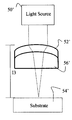
- FIGS. 3 and 4 schematically show how the current invention extends the useful life of lens elements in exposure tools that project high doses of deep UV radiation.
- a light source 50 emits deep UV radiation.
- the lens elements 52 and 56 are substantially aligned in a lens assembly that creates a focal length I 3 .
- First lens element 52 is formed from materials that densify and second lens element 56 is formed from materials that rarefy.
- the lens elements 52 and 56 are arranged in reference to each other to provide a desired focal length I 3 so that the lens elements 52 and 56 focus the light from the light source 50 on the substrate 54 .
- FIG. 4 shows the configuration of FIG. 3 after high dose radiation exposure from light source 50 ′.
- the first lens element 52 ′ densifies.
- the densification causes an increase in the index of refraction, as illustrated in FIG. 2 .
- the distorted wavefront from the first densified lens element 52 ′ passes through a second lens element 56 ′, which rarefies with exposure to deep UV radiation.
- the rarefaction of the second lens element 56 ′ causes a decrease in the index of refraction which corrects for the change in the index of refraction of the first lens element 52 ′.
- the densifying and rarefying lenses are designed such that the volumes change equally but oppositely with increasing exposure to deep UV radiation.
- Conventional optical systems for photolithography exposure tools use lens elements of fused silica (or alternatively calcium fluoride). If a single lens element is used and the material densities, the wavefront is distorted during the exposure process.
- a second lens element 56 , 56 ′ is used in combination with the first lens element 52 , 52 ′.
- the second lens element 56 , 56 ′ is made of excimer-grade fused silica that has been shown empirically to rarefy with exposure to deep UV radiation. Rarefaction of the material of the second lens element 56 , 56 ′ causes the index of refraction to decrease.
- the decreased index of refraction reduces the optical path length, as shown by the dashed lines through lens element 56 ′ of FIG. 4 .
- the combination of the wavefront distortions due to the densification of the first lens element 52 ′ in FIG. 4 and the rarefaction of the second lens element 56 ′ results in a wavefront fully corrected and free of any distortions due to altered indices of refraction.
- the lens assembly of the present invention can be applied in any conventional exposure tool or stepper machine used in semiconductor fabrication to extend the useful lifetime of the illumination or projection lenses.
- the lens elements are incorporated into a projection objective for microlithographic projection exposure systems.
- a schematic of an exposure apparatus utilizing the optical system of the present invention is shown in FIG. 5 .
- a light source 60 emits radiation in the range of less than 300 nm.
- the light source is an ArF excimer laser emitting 193 nm radiation. Radiation from the light source 60 is represented by dashed lines in FIG. 5 .
- the laser radiation is delivered to the mask 68 by the exposure apparatus 70 .
- the exposure apparatus 70 may include any number of components, including fused silica lens elements.
- a first lens element 64 is made of fused silica that densifies with extended exposure to deep UV radiation.
- a second lens element 66 is made of fused silica that rarefies with extended exposure to deep UV radiation.
- the first and second lens elements are made of materials selected to completely compensate for their radiation-induced physical alterations.
- the rarefying lens element 66 increases in volume and the densifying lens element 64 decreases in volume upon exposure to deep UV radiation.
- the thicknesses of the lens elements 64 , 66 are also determined to maximize the compensatory effects with exposure to deep UV radiation.
- the lens elements 64 , 66 are positioned and designed such that lens element 64 incurs higher fluence radiation than does lens element 66 .
- the lens elements 64 , 66 are designed such that their respective indices of refraction change with the same dependence on radiation dose, or alternatively their respective indices of refraction change an appropriate amount such that the lens assembly meets the design specifications throughout the life of the lens assembly.
- the lens elements 64 , 66 may also be arranged such that radiation passes through the rarefying lens element 66 before it is transmitted through the densifying lens element 64 .
- Another embodiment includes positioning a rarefying lens element in a region of high fluence, while a compensating densifying lens element is positioned in a low fluence region of the exposure apparatus.
- an exposure apparatus using the lens assembly of the present invention exposes the mask 68 with a wavefront undistorted by densification effects.
- the mask pattern is projected onto a substrate 72 .
- the materials and design of the fused silica lens elements 64 , 66 are optimized such that the wavefront distortion due to exposure-induced changes in focal length are minimized.
- the lens assembly of this invention is described by the above example, but is not intended to be limited thereby.
- the lens assembly of the present invention could be incorporated into any appropriate component of an exposure apparatus.
- the lens assembly of the present invention may contain a plurality of lens elements and may be in a symmetrical arrangement by design or arranged in groups that are not completely symmetrical.
- Lens assemblies of the present invention may be used in high or low fluence regions or both.
- lens elements may be designed and positioned such that the densifying and rarefying properties of the lens elements receive compensation from the other lens elements in the lens assembly.
- a lens design program can be used to calculate the change in the optical path length based on the appropriate laser energy density illumination over the entire volume of the lens element throughout the entire lifetime of the optical system. Any method used to perform these calculations will account for the changes in the optical path length as well as the changes in the physical thickness of the lens as a result of exposure to the laser irradiation.
- Lens design software such as CODE V and ZEMAX can be used to perform all the design calculations for this embodiment.
- the change in the optical path length for the second lens element 66 is calculated in a similar manner and the calculations account for the optical path length changes caused by a decrease in the index of refraction for this second lens element 66 .
- the lens design program calculates the thickness and surface curvature of each lens element to determine the minimum effect on wavefront deviations throughout the lifetime of the optical system under laser irradiation.
- the calculations may be optimized by a least squares underconstrained optimization of multiple equations with multiple unknowns.
- the optimization is accomplished by iterations of the initial design at periodic intervals throughout the expected lifetime of the lens systems. For example, the expected lifetime of the lens system is between 40-100 billion laser pulses for a ten-year lifetime.
- the optimization may be accomplished by calculating the wavefront change at 1 billion pulse intervals and then optimizing all design aspects over 40 billion pulses.
- Assembly design aspects include, but are not limited to, the lens material, index of refraction, thickness, surface curvature, and lens position.
Abstract
Description
Claims (28)
Priority Applications (1)
| Application Number | Priority Date | Filing Date | Title |
|---|---|---|---|
| US09/603,682 US6339505B1 (en) | 2000-06-26 | 2000-06-26 | Method for radiation projection and lens assembly for semiconductor exposure tools |
Applications Claiming Priority (1)
| Application Number | Priority Date | Filing Date | Title |
|---|---|---|---|
| US09/603,682 US6339505B1 (en) | 2000-06-26 | 2000-06-26 | Method for radiation projection and lens assembly for semiconductor exposure tools |
Publications (1)
| Publication Number | Publication Date |
|---|---|
| US6339505B1 true US6339505B1 (en) | 2002-01-15 |
Family
ID=24416484
Family Applications (1)
| Application Number | Title | Priority Date | Filing Date |
|---|---|---|---|
| US09/603,682 Expired - Fee Related US6339505B1 (en) | 2000-06-26 | 2000-06-26 | Method for radiation projection and lens assembly for semiconductor exposure tools |
Country Status (1)
| Country | Link |
|---|---|
| US (1) | US6339505B1 (en) |
Cited By (14)
| Publication number | Priority date | Publication date | Assignee | Title |
|---|---|---|---|---|
| US20030167798A1 (en) * | 2002-03-05 | 2003-09-11 | Corning Incorporated | Optical members and methods for predicting the performance of optical members and optical systems |
| US20040263811A1 (en) * | 2003-04-24 | 2004-12-30 | Asml Netherlands B.V. | Method of and preventing focal plane anomalies in the focal plane of a projection system |
| US20050140954A1 (en) * | 2003-12-24 | 2005-06-30 | Carl Zeiss Smt Ag | Projection optical system |
| US20060232785A1 (en) * | 2005-04-19 | 2006-10-19 | Regis Grasser | Interferometers of high resolutions |
| US20090201478A1 (en) * | 2004-12-09 | 2009-08-13 | Carl Zeiss Smt Ag | Transmitting optical element and objective for a microlithographic projection exposure apparatus |
| US20100091361A1 (en) * | 2008-10-14 | 2010-04-15 | Canon Kabushiki Kaisha | Projection optical system, exposure apparatus, and device fabrication method |
| US8274743B2 (en) * | 2010-04-08 | 2012-09-25 | Scaggs Michael J | Thermally compensating lens for high power lasers |
| US20130188257A1 (en) * | 2012-01-20 | 2013-07-25 | Samsung Electronics Co., Ltd. | Micro lens, device employing the same, and method of manufacturing the same |
| US11529230B2 (en) | 2019-04-05 | 2022-12-20 | Amo Groningen B.V. | Systems and methods for correcting power of an intraocular lens using refractive index writing |
| US11564839B2 (en) | 2019-04-05 | 2023-01-31 | Amo Groningen B.V. | Systems and methods for vergence matching of an intraocular lens with refractive index writing |
| US11583389B2 (en) | 2019-04-05 | 2023-02-21 | Amo Groningen B.V. | Systems and methods for correcting photic phenomenon from an intraocular lens and using refractive index writing |
| US11583388B2 (en) | 2019-04-05 | 2023-02-21 | Amo Groningen B.V. | Systems and methods for spectacle independence using refractive index writing with an intraocular lens |
| US11678975B2 (en) | 2019-04-05 | 2023-06-20 | Amo Groningen B.V. | Systems and methods for treating ocular disease with an intraocular lens and refractive index writing |
| US11944574B2 (en) | 2019-04-05 | 2024-04-02 | Amo Groningen B.V. | Systems and methods for multiple layer intraocular lens and using refractive index writing |
Citations (10)
| Publication number | Priority date | Publication date | Assignee | Title |
|---|---|---|---|---|
| US4474463A (en) | 1982-08-30 | 1984-10-02 | Tre Semiconductor Equipment Corporation | Mixer coupling lens subassembly for photolithographic system |
| US5170207A (en) | 1990-12-12 | 1992-12-08 | Olympus Optical Co., Ltd. | Projection lens system |
| US5517279A (en) | 1993-08-30 | 1996-05-14 | Hugle; William B. | Lens array photolithography |
| US5616159A (en) * | 1995-04-14 | 1997-04-01 | Corning Incorporated | Method of forming high purity fused silica having high resistance to optical damage |
| US5891605A (en) * | 1996-01-16 | 1999-04-06 | Lucent Technologies Inc. | Reduction in damage to optical elements used in optical lithography for device fabrication |
| US5896222A (en) | 1995-12-22 | 1999-04-20 | Corning Incorporated | Fused silica lens, microlithography system including a fused silica lens and method of making a fused silica lens |
| US5978070A (en) | 1998-02-19 | 1999-11-02 | Nikon Corporation | Projection exposure apparatus |
| US5982558A (en) | 1995-12-27 | 1999-11-09 | Carl-Zeiss-Stiftung | REMA objective for microlithographic projection exposure systems |
| US6087283A (en) * | 1995-01-06 | 2000-07-11 | Nikon Corporation | Silica glass for photolithography |
| US6242136B1 (en) * | 1999-02-12 | 2001-06-05 | Corning Incorporated | Vacuum ultraviolet transmitting silicon oxyfluoride lithography glass |
-
2000
- 2000-06-26 US US09/603,682 patent/US6339505B1/en not_active Expired - Fee Related
Patent Citations (11)
| Publication number | Priority date | Publication date | Assignee | Title |
|---|---|---|---|---|
| US4474463A (en) | 1982-08-30 | 1984-10-02 | Tre Semiconductor Equipment Corporation | Mixer coupling lens subassembly for photolithographic system |
| US5170207A (en) | 1990-12-12 | 1992-12-08 | Olympus Optical Co., Ltd. | Projection lens system |
| US5517279A (en) | 1993-08-30 | 1996-05-14 | Hugle; William B. | Lens array photolithography |
| US6087283A (en) * | 1995-01-06 | 2000-07-11 | Nikon Corporation | Silica glass for photolithography |
| US5616159A (en) * | 1995-04-14 | 1997-04-01 | Corning Incorporated | Method of forming high purity fused silica having high resistance to optical damage |
| US5668067A (en) * | 1995-04-14 | 1997-09-16 | Corning Incorporated | High purity fused silica having high resistance to optical damage |
| US5896222A (en) | 1995-12-22 | 1999-04-20 | Corning Incorporated | Fused silica lens, microlithography system including a fused silica lens and method of making a fused silica lens |
| US5982558A (en) | 1995-12-27 | 1999-11-09 | Carl-Zeiss-Stiftung | REMA objective for microlithographic projection exposure systems |
| US5891605A (en) * | 1996-01-16 | 1999-04-06 | Lucent Technologies Inc. | Reduction in damage to optical elements used in optical lithography for device fabrication |
| US5978070A (en) | 1998-02-19 | 1999-11-02 | Nikon Corporation | Projection exposure apparatus |
| US6242136B1 (en) * | 1999-02-12 | 2001-06-05 | Corning Incorporated | Vacuum ultraviolet transmitting silicon oxyfluoride lithography glass |
Non-Patent Citations (2)
| Title |
|---|
| ArF Laser Induced Absorption in Fused Silica Exposed to Low Fluence at 2000Hz, Optical Microlithography XIV, proceedings of SPIE vol. 4346, Mar. 2, 2001. * |
| Behavior of Fused Silica Under 193nm Irradiation, Technology Transfer # 00073974A-TR, Internatinal SEMATECH, Jul. 25, 2000.* |
Cited By (22)
| Publication number | Priority date | Publication date | Assignee | Title |
|---|---|---|---|---|
| WO2003076912A1 (en) * | 2002-03-05 | 2003-09-18 | Corning Incorporated | Optical members and methods for predicting the performance of optical members and optical systems |
| JP2005519301A (en) * | 2002-03-05 | 2005-06-30 | コーニング インコーポレイテッド | Optical member and method for predicting performance of optical member and optical system |
| US20030167798A1 (en) * | 2002-03-05 | 2003-09-11 | Corning Incorporated | Optical members and methods for predicting the performance of optical members and optical systems |
| US20040263811A1 (en) * | 2003-04-24 | 2004-12-30 | Asml Netherlands B.V. | Method of and preventing focal plane anomalies in the focal plane of a projection system |
| US7068349B2 (en) * | 2003-04-24 | 2006-06-27 | Asml Netherlands B.V. | Method of and preventing focal plane anomalies in the focal plane of a projection system |
| US20050140954A1 (en) * | 2003-12-24 | 2005-06-30 | Carl Zeiss Smt Ag | Projection optical system |
| US6992753B2 (en) | 2003-12-24 | 2006-01-31 | Carl Zeiss Smt Ag | Projection optical system |
| US8570488B2 (en) * | 2004-12-09 | 2013-10-29 | Carl Zeiss Smt Gmbh | Transmitting optical element and objective for a microlithographic projection exposure apparatus |
| US20090201478A1 (en) * | 2004-12-09 | 2009-08-13 | Carl Zeiss Smt Ag | Transmitting optical element and objective for a microlithographic projection exposure apparatus |
| US20060232785A1 (en) * | 2005-04-19 | 2006-10-19 | Regis Grasser | Interferometers of high resolutions |
| US7630085B2 (en) * | 2005-04-19 | 2009-12-08 | Texas Instruments Incorporated | Interferometers of high resolutions |
| US20100091361A1 (en) * | 2008-10-14 | 2010-04-15 | Canon Kabushiki Kaisha | Projection optical system, exposure apparatus, and device fabrication method |
| US8432532B2 (en) * | 2008-10-14 | 2013-04-30 | Canon Kabushiki Kaisha | Projection optical system with rarefaction compensation |
| US8274743B2 (en) * | 2010-04-08 | 2012-09-25 | Scaggs Michael J | Thermally compensating lens for high power lasers |
| US20130188257A1 (en) * | 2012-01-20 | 2013-07-25 | Samsung Electronics Co., Ltd. | Micro lens, device employing the same, and method of manufacturing the same |
| US11529230B2 (en) | 2019-04-05 | 2022-12-20 | Amo Groningen B.V. | Systems and methods for correcting power of an intraocular lens using refractive index writing |
| US11564839B2 (en) | 2019-04-05 | 2023-01-31 | Amo Groningen B.V. | Systems and methods for vergence matching of an intraocular lens with refractive index writing |
| US11583389B2 (en) | 2019-04-05 | 2023-02-21 | Amo Groningen B.V. | Systems and methods for correcting photic phenomenon from an intraocular lens and using refractive index writing |
| US11583388B2 (en) | 2019-04-05 | 2023-02-21 | Amo Groningen B.V. | Systems and methods for spectacle independence using refractive index writing with an intraocular lens |
| US11678975B2 (en) | 2019-04-05 | 2023-06-20 | Amo Groningen B.V. | Systems and methods for treating ocular disease with an intraocular lens and refractive index writing |
| US11931296B2 (en) | 2019-04-05 | 2024-03-19 | Amo Groningen B.V. | Systems and methods for vergence matching of an intraocular lens with refractive index writing |
| US11944574B2 (en) | 2019-04-05 | 2024-04-02 | Amo Groningen B.V. | Systems and methods for multiple layer intraocular lens and using refractive index writing |
Similar Documents
| Publication | Publication Date | Title |
|---|---|---|
| US6829041B2 (en) | Projection optical system and projection exposure apparatus having the same | |
| US6339505B1 (en) | Method for radiation projection and lens assembly for semiconductor exposure tools | |
| JP3413067B2 (en) | Projection optical system and projection exposure apparatus using the same | |
| KR101503992B1 (en) | Exposure method and apparatus, and device manufacturing method | |
| US7073924B2 (en) | Projection exposure apparatus with line width calculator controlled diaphragm unit | |
| US7616290B2 (en) | Exposure apparatus and method | |
| US20070046921A1 (en) | Exposure apparatus and method | |
| US20060197930A1 (en) | Exposure method and apparatus | |
| US20060170889A1 (en) | Exposure Apparatus, Manufacturing Method of Optical Element, and Device Manufacturing Method | |
| KR100291564B1 (en) | Optical member for optical lithography and evaluation method of optical member | |
| TW200525305A (en) | Apparatus for and method of forming optical images and process for manufacturing a device using this method | |
| JP2004502308A (en) | Apparatus and method for compensating critical dimension deviation of photomask | |
| KR20010062343A (en) | Projection exposure apparatus and method of manufacturing a device using the projection exposure apparatus | |
| JP3762323B2 (en) | Exposure equipment | |
| US7242457B2 (en) | Exposure apparatus and exposure method, and device manufacturing method using the same | |
| JP4684563B2 (en) | Exposure apparatus and method | |
| JP5094517B2 (en) | Exposure apparatus, measurement method, stabilization method, and device manufacturing method | |
| JP2009032747A (en) | Scanning stepper and device manufacturing method | |
| US8163467B2 (en) | Dummy light-exposed substrate, method of manufacturing the same, immersion exposure apparatus, and device manufacturing method | |
| US20060055915A1 (en) | Measuring apparatus, test reticle, exposure apparatus and device manufacturing method | |
| US8656319B2 (en) | Optical proximity correction convergence control | |
| JP3632264B2 (en) | X-ray projection exposure apparatus | |
| US20040253549A1 (en) | Device manufacture method | |
| US20080204692A1 (en) | Microlithographic projection exposure apparatus and method for producing microstructured components | |
| JP4503967B2 (en) | Adjustment filter and exposure apparatus |
Legal Events
| Date | Code | Title | Description |
|---|---|---|---|
| AS | Assignment |
Owner name: INTERNATIONAL BUSINESS MACHINES CORPORATION, NEW Y Free format text: ASSIGNMENT OF ASSIGNORS INTEREST;ASSIGNOR:BATES, ALLEN KEITH;REEL/FRAME:010936/0895 Effective date: 20000622 |
|
| FPAY | Fee payment |
Year of fee payment: 4 |
|
| FPAY | Fee payment |
Year of fee payment: 8 |
|
| REMI | Maintenance fee reminder mailed | ||
| LAPS | Lapse for failure to pay maintenance fees | ||
| STCH | Information on status: patent discontinuation |
Free format text: PATENT EXPIRED DUE TO NONPAYMENT OF MAINTENANCE FEES UNDER 37 CFR 1.362 |
|
| FP | Expired due to failure to pay maintenance fee |
Effective date: 20140115 |
|
| AS | Assignment |
Owner name: GLOBALFOUNDRIES U.S. 2 LLC, NEW YORK Free format text: ASSIGNMENT OF ASSIGNORS INTEREST;ASSIGNOR:INTERNATIONAL BUSINESS MACHINES CORPORATION;REEL/FRAME:036550/0001 Effective date: 20150629 |
|
| AS | Assignment |
Owner name: GLOBALFOUNDRIES INC., CAYMAN ISLANDS Free format text: ASSIGNMENT OF ASSIGNORS INTEREST;ASSIGNORS:GLOBALFOUNDRIES U.S. 2 LLC;GLOBALFOUNDRIES U.S. INC.;REEL/FRAME:036779/0001 Effective date: 20150910 |