US6339607B1 - Method and apparatus for modulated integrated optically pumped vertical cavity surface emitting lasers - Google Patents
Method and apparatus for modulated integrated optically pumped vertical cavity surface emitting lasers Download PDFInfo
- Publication number
- US6339607B1 US6339607B1 US09/560,008 US56000800A US6339607B1 US 6339607 B1 US6339607 B1 US 6339607B1 US 56000800 A US56000800 A US 56000800A US 6339607 B1 US6339607 B1 US 6339607B1
- Authority
- US
- United States
- Prior art keywords
- surface emitting
- emitting laser
- cavity surface
- vertical cavity
- laser
- Prior art date
- Legal status (The legal status is an assumption and is not a legal conclusion. Google has not performed a legal analysis and makes no representation as to the accuracy of the status listed.)
- Expired - Fee Related
Links
Images


Classifications
-
- H—ELECTRICITY
- H01—ELECTRIC ELEMENTS
- H01S—DEVICES USING THE PROCESS OF LIGHT AMPLIFICATION BY STIMULATED EMISSION OF RADIATION [LASER] TO AMPLIFY OR GENERATE LIGHT; DEVICES USING STIMULATED EMISSION OF ELECTROMAGNETIC RADIATION IN WAVE RANGES OTHER THAN OPTICAL
- H01S5/00—Semiconductor lasers
- H01S5/04—Processes or apparatus for excitation, e.g. pumping, e.g. by electron beams
- H01S5/041—Optical pumping
-
- H—ELECTRICITY
- H01—ELECTRIC ELEMENTS
- H01S—DEVICES USING THE PROCESS OF LIGHT AMPLIFICATION BY STIMULATED EMISSION OF RADIATION [LASER] TO AMPLIFY OR GENERATE LIGHT; DEVICES USING STIMULATED EMISSION OF ELECTROMAGNETIC RADIATION IN WAVE RANGES OTHER THAN OPTICAL
- H01S5/00—Semiconductor lasers
- H01S5/02—Structural details or components not essential to laser action
- H01S5/026—Monolithically integrated components, e.g. waveguides, monitoring photo-detectors, drivers
-
- H—ELECTRICITY
- H01—ELECTRIC ELEMENTS
- H01S—DEVICES USING THE PROCESS OF LIGHT AMPLIFICATION BY STIMULATED EMISSION OF RADIATION [LASER] TO AMPLIFY OR GENERATE LIGHT; DEVICES USING STIMULATED EMISSION OF ELECTROMAGNETIC RADIATION IN WAVE RANGES OTHER THAN OPTICAL
- H01S5/00—Semiconductor lasers
- H01S5/02—Structural details or components not essential to laser action
- H01S5/0206—Substrates, e.g. growth, shape, material, removal or bonding
- H01S5/0215—Bonding to the substrate
- H01S5/0216—Bonding to the substrate using an intermediate compound, e.g. a glue or solder
-
- H—ELECTRICITY
- H01—ELECTRIC ELEMENTS
- H01S—DEVICES USING THE PROCESS OF LIGHT AMPLIFICATION BY STIMULATED EMISSION OF RADIATION [LASER] TO AMPLIFY OR GENERATE LIGHT; DEVICES USING STIMULATED EMISSION OF ELECTROMAGNETIC RADIATION IN WAVE RANGES OTHER THAN OPTICAL
- H01S5/00—Semiconductor lasers
- H01S5/02—Structural details or components not essential to laser action
- H01S5/026—Monolithically integrated components, e.g. waveguides, monitoring photo-detectors, drivers
- H01S5/0265—Intensity modulators
-
- H—ELECTRICITY
- H01—ELECTRIC ELEMENTS
- H01S—DEVICES USING THE PROCESS OF LIGHT AMPLIFICATION BY STIMULATED EMISSION OF RADIATION [LASER] TO AMPLIFY OR GENERATE LIGHT; DEVICES USING STIMULATED EMISSION OF ELECTROMAGNETIC RADIATION IN WAVE RANGES OTHER THAN OPTICAL
- H01S5/00—Semiconductor lasers
- H01S5/06—Arrangements for controlling the laser output parameters, e.g. by operating on the active medium
- H01S5/0607—Arrangements for controlling the laser output parameters, e.g. by operating on the active medium by varying physical parameters other than the potential of the electrodes, e.g. by an electric or magnetic field, mechanical deformation, pressure, light, temperature
- H01S5/0608—Arrangements for controlling the laser output parameters, e.g. by operating on the active medium by varying physical parameters other than the potential of the electrodes, e.g. by an electric or magnetic field, mechanical deformation, pressure, light, temperature controlled by light, e.g. optical switch
-
- H—ELECTRICITY
- H01—ELECTRIC ELEMENTS
- H01S—DEVICES USING THE PROCESS OF LIGHT AMPLIFICATION BY STIMULATED EMISSION OF RADIATION [LASER] TO AMPLIFY OR GENERATE LIGHT; DEVICES USING STIMULATED EMISSION OF ELECTROMAGNETIC RADIATION IN WAVE RANGES OTHER THAN OPTICAL
- H01S5/00—Semiconductor lasers
- H01S5/06—Arrangements for controlling the laser output parameters, e.g. by operating on the active medium
- H01S5/062—Arrangements for controlling the laser output parameters, e.g. by operating on the active medium by varying the potential of the electrodes
- H01S5/06209—Arrangements for controlling the laser output parameters, e.g. by operating on the active medium by varying the potential of the electrodes in single-section lasers
- H01S5/06216—Pulse modulation or generation
-
- H—ELECTRICITY
- H01—ELECTRIC ELEMENTS
- H01S—DEVICES USING THE PROCESS OF LIGHT AMPLIFICATION BY STIMULATED EMISSION OF RADIATION [LASER] TO AMPLIFY OR GENERATE LIGHT; DEVICES USING STIMULATED EMISSION OF ELECTROMAGNETIC RADIATION IN WAVE RANGES OTHER THAN OPTICAL
- H01S5/00—Semiconductor lasers
- H01S5/06—Arrangements for controlling the laser output parameters, e.g. by operating on the active medium
- H01S5/062—Arrangements for controlling the laser output parameters, e.g. by operating on the active medium by varying the potential of the electrodes
- H01S5/06226—Modulation at ultra-high frequencies
-
- H—ELECTRICITY
- H01—ELECTRIC ELEMENTS
- H01S—DEVICES USING THE PROCESS OF LIGHT AMPLIFICATION BY STIMULATED EMISSION OF RADIATION [LASER] TO AMPLIFY OR GENERATE LIGHT; DEVICES USING STIMULATED EMISSION OF ELECTROMAGNETIC RADIATION IN WAVE RANGES OTHER THAN OPTICAL
- H01S5/00—Semiconductor lasers
- H01S5/10—Construction or shape of the optical resonator, e.g. extended or external cavity, coupled cavities, bent-guide, varying width, thickness or composition of the active region
- H01S5/1082—Construction or shape of the optical resonator, e.g. extended or external cavity, coupled cavities, bent-guide, varying width, thickness or composition of the active region with a special facet structure, e.g. structured, non planar, oblique
- H01S5/1085—Oblique facets
-
- H—ELECTRICITY
- H01—ELECTRIC ELEMENTS
- H01S—DEVICES USING THE PROCESS OF LIGHT AMPLIFICATION BY STIMULATED EMISSION OF RADIATION [LASER] TO AMPLIFY OR GENERATE LIGHT; DEVICES USING STIMULATED EMISSION OF ELECTROMAGNETIC RADIATION IN WAVE RANGES OTHER THAN OPTICAL
- H01S5/00—Semiconductor lasers
- H01S5/10—Construction or shape of the optical resonator, e.g. extended or external cavity, coupled cavities, bent-guide, varying width, thickness or composition of the active region
- H01S5/18—Surface-emitting [SE] lasers, e.g. having both horizontal and vertical cavities
- H01S5/183—Surface-emitting [SE] lasers, e.g. having both horizontal and vertical cavities having only vertical cavities, e.g. vertical cavity surface-emitting lasers [VCSEL]
- H01S5/18308—Surface-emitting [SE] lasers, e.g. having both horizontal and vertical cavities having only vertical cavities, e.g. vertical cavity surface-emitting lasers [VCSEL] having a special structure for lateral current or light confinement
- H01S5/18311—Surface-emitting [SE] lasers, e.g. having both horizontal and vertical cavities having only vertical cavities, e.g. vertical cavity surface-emitting lasers [VCSEL] having a special structure for lateral current or light confinement using selective oxidation
Definitions
- the present invention relates generally to semiconductor lasers. More particularly, the present invention relates to modulation of semiconductor lasers.
- semiconductor lasers have become more important.
- One of the most important applications of semiconductor lasers is in communication systems where fiber optic communication media is employed.
- communication speed has become more important in order to increase data bandwidth in electronic communication systems.
- Improved semiconductor lasers can play a vital roll in increasing data bandwidth in communication systems using fiber optic communication media such as local area networks (LANs), metropolitan area networks (MANs) and wide area networks (WANs).
- LANs local area networks
- MANs metropolitan area networks
- WANs wide area networks
- a preferred component for optical interconnection of electronic components and systems via optical fibers is a semiconductor laser.
- VCSEL vertical cavity surface emitting laser
- VCSELs have been electrically excited (i.e. electrically pumped) by a power supply in order to stimulate photon emission.
- electrically excited i.e. electrically pumped
- achieving photon emission at long wavelengths using electrical pumping has not been commercially successful due to a number of disadvantages.
- a VCSEL can be optically excited (i.e. optically pumped) to stimulate photon emission.
- the laser output needs to be modulated somehow to communicate a signal.
- One type of laser modulation scheme varies the intensity of the light generated by the laser. Oftentimes this has been done externally from the laser, similar to a camera's shutter allowing light to pass through to an unexposed film. However, this requires additional elements. It is more desirable to directly modulate a semiconductor laser.
- direct modulation of semiconductor lasers at the desired high frequencies of communication systems has been limited by jitter and chirping in addition to turn-on delays.
- Turn-on delay is the time it takes for a semiconductor laser to emit photons in response to receiving an electric turn on signal. Jitter refers to the variations in the pulses of emitted photons in relation to a constant pulse train of an electric signal.
- Chirping refers to changes in the wavelengths of the emitted photons from a semiconductor laser.
- the present invention includes methods, apparatus and systems as described in the claims.
- Modulated integrated optically pumped vertical cavity surface emitting lasers are formed by integrating an electrically pumped semiconductor laser and a vertical cavity surface emitting laser (VCSEL) together with a means of direct modulation of the electrically pumped semiconductor laser.
- the electrically pumped semiconductor laser is a type of folded cavity surface emitting laser (FCSEL).
- FCSEL folded cavity surface emitting laser
- the FCSEL is partitioned into two sections by a gap in material layers. In these embodiments, one section of the FCSEL is biased so as to maintain the generation of photons without causing the optically pumped VCSEL to lase while the second section of the FCSEL is used for modulation and causes the optically pumped VCSEL to lase.
- an electric-absorption modulator is sandwiched between an electrically pumped FCSEL and an optically pumped VCSEL.
- the electric-absorption modulator acts similar to a camera shutter and allows photons to pass through from the electrically pumped FCSEL to the optically pumped VCSEL when in one state and blocks photons from reaching the optically pumped VCSEL when in another state.
- FIG. 1A is a magnified side view of an integrated optically pumped vertical cavity surface emitting laser.
- FIG. 1B is a magnified cross-sectional front view of the integrated optically pumped vertical cavity surface emitting laser of FIG. 1 A.
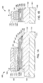
- FIG. 2A is a magnified side view of a first embodiment of the modulated integrated optically pumped VCSEL of the present invention.
- FIG. 2B is a magnified side view of a second embodiment of the modulated integrated optically pumped VCSEL of the present invention.
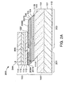
- FIG. 3A is a magnified cross-sectional view of a third embodiment of the modulated integrated optically pumped VCSEL of the present invention.
- FIG. 3B is a magnified back side view of the integrated optically pumped vertical cavity surface emitting laser of FIG. 3 A.
- FIG. 4 is a magnified side view of a fourth embodiment of the modulated integrated optically pumped VCSEL of the present invention.
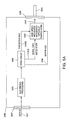
- FIG. 5A is a block diagram of a system for modulating the modulated integrated optically pumped VCSELs of FIG. 2A, FIG. 2B, and FIGS. 3A-3B.
- FIG. 5B is a block diagram of a system for modulating the modulated integrated optically pumped VCSEL of FIG. 4 .
- an optically pumped long wavelength vertical cavity surface emitting laser seems to be the preferable type of semiconductor laser.
- a VCSEL that is optically pumped need not be doped to lase. Therefore an optically pumped VCSEL need not have its high frequency operation limited by parasitic capacitance and inductance caused by dopants and metal contact pads that would otherwise have been added.
- the only high frequency limits of an optically pumped VCSEL would be as a result of its intrinsic carrier transport time and thermionic emission.
- the high frequency limits due to intrinsic carrier transport time and thermionic emission do not usually take effect until modulation frequencies of twenty giga-Hertz (20 GHz) or more are reached.
- VCSEL emission frequency is strongly confined by its high cavity-Q and cavity resonance, and thus laser modulation chirping is not as pronounced as an electrically pumped conventional in-plane semiconductor laser. Therefore, an optically pumped VCSEL has greater commercial potential for operation at high frequencies of modulation.
- the present invention In order to modulate an optically pumped VCSEL at high frequencies, the present invention directly modulates the pump laser, which in turn modulates the optically pumped VCSEL. To minimize the turn-on delay and pulse jitter, the present invention pre-biases the optically pumped VCSEL just above its threshold to ensure the maximum extinction ratio.
- the extinction ratio In NRZ (non-return-to-zero) modulation, the extinction ratio (ER) is the ratio of the power output of photons in a data-on state input to the power output of photons in a data-off state input. In communications systems, a larger ER is preferred but it is usually difficult to achieve due to poor laser performance.
- the threshold of an optically pumped VCSEL is the input optical pump power needed for the VCSEL to reach lasing threshold. With an optically pumped VCSEL being close to its threshold level, the power output of photons from it corresponding to the data-off state is very low. Thus the ER can be very large with the optically pumped VCSEL in this condition. To accomplish this, the present invention maintains a minimum pump laser power output level just above the VCSEL threshold power level. Modulating the pump laser well beyond its own threshold current level reduces jitter and the turn-on delay becomes negligible. Additionally, any chirping of the pump laser from modulation will have a minimal impact on the optically pumped VCSEL. This is so because the optically pumped VCSEL is insensitive to wavelength variations of photons generated by the pump laser.
- a limiting factor of the pump laser that effects the optically pumped VCSEL is the parasitics of the pump laser.
- Parasitics such as resistance, capacitance and inductance, tend to limit the achievable direct modulation frequency of the electrically pumped laser, which in turn can impact the direct modulation frequency of the long wavelength VCSEL.
- the present invention substantially reduces the problem posed by parasitics.
- the pump laser has two sectional areas. One of the two sectional areas is always biased with a current so as to keep the pump laser turned on. This one sectional area is always sufficiently biased by a current to keep the optically pumped VCSEL just at its lasing threshold.
- the second of the two sectional areas is used to modulate the pump laser, which in turn modulates the optically pumped VCSEL.
- Splitting the pump laser into two sectional areas partitions the parasitics so that a lower level of parasitics in the pump laser need only be modulated.
- an electric-absorption (EA) modulator is used to modulate the light or photons generated by the pump laser before being coupled into the optically pumped VCSEL.
- the parasitics associated with modulating the electric-absorption (EA) modulator are minimal such that modulation of the optically pumped VCSEL can occur at high frequencies.
- the present invention provides a modulated integrated optically pumped VCSEL, which is optically pumped by an electrically pumped folded cavity surface emitting laser (FCSEL).
- the modulated integrated optically pumped VCSEL can be modulated at high frequencies and is preferably formed to generated photons of relatively long wavelengths.
- the FCSEL is electrically pumped and its photon output modulated in order to modulate the optically pumped VCSEL at high speeds.
- the integrated optically pumped vertical cavity surface emitting laser (VCSEL) is formed by integrating the electrically pumped FCSEL with an optically pumped VCSEL.
- the FCSEL is designed to emit photons of relatively short wavelengths while the optically pumped VCSEL is designed to emit photons of relatively long wavelengths.
- the electrically pumped FCSEL and optically pumped VCSEL can be integrated together in a number of ways including atomic bonding, wafer bonding, metal bonding, epoxy glue or other well known semiconductor bonding techniques.
- a number of embodiments of the modulated integrated optically pumped VCSEL are disclosed.
- the electrically pumped FCSEL is preferably designed to operate at relatively short wavelengths (from 770 nanometers (nm) to 1100 nanometers (nm)) with an optically pumped VCSEL designed to operate preferably at relatively long wavelengths (from 1250 nm to 1700 nm).
- the optically pumped VCSEL operates without the use of electric power by being optically pumped by the electrically pumped FCSEL. Integration of the lasers depends upon the type of semiconductor materials utilized in forming the two lasers.
- the two lasers are integrated into one unit through semiconductor processing methods such as monolithic epitaxial growth or by joining outer layers of the two lasers together through atomic bonding, wafer bonding, metal bonding, epoxy glue or other well known semiconductor bonding techniques.
- the optically pumped VCSEL can be bonded to the FCSEL at an angle in order to avoid reflected light from the long wavelength VCSEL being directly returned to the in-plane laser to thereby avoiding optical noise being fed back into the FCSEL.
- a third laser can also be used to generate a small spot pump beam to couple to the optically pumped VCSEL in order to gain guide photons to emit at a single mode transversely.
- the electrically pumped FCSEL also referred to as the pump laser
- the output from the optically pumped VCSEL is single mode longitudinally.
- the output from the optically pumped VCSEL can be single mode transversely depending upon the geometric integration scheme and patterning.
- the optically pumped VCSEL operate in a single transverse mode to optimally couple with a single mode fiber. Modulation of the optically pumped VCSEL can be achieved through direct electrical modulation of the pump laser or an electric-absorption modulator.
- the integrated optically pumped VCSEL 100 includes a folded cavity surface emitting laser (FCSEL) 140 integrated with an optically pumped VCSEL 150 .
- the folded cavity surface emitting laser 140 includes a substrate 101 , a distributed Bragg reflector (DBR) 102 , an active area 104 , a confinement layer 105 , a cladding layer 106 , a semiconductor contact layer 107 , a first metal layer as a top contact terminal 108 , a second metal layer as a base terminal 110 , and the facets or beam steering elements 111 A and 111 B.
- DBR distributed Bragg reflector
- Substrate 101 of the FCSEL 104 is preferably an n-type doped Gallium-Arsenide (GaAs) layer.
- the substrate 101 can be a layer of an n-type doped Indium-Phosphide (InP) or other semiconductor materials.
- the DBR 102 is preferably doped to match the substrate 101 .
- the substrate 101 is an n-type doped Indium-Phosphide (InP) or Gallium-Arsenide (GaAs) substrate
- the DBR 102 is n-type doped as well.
- the layers of the DBR 102 are preferably formed from n-type Al x Ga 1 ⁇ x As/Al y Ga 1 ⁇ y As pairs of material with x ranging from 0 and 0.5, and y ranging from 0.5 and 1 for a GaAs substrate.
- the number of pairs may range from as few as five to as many as forty with the typical number of pairs being about twenty pairs of layers.
- an Indium-Aluminum-Gallium-Arsenide/Indium-Phosphide InAlGaAs/InP) distributed Bragg Reflector (DBR)
- DBR distributed Bragg Reflector
- Indium-Gallium-Arsenide-Phosphide/Indium-Phosphide InGaAsP/InP
- other monolithic grown DBR mirror can be grown onto the substrate 101 if it is an InP substrate.
- a Gallium-Arsenide/Aluminum-Gallium-Arsenide (GaAs/AlGaAs) distributed Bragg reflector (DBR) or a dielectric DBR can be bonded to the substrate 101 and the active area 104 .
- the substrate 101 is preferably GaAs.
- Exemplary dielectric materials for a dielectric DBR include titanium di-oxide (TiO 2 ), silicon di-oxide (SiO 2 ), and silicon nitrogen di-oxide (SiNO 2 ).
- the active area 104 can be a Gallium-Arsenide (GaAs), an Aluminum-Gallium-Arsenide (AlGaAs), or an Indium-Gallium-Arsenide (InGaAs) quantum well structure.
- the active area 104 of the FCSEL 140 in the preferred embodiment is a GaAs quantum well structure.
- the quantum well structure can be formed of a single quantum well or multiple quantum wells but in the preferred embodiment one to three quantum wells are utilized.
- the cladding layer 106 of the FCSEL 140 is a p-type GaAs and can alternately be a p-type AlGaAs layer.
- the confinement layer 105 of the FCSEL 140 is preferably an Aluminum-Gallium-Arsenide (AlGaAs) layer with aluminum content at larger than 90% and preferably larger than 95%.
- the Aluminum-Gallium-Arsenide (AlGaAs) layer 105 is formed within a part of the cladding 106 to allow lateral oxidation during device fabrication.
- the confinement layer 105 is formed by oxidizing a portion of an Aluminum-Arsenide (AlAs) layer into an Aluminum-Oxide (Al 2 O 3 ) region.
- the confinement layer 105 provides both current confinement and optical confinement for the FCSEL 140 . Referring momentarily to FIG. 1B, the confinement layer 105 is oxidized to form a narrow conductive stripe above the active region 104 as illustrated.
- the semiconductor contact layer 107 is provided so as to make an ohmic contact to the metal layer of the top contact terminal 108 deposited on its top surface.
- the semiconductor contact layer 107 is preferably a Gallium-Arsenide (GaAs) layer highly doped to be p-type semiconductor so as to provide an ohmic contact.
- GaAs Gallium-Arsenide
- the first metal layer of the top contact terminal 108 forms a first terminal of the integrated optically pumped VCSEL 100 .
- the metal layer for the top contact terminal 108 is only left deposited in certain areas of the semiconductor contact layer 107 so as not to block areas where photons are emitted or interfere with the coupling to the optically pumped VCSEL 150 .
- the second metal layer for the base terminal 110 is deposited on the bottom surface of the substrate 101 in order to form the second terminal of the integrated optically pumped VCSEL 100 .
- the FCSEL 100 is an electrically pumped semiconductor laser which has a folded laser cavity provided by a pair facets (also referred to as reflectors or beam steering elements) 111 A and 111 B at opposite ends.
- the external-angled beam steering element 111 B and the internal-angled beam steering element 111 A are approximately forty five degree angles with the incident light to form the folded cavity of the folded cavity surface emitting laser 140 .
- the beam steering elements 111 A and 111 B are preferably parallel to each other and formed by cleaving, etching, ion milling or other well known semiconductor process.
- the active area 104 of the FCSEL has the external-angled beam steering element 111 B and the internal-angled beam steering element 111 A formed from processing its material layers.
- the external-angled beam steering element 111 B and the internal-angled beam steering element 111 A may continue and be formed into the cladding 106 , the contact layer 107 , and a portion 103 of the DBR 102 as illustrated in the Figures.
- a dielectric coating (not shown) may be added to the facets 111 A and 111 B to act as a mirror coating to increase the reflectivity efficiency or as a surface passivation.
- the layers of materials are first deposited or grown from the beginning layer of the substrate 101 .
- the facets 101 A and 101 B can be formed.
- the facets 101 A and 101 B are formed by cleaving, etching, ion milling or other semiconductor process to remove material.
- the second DBR 116 can be an Al x Ga 1 ⁇ x As/Al y Ga 1 ⁇ y As DBR, an InGaAsP/InP DBR or a dielectric DBR, and is preferably made of pairs of InGaAsP/InP.
- the substrate 118 of the optically pumped VCSEL 150 can be a layer of GaAs or of Indium-Phosphide (InP), and is preferably an InP substrate.
- DBRs 112 and 116 are preferably made of thicknesses to provide substantial (preferably 99% or more) reflection of long wavelengths at 1.3 um or 1.55 um to amplify and stimulate emission. In FIGS.
- the folded cavity surface emitting laser 140 and the optically pumped VCSEL 150 are integrated together at the interface 120 by either fusing, gluing, metal bonding, epoxy bonding or other well-known semiconductor bonding methods.
- interface 120 represents the joining of the surfaces and a layer of material, if any, to join the surfaces.
- the interface 120 can alternately be an air gap in the case where the FCSEL 140 and the optically pumped VCSEL 150 are held mechanically aligned together.
- the folded cavity surface emitting laser 140 generates a short wavelength laser beam 109 which is reflected between the beam steering element 111 A, beam steering element 111 B, DBR 102 , and the contact layer 107 as the laser beam elements 109 A, 109 B and 109 C.
- the in-plane laser beam 109 A is reflected by beam steering element 111 A into the substantially perpendicular beam 109 B for coupling into the VCSEL 150 to optically pump it.
- the optically pumped VCSEL 150 emits photons 144 preferably of a relatively long wavelength as a laser beam.
- the modulated integrated optically pumped VCSEL 200 includes the VCSEL 150 and a two-section FCSEL 140 ′. But for those described below, the elements of optically pumped VCSEL 150 are the same as those described with reference to FIGS. 1A-1B and are not repeated here.
- the two-section FCSEL 140 ′ is similar to FCSEL 140 except that the two-section FCSEL 140 ′ is separated into two sections, a first section 201 and a second section 202 by a gap 205 .
- the gap 205 may be an airgap or a gap filed with an insulative or dielectric material.
- the gap 205 separates the semiconductor contact layer 107 of FCSEL 140 into two sections, semiconductor contact layer 207 A and semiconductor contact layer 207 B of FCSEL 140 ′ in FIG. 2 A.
- Each of the sections 201 and 202 also has its own separate contact terminal, first contact terminal 208 A and second contact terminal 208 B respectively, which are formed out of a deposited metal layer in the desired contact area.
- the separate contact terminals 208 A and 208 B provide for separate control of the FCSEL 140 ′.
- the gap 205 essentially forms two separate sections, first section 201 and second section 202 , of the FCSEL 140 ′.
- the first section 201 of the FCSEL 140 ′ is separately controlled by the first contact terminal 208 A.
- the second section 202 of the FCSEL 140 ′ is separately controlled by the second contact terminal 208 B.
- Interface 120 ′ couples FCSEL 140 ′ to the VCSEL 150 and is formed similarly to interface 120 of FIGS. 1A-1B but for the gap 205 .
- the second section 202 of the FCSEL 140 ′ is DC biased, while the first section 201 of the FCSEL 140 ′ is modulated by data at a data rate, or alternatively the first section 201 can be DC biased while the second section 202 is modulated by data at a data rate.
- the two sections, the first section 201 and the second section 202 are controlled in such a way that the FCSEL 140 ′ is always “on” and generating photons at one power level.
- the second section 202 is controlled so that the pump power of the FCSEL 140 ′ generates photons having a power level at or slightly above the lasing threshold of the optically pumped VCSEL 150 .
- the second section 202 in this case is said to be at a threshold biased state.
- VCSEL 150 does not lase or minimally lases with emitted photons 244 being of a low power level and therefore can be considered turned “off”.
- the combined pump power from the first section 201 and the second section 202 of the FCSEL 140 ′ generate photons of a second power level exceeding the threshold pump power of the VCSEL 150 so that it lases and emits photons 244 .
- VCSEL 150 can be considered turned “on” when it lases and emits photons 244 .
- Optically pumped VCSEL 150 is preferably a long wavelength optically pumped VCSEL to generate photons 244 at a relatively long wavelength such as 1300 nm.
- the elements of the optically pumped VCSEL 150 are the same as those described with respect to FIGS. 1A-1B and are not repeated here.
- FIG. 2B a magnified side view of a modulated integrated optically pumped VCSEL 200 ′ is illustrated.
- the modulated integrated optically pumped VCSEL 200 ′ of FIG. 2B is similar to the modulated integrated optically pumped VCSEL 200 of FIG. 2A except that an unnecessary portion of the optically pumped VCSEL 150 is removed.
- Optically pumped VCSEL 150 ′ is smaller that the optically pumped VCSEL 150 and utilizes semiconductor materials more efficiently.
- the modulated integrated optically pumped VCSEL 200 ′ can have a larger surface contact for the metal contact terminal 208 B.
- VCSEL 200 ′ retains the gap 205 to split the FCSEL 140 ′ into two sections, the first section 201 and the second section 202 .
- gap 205 may be larger or formed differently due to the fact the portion of the optically pumped VCSEL 150 ′ is not covering the gap as in FIG. 2 A.
- a data modulated waveform is coupled into the first contact terminal 208 A to modulate the FCSEL 140 ′ and thereby modulate the optically pumped VCSEL 150 to emit photons 244 or not emit photons 244 .
- a threshold bias signal is coupled into the second contact terminal 208 B while a reference level is coupled into the base terminal 110 . While a voltage waveform is supplied between the first contact terminal 208 A and the base terminal 110 and between the second contact terminal 208 B and the base terminal 110 , currents generated thereby in the FCSEL 140 ′ actually form the threshold bias and modulate the FCSEL 140 ′ into the emission of high or low energy photons into the optically pumped VCSEL 150 .
- FIG. 3A a magnified cross-sectional side view of a modulated integrated optically pumped VCSEL 300 is illustrated.
- the modulated integrated optically pumped VCSEL 300 includes a FCSEL 140 ′′ and the optically pumped VCSEL 150 as illustrated in FIGS. 3A-3B.
- the material layers of the modulated integrated optically pumped VCSEL 300 of FIGS. 3A-3B are the same as those of the integrated optically pumped VCSEL 100 unless discussed below and are otherwise not repeated here for brevity.
- a wafer of optically pumped VCSELs 150 and a wafer of FCSELs 140 are initially formed in the manufacture of the modulated integrated optically pumped VCSEL 300 and joined together.
- portions of material layers are removed.
- the substrate 101 (not shown in FIG. 3A) used to initially form the FCSEL 140 ′′ is removed from the VCSEL 300 .
- a portion of the DBR 102 of the FCSEL is removed, including a gap 305 , to form a first DBR section 312 A and a second DBR section 312 B.
- wafer boding is used to join together in alignment, the optically pumped VCSELs 150 in a wafer format with the FCSELs 140 in a wafer format.
- the device fabrication process of the modulated integrated optically pumped VCSELs 300 starts from the exposed substrate 101 of the FCSELs 140 in the joined wafers. First the substrate 101 is removed and a portion of the DBR 102 of the FCSELs is removed, including a gap 305 , to form a first DBR section 312 A and a second DBR section 312 B of the FCSELs 140 ′′.
- a metal layer is then deposited in two desired contact terminal areas onto the first DBR section 312 A and the second DBR section 312 B to form a first contact terminal 310 A and a second contact terminal 310 B.
- FCSEL side of the joined wafers sufficient portions of FCSEL material layers are etched away to expose an area of the semiconductor contact layer 107 for making p-type electrical contact from the same side as the n-type metal contacts.
- a metal layer is then deposited onto desired areas of the semiconductor contact layer 107 to form the p-contact terminal 308 and the DBR sections 312 A and 312 B to form the n-contact terminals 310 A and 310 B respectively.
- the p-contact terminal 308 couples to the semiconductor contact layer 107 and the n-contact terminal 310 B couples to the DBR section 312 B as illustrated.
- the p-contact terminal 308 extends across the first section 301 and the second section 302 of the FCSEL 140 ′′.
- FCSEL 140 ′′ is a sectional FCSEL having the first section 301 and the second section 302 formed by the gap 305 .
- the gap 305 may be an airgap or a gap filed with an insulative or dielectric material.
- the gap 305 separates the DBR 102 of FCSEL 140 into two sections, a first DBR section 312 A and a second DBR section 312 B of the FCSEL 140 ′′.
- Each of the DBR sections 312 A and 312 B also has its own separate metal contact terminal, first contact terminal 310 A and second contact terminal 310 B respectively, which are formed out of a deposited metal layer in the desired contact area.
- the separate contact terminals 310 A and 310 B provide for separate control of the FCSEL 140 ′′.
- the first section 301 of the FCSEL 140 ′′ is separately controlled by the first contact terminal 310 A.
- the second section 302 of the FCSEL 140 ′′ is separately controlled by the second contact terminal 310 B.
- the second section 302 of the FCSEL 140 ′′ is DC biased, while the first section 301 of the FCSEL 140 ′′ is modulated by data at a data rate, or alternatively the first section 301 can be DC biased while the second section 302 is modulated by data at a data rate.
- the first section 301 and the second section 302 are controlled in such a way that the FCSEL 140 ′′ is always “on” and generating photons but not necessarily at the same power level.
- the second section 302 is controlled so that the pump power of the FCSEL 140 ′′ generates photons having a power level at the lasing threshold of the optically pumped VCSEL 150 .
- the second section 302 is said to be at a threshold biased state.
- VCSEL 150 does not lase or minimally lases with emitted photons 344 being of a low power level and therefore can be considered turned “off”.
- the combined pump power from the first section 301 and the second section 302 of the FCSEL 140 ′′ is at a level exceeding the threshold pump power of the VCSEL 150 so that it lase and emits photons 344 .
- VCSEL 150 can be considered turned “on” when it lases and emits photons 344 .
- a data modulated waveform is coupled into the first contact terminal 310 A to modulate the FCSEL 140 ′′ and thereby modulate the optically pumped VCSEL 150 to emit photons 344 or not emit photons 344 .
- a threshold bias signal is coupled into the second contact terminal 310 B while a reference level is coupled into the contact terminal 308 . While a voltage or current waveform is supplied between the first contact terminal 310 A and the contact terminal 308 and between the second contact terminal 310 B and the contact terminal 308 , currents generated thereby in the FCSEL 140 ′′ actually form the threshold bias and modulate the FCSEL 140 ′′ into the emission of high or low energy photons into the optically pumped VCSEL 150 .
- the pump laser is split into two sections.
- FCSEL 140 ′ is split into the first section 201 and the second section 202 by a gap 205 .
- FCSEL 140 ′′ is split into the first section 301 and the second section 302 .
- the parasitics as seen from the point of view of the electrical connections to the pump laser are also split in two. As a result, the dynamic parasitics associated with data modulation of the first section 201 through the first contact terminal 208 A and of the first section 301 through the first contact terminal 310 A are reduced from that of modulating the top contact terminal 108 of FIGS.
- the dynamic parasitic reduction at the first contact terminal 208 A is because only a small section of the pump FCSEL 140 ′, the first section 201 , needs to be modulated.
- the dynamic parasitic reduction at the first contact terminal 310 A is because only a small section of the pump FCSEL 140 ′′, the first section 301 , needs to be modulated.
- the modulated integrated optically pumped VCSEL 400 which is the preferred embodiment includes an electrically pumped surface emitting laser, the optically pumped VCSEL 150 and a surface integrated electric-absorption (EA) modulator 405 sandwiched there-between along with the interface 120 ′′′.
- the electrically pumped surface emitting laser can be an electrically pumped inplane surface emitting laser, an electrically pumped grating surface emitting laser, an electrically pumped VCSEL, or an electrically pumped FCSEL 140 as shown in FIG. 4 .
- the elements of the material layers of the FCSEL 140 and the VCSEL 150 of the modulated integrated optically pumped VCSEL 400 are the same as those described with reference to FIGS. 1A-1B and are not repeated herein for brevity.
- the electric-absorption (EA) modulator 405 is formed of multiple quantum wells sandwiched between cladding layers and contact layers.
- the optically pumped VCSEL 150 is coupled to the EA modulator 405 through the interface 120 ′′′.
- Interface 120 ′′′ is formed similarly to interface 120 of FIGS. 1A-1B.
- the EA modulator 405 couples to the semiconductor contact layer 107 of the electrically pumped FCSEL 140 .
- the EA modulator 405 is used to modulate the light or photons generated by the electrically pumped FCSEL 140 before they are coupled into the optically pumped VCSEL 150 .
- the EA modulator 405 acts similar to a shutter of a still camera.
- the parasitics associated with modulating the EA modulator 405 are minimal such that modulation of the optically pumped VCSEL can occur at high frequencies.
- the EA modulator 405 inherently has chirping but does not effect the optically pumped VCSEL 150 .
- the optically pumped VCSEL 150 is relatively insensitive to variations of the input pump wavelength.
- the EA modulator 405 may have a poor extinction ratio of photons but this does not pose a problem for the modulated integrated optically pumped VCSEL 400 . This is because it is not necessary to completely turn off the electrically pumped FCSEL 140 during an “off” state in order that photons 444 are not emitted.
- FIG. 5A a block diagram of a system 500 for modulation of the embodiments of the modulated integrated optically pumped VCSELs 200 , 200 ′, and 300 is illustrated.
- the system 500 receives a data input 501 through an electronic interface 502 such as a wire, cable, or pins.
- an optical interface 503 such as a collimating lens or fiber pigtail, the system 500 couples to an optical fiber 504 .
- Drive circuitry 506 generates the proper drive currents for a serial data modulation signal 510 A and a threshold bias signal 510 B with respect to the reference 508 .
- System 500 ′ for modulation of the preferred embodiment of the modulated integrated optically pumped VCSEL 400 is illustrated.
- System 500 ′ is similar to system 500 but for drive circuitry 506 ′ which generates a varying voltage between the serial data modulation terminals 410 and 408 of the EA modulator 405 .
- the drive circuitry 506 ′ also provides a voltage or current across terminals 408 and 110 for the FCSEL 140 of the modulated integrated optically pumped VCSEL 400 .
- the turn-on delay was minimized by maintaining the pump laser, the electrically pumped FCSEL, in a biased state generating photons with its power at or slightly above the optically pumped VCSEL threshold. Jitter is minimized in the embodiments as well for this same reason because the pump laser, the electrically pumped FCSEL, is maintained in a biased state constantly generating photons. Chirping was minimized in the embodiments of modulated integrated optically pumped VCSELs 200 , 200 ′, 300 and 400 because the VCSEL is relatively insensitive to the pump wavelength variation.
- the present invention has many advantages over the prior art.
- One advantage of the present invention is that dynamic modulation parasitics are reduced so that modulation frequencies can be greater.
- Another advantage is that modulated integrated optically pumped VCSEL can be commercially manufactured.
- Other advantages of the present invention will become obvious to those of ordinary skill in the art after thoroughly reading this disclosure.
Abstract
Description
Claims (66)
Priority Applications (5)
| Application Number | Priority Date | Filing Date | Title |
|---|---|---|---|
| US09/560,008 US6339607B1 (en) | 1999-10-29 | 2000-04-27 | Method and apparatus for modulated integrated optically pumped vertical cavity surface emitting lasers |
| AU24703/01A AU2470301A (en) | 1999-10-29 | 2000-10-24 | Modulated integrated optically pumped vertical cavity surface emitting lasers |
| PCT/US2000/041517 WO2001031756A1 (en) | 1999-10-29 | 2000-10-24 | Modulated integrated optically pumped vertical cavity surface emitting lasers |
| US09/833,368 US6347108B2 (en) | 1999-10-29 | 2001-04-12 | Method and apparatus for modulated integrated optically pumped vertical cavity surface emitting lasers |
| US10/032,841 US6553048B2 (en) | 1999-10-29 | 2001-10-24 | Modulated integrated optically pumped vertical cavity surface emitting lasers |
Applications Claiming Priority (2)
| Application Number | Priority Date | Filing Date | Title |
|---|---|---|---|
| US09/430,570 US6424669B1 (en) | 1999-10-29 | 1999-10-29 | Integrated optically pumped vertical cavity surface emitting laser |
| US09/560,008 US6339607B1 (en) | 1999-10-29 | 2000-04-27 | Method and apparatus for modulated integrated optically pumped vertical cavity surface emitting lasers |
Related Parent Applications (1)
| Application Number | Title | Priority Date | Filing Date |
|---|---|---|---|
| US09/430,570 Continuation-In-Part US6424669B1 (en) | 1999-10-29 | 1999-10-29 | Integrated optically pumped vertical cavity surface emitting laser |
Related Child Applications (2)
| Application Number | Title | Priority Date | Filing Date |
|---|---|---|---|
| US09/833,368 Division US6347108B2 (en) | 1999-10-29 | 2001-04-12 | Method and apparatus for modulated integrated optically pumped vertical cavity surface emitting lasers |
| US10/032,841 Division US6553048B2 (en) | 1999-10-29 | 2001-10-24 | Modulated integrated optically pumped vertical cavity surface emitting lasers |
Publications (1)
| Publication Number | Publication Date |
|---|---|
| US6339607B1 true US6339607B1 (en) | 2002-01-15 |
Family
ID=23708114
Family Applications (4)
| Application Number | Title | Priority Date | Filing Date |
|---|---|---|---|
| US09/430,570 Expired - Fee Related US6424669B1 (en) | 1999-10-29 | 1999-10-29 | Integrated optically pumped vertical cavity surface emitting laser |
| US09/560,008 Expired - Fee Related US6339607B1 (en) | 1999-10-29 | 2000-04-27 | Method and apparatus for modulated integrated optically pumped vertical cavity surface emitting lasers |
| US10/175,338 Expired - Fee Related US6580741B2 (en) | 1999-10-29 | 2002-06-18 | Systems with integrated optically pumped vertical cavity surface emitting lasers |
| US10/231,592 Expired - Fee Related US6940885B1 (en) | 1999-10-29 | 2002-08-30 | Systems, methods, and apparatuses for optically pumped vertical cavity surface emitting laser devices |
Family Applications Before (1)
| Application Number | Title | Priority Date | Filing Date |
|---|---|---|---|
| US09/430,570 Expired - Fee Related US6424669B1 (en) | 1999-10-29 | 1999-10-29 | Integrated optically pumped vertical cavity surface emitting laser |
Family Applications After (2)
| Application Number | Title | Priority Date | Filing Date |
|---|---|---|---|
| US10/175,338 Expired - Fee Related US6580741B2 (en) | 1999-10-29 | 2002-06-18 | Systems with integrated optically pumped vertical cavity surface emitting lasers |
| US10/231,592 Expired - Fee Related US6940885B1 (en) | 1999-10-29 | 2002-08-30 | Systems, methods, and apparatuses for optically pumped vertical cavity surface emitting laser devices |
Country Status (6)
| Country | Link |
|---|---|
| US (4) | US6424669B1 (en) |
| EP (1) | EP1232547A1 (en) |
| JP (1) | JP2003513477A (en) |
| AU (1) | AU7051100A (en) |
| TW (1) | TW523970B (en) |
| WO (1) | WO2001033678A1 (en) |
Cited By (31)
| Publication number | Priority date | Publication date | Assignee | Title |
|---|---|---|---|---|
| US20020122615A1 (en) * | 2000-12-21 | 2002-09-05 | Painter Oskar J. | Multi-layer dispersion-engineered waveguides and resonators |
| US20030007538A1 (en) * | 1999-10-29 | 2003-01-09 | Wenbin Jiang | Systems with integrated optically pumped vertical cavity surface emitting lasers |
| US20030012246A1 (en) * | 2001-07-12 | 2003-01-16 | Klimek Daniel E. | Semiconductor zigzag laser and optical amplifier |
| US6556610B1 (en) * | 2001-04-12 | 2003-04-29 | E20 Communications, Inc. | Semiconductor lasers |
| US20030081902A1 (en) * | 2001-10-30 | 2003-05-01 | Blauvelt Henry A. | Optical junction apparatus and methods employing optical power transverse-transfer |
| US20030152125A1 (en) * | 2002-02-13 | 2003-08-14 | Junichi Kinoshita | Surface emitting laser and semiconductor light emitting device |
| US6611544B1 (en) | 2000-04-11 | 2003-08-26 | E20 Communications, Inc. | Method and apparatus for narrow bandwidth distributed bragg reflector semiconductor lasers |
| US6625195B1 (en) | 1999-07-20 | 2003-09-23 | Joseph Reid Henrichs | Vertical cavity surface emitting laser that uses intracavity degenerate four wave mixing to produce phase-conjugated and distortion free collimated laser light |
| EP1347322A2 (en) * | 2002-03-22 | 2003-09-24 | Agilent Technologies, Inc. | Producing modulated light using an integrated module |
| US20030235369A1 (en) * | 2001-11-23 | 2003-12-25 | Grosjean Charles I. | Alignment apparatus and methods for transverse optical coupling |
| US20040022289A1 (en) * | 2002-08-01 | 2004-02-05 | Corzine Scott W. | Integrated laser and electro-absorption modulator with improved extinction |
| US6717964B2 (en) * | 2001-07-02 | 2004-04-06 | E20 Communications, Inc. | Method and apparatus for wavelength tuning of optically pumped vertical cavity surface emitting lasers |
| US20040066826A1 (en) * | 2001-12-13 | 2004-04-08 | Emmanuel Picard | Micro-cavity light emitting device and method for making same |
| US20040129935A1 (en) * | 2002-10-10 | 2004-07-08 | Blauvelt Henry A. | Semiconductor photodetector with internal reflector |
| US6798804B2 (en) * | 2000-02-09 | 2004-09-28 | Fuji Photo Film Co., Ltd. | Laser apparatus including surface-emitting semiconductor excited with semiconductor laser element, and directly modulated |
| US6907169B2 (en) | 2001-10-30 | 2005-06-14 | Xponent Photonics Inc | Polarization-engineered transverse-optical-coupling apparatus and methods |
| US20050169340A1 (en) * | 2004-01-29 | 2005-08-04 | Anikitchev Serguei G. | Optically pumped edge-emitting semiconductor laser |
| WO2005072224A2 (en) | 2004-01-20 | 2005-08-11 | Binoptics Corporation | Integrated photonic devices |
| US20050226302A1 (en) * | 2002-05-03 | 2005-10-13 | Osram Opto Semiconductors Gmbh | Optically pumped semiconductor laser device |
| DE102004042146A1 (en) * | 2004-04-30 | 2006-01-26 | Osram Opto Semiconductors Gmbh | Optically pumped semiconductor device |
| US20060227823A1 (en) * | 2005-03-30 | 2006-10-12 | Edris Mohammed | Electroabsorption vertical cavity surface emitting laser modulator and/or detector |
| US20060251136A1 (en) * | 2005-05-04 | 2006-11-09 | Samsung Electronics Co., Ltd. | Pump laser integrated vertical external cavity surface emitting laser |
| EP1735884A2 (en) * | 2004-04-15 | 2006-12-27 | Binoptics Corporation | Multi-level integrated photonic devices |
| US20080037604A1 (en) * | 2006-03-03 | 2008-02-14 | Aculight Corporation | Diode-laser-pump module with integrated signal ports for pumping amplifying fibers and method |
| US20080151948A1 (en) * | 2006-12-21 | 2008-06-26 | Govorkov Sergei V | Frequency-doubled edge-emitting semiconductor lasers |
| US20080198890A1 (en) * | 2007-02-21 | 2008-08-21 | Ungar Jeffrey E | Vertically emitting laser and method of making the same |
| US7433376B1 (en) | 2006-08-07 | 2008-10-07 | Textron Systems Corporation | Zig-zag laser with improved liquid cooling |
| DE102007061481A1 (en) * | 2007-09-21 | 2009-04-02 | Osram Opto Semiconductors Gmbh | A radiation-emitting semiconductor component with a vertical emission direction and method for producing a radiation-emitting semiconductor component |
| WO2010034279A1 (en) * | 2008-09-25 | 2010-04-01 | Osram Opto Semiconductors Gmbh | Optoelectronic component |
| US20130126920A1 (en) * | 2010-04-12 | 2013-05-23 | Petrus Sundgren | Light-Emitting Diode Chip with Current Spreading Layer |
| US9151664B2 (en) | 2012-08-03 | 2015-10-06 | Hoya Corporation Usa | Submount for optoelectronic, optical, or photonic components |
Families Citing this family (72)
| Publication number | Priority date | Publication date | Assignee | Title |
|---|---|---|---|---|
| US6922426B2 (en) | 2001-12-20 | 2005-07-26 | Finisar Corporation | Vertical cavity surface emitting laser including indium in the active region |
| US7257143B2 (en) * | 1998-12-21 | 2007-08-14 | Finisar Corporation | Multicomponent barrier layers in quantum well active regions to enhance confinement and speed |
| US7167495B2 (en) * | 1998-12-21 | 2007-01-23 | Finisar Corporation | Use of GaAs extended barrier layers between active regions containing nitrogen and AlGaAs confining layers |
| US7435660B2 (en) * | 1998-12-21 | 2008-10-14 | Finisar Corporation | Migration enhanced epitaxy fabrication of active regions having quantum wells |
| US7286585B2 (en) * | 1998-12-21 | 2007-10-23 | Finisar Corporation | Low temperature grown layers with migration enhanced epitaxy adjacent to an InGaAsN(Sb) based active region |
| US7408964B2 (en) | 2001-12-20 | 2008-08-05 | Finisar Corporation | Vertical cavity surface emitting laser including indium and nitrogen in the active region |
| US20030219917A1 (en) * | 1998-12-21 | 2003-11-27 | Johnson Ralph H. | System and method using migration enhanced epitaxy for flattening active layers and the mechanical stabilization of quantum wells associated with vertical cavity surface emitting lasers |
| US6975660B2 (en) | 2001-12-27 | 2005-12-13 | Finisar Corporation | Vertical cavity surface emitting laser including indium and antimony in the active region |
| US7058112B2 (en) | 2001-12-27 | 2006-06-06 | Finisar Corporation | Indium free vertical cavity surface emitting laser |
| US7095770B2 (en) | 2001-12-20 | 2006-08-22 | Finisar Corporation | Vertical cavity surface emitting laser including indium, antimony and nitrogen in the active region |
| US6879615B2 (en) * | 2000-01-19 | 2005-04-12 | Joseph Reid Henrichs | FCSEL that frequency doubles its output emissions using sum-frequency generation |
| DE10108079A1 (en) * | 2000-05-30 | 2002-09-12 | Osram Opto Semiconductors Gmbh | Optically-pumped surface-emitting semiconductor laser device, has edge-emitting structure of pumping source and radiation-emitting quantum pot type structure applied to common substrate |
| DE10026734A1 (en) * | 2000-05-30 | 2001-12-13 | Osram Opto Semiconductors Gmbh | Optically pumped surface emitting semiconductor laser device and method of manufacturing the same |
| US6704336B1 (en) * | 2000-07-22 | 2004-03-09 | Joseph Reid Henrichs | Folded cavity surface emitting laser |
| JP3735047B2 (en) * | 2000-07-31 | 2006-01-11 | 古河電気工業株式会社 | Semiconductor laser device and manufacturing method thereof |
| US6674785B2 (en) * | 2000-09-21 | 2004-01-06 | Ricoh Company, Ltd. | Vertical-cavity, surface-emission type laser diode and fabrication process thereof |
| JP4148664B2 (en) * | 2001-02-02 | 2008-09-10 | 三洋電機株式会社 | Nitride-based semiconductor laser device and method for forming the same |
| US6803604B2 (en) * | 2001-03-13 | 2004-10-12 | Ricoh Company, Ltd. | Semiconductor optical modulator, an optical amplifier and an integrated semiconductor light-emitting device |
| US6669367B2 (en) * | 2001-10-10 | 2003-12-30 | Applied Optoelectronics, Inc. | Optical fiber with mirror for semiconductor laser |
| US6822995B2 (en) * | 2002-02-21 | 2004-11-23 | Finisar Corporation | GaAs/AI(Ga)As distributed bragg reflector on InP |
| US7295586B2 (en) * | 2002-02-21 | 2007-11-13 | Finisar Corporation | Carbon doped GaAsSb suitable for use in tunnel junctions of long-wavelength VCSELs |
| KR100475410B1 (en) * | 2002-03-13 | 2005-03-10 | 주식회사 럭스퍼트 | Arrayed optical device having enhanced pump efficiency |
| US6819701B2 (en) * | 2002-03-26 | 2004-11-16 | Joseph Reid Henrichs | Super-luminescent folded cavity light emitting diode |
| DE10214120B4 (en) * | 2002-03-28 | 2007-06-06 | Osram Opto Semiconductors Gmbh | Optically pumpable surface emitting semiconductor laser device |
| US6953702B2 (en) * | 2002-05-16 | 2005-10-11 | Agilent Technologies, Inc. | Fixed wavelength vertical cavity optical devices and method of manufacture therefor |
| US20040161006A1 (en) * | 2003-02-18 | 2004-08-19 | Ying-Lan Chang | Method and apparatus for improving wavelength stability for InGaAsN devices |
| US6939012B2 (en) * | 2003-06-02 | 2005-09-06 | Eastman Kodak Company | Laser image projector |
| US7433381B2 (en) * | 2003-06-25 | 2008-10-07 | Finisar Corporation | InP based long wavelength VCSEL |
| US7292614B2 (en) * | 2003-09-23 | 2007-11-06 | Eastman Kodak Company | Organic laser and liquid crystal display |
| US7408972B2 (en) * | 2003-11-13 | 2008-08-05 | Osram Opto Semiconductors Gmbh | Optically pumped semiconductor laser device |
| US7570682B2 (en) * | 2003-11-13 | 2009-08-04 | Osram Opto Semiconductors Gmbh | VCSEL pumped in a monolithically optical manner and comprising a laterally applied edge emitter |
| US7120182B2 (en) * | 2003-12-19 | 2006-10-10 | Palo Alto Research Center, Inc. | Densely-packed light emitters with layered semiconductor structure and methods of making the light emitters |
| US7598527B2 (en) * | 2004-01-20 | 2009-10-06 | Binoptics Corporation | Monitoring photodetector for integrated photonic devices |
| US7352787B2 (en) * | 2004-06-29 | 2008-04-01 | Fuji Xerox Co., Ltd. | Vertical cavity surface emitting laser diode and process for producing the same |
| CA2581614A1 (en) | 2004-10-01 | 2006-04-13 | Finisar Corporation | Vertical cavity surface emitting laser having multiple top-side contacts |
| US7860137B2 (en) | 2004-10-01 | 2010-12-28 | Finisar Corporation | Vertical cavity surface emitting laser with undoped top mirror |
| US7244028B2 (en) | 2004-12-14 | 2007-07-17 | Coherent, Inc. | Laser illuminated projection displays |
| US7355657B2 (en) * | 2004-12-14 | 2008-04-08 | Coherent, Inc. | Laser illuminated projection displays |
| US7750356B2 (en) * | 2005-05-04 | 2010-07-06 | Avago Technologies Fiber Ip (Singapore) Pte. Ltd. | Silicon optical package with 45 degree turning mirror |
| US7425507B2 (en) | 2005-06-28 | 2008-09-16 | Micron Technology, Inc. | Semiconductor substrates including vias of nonuniform cross section, methods of forming and associated structures |
| KR100738527B1 (en) * | 2005-07-13 | 2007-07-11 | 삼성전자주식회사 | Optically pumped semiconductor laser |
| US20070025408A1 (en) * | 2005-07-29 | 2007-02-01 | Koelle Bernhard U | Long-wavelength VCSEL system with implant current confinement |
| EP1783481A1 (en) * | 2005-11-02 | 2007-05-09 | Honeywell Analytics AG | Laser radiation source |
| US7471705B2 (en) * | 2005-11-09 | 2008-12-30 | Lockheed Martin Corporation | Ultraviolet laser system and method having wavelength in the 200-nm range |
| DE102005057800B4 (en) * | 2005-11-30 | 2009-02-26 | Technische Universität Berlin | Single photon source and method for its production and operation |
| JP4518018B2 (en) * | 2005-12-20 | 2010-08-04 | 株式会社デンソー | Multi-wavelength laser equipment |
| US7492798B2 (en) * | 2005-12-20 | 2009-02-17 | Finisar Corporation | Modular transistor outline can with internal components |
| US7848379B2 (en) * | 2006-01-25 | 2010-12-07 | Sensor Electronic Technology, Inc. | LED-based optical pumping for laser light generation |
| US8449125B2 (en) * | 2006-02-14 | 2013-05-28 | Massachusetts Institute Of Technology | Light-absorbing structure and methods of making |
| DE102006011284A1 (en) * | 2006-02-28 | 2007-08-30 | Osram Opto Semiconductors Gmbh | Semiconductor laser device, has pumping radiation source and vertical section is configured so as to be index guiding for pumping radiation in lateral direction perpendicular to main direction of pumping radiation |
| US8447153B2 (en) * | 2006-04-27 | 2013-05-21 | Finisar Corporation | Low inductance optical transmitter submount assembly |
| JP4091647B2 (en) * | 2006-07-21 | 2008-05-28 | 三菱電機株式会社 | Semiconductor optical device manufacturing method |
| KR100829562B1 (en) * | 2006-08-25 | 2008-05-14 | 삼성전자주식회사 | Semiconductor laser diode having wafer-bonded structure and method of fabricating the same |
| US8953647B1 (en) | 2007-03-21 | 2015-02-10 | Lockheed Martin Corporation | High-power laser using thulium-doped fiber amplifier and frequency quadrupling for blue output |
| DE102007062050B4 (en) | 2007-09-28 | 2019-06-27 | Osram Opto Semiconductors Gmbh | Semiconductor laser and method of making the semiconductor laser |
| DE102008017268A1 (en) * | 2008-03-03 | 2009-09-10 | Osram Opto Semiconductors Gmbh | Surface-emitting semiconductor laser with monolithically integrated pump laser |
| US7972068B2 (en) * | 2009-07-20 | 2011-07-05 | Finisar Corporation | Header assembly for communications module |
| JP5664248B2 (en) * | 2010-03-17 | 2015-02-04 | 株式会社リコー | Surface emitting laser module, optical scanning device, and image forming apparatus |
| KR101191323B1 (en) * | 2010-11-18 | 2012-10-16 | 옵티시스 주식회사 | Opical Communication Module |
| US8582618B2 (en) | 2011-01-18 | 2013-11-12 | Avago Technologies General Ip (Singapore) Pte. Ltd. | Surface-emitting semiconductor laser device in which an edge-emitting laser is integrated with a diffractive or refractive lens on the semiconductor laser device |
| US8315287B1 (en) | 2011-05-03 | 2012-11-20 | Avago Technologies Fiber Ip (Singapore) Pte. Ltd | Surface-emitting semiconductor laser device in which an edge-emitting laser is integrated with a diffractive lens, and a method for making the device |
| KR20130132064A (en) * | 2012-05-25 | 2013-12-04 | (주)파이버피아 | Vertical cavity surface emitting laser diode |
| US20140176958A1 (en) * | 2012-12-21 | 2014-06-26 | Axsun Technologies, Inc. | OCT System with Bonded MEMS Tunable Mirror VCSEL Swept Source |
| US11278206B2 (en) | 2015-04-16 | 2022-03-22 | Gentuity, Llc | Micro-optic probes for neurology |
| EP3344126A4 (en) | 2015-08-31 | 2019-05-08 | Gentuity LLC | Imaging system includes imaging probe and delivery devices |
| US9830937B1 (en) * | 2016-01-22 | 2017-11-28 | Seagate Technology Llc | Horizontal cavity surface emitting laser assembly features for heat assisted magnetic recording |
| US10916907B2 (en) * | 2017-03-28 | 2021-02-09 | Carnegie Mellon University | Ultra-compact optical pulse compressor |
| DE102017111938B4 (en) * | 2017-05-31 | 2022-09-08 | OSRAM Opto Semiconductors Gesellschaft mit beschränkter Haftung | Optically pumped semiconductor laser diode |
| WO2019108598A1 (en) | 2017-11-28 | 2019-06-06 | Gentuity, Llc | Imaging system |
| JPWO2021255862A1 (en) * | 2020-06-17 | 2021-12-23 | ||
| DE102021113016A1 (en) | 2021-05-19 | 2022-11-24 | OSRAM Opto Semiconductors Gesellschaft mit beschränkter Haftung | SEMICONDUCTOR LASER AND OPTOELECTRONIC SEMICONVERTER ELEMENT |
| EP4199276A1 (en) * | 2021-12-14 | 2023-06-21 | Twenty-One Semiconductors GmbH | Optically pumped semiconductor laser arrangement |
Citations (35)
| Publication number | Priority date | Publication date | Assignee | Title |
|---|---|---|---|---|
| US3949320A (en) | 1974-11-29 | 1976-04-06 | Massachusetts Institute Of Technology | Miniature crystalline laser |
| US4633476A (en) * | 1984-11-16 | 1986-12-30 | Spectra Diode Laboratories, Inc. | Semiconductor laser with internal reflectors and vertical output |
| US4878104A (en) | 1985-04-19 | 1989-10-31 | Texas Instruments Incorporated | Optically pumped quantum coupled devices |
| US4901330A (en) | 1988-07-20 | 1990-02-13 | Amoco Corporation | Optically pumped laser |
| US5008717A (en) | 1989-03-03 | 1991-04-16 | At&T Bell Laboratories | Semiconductor device including cascaded modulation-doped quantum well heterostructures |
| US5023879A (en) | 1990-04-26 | 1991-06-11 | The Regents Of The University Of California | Optically pumped step quantum well IR source |
| US5163058A (en) | 1990-06-01 | 1992-11-10 | The General Electric Company, P.L.C | Semiconductor laser pump source |
| US5165065A (en) | 1985-04-19 | 1992-11-17 | Texas Instruments Incorporated | Optically pumped quantum coupled devices |
| US5216687A (en) | 1990-07-16 | 1993-06-01 | Hoya Corporation | Solid state laser device with a bi-cylindrical covexo-convex lens having selected radii of curvature to preferably pump a region of a laser medium |
| US5231642A (en) * | 1992-05-08 | 1993-07-27 | Spectra Diode Laboratories, Inc. | Semiconductor ring and folded cavity lasers |
| US5291502A (en) * | 1992-09-04 | 1994-03-01 | The Board Of Trustees Of The Leland Stanford, Jr. University | Electrostatically tunable optical device and optical interconnect for processors |
| US5351256A (en) * | 1993-04-28 | 1994-09-27 | The United States Of America As Represented By The United States Department Of Energy | Electrically injected visible vertical cavity surface emitting laser diodes |
| US5414726A (en) * | 1992-06-15 | 1995-05-09 | France Telecom | Process and apparatus for the modulation and amplification of light beams |
| US5461637A (en) | 1994-03-16 | 1995-10-24 | Micracor, Inc. | High brightness, vertical cavity semiconductor lasers |
| US5504772A (en) * | 1994-09-09 | 1996-04-02 | Deacon Research | Laser with electrically-controlled grating reflector |
| US5513204A (en) * | 1995-04-12 | 1996-04-30 | Optical Concepts, Inc. | Long wavelength, vertical cavity surface emitting laser with vertically integrated optical pump |
| DE4444470A1 (en) | 1994-11-29 | 1996-05-30 | Hertz Inst Heinrich | Transmitter / receiver arrangement for an optical duplex system |
| US5536085A (en) * | 1995-03-30 | 1996-07-16 | Northern Telecom Limited | Multi-wavelength gain-coupled distributed feedback laser array with fine tunability |
| US5623359A (en) * | 1988-01-22 | 1997-04-22 | Lucent Technologies Inc. | Optical communication by injection-locking to a signal which modulates an optical carrier |
| US5625635A (en) | 1994-11-28 | 1997-04-29 | Sandia Corporation | Infrared emitting device and method |
| US5671243A (en) * | 1993-02-17 | 1997-09-23 | Hughes Aircraft Company | Surface emitting laser with large area deflecting mirror |
| US5680411A (en) * | 1993-06-02 | 1997-10-21 | France Telecom Etablissement Autonome De Droit Public | Integrated monolithic laser-modulator component with multiple quantum well structure |
| US5778015A (en) * | 1996-05-16 | 1998-07-07 | British Telecommunications Public Limited Company | Optical Pulse source |
| US5793787A (en) | 1996-01-16 | 1998-08-11 | The United States Of America As Represented By The Secretary Of The Navy | Type II quantum well laser with enhanced optical matrix |
| US5796771A (en) * | 1996-08-19 | 1998-08-18 | The Regents Of The University Of California | Miniature self-pumped monolithically integrated solid state laser |
| US5835517A (en) | 1996-10-04 | 1998-11-10 | W. L. Gore & Associates, Inc. | WDM multiplexer-demultiplexer using Fabry-Perot filter array |
| US5914976A (en) | 1997-01-08 | 1999-06-22 | W. L. Gore & Associates, Inc. | VCSEL-based multi-wavelength transmitter and receiver modules for serial and parallel optical links |
| US5963567A (en) * | 1997-02-13 | 1999-10-05 | Lucent Technologies, Inc. | Multi-wavelength laser source |
| US5985686A (en) | 1996-08-21 | 1999-11-16 | W. L. Gore & Associates, Inc. | Process for manufacturing vertical cavity surface emitting lasers using patterned wafer fusion and the device manufactured by the process |
| US6054335A (en) | 1997-12-12 | 2000-04-25 | Xerox Corporation | Fabrication of scanning III-V compound light emitters integrated with Si-based actuators |
| US6097742A (en) | 1999-03-05 | 2000-08-01 | Coherent, Inc. | High-power external-cavity optically-pumped semiconductor lasers |
| US6104739A (en) | 1997-12-24 | 2000-08-15 | Nortel Networks Corporation | Series of strongly complex coupled DFB lasers |
| US6127200A (en) * | 1995-12-26 | 2000-10-03 | Nippon Telegraph & Telephone Corporation | Vertical-cavity surface-emitting laser and method for manufacturing the same |
| US6167068A (en) | 1998-10-26 | 2000-12-26 | Coherent, Inc. | Intracavity frequency-converted optically-pumped semiconductor laser |
| US6195381B1 (en) * | 1998-04-27 | 2001-02-27 | Wisconsin Alumni Research Foundation | Narrow spectral width high-power distributed feedback semiconductor lasers |
Family Cites Families (14)
| Publication number | Priority date | Publication date | Assignee | Title |
|---|---|---|---|---|
| US5623357A (en) | 1993-08-18 | 1997-04-22 | Grc International, Inc. | Method and apparatus for the monitoring and demarcation of synchronous digital hierarchy networks |
| US5485014A (en) * | 1993-12-30 | 1996-01-16 | The University Of Connecticut | Multiple quantum well birefringent spatial light modulator |
| US5841799A (en) * | 1994-12-17 | 1998-11-24 | Canon Kabushiki Kaisha | Semiconductor laser, modulation method therefor and optical communication system using the same |
| US5976905A (en) * | 1996-02-16 | 1999-11-02 | Cielo Communications, Inc. | Method of manufacturing VCSEL arrays using vapor phase epitaxy to achieve uniform device-to-device operating characteristics |
| US5754578A (en) | 1996-06-24 | 1998-05-19 | W. L. Gore & Associates, Inc. | 1250-1650 nm vertical cavity surface emitting laser pumped by a 700-1050 nm vertical cavity surface emitting laser |
| US6026108A (en) * | 1996-10-16 | 2000-02-15 | The Regents Of The University Of California | Vertical-cavity surface-emitting laser with an intracavity quantum-well optical absorber |
| DE19652529A1 (en) * | 1996-12-17 | 1998-06-18 | Siemens Ag | Optoelectronic component with MQW structures |
| US5966234A (en) * | 1997-06-24 | 1999-10-12 | Lucent Technologies Inc | Retro-reflecting electroabsorption optical modulators |
| CA2242670A1 (en) * | 1997-07-14 | 1999-01-14 | Mitel Semiconductor Ab | Field modulated vertical cavity surface-emitting laser with internal optical pumping |
| US5963576A (en) | 1997-08-04 | 1999-10-05 | Motorola, Inc. | Annular waveguide vertical cavity surface emitting laser and method of fabrication |
| US6252896B1 (en) * | 1999-03-05 | 2001-06-26 | Agilent Technologies, Inc. | Long-Wavelength VCSEL using buried bragg reflectors |
| US6424669B1 (en) * | 1999-10-29 | 2002-07-23 | E20 Communications, Inc. | Integrated optically pumped vertical cavity surface emitting laser |
| AU2470301A (en) * | 1999-10-29 | 2001-05-08 | E20 Communications, Inc. | Modulated integrated optically pumped vertical cavity surface emitting lasers |
| US6556610B1 (en) * | 2001-04-12 | 2003-04-29 | E20 Communications, Inc. | Semiconductor lasers |
-
1999
- 1999-10-29 US US09/430,570 patent/US6424669B1/en not_active Expired - Fee Related
-
2000
- 2000-04-27 US US09/560,008 patent/US6339607B1/en not_active Expired - Fee Related
- 2000-05-23 WO PCT/US2000/014149 patent/WO2001033678A1/en not_active Application Discontinuation
- 2000-05-23 AU AU70511/00A patent/AU7051100A/en not_active Abandoned
- 2000-05-23 JP JP2001535269A patent/JP2003513477A/en active Pending
- 2000-05-23 EP EP00959140A patent/EP1232547A1/en not_active Withdrawn
-
2001
- 2001-04-23 TW TW090109649A patent/TW523970B/en not_active IP Right Cessation
-
2002
- 2002-06-18 US US10/175,338 patent/US6580741B2/en not_active Expired - Fee Related
- 2002-08-30 US US10/231,592 patent/US6940885B1/en not_active Expired - Fee Related
Patent Citations (36)
| Publication number | Priority date | Publication date | Assignee | Title |
|---|---|---|---|---|
| US3949320A (en) | 1974-11-29 | 1976-04-06 | Massachusetts Institute Of Technology | Miniature crystalline laser |
| US4633476A (en) * | 1984-11-16 | 1986-12-30 | Spectra Diode Laboratories, Inc. | Semiconductor laser with internal reflectors and vertical output |
| US4878104A (en) | 1985-04-19 | 1989-10-31 | Texas Instruments Incorporated | Optically pumped quantum coupled devices |
| US5165065A (en) | 1985-04-19 | 1992-11-17 | Texas Instruments Incorporated | Optically pumped quantum coupled devices |
| US5623359A (en) * | 1988-01-22 | 1997-04-22 | Lucent Technologies Inc. | Optical communication by injection-locking to a signal which modulates an optical carrier |
| US4901330A (en) | 1988-07-20 | 1990-02-13 | Amoco Corporation | Optically pumped laser |
| US5008717A (en) | 1989-03-03 | 1991-04-16 | At&T Bell Laboratories | Semiconductor device including cascaded modulation-doped quantum well heterostructures |
| US5023879A (en) | 1990-04-26 | 1991-06-11 | The Regents Of The University Of California | Optically pumped step quantum well IR source |
| US5163058A (en) | 1990-06-01 | 1992-11-10 | The General Electric Company, P.L.C | Semiconductor laser pump source |
| US5216687A (en) | 1990-07-16 | 1993-06-01 | Hoya Corporation | Solid state laser device with a bi-cylindrical covexo-convex lens having selected radii of curvature to preferably pump a region of a laser medium |
| US5231642A (en) * | 1992-05-08 | 1993-07-27 | Spectra Diode Laboratories, Inc. | Semiconductor ring and folded cavity lasers |
| US5414726A (en) * | 1992-06-15 | 1995-05-09 | France Telecom | Process and apparatus for the modulation and amplification of light beams |
| US5291502A (en) * | 1992-09-04 | 1994-03-01 | The Board Of Trustees Of The Leland Stanford, Jr. University | Electrostatically tunable optical device and optical interconnect for processors |
| US5671243A (en) * | 1993-02-17 | 1997-09-23 | Hughes Aircraft Company | Surface emitting laser with large area deflecting mirror |
| US5351256A (en) * | 1993-04-28 | 1994-09-27 | The United States Of America As Represented By The United States Department Of Energy | Electrically injected visible vertical cavity surface emitting laser diodes |
| US5680411A (en) * | 1993-06-02 | 1997-10-21 | France Telecom Etablissement Autonome De Droit Public | Integrated monolithic laser-modulator component with multiple quantum well structure |
| US5461637A (en) | 1994-03-16 | 1995-10-24 | Micracor, Inc. | High brightness, vertical cavity semiconductor lasers |
| US5627853A (en) | 1994-03-16 | 1997-05-06 | Coherent, Inc. | Optimized laser energy conversion through automatic mode matched pumping |
| US5504772A (en) * | 1994-09-09 | 1996-04-02 | Deacon Research | Laser with electrically-controlled grating reflector |
| US5625635A (en) | 1994-11-28 | 1997-04-29 | Sandia Corporation | Infrared emitting device and method |
| DE4444470A1 (en) | 1994-11-29 | 1996-05-30 | Hertz Inst Heinrich | Transmitter / receiver arrangement for an optical duplex system |
| US5536085A (en) * | 1995-03-30 | 1996-07-16 | Northern Telecom Limited | Multi-wavelength gain-coupled distributed feedback laser array with fine tunability |
| US5513204A (en) * | 1995-04-12 | 1996-04-30 | Optical Concepts, Inc. | Long wavelength, vertical cavity surface emitting laser with vertically integrated optical pump |
| US6127200A (en) * | 1995-12-26 | 2000-10-03 | Nippon Telegraph & Telephone Corporation | Vertical-cavity surface-emitting laser and method for manufacturing the same |
| US5793787A (en) | 1996-01-16 | 1998-08-11 | The United States Of America As Represented By The Secretary Of The Navy | Type II quantum well laser with enhanced optical matrix |
| US5778015A (en) * | 1996-05-16 | 1998-07-07 | British Telecommunications Public Limited Company | Optical Pulse source |
| US5796771A (en) * | 1996-08-19 | 1998-08-18 | The Regents Of The University Of California | Miniature self-pumped monolithically integrated solid state laser |
| US5985686A (en) | 1996-08-21 | 1999-11-16 | W. L. Gore & Associates, Inc. | Process for manufacturing vertical cavity surface emitting lasers using patterned wafer fusion and the device manufactured by the process |
| US5835517A (en) | 1996-10-04 | 1998-11-10 | W. L. Gore & Associates, Inc. | WDM multiplexer-demultiplexer using Fabry-Perot filter array |
| US5914976A (en) | 1997-01-08 | 1999-06-22 | W. L. Gore & Associates, Inc. | VCSEL-based multi-wavelength transmitter and receiver modules for serial and parallel optical links |
| US5963567A (en) * | 1997-02-13 | 1999-10-05 | Lucent Technologies, Inc. | Multi-wavelength laser source |
| US6054335A (en) | 1997-12-12 | 2000-04-25 | Xerox Corporation | Fabrication of scanning III-V compound light emitters integrated with Si-based actuators |
| US6104739A (en) | 1997-12-24 | 2000-08-15 | Nortel Networks Corporation | Series of strongly complex coupled DFB lasers |
| US6195381B1 (en) * | 1998-04-27 | 2001-02-27 | Wisconsin Alumni Research Foundation | Narrow spectral width high-power distributed feedback semiconductor lasers |
| US6167068A (en) | 1998-10-26 | 2000-12-26 | Coherent, Inc. | Intracavity frequency-converted optically-pumped semiconductor laser |
| US6097742A (en) | 1999-03-05 | 2000-08-01 | Coherent, Inc. | High-power external-cavity optically-pumped semiconductor lasers |
Non-Patent Citations (8)
| Title |
|---|
| Barron, C.C., Mahon, C.J., Thibeault, B.J., Wang, G., Jiang, W., Coldren, Larry, Millimeter-Wave Asymmetric Fabry+Perot Modulators, Aug. 1995, IEEE. |
| Dorf, Richard, The Electrical Engineering Handbook, pp. 1417-1427, 1993, CRC Press, Inc., Boca Raton, FL. |
| Hecht, Jeff, Understanding Fiber Optics, 1987, pp. 116-123, Howard W. Sams & Company, Indianapolis, Indiana. |
| Laser Electronics, Joseph T. Verdeyen; 1995; Prentice-Hall; pp. 347-351; 517-534. |
| O'Shea, Donald C., Introduction to Lasers and Their Applications, Dec. 1978, Addison-Wesley Publishing Company, Reading, Massachusetts. |
| O'Shea, Donald, Callen, W. Russell & Rhodes, William, Introduction to Lasers and Thier Applications, pp. 217-241, Dec. 1978, Addison-Wesley Publishing Company. |
| Semiconductor Lasors II, Materials and Structures; Eli Kapon; Academic Press; pp. 164-179. |
| Verdeyen, Joseph T., Laser Electronics, 1995, Prentice-Hall, Inc. Englewood Cliffs, New Jersey. |
Cited By (82)
| Publication number | Priority date | Publication date | Assignee | Title |
|---|---|---|---|---|
| US6625195B1 (en) | 1999-07-20 | 2003-09-23 | Joseph Reid Henrichs | Vertical cavity surface emitting laser that uses intracavity degenerate four wave mixing to produce phase-conjugated and distortion free collimated laser light |
| US6885688B2 (en) | 1999-07-20 | 2005-04-26 | Joseph Reid Henrichs | Vertical cavity surface emitting laser that uses intracavity degenerate four-wave mixing to produce phase-conjugated and distortion free collimated laser light |
| US20040066821A1 (en) * | 1999-07-20 | 2004-04-08 | Henrichs Joseph Reid | Vertical cavity surface emitting laser that uses intracavity degenerate four-wave mixing to produce phase-conjugated and distortion free collimated laser light |
| US20030007538A1 (en) * | 1999-10-29 | 2003-01-09 | Wenbin Jiang | Systems with integrated optically pumped vertical cavity surface emitting lasers |
| US6940885B1 (en) | 1999-10-29 | 2005-09-06 | Jds Uniphase Corporation | Systems, methods, and apparatuses for optically pumped vertical cavity surface emitting laser devices |
| US6580741B2 (en) | 1999-10-29 | 2003-06-17 | E2O Communications, Inc. | Systems with integrated optically pumped vertical cavity surface emitting lasers |
| US6798804B2 (en) * | 2000-02-09 | 2004-09-28 | Fuji Photo Film Co., Ltd. | Laser apparatus including surface-emitting semiconductor excited with semiconductor laser element, and directly modulated |
| US6611544B1 (en) | 2000-04-11 | 2003-08-26 | E20 Communications, Inc. | Method and apparatus for narrow bandwidth distributed bragg reflector semiconductor lasers |
| US20060039653A1 (en) * | 2000-12-21 | 2006-02-23 | Painter Oskar J | Resonant optical devices incorporating multi-layer dispersion-engineered waveguides |
| US7031577B2 (en) | 2000-12-21 | 2006-04-18 | Xponent Photonics Inc | Resonant optical devices incorporating multi-layer dispersion-engineered waveguides |
| US6839491B2 (en) * | 2000-12-21 | 2005-01-04 | Xponent Photonics Inc | Multi-layer dispersion-engineered waveguides and resonators |
| US6999671B2 (en) | 2000-12-21 | 2006-02-14 | Xponent Photonics Inc | Fabrication of multi-layer dispersion-engineered waveguides |
| US20020122615A1 (en) * | 2000-12-21 | 2002-09-05 | Painter Oskar J. | Multi-layer dispersion-engineered waveguides and resonators |
| US6959123B2 (en) | 2000-12-21 | 2005-10-25 | Xponent Photonics Inc | Modulators incorporating multi-layer dispersion-engineered waveguides |
| US7130509B2 (en) | 2000-12-21 | 2006-10-31 | Xponent Photonics Inc | Optical switches incorporating multi-layer dispersion-engineered waveguides |
| US20050135764A1 (en) * | 2000-12-21 | 2005-06-23 | Painter Oskar J. | Fabrication of multi-layer dispersion-engineered waveguides |
| US6556610B1 (en) * | 2001-04-12 | 2003-04-29 | E20 Communications, Inc. | Semiconductor lasers |
| US6717964B2 (en) * | 2001-07-02 | 2004-04-06 | E20 Communications, Inc. | Method and apparatus for wavelength tuning of optically pumped vertical cavity surface emitting lasers |
| US20030012246A1 (en) * | 2001-07-12 | 2003-01-16 | Klimek Daniel E. | Semiconductor zigzag laser and optical amplifier |
| US7158702B2 (en) | 2001-09-13 | 2007-01-02 | Xponent Photonics Inc. | Optical junction apparatus and methods employing optical power transverse-transfer |
| US6987913B2 (en) | 2001-10-30 | 2006-01-17 | Xponent Photonics Inc | Optical junction apparatus and methods employing optical power transverse-transfer |
| US20050213889A1 (en) * | 2001-10-30 | 2005-09-29 | Blauvelt Henry A | Optical junction apparatus and methods employing optical power transverse-transfer |
| US20080226224A1 (en) * | 2001-10-30 | 2008-09-18 | Blauvelt Henry A | Optical junction apparatus and methods employing optical power transverse-transfer |
| US6907169B2 (en) | 2001-10-30 | 2005-06-14 | Xponent Photonics Inc | Polarization-engineered transverse-optical-coupling apparatus and methods |
| US7885499B2 (en) | 2001-10-30 | 2011-02-08 | Hoya Corporation Usa | Optical junction apparatus and methods employing optical power transverse-transfer |
| US20100314027A1 (en) * | 2001-10-30 | 2010-12-16 | Blauvelt Henry A | Optical junction apparatus and methods employing optical power transverse-transfer |
| US7853103B2 (en) | 2001-10-30 | 2010-12-14 | Hoya Corporation Usa | Optical junction apparatus and methods employing optical power transverse-transfer |
| US20030081902A1 (en) * | 2001-10-30 | 2003-05-01 | Blauvelt Henry A. | Optical junction apparatus and methods employing optical power transverse-transfer |
| US7783146B2 (en) | 2001-10-30 | 2010-08-24 | Hoya Corporation Usa | Optical junction apparatus and methods employing optical power transverse-transfer |
| US7050681B2 (en) | 2001-10-30 | 2006-05-23 | Xponent Photonics Inc | Optical junction apparatus and methods employing optical power transverse-transfer |
| US7164825B2 (en) | 2001-10-30 | 2007-01-16 | Xponent Photonics Inc. | Optical junction apparatus and methods employing optical power transverse-transfer |
| US7577327B2 (en) | 2001-10-30 | 2009-08-18 | Hoya Corporation Usa | Optical junction apparatus and methods employing optical power transverse-transfer |
| US20100024192A1 (en) * | 2001-10-30 | 2010-02-04 | Hoya Corporation Usa | Optical junction apparatus and methods employing optical power transverse-transfer |
| US20070211989A1 (en) * | 2001-10-30 | 2007-09-13 | Blauvelt Henry A | Optical junction apparatus and methods employing optical power transverse-transfer |
| US6870992B2 (en) | 2001-11-23 | 2005-03-22 | Xponent Photonics Inc | Alignment apparatus and methods for transverse optical coupling |
| US20030235369A1 (en) * | 2001-11-23 | 2003-12-25 | Grosjean Charles I. | Alignment apparatus and methods for transverse optical coupling |
| US20040066826A1 (en) * | 2001-12-13 | 2004-04-08 | Emmanuel Picard | Micro-cavity light emitting device and method for making same |
| US7154929B2 (en) * | 2001-12-13 | 2006-12-26 | Commissariat A L'energie Atomique | Micro-cavity light emitting device and method for making same |
| US20030152125A1 (en) * | 2002-02-13 | 2003-08-14 | Junichi Kinoshita | Surface emitting laser and semiconductor light emitting device |
| EP1347322A3 (en) * | 2002-03-22 | 2004-06-30 | Agilent Technologies, Inc. | Producing modulated light using an integrated module |
| EP1347322A2 (en) * | 2002-03-22 | 2003-09-24 | Agilent Technologies, Inc. | Producing modulated light using an integrated module |
| US20030178553A1 (en) * | 2002-03-22 | 2003-09-25 | Jonathan Simon | Producing modulated light using integrated packages |
| CN100409514C (en) * | 2002-05-03 | 2008-08-06 | 奥斯兰姆奥普托半导体有限责任公司 | Optically pumped semiconductor laser device |
| US7551660B2 (en) | 2002-05-03 | 2009-06-23 | Osram Opto Semiconductors Gmbh | Optically pumped semiconductor laser device |
| US20050226302A1 (en) * | 2002-05-03 | 2005-10-13 | Osram Opto Semiconductors Gmbh | Optically pumped semiconductor laser device |
| US20040022289A1 (en) * | 2002-08-01 | 2004-02-05 | Corzine Scott W. | Integrated laser and electro-absorption modulator with improved extinction |
| US6807214B2 (en) * | 2002-08-01 | 2004-10-19 | Agilent Technologies, Inc. | Integrated laser and electro-absorption modulator with improved extinction |
| US20060131482A1 (en) * | 2002-10-10 | 2006-06-22 | Blauvelt Henry A | Semiconductor photodetector with internal reflector |
| US6992276B2 (en) | 2002-10-10 | 2006-01-31 | Xponent Photonics Inc | Semiconductor photodetector with internal reflector |
| US7148465B2 (en) | 2002-10-10 | 2006-12-12 | Xponent Photonics Inc | Semiconductor photodetector with internal reflector |
| US20040129935A1 (en) * | 2002-10-10 | 2004-07-08 | Blauvelt Henry A. | Semiconductor photodetector with internal reflector |
| WO2005072224A2 (en) | 2004-01-20 | 2005-08-11 | Binoptics Corporation | Integrated photonic devices |
| EP1706894A4 (en) * | 2004-01-20 | 2010-03-17 | Binoptics Corp | Integrated photonic devices |
| EP1706894A2 (en) * | 2004-01-20 | 2006-10-04 | Binoptics Corporation | Integrated photonic devices |
| US7300809B2 (en) | 2004-01-29 | 2007-11-27 | Coherent, Inc. | Optically pumped edge-emitting semiconductor laser |
| US20050169340A1 (en) * | 2004-01-29 | 2005-08-04 | Anikitchev Serguei G. | Optically pumped edge-emitting semiconductor laser |
| US6947466B2 (en) | 2004-01-29 | 2005-09-20 | Coherent, Inc. | Optically pumped edge-emitting semiconductor laser |
| US20050277215A1 (en) * | 2004-01-29 | 2005-12-15 | Anikitchev Serguei G | Optically pumped edge-emitting semiconductor laser |
| EP1735884A4 (en) * | 2004-04-15 | 2008-05-14 | Binoptics Corp | Multi-level integrated photonic devices |
| EP1735884A2 (en) * | 2004-04-15 | 2006-12-27 | Binoptics Corporation | Multi-level integrated photonic devices |
| DE102004042146A1 (en) * | 2004-04-30 | 2006-01-26 | Osram Opto Semiconductors Gmbh | Optically pumped semiconductor device |
| US20080080582A1 (en) * | 2004-04-30 | 2008-04-03 | Osram Opto Semiconductors Gmbh | Optically Pumped Semiconductor Device |
| US7778300B2 (en) * | 2004-04-30 | 2010-08-17 | Osram Opto Semiconductors Gmbh | Optically pumped semiconductor device |
| US20060227823A1 (en) * | 2005-03-30 | 2006-10-12 | Edris Mohammed | Electroabsorption vertical cavity surface emitting laser modulator and/or detector |
| US20060251136A1 (en) * | 2005-05-04 | 2006-11-09 | Samsung Electronics Co., Ltd. | Pump laser integrated vertical external cavity surface emitting laser |
| US7486714B2 (en) * | 2005-05-04 | 2009-02-03 | Samsung Electronics Co., Ltd. | Pump laser integrated vertical external cavity surface emitting laser |
| US20080037604A1 (en) * | 2006-03-03 | 2008-02-14 | Aculight Corporation | Diode-laser-pump module with integrated signal ports for pumping amplifying fibers and method |
| US7433376B1 (en) | 2006-08-07 | 2008-10-07 | Textron Systems Corporation | Zig-zag laser with improved liquid cooling |
| US20080151948A1 (en) * | 2006-12-21 | 2008-06-26 | Govorkov Sergei V | Frequency-doubled edge-emitting semiconductor lasers |
| US7433374B2 (en) | 2006-12-21 | 2008-10-07 | Coherent, Inc. | Frequency-doubled edge-emitting semiconductor lasers |
| US20080198890A1 (en) * | 2007-02-21 | 2008-08-21 | Ungar Jeffrey E | Vertically emitting laser and method of making the same |
| DE102007061481A1 (en) * | 2007-09-21 | 2009-04-02 | Osram Opto Semiconductors Gmbh | A radiation-emitting semiconductor component with a vertical emission direction and method for producing a radiation-emitting semiconductor component |
| US20110188529A1 (en) * | 2008-09-25 | 2011-08-04 | Osram Opto Semiconductors Gmbh | Optoelectronic component |
| WO2010034279A1 (en) * | 2008-09-25 | 2010-04-01 | Osram Opto Semiconductors Gmbh | Optoelectronic component |
| US8811448B2 (en) | 2008-09-25 | 2014-08-19 | Osram Opto Semiconductors Gmbh | Optoelectronic component |
| DE102008048903B4 (en) * | 2008-09-25 | 2021-06-24 | OSRAM Opto Semiconductors Gesellschaft mit beschränkter Haftung | Optoelectronic component |
| US20130126920A1 (en) * | 2010-04-12 | 2013-05-23 | Petrus Sundgren | Light-Emitting Diode Chip with Current Spreading Layer |
| US20150357516A1 (en) * | 2010-04-12 | 2015-12-10 | Osram Opto Semiconductors Gmbh | Light-Emitting Diode Chip with Current Spreading Layer |
| CN105206731A (en) * | 2010-04-12 | 2015-12-30 | 欧司朗光电半导体有限公司 | Light-emitting diode chip with current spreading layer |
| US9853188B2 (en) * | 2010-04-12 | 2017-12-26 | Osram Opto Semiconductors Gmbh | Light-emitting diode chip with current spreading layer |
| CN105206731B (en) * | 2010-04-12 | 2018-01-19 | 欧司朗光电半导体有限公司 | Light-emitting diode chip for backlight unit with current extending |
| US9151664B2 (en) | 2012-08-03 | 2015-10-06 | Hoya Corporation Usa | Submount for optoelectronic, optical, or photonic components |
Also Published As
| Publication number | Publication date |
|---|---|
| TW523970B (en) | 2003-03-11 |
| JP2003513477A (en) | 2003-04-08 |
| WO2001033678A1 (en) | 2001-05-10 |
| US20030007538A1 (en) | 2003-01-09 |
| AU7051100A (en) | 2001-05-14 |
| US6424669B1 (en) | 2002-07-23 |
| US6580741B2 (en) | 2003-06-17 |
| US6940885B1 (en) | 2005-09-06 |
| EP1232547A1 (en) | 2002-08-21 |
Similar Documents
| Publication | Publication Date | Title |
|---|---|---|
| US6339607B1 (en) | Method and apparatus for modulated integrated optically pumped vertical cavity surface emitting lasers | |
| US6347108B2 (en) | Method and apparatus for modulated integrated optically pumped vertical cavity surface emitting lasers | |
| US6556610B1 (en) | Semiconductor lasers | |
| US6611544B1 (en) | Method and apparatus for narrow bandwidth distributed bragg reflector semiconductor lasers | |
| US7760782B2 (en) | Distributed bragg reflector type directly modulated laser and distributed feed back type directly modulated laser | |
| US6445724B2 (en) | Master oscillator vertical emission laser | |
| US20060165363A1 (en) | Semiconductor optical amplifier and optical module using the same | |
| JP4233366B2 (en) | Surface emitting semiconductor laser device having a vertical emitter capable of optical pumping | |
| JP4634010B2 (en) | Semiconductor optical device | |
| JP2000196189A (en) | Surface-emission semiconductor laser | |
| US6717964B2 (en) | Method and apparatus for wavelength tuning of optically pumped vertical cavity surface emitting lasers | |
| EP1405379A1 (en) | Semiconductor zigzag laser and optical amplifier | |
| EP3425755B1 (en) | Surface light emitting laser | |
| US4297651A (en) | Methods for simultaneous suppression of laser pulsations and continuous monitoring of output power | |
| US7313158B2 (en) | Integrated high speed modulator for grating-outcoupled surface emitting lasers | |
| JPH11186661A (en) | Semiconductor laser with modulator | |
| WO2009125635A1 (en) | Semiconductor laser and modulation method of semiconductor laser | |
| WO2006011370A1 (en) | Polarization modulating laser device | |
| KR100429531B1 (en) | Distributed feedback semiconductor laser | |
| US20030099268A1 (en) | Laser device and methods of making and using same | |
| CN115498503A (en) | Edge-emitting tunable semiconductor laser and optical equipment | |
| JPH0666514B2 (en) | Integrated semiconductor laser | |
| WO2000072450A2 (en) | Master oscillator grating coupled power amplifier with angled amplifier section | |
| JPH0260078B2 (en) | ||
| JPH0644659B2 (en) | Optical integrated circuit device |
Legal Events
| Date | Code | Title | Description |
|---|---|---|---|
| AS | Assignment |
Owner name: E20 COMMUNICATIONS, INC., CALIFORNIA Free format text: ASSIGNMENT OF ASSIGNORS INTEREST;ASSIGNORS:JIANG, WENBIN;LEE, HSING-CHUNG;REEL/FRAME:011061/0525;SIGNING DATES FROM 20000807 TO 20000808 |
|
| AS | Assignment |
Owner name: JDS UNIPHASE CORPORATION, CALIFORNIA Free format text: ASSIGNMENT OF ASSIGNORS INTEREST;ASSIGNOR:E2O COMMUNICATIONS INC.;REEL/FRAME:015027/0862 Effective date: 20040621 |
|
| FEPP | Fee payment procedure |
Free format text: PAYOR NUMBER ASSIGNED (ORIGINAL EVENT CODE: ASPN); ENTITY STATUS OF PATENT OWNER: LARGE ENTITY Free format text: PAT HOLDER NO LONGER CLAIMS SMALL ENTITY STATUS, ENTITY STATUS SET TO UNDISCOUNTED (ORIGINAL EVENT CODE: STOL); ENTITY STATUS OF PATENT OWNER: LARGE ENTITY |
|
| REFU | Refund |
Free format text: REFUND - SURCHARGE, PETITION TO ACCEPT PYMT AFTER EXP, UNINTENTIONAL (ORIGINAL EVENT CODE: R2551); ENTITY STATUS OF PATENT OWNER: LARGE ENTITY |
|
| FPAY | Fee payment |
Year of fee payment: 4 |
|
| REMI | Maintenance fee reminder mailed | ||
| LAPS | Lapse for failure to pay maintenance fees | ||
| STCH | Information on status: patent discontinuation |
Free format text: PATENT EXPIRED DUE TO NONPAYMENT OF MAINTENANCE FEES UNDER 37 CFR 1.362 |
|
| FP | Lapsed due to failure to pay maintenance fee |
Effective date: 20100115 |
|
| FEPP | Fee payment procedure |
Free format text: PAYER NUMBER DE-ASSIGNED (ORIGINAL EVENT CODE: RMPN); ENTITY STATUS OF PATENT OWNER: LARGE ENTITY Free format text: PAYOR NUMBER ASSIGNED (ORIGINAL EVENT CODE: ASPN); ENTITY STATUS OF PATENT OWNER: LARGE ENTITY |